WO2013073067A1 - Method for producing organic el panel and device for sealing organic el panel - Google Patents
Method for producing organic el panel and device for sealing organic el panel Download PDFInfo
- Publication number
- WO2013073067A1 WO2013073067A1 PCT/JP2011/079304 JP2011079304W WO2013073067A1 WO 2013073067 A1 WO2013073067 A1 WO 2013073067A1 JP 2011079304 W JP2011079304 W JP 2011079304W WO 2013073067 A1 WO2013073067 A1 WO 2013073067A1
- Authority
- WO
- WIPO (PCT)
- Prior art keywords
- sealing
- substrate
- organic
- agent
- filler
- Prior art date
Links
Images


Classifications
-
- H—ELECTRICITY
- H05—ELECTRIC TECHNIQUES NOT OTHERWISE PROVIDED FOR
- H05B—ELECTRIC HEATING; ELECTRIC LIGHT SOURCES NOT OTHERWISE PROVIDED FOR; CIRCUIT ARRANGEMENTS FOR ELECTRIC LIGHT SOURCES, IN GENERAL
- H05B33/00—Electroluminescent light sources
- H05B33/10—Apparatus or processes specially adapted to the manufacture of electroluminescent light sources
-
- H—ELECTRICITY
- H10—SEMICONDUCTOR DEVICES; ELECTRIC SOLID-STATE DEVICES NOT OTHERWISE PROVIDED FOR
- H10K—ORGANIC ELECTRIC SOLID-STATE DEVICES
- H10K50/00—Organic light-emitting devices
- H10K50/80—Constructional details
- H10K50/84—Passivation; Containers; Encapsulations
- H10K50/842—Containers
- H10K50/8426—Peripheral sealing arrangements, e.g. adhesives, sealants
-
- H—ELECTRICITY
- H10—SEMICONDUCTOR DEVICES; ELECTRIC SOLID-STATE DEVICES NOT OTHERWISE PROVIDED FOR
- H10K—ORGANIC ELECTRIC SOLID-STATE DEVICES
- H10K50/00—Organic light-emitting devices
- H10K50/80—Constructional details
- H10K50/84—Passivation; Containers; Encapsulations
- H10K50/846—Passivation; Containers; Encapsulations comprising getter material or desiccants
-
- H—ELECTRICITY
- H10—SEMICONDUCTOR DEVICES; ELECTRIC SOLID-STATE DEVICES NOT OTHERWISE PROVIDED FOR
- H10K—ORGANIC ELECTRIC SOLID-STATE DEVICES
- H10K71/00—Manufacture or treatment specially adapted for the organic devices covered by this subclass
-
- H—ELECTRICITY
- H10—SEMICONDUCTOR DEVICES; ELECTRIC SOLID-STATE DEVICES NOT OTHERWISE PROVIDED FOR
- H10K—ORGANIC ELECTRIC SOLID-STATE DEVICES
- H10K50/00—Organic light-emitting devices
- H10K50/80—Constructional details
- H10K50/84—Passivation; Containers; Encapsulations
- H10K50/842—Containers
- H10K50/8428—Vertical spacers, e.g. arranged between the sealing arrangement and the OLED
Definitions
- the present invention relates to an organic EL panel manufacturing method and an organic EL panel sealing device.
- Organic EL elements are very sensitive to moisture and the like, and in order to ensure the lifetime of the organic EL elements, the organic EL elements must be isolated and protected from environmental moisture and the like. Therefore, a process called sealing is indispensable in the manufacture of the organic EL panel.
- a sealing substrate such as a metal cap or sealing glass provided with a space inside is used and sealed with a sealing portion.
- a desiccant or a dry sheet that adsorbs moisture is incorporated to absorb permeated moisture from the peripheral seal portion.
- This sealing method is also called hollow sealing, and is applied to a small organic EL element.
- hollow sealing is applied to a large-sized organic EL element, there is a problem that the sealing substrate comes into contact with the organic EL element in the hollow portion and the organic EL element is damaged.
- the organic EL element for lighting generates a large amount of heat during light emission, and the temperature inside the panel rises.
- luminance unevenness due to the temperature distribution in the panel surface occurs, and in the worst case, there is a problem that the device breaks down due to thermal runaway.
- the temperature rise of the panel also has a problem of accelerating the decrease in luminance of the organic EL element and shortening the driving life. For this reason, an all-solid solid seal that does not have a space inside the seal is required.
- Patent Document 1 a sealant is disposed on the outermost periphery of the element substrate, a desiccant is disposed inside the sealant, and a filler is disposed on the element. After the sealing substrate is disposed opposite to the element substrate and pressed under reduced pressure, the sealing agent is cured.
- Patent Document 1 a sealant, a desiccant, and a filler are disposed on the element, which causes a defective element.
- the sealant is cured by ultraviolet irradiation over the entire surface.
- pressing and curing must be continuously performed as one step, which takes time. , The tact time becomes longer.
- the parallelism between the element substrate and the sealing substrate cannot be maintained, which causes damage to the element.
- it is necessary to replace the ultraviolet cut mask at the time of ultraviolet curing and it takes time to change the setup, thereby reducing productivity.
- the load (pressing force) at the time of pressure contact is large, it causes damage to the element.
- the present invention has been made in view of such circumstances, and it is possible to reduce the time required for pressure welding and curing while suppressing damage to the organic EL element during pressure welding, and to facilitate the setup change of the organic EL panel. It is an object to provide a manufacturing method and an organic EL panel sealing device.
- the organic EL panel manufacturing method and the organic EL panel sealing device of the present invention employ the following means.
- a first aspect of the present invention is a method for producing an organic EL panel in which a sealing layer is interposed without a gap between an element substrate on which an organic EL element is formed and a flat sealing substrate.
- An ultraviolet curable resin arranged to surround the filler, the hygroscopic agent, the filler and the hygroscopic agent at the position of the sealing substrate relative to the position of the organic EL element in an inert environment below a fixed amount.
- a coating process for independently applying a sealing agent and a fixing agent, which is an ultraviolet curable resin, and the element substrate and the sealing substrate are carried into a bonding chamber, and the element substrate and the sealing substrate are A positioning step of positioning at an isolated position, a heating step of heating the sealing substrate coated with the filler, hygroscopic agent, sealing agent, and fixing agent; and a vacuum in the bonding chamber; , Moisture absorbents, sealants, and solids
- the organic EL panel is manufactured in an inert environment in which the amount of moisture is lower than a predetermined amount.
- the filler, the hygroscopic agent, the sealing agent, and the fixing agent are each independently applied on the sealing substrate.
- the viscosity of the filler, the hygroscopic agent, the sealing agent, and the fixing agent applied to the sealing substrate is lowered by heating the sealing substrate. Thereby, it becomes easy to remove the gas in the subsequent defoaming step, and physical damage to the organic EL element caused by applying a predetermined load in the press-contacting step can be suppressed.
- the fixing agent is irradiated with ultraviolet rays by the spot type ultraviolet lamp.
- a spot type ultraviolet lamp it is possible to irradiate ultraviolet rays only in a desired region. Accordingly, since the irradiation intensity of ultraviolet rays can be increased while suppressing adverse effects such as heat input to the organic EL element, it is possible to shorten the time required for temporarily fixing the element substrate and the sealing substrate.
- the organic EL element is hermetically sealed with a filler, a hygroscopic agent, and a sealing agent, and the subsequent seal curing process is a normal environment such as a clean room. Can be implemented below. Thereby, production efficiency can be improved.
- an inert gas is introduced into the bonding chamber, and the pressure in the sealing device is set to 50 Pa or more and 500 Pa or less so as to eliminate foaming of the filler, the hygroscopic agent, the sealing agent, and the fixing agent.
- a pressure adjusting step for adjusting may be included, and a pressure contacting step may be performed after the pressure adjusting step.
- the gas contained in the filler, hygroscopic agent, sealant, and fixing agent can be removed.
- additives and low molecular weight components may evaporate together with the gas.
- zeolite or calcium oxide having a particle size of 4 ⁇ m or less is contained in a resin or high-viscosity oil in an amount of 10 wt% to 50 wt%, and the viscosity at room temperature It is good also as using the hygroscopic agent whose is 10 Pa.s or more and 100 Pa.s.
- Moisture permeable moisture from the sealant can be absorbed by the presence of a desiccant of zeolite or calcium oxide in the hygroscopic agent.
- Zeolite or calcium oxide is preferably mixed at a weight ratio of 10% or more and 50% or less, whereby the lifetime of the organic EL device can be ensured for a desired period.
- fine particles sufficiently smaller than the thickness of the sealing layer are used.
- the particle diameter of zeolite or calcium oxide is 4 ⁇ m or less, preferably 1 ⁇ m or less.
- the hygroscopic agent applied on the sealing substrate preferably does not change its application shape during the application process.
- the viscosity of the hygroscopic agent in the coating process is preferably in the range of 10 Pa ⁇ s to 100 Pa ⁇ s.
- a filler having a viscosity at room temperature of 10 Pa ⁇ s or more and 100 Pa ⁇ s is applied in an intermittent linear manner with an interval in parallel or in an equidistant spiral manner. Also good.
- a filler layer without voids can be easily formed when the filler is stretched by pressure welding.
- the filler in the application step, is applied such that the stretch ratio P / R between the application diameter R of the filler and the application pitch P is in the range of 8 or more and 32 or less. It is good as well.
- the pitch P is widened with a large coating diameter R and stretched widely from the viewpoint of productivity.
- the stretching ratio P / R between the coating diameter R and the coating pitch P is 8 or more and 32 or less, the filler is efficiently stretched within a range in which the pressure load is not excessively increased. Can be made.
- the hygroscopic agent is applied at a position where the stretched width after pressure contact is within the interval from the inner peripheral end of the sealing agent to the light emitting outer peripheral end of the organic EL element. It is good as well.
- the desiccant containing the desiccant does not directly contact the light emitting surface of the organic EL element, so that the desiccant does not damage the organic EL element.
- a hygroscopic agent may be used as the filler in the application step.
- a sealing agent made of an ultraviolet curable epoxy resin containing a spacer of 10 ⁇ m or more and 100 ⁇ m or less is applied so as to surround the outer periphery of the light emitting surface of the organic EL element, and the pressure contact An interval between the element substrate and the sealing substrate in the process may be defined.
- Epoxy resin is suitable as a sealing agent because of its low water permeability. Moreover, it can suppress that an organic EL element is damaged by the pressure added by a press-contact process by containing a spacer in a sealing agent and prescribing
- a fixing agent made of an ultraviolet curable resin containing a spacer of 10 ⁇ m or more and 100 ⁇ m or less is intermittently applied around the light emitting surface of the organic EL element or around the element substrate. And it is good also as prescribing
- the temperature of the sealing substrate in the heating step, may be controlled in the range of 40 ° C. or higher and 80 ° C. or lower.
- Fillers, hygroscopic agents, sealants, and fixatives have the property that their viscosity decreases with increasing temperature.
- the fluidity of the filler, the hygroscopic agent, the sealing agent, and the fixing agent is controlled by heating the sealing substrate to 40 ° C. or higher and 80 ° C. or lower, preferably 40 ° C. or higher and 60 ° C. or lower. Can be improved. Thereby, when it press-contacts by a press-contacting process, a filler, a hygroscopic agent, a sealing agent, and a fixing agent can be extended with a low load.
- a second aspect of the present invention is an organic EL panel sealing device in which a sealing layer is interposed without a gap between an element substrate on which an organic EL element is formed and a flat sealing substrate.
- the exhaust means for evacuating the chamber, the gas introduction means capable of controlling the pressure in the bonding chamber by introducing an inert gas, and the element substrate and the sealing substrate are aligned at an isolated position.
- a pressure welding comprising a positioning means, a heating means for heating the sealing substrate coated with the filler, hygroscopic agent, sealing agent and fixing agent, and a pair of metal surface plates capable of controlling the load in a vacuum environment. Means and the back of the metal surface plate
- a spot type ultraviolet lamp is arranged on the side, and the fixing agent is temporarily fixed by irradiating the fixing agent with ultraviolet rays, and the sealing agent is irradiated with ultraviolet rays to temporarily fix the element substrate and the sealing substrate.
- An organic EL panel sealing device comprising: a seal curing means for curing.
- the surface plate when the surface plate is made of metal, high planarization polishing is possible.
- the thickness of the sealing layer made of the filler, the hygroscopic agent, and the sealant can be made uniform, and a high-quality organic EL panel can be manufactured.
- the metal surface plate is advantageous in that it is thin and has a very small amount of static electricity due to its conductivity and can be manufactured at low cost.
- the setup can be changed only by selecting the drawing program. Thereby, even when the size of the organic EL element is changed, it is possible to respond instantaneously.
- a filler, a hygroscopic agent, a sealing agent, and a fixing agent can be continuously applied by using a dispenser.
- the gas contained in the filler, the hygroscopic agent, the sealing agent and the fixing agent can be removed by evacuating the bonding chamber by the exhaust means.
- the viscosity of the filler, the hygroscopic agent, the sealing agent and the fixing agent can be lowered by heating the sealing substrate by the heating means.
- the viscosity of the filler, the hygroscopic agent, the sealing agent and the fixing agent can be lowered by heating the sealing substrate by the heating means.
- the fixing agent can be selectively irradiated with ultraviolet rays by disposing the spot type ultraviolet lamp on the back side of the surface plate.
- the organic EL element is covered with a filler and a hygroscopic agent and surrounded by a sealing agent, the element substrate and the sealing substrate are temporarily fixed and then sealed. Therefore, curing of the sealing agent can be performed in a separate process from the fixing of the element substrate and the sealing substrate. Thereby, production efficiency can be improved.
- the heating means is a planar heater and a thermocouple disposed on the back surface of the metal surface plate on the sealing substrate side, and the sealing substrate can be controlled to a desired temperature. Also good.
- the sealing means may include an inner chamber capable of sealing only the metal surface plate, the element substrate, and the sealing substrate in the bonding chamber.
- the volume surrounding the metal surface plate, the element substrate, and the sealing substrate can be reduced. Thereby, it is possible to shorten the evacuation time and the vent time.
- the pressure contact means includes an elastic sheet having a thickness of 0.1 mm or more and 1.0 mm or less and disposed on the side surface of the substrate of the surface plate on the element substrate side. May be.
- the elastic sheet By arranging the elastic sheet, it is possible to absorb the flatness error of the surface plate. Thereby, since the sealing layer of more uniform thickness can be ensured, the quality and yield of the organic EL panel are improved. Moreover, since an elastic sheet has electroconductivity, generation
- the pressing means may include a vacuum suction mechanism disposed on a surface plate on the sealing substrate side.
- the surface plate and the sealing substrate can be more closely attached, and the heat conduction efficiency from the surface plate to the sealing substrate can be increased.
- the viscosity of a filler, a hygroscopic agent, a sealing agent, and a fixing agent can be reduced in a short time, it becomes possible to shorten a press-contact time.
- the viscosity of the filler or the like can be sufficiently lowered before the pressure contact, damage to the organic EL element due to the pressure contact can be suppressed.
- the pressing means may include a gas pressurizing mechanism and a gas pressure adjusting mechanism arranged on a surface plate on the element substrate side.
- the surface plate on the element substrate side can be pressurized with gas, an equal load can be applied to the element substrate. Thereby, even when there is an error or deformation in the flatness of the substrate and the surface plate, a sealing layer having a more uniform thickness can be obtained.
- the heating step it is possible to suppress damage to the organic EL element during pressure welding and to shorten the time required for pressure welding and curing. Further, by separating the temporary fixing step and the seal curing step, it is possible to shorten the time required for pressure welding and curing, and to provide an organic EL panel manufacturing method and an organic EL panel sealing device that can be easily replaced. .
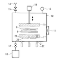
- FIG. 1 shows a sealing process procedure of the method for manufacturing an organic EL panel according to this embodiment.
- FIG. 2 is an example of application to a sealing substrate.
- FIG. 3 is a schematic cross-sectional view of the aligned element substrate and sealing substrate.
- FIG. 4 is a cross-sectional view of the organic EL panel after sealing.
- FIG. 5 is a schematic configuration diagram of the sealing device.
- the organic EL panel sealed and manufactured in the present embodiment has a structure in which a sealing layer is interposed between a device substrate on which an organic EL device is formed and a flat sealing substrate without any gap.
- an organic EL element including an anode 7, an organic light emitting layer 8, and a cathode 9 is formed on a flat glass substrate.
- the anode 7 is a transparent conductive film (ITO) or the like, and is formed by patterning.
- the organic light emitting layer 8 is formed by stacking, for example, a hole injection layer, a hole transport layer, a light emitting layer, an electron transport layer, and an electron injection layer.
- the cathode 9 is an aluminum electrode or the like.
- the organic EL element may be covered with a protective film (not shown).
- the protective film is made of silicon oxide (SiO 2 ), silicon nitride (Si 3 N 4 ), silicon oxynitride (SiON), or the like.
- the organic EL element is deposited from the lower surface of the element substrate as shown in FIG.
- the sealing substrate 1 As the sealing substrate 1, a flat glass substrate is used.
- the sealing substrate 1 is preferably made of homogeneous glass having the same thermal expansion coefficient as the element substrate 6.
- the flatness of the sealing substrate 1 has a warpage of about 0.2 to 0.4 mm as in the liquid crystal display.
- the sealing layer according to this embodiment includes a filler 2, a hygroscopic agent 3, a sealing agent 4, and a fixing agent 5.
- the filler 2 is a curable resin, a non-curable resin, a gel resin, or a high viscosity oil.
- the filler needs to have a coating shape that does not change.
- the viscosity of the filler is preferably high, but the viscosity of the filler 2 is desirably in the range of 10 Pa ⁇ s to 100 Pa ⁇ s in consideration of the coating time and the pressure contact time in the bonding step.
- the hygroscopic agent 3 is highly hygroscopic.
- the hygroscopic agent 3 is assumed to contain 10% or more and 50% or less of a desiccant in a weight ratio in any medium of a curable resin, a non-curable resin, a gel-like resin, or a high viscosity oil. By making it contain in the said range, the moisture-permeable water
- the medium of the hygroscopic agent 3 is not limited, but is preferably made of the same material as the filler 2 because it directly contacts the filler 2. Zeolite or calcium oxide is suitable as the desiccant.
- the desiccant is fine particles sufficiently smaller than the thickness of the sealing layer.
- the particle size of the desiccant is 4 ⁇ m or less, preferably 1 ⁇ m or less.
- the sealant 4 is an ultraviolet curable resin having a low moisture permeability.
- the sealant 4 is preferably an ultraviolet curable epoxy adhesive.
- the sealing agent 4 preferably includes a spacer having a size of 10 ⁇ m or more and 100 ⁇ m or less.
- the spacer is made of glass or plastic, has a spherical or cylindrical shape, has a diameter of 12 ⁇ m, 50 ⁇ m, or the like, and defines the thickness of the sealing layer.
- the fixing agent 5 is an ultraviolet curable resin. It is preferable that the fixing agent 5 has a strong adhesive force and can be cured in a short time.
- the fixing agent 5 is an acrylic adhesive or the like.
- the fixing agent 5 preferably includes a spacer of 10 ⁇ m or more and 100 ⁇ m or less.
- the fixing agent 5 may be the same material as the sealing agent 4.
- the sealing device used in the present embodiment includes an application unit, a sealing unit, an exhaust unit, a gas introduction unit, an alignment unit, a press contact unit, a heating unit, a temporary fixing unit, and a seal curing unit.
- the application means applies the filler 2, the moisture absorbent 3, the sealing agent 4 and the fixing agent 5 to the sealing substrate 1 with a dispenser.
- the sealing means has a structure capable of blocking the bonding chamber 10 from the external environment. In FIG. 5, a gate valve 11 for carrying the substrate in and out of the bonding chamber 10 is provided.
- An exhaust valve 12 and a vacuum pump 13 are connected to the bonding chamber 10 as exhaust means.
- the exhaust means can evacuate the bonding chamber.
- a vent gas 14, a vent valve 15, and a pressure gauge 16 are connected to the bonding chamber 10 as gas introduction means.
- the gas introduction means can control the pressure in the bonding chamber by introducing an inert gas while detecting the internal pressure with the pressure gauge 16.
- the vent gas 14 is an inert gas that is less than a predetermined moisture content.
- the vent gas 14 is nitrogen gas having a moisture concentration of 1 ppm or less.
- the alignment means does not require a high-precision CCD camera alignment like a display, and is a mechanical alignment based on a glass substrate end surface of about ⁇ 100 ⁇ m, and isolates the element substrate 6 and the sealing substrate 1 from each other. Can be aligned by position.
- the pressure welding means is composed of a pair of surface plates (lower surface plate 17 and upper surface plate 18) arranged in the bonding chamber, and can control the load in a vacuum environment.
- the lower surface plate 17 and the upper surface plate 18 are arranged in parallel in order to press-contact the element substrate 6 and the sealing substrate 1.
- the surface plate is preferably made of a conductive metal such as steel.
- the lower surface plate 17 and the upper surface plate 18 have their surfaces flatly contacted with the sealing substrate 1 and the element substrate 6 respectively polished.
- a lifting mechanism 19 is connected to the upper surface plate 18, and the load is controlled by moving the upper surface plate 18 up and down by the lifting mechanism 19.
- the lower surface plate 17 may be a movable surface plate instead of the upper surface plate 18.
- the lower surface plate 17 is provided with a UV transmission hole 20 penetrating the lower surface plate 17.
- the UV transmission hole 20 is appropriately disposed at a position where the fixing agent 5 can be selectively irradiated with ultraviolet rays.
- a UV transmission window 21 is provided on the wall surface of the bonding chamber 10.
- the UV transmission window 21 is arranged at a position where the fixing agent can be irradiated with ultraviolet rays by the spot type ultraviolet lamp 22 from the back surface side of the lower surface plate 17 through the UV transmission hole 20.
- the spot type ultraviolet lamp 22 is disposed outside the bonding chamber.
- the temporary fixing means for the UV transmitting hole 20, the UV transmitting window 21, and the spot type ultraviolet lamp 22 may be provided on the upper surface plate side.
- the heating means is a heater 23, a thermocouple, or the like, and can heat-control the sealing substrate 1 to a desired temperature.
- the planar heater 23 and the thermocouple are disposed in contact with the back surface side of the lower surface plate 17 (the surface opposite to the surface with which the substrate contacts). This heating means indirectly heat-controls the sealing substrate 1 by directly heating the lower surface plate 17 and bringing the sealing substrate 1 into contact with the lower surface plate 17.
- the seal curing means (not shown) is located outside the bonding chamber 10 and cures the sealant by irradiating ultraviolet rays.
- the manufacturing method of the organic EL panel according to the present embodiment includes an application process, a bonding process, and a seal curing process.
- a filler 2, a hygroscopic agent 3, a sealing agent 4, and a fixing agent 5 are sequentially applied to the sealing substrate 1.
- the application is performed in an inert environment where the water content is below a predetermined amount.
- the predetermined amount of moisture is appropriately set according to the standard of the organic EL panel to be manufactured.
- the atmospheric pressure is a nitrogen atmosphere having a moisture concentration of 1 ppm or less.
- a dispenser is used to apply the filler 2, the hygroscopic agent 3, the sealing agent 4 and the fixing agent 5.
- Application of the filler 2 is more productive in screen printing, but it takes time to change the setup because a screen printing plate specialized in panel shape and dimensions is used. descend.
- thermosetting resin as the filler 2
- the productivity is low by itself, the changeover can be changed instantaneously only by selecting a drawing program.
- the sealant 4 and the fixed adhesive 5 after applying the filler screen printing cannot be applied, and application by a dispenser is indispensable.
- productivity is low, it can be compensated by installing multiple facilities. In that case, it is desirable that the same kind of equipment is consistent. In order to improve productivity, it is possible to cope with improvement in coating speed, multiple dispenser nozzles, multiple nozzle heads, multiple dispensers, and the like.
- FIG. 2 shows an example of a four-sided substrate in which four organic EL elements are formed on a substrate and divided to complete four panels.
- the filler 2 is applied at a position facing the organic EL element on the sealing substrate.
- the filler 2 is preferably applied in the form of intermittent straight lines spaced in parallel or in the form of equidistant spirals.
- the filler 2 is preferably applied so that the stretch ratio P / R between the application diameter R of the filler 2 and the application pitch P is in the range of 8 to 32.
- a hygroscopic agent 3 is applied to the outer periphery of the filler 2.
- a sealing agent 4 is applied so as to surround the filler 2 and the hygroscopic agent 3.
- the fixing agent 5 is applied in the form of dots or lines around the sealing substrate 1 or around the sealing agent 4.
- the hygroscopic agent 3 is desirably applied at a position where the stretched width after the pressure contact is within the interval from the inner peripheral edge of the sealing agent 4 to the light emitting outer peripheral edge of the organic EL element.
- the bonding process includes an alignment process, a heating process, a defoaming process, a pressure adjustment process, a pressure welding process, a gas introduction process, and a temporary fixing process.
- the element substrate 6 and the sealing substrate 1 are passed through the gate valve 11 and carried between the lower surface plate 17 and the upper surface plate 18 of the bonding chamber.
- the element substrate 6 and the sealing substrate 1 are arranged so as to face each other so that the surface on which the organic EL element is formed and the surface on which the filler 2 or the like is applied, and are aligned at positions separated from each other by the alignment means.
- the substrates are held in isolation by the holding mechanism, and the respective substrates are aligned by the positioning mechanism.
- the lower surface plate 17 is previously heated to 40 ° C. to 80 ° C., preferably 40 ° C. to 60 ° C., by a heating means. Thereby, when the sealing substrate 1 is brought into contact with the lower surface plate 17, heating can be started immediately.
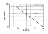
- FIG. 6 shows an example in which the relationship between the viscosity of the coating material of the filler 2, the hygroscopic agent 3, and the sealing agent 4 and the material temperature is measured in the heating of the lower surface plate 17.
- the horizontal axis represents the temperature of the applied material
- the vertical axis represents the viscosity.
- As the coating material an ultraviolet curable epoxy adhesive having a high viscosity was used.
- the viscosity decreased to about 1 ⁇ 2 when the temperature increased by 10 ° C.
- the temperature of the lower surface plate 17 is in the range of 40 ° C. to 80 ° C., desirably in the range of 40 ° C. to 60 ° C.
- the defoaming step is performed for a predetermined time according to the materials of the filler 2, the hygroscopic agent 3, the sealing agent 4, and the fixing agent 5.
- the predetermined time is, for example, about 10 to 60 seconds.
- the exhaust valve 12 is closed, the vent valve 15 is opened, and the vent gas (inert gas) 14 is introduced into the bonding chamber.
- the pressure in the bonding chamber is detected by the pressure gauge 16, and the pressure in the bonding chamber is controlled to 50 Pa to 500 Pa, preferably 50 Pa to 200 Pa.
- the pressure in the bonding chamber is 500 Pa
- the pressure is returned to atmospheric pressure (100 kPa)
- the size of the bubbles contained in the filler 2 or the like is reduced to 5 / 1,000.
- the filler 2, the adsorbent 3, and the sealant 4 are in an uncured state and have a considerable fluidity. Therefore, when the pressure returns to atmospheric pressure, the air is uniformly pressurized at 100 KPa, so that the gap is reduced to a point where it cannot be visually confirmed.
- the vent valve 15 is closed, the upper surface plate 18 is lowered, and the element substrate 6 and the sealing substrate 1 are brought into contact with and pressed against the lower surface plate 17.
- the lower platen 17 is already heated by the heating means 23 and is temperature-controlled by a temperature controller (not shown).
- the sealing substrate 1 is heated by heat conduction by being in contact with the lower surface plate 17, and reduces the viscosity of the filler 2, the hygroscopic agent 3, and the sealing agent 4.
- the pressurizing force required to stretch the filler 2 and the like is reduced, so that the pressure contact time is shortened and the stress on the element is reduced.
- the upper surface plate 18 presses the element substrate 6 and the sealing substrate 1 with a predetermined pressure for a predetermined time, and extends the filler 2, the moisture absorbent 3, and the sealant 4 without a gap.
- pressure welding is performed at a pressure of 5 kPa to 50 kPa for 15 seconds to 60 seconds.
- the thickness of the sealing layer composed of the filler 2, the hygroscopic agent 3, and the sealing agent 4 is 10 ⁇ m to 100 ⁇ m, preferably 20 ⁇ m to 50 ⁇ m.
- the fixing agent 5 is cured by irradiating the spot type ultraviolet lamp 22 with ultraviolet rays.
- a radiation energy of 3 W / cm 2 can be obtained with a wavelength of 365 nm and a diameter of 5 mm, and even an ultraviolet curable epoxy adhesive can be cured at 6 J.
- the fixing agent 5 is cured.
- the temporarily fixed substrate passes through the gate valve 11 and is carried out of the bonding chamber 10 and further in a normal environment such as a clean room.
- a temporarily fixed substrate is set in a simple UV cut mask folder, and is put into a general-purpose ultraviolet irradiation conveyor to cure the sealant 4.
- the sealing agent 4 may be cured by moving the spot type ultraviolet lamp 22 while irradiating the sealing agent 4.
- the sealing agent 4 is not completely cured, but the organic EL element is covered with the filler 2 and the moisture absorbing agent 3 and sealed. Therefore, even if the temporarily fixed substrate is in a general environment with moisture and particles, the organic EL element is not affected at all.
- the sealing is completed by placing the substrate on which the sealing agent 4 has been cured into an oven and after-curing.
- a thermosetting resin is used for the filler 2 and the hygroscopic agent 3, it is cured by being put in an oven.
- the organic EL panel is completed by dividing the last bonded substrate.
- the heating means 23 it is possible to reduce the viscosity of the filler 2, the hygroscopic agent 3, and the sealing agent 4 and reduce the impossibility of applying a load to the organic EL element during pressure contact. Thereby, element damage is reduced and yield is improved. Moreover, there is no air bubble inside the seal, and a high quality panel can be manufactured.
- the sealing agent is cured immediately after the pressure-welding step, it is necessary to use at least one surface plate as a quartz surface plate having ultraviolet transparency.
- Quartz surface plate is (1) expensive, (2) difficult to flatly polish, (3) low in strength compared to steel, etc., so it is easily deformed during pressure welding and evacuation, and the sealing layer is processed uniformly.
- the inside of the bonding chamber is a dry environment with a low water content, when a glass substrate is pressed with quartz, peeling electrification, which is very large static electricity, occurs at the time of dissociation, and the pressed substrate becomes There were problems such as strong sticking to the surface plate and major problems.
- the pair of surface plates can be made of metal by separating the seal hardening step from the temporary fixing step.
- the upper and lower surface plates made of metal such as steel, a surface plate having high flatness and a small thickness can be manufactured at low cost.
- the sealing thickness can be made uniform, and a high-quality organic EL panel can be manufactured.
- the metal surface plate has an advantage that the generation of static electricity is very small because it has conductivity. As a result, the generation of static electricity is drastically reduced, and defects caused by static electricity are reduced.
- a metal hydride lamp which is an ultraviolet light source
- the metal hydride lamp generates a large amount of heat and needs to be separated from the substrate so as not to have a thermal effect on the organic EL element.
- the UV light illuminance per unit area decreases. Since the curing energy of the ultraviolet curable epoxy resin is as high as 6,000 mJ or more, the most time-consuming process in the conventional solid sealing process is an ultraviolet curing process for curing the sealant.
- the bonding step only the fixing agent is cured in a short time after pressure contact, and the element substrate and the sealing substrate are temporarily fixed, so that the substrate is kept in a general environment in a state where the sealing agent is uncured. It was possible to carry it out.
- the processing time of the bonding process can be shortened.
- a time-consuming sealant curing step can be cured using a general-purpose UV curing device or heating device in a general environment. Thereby, batch processing with an inexpensive facility is also possible.
- metal halide lamps generate a large amount of heat and generate ozone, when they are used in a clean room, a large amount of cooling air and ozone discharge from outside air separated from the clean room is required, resulting in a large facility.
- the vacuum container can be reduced in size, and the entire surface of the substrate is not irradiated with ultraviolet rays, so that the substrate temperature does not increase.
- the spot type ultraviolet lamp can use glass fiber light guide irradiation, but the LED type ultraviolet lamp can be used, and there is no generation of ozone due to unnecessary short wavelength like a metal halide lamp, so the equipment is made compact. There is also an effect that can be done.
- an ultraviolet curing mask was required for each shape of the organic EL element.
- the seal curing process is separated from the temporary fixing process, it is not necessary to use an ultraviolet curing mask in a dry or vacuum environment, so that no setup change in a dry or vacuum environment is required. . Thereby, the time for evacuation and vent gas introduction can be shortened, and productivity is improved.
- FIG. 7 shows a cross section of the coating dimensions, taking the filler as an example.
- FIG. 7A is an assumed cross-sectional view immediately after the filler 2 having the diameter R corresponding to the nozzle diameter is applied to the substrate 1 at the pitch P by the dispenser.
- FIG. 7B is an assumed cross-sectional view when the filler 2 spreads from the relationship between the viscosity and the substrate surface wettability after application. Experimentally, it was confirmed that the filler 2 applied with the diameter R spreads 4 times, and the spread width after application becomes 4R.
- FIG. 7 (c) is an assumed cross-sectional view that is spread evenly without gaps and stretched to the sealing layer thickness d by pressure welding.
- the pitch P is wide with a large coating diameter R from the viewpoint of productivity.
- a large load is required, and a long time is required for the pressure contact time, and a large stress is applied to the element. Since the pressure contact time and the element stress are contradictory characteristics, the balance is important.
- FIG. 8 shows the relationship between coating conditions and coating time.
- the horizontal axis represents the pitch P
- the vertical axis (left) represents the coating diameter R
- the vertical axis (right) represents the coating time.
- the figure shows the result of calculating the application time under the conditions that the application area of the filler is 140 mm ⁇ 140 mm, the application speed is 50 mm / s, and the sealing thickness d is 12, 25, and 50 ⁇ m. It was found that the coating time decreased sharply in the fine pitch P region and gradually changed in the wide pitch region.
- FIG. 9 shows the relationship between coating conditions and spread.
- the horizontal axis represents the pitch P
- the vertical axis represents the stretch ratio (P / R).
- the application conditions were the same as in FIG.
- the actual pressure welding is an operation of expanding the spread width 4R after coating to the pitch P
- the P / 4R ratio is optimally 2 or more and 8 or less, preferably 3 or more and 6 or less. If it is less than this, the application time becomes longer, and if it is more than this, the pressure contact load becomes larger. Accordingly, the optimum range of the draw ratio (P / R) is 8 or more and 32 or less, preferably 12 or more and 24 or less.
- the sealing thickness is 25 ⁇ m
- the stretch ratio P / R is in the range of 12 to 24
- the pitch P is optimally in the range of 4.5 mm to 18 mm, and this pitch range is obtained from FIG. It can be seen that the coating diameter R is optimally 0.4 mm to 0.8 mm.
- FIG. 10 is a schematic cross-sectional view of an organic EL panel after sealing according to this modification.
- the filler used in this modification the hygroscopic agent 3 is used.
- the filler is assumed to contain 10% or more and 50% or less of a desiccant in a weight ratio in a medium of curable resin, non-curable resin, gel resin, or high viscosity oil.
- the filler is preferably made of the same material as the hygroscopic agent. Zeolite or calcium oxide is suitable as the desiccant.
- the desiccant is fine particles sufficiently smaller than the thickness of the sealing layer.
- the particle size of the desiccant is 4 ⁇ m or less, preferably 1 ⁇ m or less.
- the viscosity of the filler is desirably in the range of 10 Pa ⁇ s to 100 Pa ⁇ s.
- the filler is applied at a position facing the organic EL element on the sealing substrate.
- the sealing thickness is 10 ⁇ m to 100 ⁇ m.
- the desiccant contained in the filler is a fine particle that is sufficiently small with respect to this sealing thickness, so leakage current is generated due to deformation of the sealing thickness during pressure contact of the seal and local concentrated load after completion of the panel. It does not cause a defect such as a short circuit.
- FIG. 11 is a schematic cross-sectional view of the sealing device according to this embodiment.
- the bonding chamber 24 is not a vacuum chamber but a sealed chamber similar to a glove box.
- a gas circulation purifier (not shown) is connected to the bonding chamber 24 so that the inside of the bonding chamber can be a dry environment with little moisture.
- the bonding chamber 24 has no gate valve and is connected to the transfer chamber in an open state.
- the bonding chamber 24 includes an inner chamber 25 as a sealing means.
- the inner chamber 25 is connected to the lifting mechanism 19 of the upper surface plate 18 so as to accommodate the upper surface plate 18, the element substrate 6, and the sealing substrate 1.
- the inner chamber 25 is lowered as the upper surface plate 18 moves up and down, and comes into contact with the lower surface plate 17.
- a vacuum seal 26 is disposed at a portion of the lower surface plate 17 that contacts the inner chamber 25, and a sealed space can be formed by the inner chamber 25 and the lower surface plate 17. That is, the inner chamber 25 can block the space where the bonding is actually performed from the external environment.
- An exhaust valve 12 and a vacuum pump 13 are connected to the inner chamber 25 as exhaust means.
- the exhaust means can evacuate the bonding chamber.
- the inner chamber 25 is connected to a vent gas 14, a vent valve 15, and a pressure gauge 16 as gas introduction means.
- the gas introduction means can control the pressure in the inner chamber by introducing an inert gas while detecting the internal pressure with the pressure gauge 16.
- the vent gas 14 is an inert gas that is less than a predetermined moisture content.
- the vent gas is nitrogen gas having a moisture concentration of 1 ppm or less.
- the lower surface plate 17 is provided with a UV transmission hole 20 penetrating the lower surface plate 17.
- the UV transmission hole 20 is appropriately disposed at a position where the fixing agent 5 can be selectively irradiated with ultraviolet rays.
- a UV transmission window 21 is provided at the end of the UV transmission hole 20 on the lower surface of the lower surface plate.
- the spot type ultraviolet lamp 22 is in the bonding chamber and is arranged at a position where the fixing agent 5 can be irradiated with ultraviolet rays through the UV transmission window 21 from the back surface side of the lower surface plate 17.
- the temporary fixing means for the UV transmitting hole 20, the UV transmitting window 21, and the spot type ultraviolet lamp 22 may be provided on the upper surface plate side.
- the lower surface plate 17 is the bottom surface of the inner chamber 25, but a lower inner chamber may be provided separately.
- the lower inner chamber is configured to accommodate the lower surface plate 17.
- the UV transmission window 21 is preferably provided in the lower inner chamber at a position where the fixing agent can be irradiated with ultraviolet rays through the UV transmission hole 20.
- An elastic sheet 27 is provided on the surface of the upper surface plate 18 on the element substrate side.
- the thickness of the elastic sheet 27 is preferably 0.1 mm to 1 mm.
- the elastic sheet 27 is made of a slightly conductive material for static electricity countermeasures.
- the material has a surface resistance of 10 10 ⁇ / ⁇ or less or a volume resistivity of 10 12 ⁇ ⁇ m or less.
- the resistance of the front and back surfaces should be 10 10 ⁇ or less. It ’s fine.
- a 0.5 mm thick antistatic polyethylene porous film (Sunmap manufactured by Nitto Denko Corporation) was used.
- the surface plate is flattened by polishing, but the flatness is about 5 ⁇ m. Furthermore, the flatness of the platen for large substrates is further reduced. When the sealing thickness is reduced even for a small substrate, the flatness of the surface plate affects the variation in the sealing thickness.
- an error in the flatness of the upper and lower surface plates can be absorbed by arranging a slightly conductive elastic sheet 27 for static electricity on the upper surface plate. Specifically, by setting the thickness of the elastic sheet 27 within the above range, flatness of several to several tens of ⁇ m can be absorbed. Thereby, the sealing thickness can be made uniform.
- glass is generally used for the element substrate 6, but when the elastic sheet 27 is insulative, electrostatic peeling charge is generated at the time of peeling, and the bonded substrate is electrostatically attracted to the upper surface plate. And will not leave.
- the element substrate 6 on which the organic EL element is formed and the sealing substrate 1 on which the filler 2, the hygroscopic agent 3, the sealing agent 4 and the fixing agent 5 are applied are carried in from the substrate carry-in / out port 28.
- the inner chamber 25 and the upper surface plate 18 are lowered, and only the inner chamber 25 is in contact with the lower surface plate 18 at a position where the upper surface plate 18 does not contact the element substrate 6 and is sealed by the vacuum seal 26.
- evacuation and pressure adjustment are performed in the same manner as in the first embodiment, and the upper platen 18 is lowered by the lifting mechanism 19 to press-contact the element substrate 6 and the sealing substrate 1.
- the fixing agent 5 is UV cured by the spot type ultraviolet lamp 22.
- the upper substrate 18 and the inner chamber 25 are raised, and the bonded substrates are unloaded from the substrate loading / unloading port 27.
- the elevating mechanism 19 and the spot type ultraviolet lamp 22 can be installed in the bonding chamber.
- the volume to be evacuated can be limited to the volume necessary for bonding. Thereby, the time required for evacuation and venting can be shortened, so that productivity is improved.
- the elastic sheet 27 by providing the elastic sheet 27, a uniform sealing thickness can be ensured even when the sealing thickness is reduced or the substrate has a large area. . Thereby, the quality and yield of the organic EL panel are improved.
- FIG. 12 shows a schematic cross-sectional view of the sealing device. In the figure, the description of the bonding chamber, the sealing means, the vacuum exhaust means, and the gas introducing means is omitted.
- the vacuum suction device includes a vacuum suction hole 29, a suction valve 30, a vacuum suction pump 31, a suction release valve 32, and a release gas 33.
- the vacuum suction holes 29 are provided in the lower surface plate 17 and have a plurality of openings that open toward the sealing substrate side surface of the lower surface plate 17. Each of the plurality of openings is connected to a vacuum suction pump 31 via a suction valve 30. The plurality of openings are also connected to a release gas 33 via adsorption release valves 32, respectively.
- the release gas 33 is nitrogen gas having a moisture concentration of 1 ppm or less. Further, the porous elastic sheet described in the second embodiment may be used in combination on the suction surface, and vacuum suction becomes easier.
- the suction valve 30 is opened, and the sealing substrate 1 is absorbed onto the lower surface plate 17 by the vacuum suction pump 31. Thereafter, the element substrate 6 is carried into the bonding chamber and aligned. And the process after a defoaming process is implemented similarly to 2nd Embodiment. That is, the suction valve 30 is closed, defoaming is performed by evacuation, the pressure is adjusted, and the substrate is pressed. Next, at the same time as returning the substrate to atmospheric pressure in the gas introduction step, the release valve 32 is opened, the release gas 33 is introduced to atmospheric pressure, and the sealing substrate 1 is opened. Thereafter, the upper surface plate 18 is raised and the bonded substrates are carried out.
- the sealing substrate 1 is in close contact with the lower surface plate 17.
- the heat conduction efficiency to the sealing substrate 1 is improved, the filler 2 and the like can be sufficiently soaked in a short time.
- the productivity of the organic EL panel is improved.
- the viscosity of the filler or the like can be sufficiently lowered before the press-contacting process, stress on the element can be reduced, and quality and yield can be improved.
- the present embodiment is characterized in that a gas pressurizing mechanism and a gas pressure adjusting mechanism are added to the configuration of the sealing device of the first embodiment.
- the sealing device according to the present embodiment includes a vacuum suction mechanism as in the third embodiment.
- the configuration not particularly described is the same as that of the first embodiment.
- FIG. 13 is a schematic cross-sectional view of the sealing device according to this embodiment. In the figure, the description of the bonding chamber, the sealing means, the vacuum exhaust means, and the gas introducing means is omitted.
- the gas pressurizing mechanism is composed of an upper platen hole 34, an ejection valve 35, and a pressurized gas 36.
- the upper surface plate hole 34 is provided in the upper surface plate 18, and has a plurality of openings that open toward the element substrate side surface of the upper surface plate 18. Each of the plurality of openings is connected to the pressurized gas 36 via the ejection valve 35.
- a pressure controller 37 is provided as a gas pressure adjusting mechanism between the ejection valve 35 and the pressurized gas 36.
- the pressurized gas 36 is nitrogen gas having a moisture concentration of 1 ppm or less.
- the plurality of openings may be connected to the vacuum suction pump 31 via the suction valves 38, respectively.
- the vacuum suction pump may be common with the vacuum suction mechanism of the lower surface plate.
- the suction valve 30 is opened, and the sealing substrate 1 is adsorbed to the lower platen 17 by the vacuum suction pump 31.
- the element substrate is carried into the 6 bonding chamber, aligned, and held.
- the vacuum suction valve 30 is closed, defoaming is performed, the pressure is adjusted, and the upper surface plate 18 is lowered to press the substrate.
- the substrate is returned to atmospheric pressure in the gas introduction process.
- the 35 ejection valve is opened while maintaining the pressure contact state, and the pressurized gas 36 adjusted to a predetermined pressure by the pressure regulator is ejected from the upper plate hole 34. Thereby, a gas layer is generated between the upper surface plate 18 and the element substrate 6.
- the upper surface plate 18 presses the substrate with a load of 10 kPa
- a gas having a pressure 10 kPa higher than the pressure in the bonding chamber is introduced by the gas pressurizing mechanism, the upper surface plate 18 slightly floats, Gas leaks from the gap on the outer periphery of the substrate 6.
- the gap between the element substrate 6 and the upper surface plate 18 that floats is filled with pressurized gas, and the surface of the element substrate 6 is pressurized with a uniform pressure with a load close to the load of the upper surface plate 18. become.
- the pressurization point of the upper surface plate 18 is the center of the surface plate, but according to the present embodiment, the pressurization point can be around the upper surface plate.
- the pressure point of the surface plate is around the surface plate. Furthermore, by using the porous elastic sheet described in the second embodiment in combination, the hermeticity of the pressurized gas is improved and the effect of uniform pressurization is enhanced.
- the fixing agent 5 is irradiated with ultraviolet rays to temporarily fix the pressed substrate. Thereafter, the ejection valve 35 is closed, the upper surface plate 18 is raised, and the bonded substrates are carried out.
- the upper surface plate hole 34 is the same as the vacuum suction mechanism.
- the vacuum suction valve 38 By connecting the vacuum suction valve 38 to the vacuum suction pump 31, the upper surface plate 18 is vacuum-sucked when the element substrate 6 is loaded. You can also. Thereby, when the element substrate 6 is carried in, it can be vacuum-adsorbed to the upper surface plate 18. However, the vacuum adsorption function is up to the defoaming step for evacuating the bonding chamber.
- a mechanism similar to the vacuum suction mechanism is provided on the surface plate on the element side, and the pressure-adjusted gas is ejected from the surface plate, whereby the element substrate is evenly distributed per unit area according to the Pascal principle.
- a load can be applied.
Landscapes
- Engineering & Computer Science (AREA)
- Manufacturing & Machinery (AREA)
- Physics & Mathematics (AREA)
- Optics & Photonics (AREA)
- Electroluminescent Light Sources (AREA)
Abstract
Description
しかしながら、中空封止を大型の有機EL素子に適用した場合には、中空部分において封止基板が有機EL素子と接触し、有機EL素子が損傷する問題がある。 In a conventional sealing process, a sealing substrate such as a metal cap or sealing glass provided with a space inside is used and sealed with a sealing portion. In the internal space, a desiccant or a dry sheet that adsorbs moisture is incorporated to absorb permeated moisture from the peripheral seal portion. This sealing method is also called hollow sealing, and is applied to a small organic EL element.
However, when hollow sealing is applied to a large-sized organic EL element, there is a problem that the sealing substrate comes into contact with the organic EL element in the hollow portion and the organic EL element is damaged.
また、特許文献1には明示されていないが、一般にシール剤の硬化は、全面紫外線照射によって行われるが、該方法では、圧接及び硬化を1工程として連続処理しなければならず、時間がかかり、タクトタイムが長くなる。また、単純な圧接では素子基板と封止基板との平行度が保てず、素子の損傷の要因となる。また、パネルサイズの異なる基板を封止する場合、紫外線硬化時の紫外線カットマスクの交換が必要となり、段取り替に時間がかかり、生産性を低下させる。更に、圧接時の荷重(加圧力)が大きいと、素子損傷の要因となる。 In
Although not explicitly disclosed in
図1は、本実施形態に係る有機ELパネルの製造方法の封止処理手順である。図2は、封止基板への塗布例である。図3は、位置合わせした素子基板及び封止基板の概略断面図である。図4は、封止後の有機ELパネルの断面図である。図5は、封止装置の概略構成図である。 [First Embodiment]
FIG. 1 shows a sealing process procedure of the method for manufacturing an organic EL panel according to this embodiment. FIG. 2 is an example of application to a sealing substrate. FIG. 3 is a schematic cross-sectional view of the aligned element substrate and sealing substrate. FIG. 4 is a cross-sectional view of the organic EL panel after sealing. FIG. 5 is a schematic configuration diagram of the sealing device.
有機EL素子は、保護膜(不図示)で被覆されていても良い。保護膜は、酸化珪素(SiO2)、窒化珪素(Si3N4)、酸窒化珪素(SiON)等とされる。
本実施形態では、蒸着成膜のため、図3のように有機EL素子は素子基板の下面より蒸着されている。 In the
The organic EL element may be covered with a protective film (not shown). The protective film is made of silicon oxide (SiO 2 ), silicon nitride (Si 3 N 4 ), silicon oxynitride (SiON), or the like.
In this embodiment, the organic EL element is deposited from the lower surface of the element substrate as shown in FIG.
本実施形態に係る封止層は、充填剤2、吸湿剤3、及びシール剤4、固定剤5から構成されている。 As the sealing
The sealing layer according to this embodiment includes a
密閉手段は、貼り合せ室10を外部環境から遮断可能な構造とされる。図5では、貼り合せ室10に基板を搬出入するための仕切弁11が設けられている。 The application means (not shown) applies the
The sealing means has a structure capable of blocking the
位置合わせ手段は、ディスプレイのような高精度のCCDカメラ・アライメントは必要なく、±100μm程度のガラス基板端面を基準とする機械的アライメントなどとされ、素子基板6と封止基板1とを隔離した位置で位置合わせすることができる。 An
The alignment means does not require a high-precision CCD camera alignment like a display, and is a mechanical alignment based on a glass substrate end surface of about ± 100 μm, and isolates the
封止基板1に、充填剤2、吸湿剤3、シール剤4、及び固定剤5を順に塗布する。塗布は、水分が所定量を下回る不活性環境下で実施する。水分の所定量は、製造する有機ELパネルの規格に応じて適宜設定される。例えば、不活性環境下とは、水分濃度が1ppm以下の大気圧の窒素雰囲気とされる。 (Coating process)
A
まず、図2(a)に示すように、充填剤2を封止基板上の有機EL素子に相対する位置に塗布する。充填剤2は、平行に間隔を隔てた断続直線状、または、等間隔螺旋状に塗布すると良い。充填剤2は、充填剤2の塗布径の直径Rと、塗布ピッチPとの延伸比P/Rが8以上32以下の範囲内になるように塗布すると良い。
次に、図2(b)に示すように、充填剤2の外周に吸湿剤3を塗布する。さらに、図2(c)に示すように、充填剤2及び吸湿剤3を囲うようにシール剤4を塗布する。その後、封止基板1の周辺またはシール剤4の周辺に、固定剤5を点状または線状に塗布する。 FIG. 2 shows an example of a four-sided substrate in which four organic EL elements are formed on a substrate and divided to complete four panels.
First, as shown in FIG. 2A, the
Next, as shown in FIG. 2B, a
貼り合せ工程は、位置合わせ工程、加熱工程、脱泡工程、圧力調整工程、圧接工程、ガス導入工程、及び仮固定工程を備えている。 (Lamination process)
The bonding process includes an alignment process, a heating process, a defoaming process, a pressure adjustment process, a pressure welding process, a gas introduction process, and a temporary fixing process.
素子基板6及び封止基板1を、仕切り弁11を通過させ、貼り合せ室の下定盤17と上定盤18との間に搬入する。素子基板6及び封止基板1は、有機EL素子が形成された面と充填剤2などが塗布された面とが向かい合うよう対向配置され、位置合わせ手段により互いに隔離した位置で位置合わせする。図示されていないが、保持機構により隔離して保持され、位置決め機構によりそれぞれの基板が位置合わせされる。 (Positioning process)
The
予め加熱手段により下定盤17を40℃~80℃、好ましくは40℃~60℃に加熱しておく。それにより、下定盤17に封止基板1を接触させた際に、直ちに加熱を開始することが可能となる。
ここで、加熱の温度範囲の設定根拠を説明する。下定盤17の加熱において、充填剤2、吸湿剤3、及びシール剤4の塗布材料の粘度と材料温度の関係を測定した一例を図6に示す。同図において、横軸が塗布した材料の温度、縦軸が粘度である。塗布材料としては、高めの粘度を有する紫外線硬化型エポキシ系接着剤を使用した。図6によれば、温度が10℃上昇すると粘度が約1/2に減少した。室温の25℃で100Pa・sの塗布材料を60℃に昇温すると10Pa・sとなり粘度が1/10に低下し、流動性が著しく向上した。よって、下定盤17の温度は、40℃~80℃の範囲、望ましくは40~60℃の範囲が好適である。 (Heating process)
The
Here, the basis for setting the temperature range of heating will be described. FIG. 6 shows an example in which the relationship between the viscosity of the coating material of the
素子基板6及び封止基板1を位置合わせした後、仕切り弁11を閉じ、排気バルブ12を開放し、真空ポンプ13により、貼り合せ室内を10Pa以上50Pa以下の範囲となるよう真空排気する。貼り合せ室内を真空とすることで、充填剤2、吸湿剤3、シール剤4、及び固定剤5に内包される気体を除くことができる。但し、この圧力領域では、充填剤2、吸湿剤3、シール剤4に含まれている添加物や低分子量成分が蒸発し続け、発泡し続けるため、材料性能と形状保持の点から好ましくない。よって、脱泡工程は、充填剤2、吸湿剤3、シール剤4、及び固定剤5の材質に応じて、所定時間実施される。所定時間は、例えば、10秒~60秒程度とされる。 (Defoaming process)
After the
脱泡工程の後、排気バルブ12を閉じ、ベントバルブ15を開放して、貼り合せ室内にベントガス(不活性ガス)14を導入する。この際、貼り合せ室内の圧力を圧力計16により検出し、貼り合せ室内の圧力を50Pa以上500Pa以下、好ましくは50Pa以上200Pa以下に制御する。貼り合せ室内の圧力を500Paとした場合、大気圧(100kPa)に戻されると、充填剤2などに内包された気泡の大きさは5/1,000の大きさに縮小する。また、圧接時に封止内部に多少の空隙が発生しても、充填剤2、吸着剤3、シール剤4は未硬化状態であり、少なからず流動性を持っている。従って、大気圧に戻ると、100KPaで均等加圧されるため、空隙は目視では確認できないまでに縮小する。 (Pressure adjustment process)
After the defoaming step, the
圧力調整工程の後、ベントバルブ15を閉じ、上定盤18を下降させて、下定盤17との間で、素子基板6と封止基板1とを接触させて圧接する。この際、下定盤17は加熱手段23により既に加熱され、図示されていない温度調節計により温度制御されている。封止基板1は下定盤17に接することによって熱伝導により加熱され、充填剤2、吸湿剤3、及びシール剤4の粘度を低下させる。それにより、充填剤2などを延伸させるために要する加圧力が低下するため、圧接時間が短縮するとともに、素子へのストレスが低減する。
上定盤18は、素子基板6及び封止基板1を所定加圧で所定時間圧接し、充填剤2、吸湿剤3、及びシール剤4と隙間無く延伸させる。例えば、5kPa~50kPaの圧力で、15秒~60秒間圧接する。ここで、充填剤2、吸湿剤3、及びシール剤4からなる封止層の厚さは10μm~100μm好ましくは20μm~50μmとされる。 (Pressing process)
After the pressure adjustment step, the
The
圧接工程の後、ベントバルブ15を開放し、ベントガス14を導入して貼り合せ室内の内部を大気圧に戻す。 (Gas introduction process)
After the pressure welding process, the
ガス導入工程の後、スポット型紫外線ランプ22にて紫外線を照射し、固定剤5を硬化させる。例えば、スポット型紫外線ランプ22としてLED UV照射装置を用いると、波長365nm、直径5mmで、3W/cm2の照射エネルギーを得られ、紫外線硬化型エポキシ接着剤でも6Jで硬化することから、数秒で固定剤5は硬化する。 (Temporary fixing process)
After the gas introduction step, the fixing
仮固定工程の後、仮固定された基板は、仕切り弁11を通過して貼り合せ室10の外、更にクリーンルーム等の通常環境下に搬出される。必要により簡易的なUVカットマスクフォルダに仮固定された基板をセットし、汎用紫外線照射コンベアに投入してシール剤4を硬化させる。なお、シール剤4の硬化は、スポット型紫外線ランプ22をシール剤4に照射しながら移動させて実施しても良い。固定剤5により仮固定された基板において、シール剤4は完全に硬化していないが、有機EL素子は充填剤2及び吸湿剤3で被覆され、密封されている。そのため、仮固定された基板を水分及びパーティクルのある一般環境下であっても、有機EL素子に全く影響のない状態となる。 (Seal curing process)
After the temporary fixing step, the temporarily fixed substrate passes through the
最後に貼り合せた基板を分割することにより、有機ELパネルが完成する。 The sealing is completed by placing the substrate on which the
The organic EL panel is completed by dividing the last bonded substrate.
本実施形態では、貼り合せ工程において、圧接後に固定剤のみを短時間で硬化させて、素子基板と封止基板とを仮固定することで、シール剤が未硬化の状態で基板を一般環境下へと搬出することを可能とした。貼り合せ工程の処理時間を短縮することができる。また、時間を要するシール剤硬化工程を一般環境下で汎用のUV硬化装置または加熱装置を用いて硬化できるようになる。それにより、安価な設備でのバッチ処理も可能となる。 Conventionally, a metal hydride lamp, which is an ultraviolet light source, is used as a means for curing the sealant. The metal hydride lamp generates a large amount of heat and needs to be separated from the substrate so as not to have a thermal effect on the organic EL element. Further, in order to uniformly irradiate ultraviolet rays over a wide range, it is necessary to increase the distance between the sealing substrate and the ultraviolet light source. However, when the distance between the sealing substrate and the ultraviolet light source is increased, the UV light illuminance per unit area decreases. Since the curing energy of the ultraviolet curable epoxy resin is as high as 6,000 mJ or more, the most time-consuming process in the conventional solid sealing process is an ultraviolet curing process for curing the sealant.
In the present embodiment, in the bonding step, only the fixing agent is cured in a short time after pressure contact, and the element substrate and the sealing substrate are temporarily fixed, so that the substrate is kept in a general environment in a state where the sealing agent is uncured. It was possible to carry it out. The processing time of the bonding process can be shortened. In addition, a time-consuming sealant curing step can be cured using a general-purpose UV curing device or heating device in a general environment. Thereby, batch processing with an inexpensive facility is also possible.
図7に、充填剤を例として、塗布寸法の断面を示す。図7(a)は、ディスペンサーにより、基板1上にノズル直径に相当する直径Rの充填剤2をピッチPで塗布した直後の想定断面図である。図7(b)は、充填剤2が塗布後に粘度と基板表面濡れ性との関係から広がった場合の想定断面図である。実験的に直径Rで塗布した充填剤2が4倍に広がり、塗布後の広がり幅4Rになることを確認した。図7(c)は、圧接により空隙もなく均等に広がって封止層厚さdに延伸した想定断面図である。
特に、塗布量の多い充填剤2の塗布は、生産性の観点から、大きい塗布直径RでピッチPを広い方が良い。しかしながら、幅広く延伸するために、大きな荷重が必要となり、更に圧接時間に長時間を要することになり、大きなストレスが素子に掛かることになる。圧接時間と素子ストレスは相反する特性であるため、そのバランスが重要となる。 The basis for setting the coating diameter and coating pitch of the coating material will be described.
FIG. 7 shows a cross section of the coating dimensions, taking the filler as an example. FIG. 7A is an assumed cross-sectional view immediately after the
In particular, when the
本変形例に係る有機ELパネルの製造方法は、充填剤として吸湿剤を用いたことを特徴とする。特に説明がない構成に関しては、第1実施形態と同様とする。図10に、本変形例に係る封止後の有機ELパネルの概略断面図を示す。
本変形例において用いる充填剤は、吸湿剤3を用いる。充填剤は、硬化性樹脂、非硬化性樹脂、ゲル状樹脂、または高粘度オイルのいずれかの媒体に、重量比で10%以上50%以下の乾燥剤が含有されたものとされる。充填剤は吸湿剤と同一の材質が望ましい。乾燥剤としては、ゼオライトまたは酸化カルシウムが適している。乾燥剤は、封止層の厚さより十分に小さい微粒子とされる。乾燥剤の粒径は4μm以下、好ましくは1μm以下とされると良い。充填剤の粘度は、10Pa・s~100Pa・sの範囲が望ましい。 [Modification of First Embodiment]
The manufacturing method of the organic EL panel according to this modification is characterized by using a hygroscopic agent as a filler. The configuration not particularly described is the same as that of the first embodiment. FIG. 10 is a schematic cross-sectional view of an organic EL panel after sealing according to this modification.
As the filler used in this modification, the
本実施形態は、第1実施形態の封止装置の構成に、インナーチャンバー及び弾性シートが追加されたことを特徴とする。特に説明がない構成に関しては、第1実施形態と同様とする。図11に、本実施形態に係る封止装置の概略断面図を示す。 [Second Embodiment]
The present embodiment is characterized in that an inner chamber and an elastic sheet are added to the configuration of the sealing device of the first embodiment. The configuration not particularly described is the same as that of the first embodiment. FIG. 11 is a schematic cross-sectional view of the sealing device according to this embodiment.
本実施形態は、第2実施形態の封止装置の構成に、真空吸着機構が追加されたことを特徴とする。特に説明がない構成に関しては、第2実施形態と同様とする。図12に、封止装置の概略断面図を示す。同図において、貼り合せ室、密閉手段、真空排気手段、及びガス導入手段の記載は省略した。 [Third Embodiment]
The present embodiment is characterized in that a vacuum suction mechanism is added to the configuration of the sealing device of the second embodiment. The configuration not particularly described is the same as that of the second embodiment. FIG. 12 shows a schematic cross-sectional view of the sealing device. In the figure, the description of the bonding chamber, the sealing means, the vacuum exhaust means, and the gas introducing means is omitted.
真空吸着孔29は、下定盤17に設けられており、下定盤17の封止基板側の面に向けて開口する複数の開口部を有する。複数の開口部はそれぞれ吸着バルブ30を介して真空吸着ポンプ31に接続されている。また、複数の開口部は、それぞれ吸着リリースバルブ32を介してリリースガス33にも接続されている。リリースガス33は、水分濃度1ppm以下の窒素ガスなどとされる。
また、吸着面に第2実施形態で説明した多孔質の弾性シートを併用しても良く、より真空吸着が容易となる。 The vacuum suction device includes a
The vacuum suction holes 29 are provided in the
Further, the porous elastic sheet described in the second embodiment may be used in combination on the suction surface, and vacuum suction becomes easier.
本実施形態は、第1実施形態の封止装置の構成に、ガス加圧機構及びガス圧力調整機構が追加されたことを特徴とする。また、本実施形態に係る封止装置は、第3実施形態と同様に真空吸着機構を備えている。特に説明がない構成に関しては、第1実施形態と同様とする。図13に、本実施形態に係る封止装置の概略断面図を示す。同図において、貼り合せ室、密閉手段、真空排気手段、及びガス導入手段の記載は省略した。 [Fourth Embodiment]
The present embodiment is characterized in that a gas pressurizing mechanism and a gas pressure adjusting mechanism are added to the configuration of the sealing device of the first embodiment. Moreover, the sealing device according to the present embodiment includes a vacuum suction mechanism as in the third embodiment. The configuration not particularly described is the same as that of the first embodiment. FIG. 13 is a schematic cross-sectional view of the sealing device according to this embodiment. In the figure, the description of the bonding chamber, the sealing means, the vacuum exhaust means, and the gas introducing means is omitted.
更に、第2実施形態で説明した多孔質弾性シートを併用することにより、加圧ガスの密閉性が向上し、より均一加圧の効果が高まる。 For example, when the
Furthermore, by using the porous elastic sheet described in the second embodiment in combination, the hermeticity of the pressurized gas is improved and the effect of uniform pressurization is enhanced.
2 充填剤
3 吸湿剤
4 シール剤
5 固定剤
6 素子基板
7 陽極
8 有機発光層
9 陰極
10,24 貼り合せ室
11 仕切り弁
12 排気バルブ
13 真空ポンプ
14 ベントガス
15 ベントバルブ
16 圧力計
17 下定盤
18 上定盤
19 昇降機構
20 UV透過孔
21 UV透過窓
22 スポット型紫外線照射ランプ
23 面状ヒータ
25 インナーチャンバー
26 真空シール
27 弾性シート
28 基板搬出入口
29 真空吸着孔
30,38 吸着バルブ
31 真空吸着ポンプ
32 吸着リリースバルブ
33 リリースガス
34 上定盤孔
35 噴出バルブ
36 加圧ガス
37 圧力制御器 DESCRIPTION OF
Claims (16)
- 有機EL素子が形成された素子基板と、平坦な封止基板との間に、封止層を隙間無く介在させた有機ELパネルの製造方法において、
水分が所定量を下回る不活性環境下で、前記有機EL素子の位置に相対する前記封止基板の位置に、充填剤、吸湿剤、前記充填剤及び吸湿剤を囲うように配置される紫外線硬化型樹脂であるシール剤、及び紫外線硬化型樹脂である固定剤を、それぞれ独立に塗布する塗布工程と、
前記素子基板及び前記封止基板を貼り合せ室に搬入し、前記素子基板と前記封止基板とを隔離した位置で位置合わせする位置合わせ工程と、
前記充填剤、前記吸湿剤、前記シール剤、及び前記固定剤を塗布された封止基板を加熱する加熱工程と、
前記貼り合せ室内を真空とし、前記充填剤、前記吸湿剤、前記シール剤、及び前記固定剤に内包される気体を除く脱泡工程と、
一対の定盤で前記素子基板及び前記封止基板を挟み、前記一対の定盤により所定の荷重を加えて前記素子基板と前記封止基板とを圧接し、前記シール剤で囲われた内部が前記充填材及び吸湿剤で満たされるよう荷重を制御して、前記素子基板と前記封止基板との間に所定の厚さの封止層を形成する圧接工程と、
前記貼り合せ室内に不活性ガスを導入し、圧接された前記素子基板及び前記封止基板の周囲を大気圧環境にするガス導入工程と、
スポット型紫外線ランプにより、前記定盤の裏面側から前記固定剤に紫外線を照射し、前記固定剤を硬化させて前記素子基板と前記封止基板とを仮固定する仮固定工程と、
前記仮固定工程にて仮固定された基板に塗布された前記シール剤に紫外線を照射し、前記シール剤を硬化させるシール硬化工程と、
を含む有機ELパネルの製造方法。 In an organic EL panel manufacturing method in which a sealing layer is interposed without a gap between an element substrate on which an organic EL element is formed and a flat sealing substrate,
Ultraviolet curing that is disposed in an inert environment in which moisture is less than a predetermined amount so as to surround the filler, the moisture absorbent, the filler, and the moisture absorbent at the position of the sealing substrate relative to the position of the organic EL element. An application step of independently applying a sealing agent that is a mold resin and a fixing agent that is an ultraviolet curable resin;
An alignment step of bringing the element substrate and the sealing substrate into a bonding chamber and aligning the element substrate and the sealing substrate at a position separated from each other;
A heating step of heating the sealing substrate coated with the filler, the hygroscopic agent, the sealing agent, and the fixing agent;
A defoaming step of removing the gas contained in the filler, the hygroscopic agent, the sealing agent, and the fixing agent, with a vacuum in the bonding chamber,
The element substrate and the sealing substrate are sandwiched between a pair of surface plates, a predetermined load is applied by the pair of surface plates to press-contact the element substrate and the sealing substrate, and the inside surrounded by the sealant A pressure contact step of controlling a load to be filled with the filler and a hygroscopic agent to form a sealing layer having a predetermined thickness between the element substrate and the sealing substrate;
A gas introduction step of introducing an inert gas into the bonding chamber and bringing the pressure-contacted element substrate and the periphery of the sealing substrate into an atmospheric pressure environment;
Temporary fixing step of temporarily fixing the element substrate and the sealing substrate by irradiating the fixing agent with ultraviolet rays from the back side of the surface plate by a spot type ultraviolet lamp, curing the fixing agent,
A seal curing step of irradiating the sealing agent applied to the substrate temporarily fixed in the temporary fixing step with ultraviolet rays and curing the sealing agent;
The manufacturing method of the organic electroluminescent panel containing this. - 前記貼り合せ室内に不活性ガスを導入し、前記充填剤、前記吸湿剤、前記シール剤、及び前記固定剤の発泡を無くすよう前記封止装置内の圧力を50Pa以上500Pa以下に調整する圧力調整工程を含み、前記圧力調整工程の後、圧接工程を行う請求項1に記載の有機ELパネルの製造方法。 Pressure adjustment for introducing an inert gas into the bonding chamber and adjusting the pressure in the sealing device to 50 Pa or more and 500 Pa or less so as to eliminate foaming of the filler, the hygroscopic agent, the sealing agent, and the fixing agent The manufacturing method of the organic electroluminescent panel of Claim 1 which includes a process and performs a press-contact process after the said pressure adjustment process.
- 前記塗布工程において、
前記吸湿剤として、樹脂または高粘度オイルに、粒径4μm以下のゼオライトまたは酸化カルシウムを10重量%以上50重量%以下で含み、且つ、室温における粘度が10Pa・s以上100Pa・sである吸湿剤を用いる請求項1または請求項2に記載の有機ELパネルの製造方法。 In the coating step,
As the above-mentioned hygroscopic agent, a hygroscopic agent containing 10 wt% or more and 50 wt% or less of zeolite or calcium oxide having a particle size of 4 μm or less in a resin or high viscosity oil and having a viscosity at room temperature of 10 Pa · s to 100 Pa · s. The manufacturing method of the organic electroluminescent panel of Claim 1 or Claim 2 using this. - 前記塗布工程において、
室温における粘度が10Pa・s以上100Pa・sである充填剤を、平行に間隔を隔てた断続直線状、または、等間隔螺旋状に塗布する請求項1乃至請求項3のいずれかに記載の有機ELパネルの製造方法。 In the coating step,
The organic material according to any one of claims 1 to 3, wherein a filler having a viscosity at room temperature of 10 Pa · s or more and 100 Pa · s is applied in an intermittent linear manner with a parallel spacing or in an equidistant spiral manner. Manufacturing method of EL panel. - 前記塗布工程において、
前記充填剤の塗布径の直径Rと、塗布ピッチPとの延伸比P/Rが8以上32以下の範囲内になるよう、前記充填剤を塗布する請求項1乃至請求項4のいずれかに記載の有機ELパネルの製造方法。 In the coating step,
5. The filler according to claim 1, wherein the filler is applied so that a stretch ratio P / R between a coating diameter R of the filler and a coating pitch P is within a range of 8 or more and 32 or less. The manufacturing method of the organic electroluminescent panel of description. - 前記塗布工程において、
圧接後の延伸幅が、前記シール剤の内周端から前記有機EL素子の発光外周端までの間隔以内になる位置に、前記吸湿剤を塗布する請求項1乃至請求項5のいずれかに記載の有機ELパネルの製造方法。 In the coating step,
6. The hygroscopic agent is applied at a position where a stretched width after the pressure contact is within a distance from an inner peripheral end of the sealing agent to a light emitting outer peripheral end of the organic EL element. Manufacturing method of organic EL panel. - 前記塗布工程において、前記充填剤として吸湿剤を用いる請求項1乃至請求項5のいずれかに記載の有機ELパネルの製造方法。 The method for producing an organic EL panel according to any one of claims 1 to 5, wherein a hygroscopic agent is used as the filler in the coating step.
- 前記塗布工程において、10μm以上100μm以下のスペーサーを含有する紫外線硬化型エポキシ樹脂からなるシール剤を、前記有機EL素子の発光面の外周を囲むように塗布し、前記圧接工程における前記素子基板と前記封止基板との間隔を規定する請求項1乃至請求項7のいずれかに記載の有機ELパネルの製造方法。 In the application step, a sealing agent made of an ultraviolet curable epoxy resin containing a spacer of 10 μm or more and 100 μm or less is applied so as to surround the outer periphery of the light emitting surface of the organic EL device, and the element substrate in the pressure contact step and the device The method for manufacturing an organic EL panel according to claim 1, wherein a distance from the sealing substrate is defined.
- 前記塗布工程において、10μm以上100μm以下のスペーサーを含有する紫外線硬化型樹脂からなる固定剤を、前記有機EL素子の発光面の周囲または素子基板の周囲に断続的に塗布し、前記圧接工程における前記素子基板と前記封止基板との間隔を規定する請求項1乃至請求項8のいずれかに記載の有機ELパネルの製造方法。 In the coating step, a fixing agent made of an ultraviolet curable resin containing a spacer of 10 μm or more and 100 μm or less is intermittently applied to the periphery of the light emitting surface of the organic EL element or the periphery of the element substrate. The manufacturing method of the organic electroluminescent panel in any one of Claim 1 thru | or 8 which prescribes | regulates the space | interval of an element substrate and the said sealing substrate.
- 前記加熱工程において、前記封止基板の温度を40℃以上80℃以下の範囲で加熱制御する請求項1乃至請求項9のいずれかに記載の有機ELパネルの製造方法。 The method for manufacturing an organic EL panel according to any one of claims 1 to 9, wherein in the heating step, the temperature of the sealing substrate is controlled in a range of 40 ° C to 80 ° C.
- 有機EL素子が形成された素子基板と、平坦な封止基板との間に、封止層を隙間無く介在させた有機ELパネルの封止装置において、
前記封止基板に、封止層を構成する充填剤、吸湿剤及びシール剤、並びに固定剤をディスペンサーで塗布する塗布手段と、
貼り合せ室を外部環境から遮断可能な密閉手段と、
前記貼り合せ室内を真空排気する排気手段と、
不活性ガスを導入することで前記貼り合せ室内の圧力を制御可能なガス導入手段と、
前記素子基板と前記封止基板とを、隔離した位置で位置合わせする位置合わせ手段と、
前記充填剤、吸湿剤、シール剤及び固定剤が塗布された前記封止基板を加熱する加熱手段と、
一対の金属定盤からなり、真空環境下で荷重を制御可能な圧接手段と、
前記金属定盤の裏面側にスポット型紫外線ランプを配置し、前記固定剤に紫外線を照射して硬化させることで前記素子基板と前記封止基板とを仮固定する仮固定手段と、
紫外線を照射して前記シール剤を硬化させるシール硬化手段と、
を備える有機ELパネルの封止装置。 In an organic EL panel sealing device in which a sealing layer is interposed without a gap between an element substrate on which an organic EL element is formed and a flat sealing substrate,
Application means for applying a filler, a hygroscopic agent and a sealing agent, and a fixing agent constituting the sealing layer to the sealing substrate with a dispenser;
Sealing means capable of shutting off the bonding chamber from the external environment;
Exhaust means for evacuating the bonding chamber;
Gas introduction means capable of controlling the pressure in the bonding chamber by introducing an inert gas;
Alignment means for aligning the element substrate and the sealing substrate at an isolated position;
Heating means for heating the sealing substrate to which the filler, hygroscopic agent, sealing agent and fixing agent are applied;
A pressure welding means consisting of a pair of metal surface plates and capable of controlling the load in a vacuum environment;
A temporary fixing means for temporarily fixing the element substrate and the sealing substrate by arranging a spot type ultraviolet lamp on the back surface side of the metal surface plate, and irradiating the fixing agent with ultraviolet rays and curing the fixing agent;
A seal curing means for curing the sealing agent by irradiating ultraviolet rays;
An organic EL panel sealing device comprising: - 前記加熱手段が、前記封止基板側の金属定盤裏面に配置された面状ヒータと熱電対とされ、前記封止基板を所望の温度に制御可能である請求項11に記載の有機ELパネルの封止装置。 The organic EL panel according to claim 11, wherein the heating means is a planar heater and a thermocouple disposed on the back surface of the metal surface plate on the sealing substrate side, and the sealing substrate can be controlled to a desired temperature. Sealing device.
- 前記密閉手段が、前記貼り合せ室内で、前記金属定盤と前記素子基板と前記封止基板とのみを密閉できるインナーチャンバーを有する請求項11または請求項12に記載の有機ELパネルの封止装置。 The organic EL panel sealing device according to claim 11 or 12, wherein the sealing means includes an inner chamber capable of sealing only the metal surface plate, the element substrate, and the sealing substrate in the bonding chamber. .
- 前記圧接手段が、素子基板側の定盤の基板側面に配置された、0.1mm以上1.0mm以下の厚さで、且つ、導電性を有する弾性シートを備える請求項11乃至請求項13のいずれかに記載の有機ELパネルの封止装置。 The said press-contacting means is provided with the elastic sheet which is the thickness of 0.1 mm or more and 1.0 mm or less, and is arrange | positioned at the board | substrate side surface of the surface plate by the side of an element substrate, and has electroconductivity. The organic EL panel sealing device according to any one of the above.
- 前記圧接手段が、封止基板側の定盤に配置された真空吸着機構を備える請求項11乃至請求項14のいずれかに記載の有機ELパネルの封止装置。 The organic EL panel sealing device according to any one of claims 11 to 14, wherein the pressure contact means includes a vacuum suction mechanism disposed on a surface plate on a sealing substrate side.
- 前記圧接手段が、素子基板側の定盤に配置されたガス加圧機構及びガス圧力調整機構を備える請求項11乃至請求項15のいずれかに記載の有機ELパネルの封止装置。 The organic EL panel sealing device according to any one of claims 11 to 15, wherein the pressure contact means includes a gas pressurizing mechanism and a gas pressure adjusting mechanism arranged on a surface plate on the element substrate side.
Priority Applications (4)
| Application Number | Priority Date | Filing Date | Title |
|---|---|---|---|
| KR1020147012884A KR101574454B1 (en) | 2011-11-17 | 2011-12-19 | Method for producing organic el panel and device for sealing organic el panel |
| US14/358,473 US9661718B2 (en) | 2011-11-17 | 2011-12-19 | Method for producing organic EL panel and device for sealing organic EL panel |
| CN201180074852.XA CN103947292B (en) | 2011-11-17 | 2011-12-19 | The manufacture method of organic EL panel and the sealing device of organic EL panel |
| EP11875901.8A EP2782427B1 (en) | 2011-11-17 | 2011-12-19 | Method for producing organic el panel and device for sealing organic el panel |
Applications Claiming Priority (2)
| Application Number | Priority Date | Filing Date | Title |
|---|---|---|---|
| JP2011251500A JP2013109836A (en) | 2011-11-17 | 2011-11-17 | Manufacturing method for organic el panel and sealing device for organic el panel |
| JP2011-251500 | 2011-11-17 |
Publications (1)
| Publication Number | Publication Date |
|---|---|
| WO2013073067A1 true WO2013073067A1 (en) | 2013-05-23 |
Family
ID=48429172
Family Applications (1)
| Application Number | Title | Priority Date | Filing Date |
|---|---|---|---|
| PCT/JP2011/079304 WO2013073067A1 (en) | 2011-11-17 | 2011-12-19 | Method for producing organic el panel and device for sealing organic el panel |
Country Status (7)
| Country | Link |
|---|---|
| US (1) | US9661718B2 (en) |
| EP (1) | EP2782427B1 (en) |
| JP (1) | JP2013109836A (en) |
| KR (1) | KR101574454B1 (en) |
| CN (1) | CN103947292B (en) |
| TW (1) | TWI500197B (en) |
| WO (1) | WO2013073067A1 (en) |
Cited By (3)
| Publication number | Priority date | Publication date | Assignee | Title |
|---|---|---|---|---|
| EP2838131A1 (en) * | 2013-08-14 | 2015-02-18 | Samsung Display Co., Ltd. | Organic light-emitting display apparatus and method of manufacturing the same |
| CN106654061A (en) * | 2016-12-26 | 2017-05-10 | 武汉华星光电技术有限公司 | UV irradiation device for LED packaging |
| US10256432B2 (en) | 2016-03-31 | 2019-04-09 | Lumiotec Inc. | Organic EL panel and method for producing same |
Families Citing this family (25)
| Publication number | Priority date | Publication date | Assignee | Title |
|---|---|---|---|---|
| US10434804B2 (en) | 2008-06-13 | 2019-10-08 | Kateeva, Inc. | Low particle gas enclosure systems and methods |
| US11975546B2 (en) | 2008-06-13 | 2024-05-07 | Kateeva, Inc. | Gas enclosure assembly and system |
| JP6314835B2 (en) * | 2012-12-21 | 2018-04-25 | コニカミノルタ株式会社 | Manufacturing method and manufacturing apparatus of organic electroluminescence panel |
| JPWO2014174804A1 (en) * | 2013-04-22 | 2017-02-23 | 株式会社Joled | Method for manufacturing EL display device |
| KR102114154B1 (en) * | 2013-07-02 | 2020-05-25 | 삼성디스플레이 주식회사 | Display apparatus |
| US10468279B2 (en) | 2013-12-26 | 2019-11-05 | Kateeva, Inc. | Apparatus and techniques for thermal treatment of electronic devices |
| EP3624175B1 (en) * | 2014-01-21 | 2021-12-22 | Kateeva, Inc. | Method for electronic device encapsulation |
| US9343678B2 (en) | 2014-01-21 | 2016-05-17 | Kateeva, Inc. | Apparatus and techniques for electronic device encapsulation |
| DE102014100770A1 (en) * | 2014-01-23 | 2015-07-23 | Osram Opto Semiconductors Gmbh | Light-emitting device and method for producing a light-emitting device |
| KR20150105585A (en) * | 2014-03-07 | 2015-09-17 | 삼성디스플레이 주식회사 | Adhesion method of display device |
| WO2015136581A1 (en) * | 2014-03-12 | 2015-09-17 | パナソニック株式会社 | Organic el device |
| KR102390045B1 (en) | 2014-04-30 | 2022-04-22 | 카티바, 인크. | Gas cushion apparatus and techniques for substrate coating |
| CN103985826A (en) * | 2014-05-30 | 2014-08-13 | 深圳市华星光电技术有限公司 | OLED substrate packaging method and OLED structure |
| CN104821377B (en) | 2015-05-05 | 2017-07-21 | 合肥京东方光电科技有限公司 | Paster packaging system and method |
| KR102454914B1 (en) * | 2015-07-31 | 2022-10-14 | 엘지디스플레이 주식회사 | Structure and deposition chamber manufacturing thereof |
| JP6654505B2 (en) * | 2016-05-18 | 2020-02-26 | 双葉電子工業株式会社 | Desiccant, sealing structure, and organic EL device |
| CN106098968B (en) * | 2016-08-12 | 2018-06-22 | 京东方科技集团股份有限公司 | A kind of sintering method |
| KR102097813B1 (en) * | 2017-04-28 | 2020-04-07 | 주식회사 엘지화학 | Method for preparing organica electronic device |
| CN106992269B (en) * | 2017-04-28 | 2019-01-11 | 京东方科技集团股份有限公司 | Electroluminescent display and its packaging method |
| KR102059127B1 (en) * | 2018-03-02 | 2019-12-24 | 주식회사 아이엔티코리아 | Pressure management apparatus of processing chamber |
| US11289677B2 (en) * | 2018-04-25 | 2022-03-29 | Yungu (Gu'an) Technology Co., Ltd. | Display panel and display device having a protective pattern |
| CN109256352B (en) * | 2018-10-15 | 2021-10-08 | 深圳成为控股有限公司 | Chip hot melting, welding packaging machine |
| CN110429206B (en) * | 2019-08-07 | 2021-11-23 | 京东方科技集团股份有限公司 | Packaging cover plate, display device, display panel and packaging method of display panel |
| CN110767843B (en) * | 2019-11-29 | 2023-04-11 | 京东方科技集团股份有限公司 | Display panel, preparation method and display device |
| CN112952025A (en) * | 2021-03-31 | 2021-06-11 | 京东方科技集团股份有限公司 | Display substrate and display device |
Citations (9)
| Publication number | Priority date | Publication date | Assignee | Title |
|---|---|---|---|---|
| JPH11121170A (en) * | 1997-10-15 | 1999-04-30 | Tdk Corp | Organic el element and its manufacture |
| JP2002289587A (en) * | 2001-03-27 | 2002-10-04 | Matsushita Electric Ind Co Ltd | Plasma treatment device and method therefor |
| JP2003187962A (en) * | 2001-12-14 | 2003-07-04 | Asahi Glass Co Ltd | Manufacturing method of organic el display facing substrate and organic el display |
| JP2005209631A (en) * | 2003-12-26 | 2005-08-04 | Semiconductor Energy Lab Co Ltd | Light emitting device, electronic apparatus, and method for manufacturing light emitting device |
| JP2006119286A (en) * | 2004-10-20 | 2006-05-11 | Ran Technical Service Kk | Substrate sticking apparatus and sticking method |
| JP2007073459A (en) | 2005-09-09 | 2007-03-22 | Seiko Epson Corp | Organic electroluminescence device, its manufacturing method and electronic equipment |
| JP2008007695A (en) * | 2006-06-30 | 2008-01-17 | Nihon Micro Coating Co Ltd | Moisture-absorbing coating material |
| JP2009176756A (en) * | 2009-05-13 | 2009-08-06 | Seiko Epson Corp | Organic electroluminescent device, manufacturing method thereof, and electronic apparatus |
| WO2010001831A1 (en) * | 2008-07-04 | 2010-01-07 | コニカミノルタホールディングス株式会社 | Organic el panel and process for producing organic el panel |
Family Cites Families (22)
| Publication number | Priority date | Publication date | Assignee | Title |
|---|---|---|---|---|
| JPS54128289A (en) * | 1978-03-29 | 1979-10-04 | Hitachi Ltd | Test method for semiconductor pellet |
| US5499127A (en) * | 1992-05-25 | 1996-03-12 | Sharp Kabushiki Kaisha | Liquid crystal display device having a larger gap between the substrates in the display area than in the sealant area |
| JPH06102505A (en) * | 1992-09-21 | 1994-04-15 | Matsushita Electric Ind Co Ltd | Polarizing plate sticking device for liquid crystal cell |
| US6280559B1 (en) | 1998-06-24 | 2001-08-28 | Sharp Kabushiki Kaisha | Method of manufacturing color electroluminescent display apparatus and method of bonding light-transmitting substrates |
| JP3742000B2 (en) * | 2000-11-30 | 2006-02-01 | 富士通株式会社 | Press machine |
| JP4573444B2 (en) | 2001-01-24 | 2010-11-04 | 株式会社スリーボンド | Bonding device and bonding method |
| JP4894987B2 (en) | 2001-06-29 | 2012-03-14 | 三洋電機株式会社 | Manufacturing method of display panel |
| KR101032337B1 (en) * | 2002-12-13 | 2011-05-09 | 가부시키가이샤 한도오따이 에네루기 켄큐쇼 | Light emitting device and manufacturing method thereof |
| JP2005011648A (en) | 2003-06-18 | 2005-01-13 | Sanyo Electric Co Ltd | Electroluminescent panel and manufacturing method of electroluminescent panel |
| US7792489B2 (en) * | 2003-12-26 | 2010-09-07 | Semiconductor Energy Laboratory Co., Ltd. | Light emitting device, electronic appliance, and method for manufacturing light emitting device |
| JP2005243413A (en) | 2004-02-26 | 2005-09-08 | Sony Corp | Manufacturing method of display device |
| TWI367686B (en) | 2004-04-07 | 2012-07-01 | Semiconductor Energy Lab | Light emitting device, electronic device, and television device |
| JP4300476B2 (en) | 2004-04-27 | 2009-07-22 | セイコーエプソン株式会社 | Manufacturing method of organic EL device |
| JP2005340020A (en) * | 2004-05-27 | 2005-12-08 | Hitachi Displays Ltd | Organic electroluminescent display device and manufacturing method of the same |
| US20060186110A1 (en) * | 2005-02-22 | 2006-08-24 | Mark Campello | Electric heater with resistive carbon heating elements |
| KR100703532B1 (en) | 2005-09-09 | 2007-04-03 | 삼성에스디아이 주식회사 | Substrate bonding device and the substrate bonding method using it |
| JP4337852B2 (en) | 2006-08-30 | 2009-09-30 | セイコーエプソン株式会社 | ORGANIC ELECTROLUMINESCENT DEVICE, ITS MANUFACTURING METHOD, AND ELECTRONIC DEVICE |
| US7947570B2 (en) | 2008-01-16 | 2011-05-24 | Semiconductor Energy Laboratory Co., Ltd. | Manufacturing method and manufacturing apparatus of semiconductor substrate |
| KR20090120227A (en) * | 2008-05-19 | 2009-11-24 | 에스엔유 프리시젼 주식회사 | Organic light emitting device and method for manufacturing the same |
| JP2011040182A (en) | 2009-08-07 | 2011-02-24 | Mitsubishi Heavy Ind Ltd | Manufacturing device of organic light-emitting panel and method for manufacturing organic light-emitting panel |
| JP5550357B2 (en) * | 2010-01-15 | 2014-07-16 | 株式会社ジャパンディスプレイ | Display device with front window |
| KR101127591B1 (en) * | 2010-04-01 | 2012-03-23 | 삼성모바일디스플레이주식회사 | A flat display device and the manufacturing method thereof |
-
2011
- 2011-11-17 JP JP2011251500A patent/JP2013109836A/en active Pending
- 2011-12-19 WO PCT/JP2011/079304 patent/WO2013073067A1/en active Application Filing
- 2011-12-19 US US14/358,473 patent/US9661718B2/en active Active
- 2011-12-19 KR KR1020147012884A patent/KR101574454B1/en active IP Right Grant
- 2011-12-19 CN CN201180074852.XA patent/CN103947292B/en active Active
- 2011-12-19 EP EP11875901.8A patent/EP2782427B1/en active Active
- 2011-12-27 TW TW100148984A patent/TWI500197B/en active
Patent Citations (9)
| Publication number | Priority date | Publication date | Assignee | Title |
|---|---|---|---|---|
| JPH11121170A (en) * | 1997-10-15 | 1999-04-30 | Tdk Corp | Organic el element and its manufacture |
| JP2002289587A (en) * | 2001-03-27 | 2002-10-04 | Matsushita Electric Ind Co Ltd | Plasma treatment device and method therefor |
| JP2003187962A (en) * | 2001-12-14 | 2003-07-04 | Asahi Glass Co Ltd | Manufacturing method of organic el display facing substrate and organic el display |
| JP2005209631A (en) * | 2003-12-26 | 2005-08-04 | Semiconductor Energy Lab Co Ltd | Light emitting device, electronic apparatus, and method for manufacturing light emitting device |
| JP2006119286A (en) * | 2004-10-20 | 2006-05-11 | Ran Technical Service Kk | Substrate sticking apparatus and sticking method |
| JP2007073459A (en) | 2005-09-09 | 2007-03-22 | Seiko Epson Corp | Organic electroluminescence device, its manufacturing method and electronic equipment |
| JP2008007695A (en) * | 2006-06-30 | 2008-01-17 | Nihon Micro Coating Co Ltd | Moisture-absorbing coating material |
| WO2010001831A1 (en) * | 2008-07-04 | 2010-01-07 | コニカミノルタホールディングス株式会社 | Organic el panel and process for producing organic el panel |
| JP2009176756A (en) * | 2009-05-13 | 2009-08-06 | Seiko Epson Corp | Organic electroluminescent device, manufacturing method thereof, and electronic apparatus |
Non-Patent Citations (1)
| Title |
|---|
| See also references of EP2782427A4 |
Cited By (6)
| Publication number | Priority date | Publication date | Assignee | Title |
|---|---|---|---|---|
| EP2838131A1 (en) * | 2013-08-14 | 2015-02-18 | Samsung Display Co., Ltd. | Organic light-emitting display apparatus and method of manufacturing the same |
| US10243167B2 (en) | 2013-08-14 | 2019-03-26 | Samsung Display Co., Ltd. | Organic light-emitting display apparatus and method of manufacturing the same |
| US10944071B2 (en) | 2013-08-14 | 2021-03-09 | Samsung Display Co., Ltd. | Organic light-emitting display apparatus and method of manufacturing the same |
| US10256432B2 (en) | 2016-03-31 | 2019-04-09 | Lumiotec Inc. | Organic EL panel and method for producing same |
| CN106654061A (en) * | 2016-12-26 | 2017-05-10 | 武汉华星光电技术有限公司 | UV irradiation device for LED packaging |
| US10193105B2 (en) | 2016-12-26 | 2019-01-29 | Wuhan China Star Optoelectronics Technology Co., Ltd. | Ultraviolet irradiation device for package of light-emitting diode |
Also Published As
| Publication number | Publication date |
|---|---|
| US20140311668A1 (en) | 2014-10-23 |
| JP2013109836A (en) | 2013-06-06 |
| TW201322518A (en) | 2013-06-01 |
| CN103947292B (en) | 2016-08-24 |
| US9661718B2 (en) | 2017-05-23 |
| EP2782427A1 (en) | 2014-09-24 |
| KR101574454B1 (en) | 2015-12-03 |
| EP2782427B1 (en) | 2020-10-28 |
| TWI500197B (en) | 2015-09-11 |
| KR20140072915A (en) | 2014-06-13 |
| CN103947292A (en) | 2014-07-23 |
| EP2782427A4 (en) | 2016-01-06 |
Similar Documents
| Publication | Publication Date | Title |
|---|---|---|
| WO2013073067A1 (en) | Method for producing organic el panel and device for sealing organic el panel | |
| JP5793302B2 (en) | Method and apparatus for sealing glass packages | |
| KR100720414B1 (en) | Method for manufacturing liquid crystal display device | |
| JP3059360B2 (en) | Liquid crystal panel manufacturing method and manufacturing press device | |
| JP6022725B1 (en) | Organic EL panel and manufacturing method thereof | |
| US7963217B2 (en) | Apparatus and method for producing display panel | |
| JP2003107487A (en) | Method and apparatus for manufacturing liquid crystal display device | |
| US20150340647A1 (en) | Packaging method and display device | |
| JP2002014360A (en) | Method and device for manufacturing liquid crystal panel | |
| TWI414062B (en) | Method for reducing tilt of transparent window during manufacturing image sensor | |
| JPH11119234A (en) | Sealing method of liquid crystal display device cell and device therefor | |
| JP4126593B2 (en) | Manufacturing method of liquid crystal display device | |
| KR101719373B1 (en) | Sealing method and apparatus thereof | |
| KR101085274B1 (en) | Method For encapsulating organic light emitting diode | |
| KR101000090B1 (en) | Apparatus for assembling substrates | |
| JP2012230255A (en) | Sealing device and sealing method | |
| JP2000305059A (en) | Substrate pressurizing device and pressurizing method and substrate bonding device and substrate bonding method using the same | |
| KR100710153B1 (en) | Method for manufacturing liquid crystal display device | |
| JPH10161137A (en) | Production of liquid crystal display panel | |
| KR100909782B1 (en) | Non-contact hot press device of liquid crystal display and method | |
| JP2000227600A (en) | Manufacture of liquid crystal display cell | |
| JP2000258777A (en) | Manufacture of liquid crystal display element | |
| KR20040102594A (en) | Apparatus for drying Seal of Liquid Crystal Display Panel and Method for Fabricating the same | |
| JPH10115830A (en) | Sticking device of liquid crystal cells | |
| JPH0676930U (en) | Liquid crystal cell manufacturing equipment |
Legal Events
| Date | Code | Title | Description |
|---|---|---|---|
| 121 | Ep: the epo has been informed by wipo that ep was designated in this application |
Ref document number: 11875901 Country of ref document: EP Kind code of ref document: A1 |
|
| ENP | Entry into the national phase |
Ref document number: 20147012884 Country of ref document: KR Kind code of ref document: A |
|
| WWE | Wipo information: entry into national phase |
Ref document number: 14358473 Country of ref document: US |
|
| WWE | Wipo information: entry into national phase |
Ref document number: 2011875901 Country of ref document: EP |
|
| NENP | Non-entry into the national phase |
Ref country code: DE |