WO2013061461A1 - Battery system - Google Patents
Battery system Download PDFInfo
- Publication number
- WO2013061461A1 WO2013061461A1 PCT/JP2011/074951 JP2011074951W WO2013061461A1 WO 2013061461 A1 WO2013061461 A1 WO 2013061461A1 JP 2011074951 W JP2011074951 W JP 2011074951W WO 2013061461 A1 WO2013061461 A1 WO 2013061461A1
- Authority
- WO
- WIPO (PCT)
- Prior art keywords
- battery
- cell
- converter
- voltage
- charging
- Prior art date
Links
Images


Classifications
-
- B—PERFORMING OPERATIONS; TRANSPORTING
- B60—VEHICLES IN GENERAL
- B60L—PROPULSION OF ELECTRICALLY-PROPELLED VEHICLES; SUPPLYING ELECTRIC POWER FOR AUXILIARY EQUIPMENT OF ELECTRICALLY-PROPELLED VEHICLES; ELECTRODYNAMIC BRAKE SYSTEMS FOR VEHICLES IN GENERAL; MAGNETIC SUSPENSION OR LEVITATION FOR VEHICLES; MONITORING OPERATING VARIABLES OF ELECTRICALLY-PROPELLED VEHICLES; ELECTRIC SAFETY DEVICES FOR ELECTRICALLY-PROPELLED VEHICLES
- B60L58/00—Methods or circuit arrangements for monitoring or controlling batteries or fuel cells, specially adapted for electric vehicles
- B60L58/10—Methods or circuit arrangements for monitoring or controlling batteries or fuel cells, specially adapted for electric vehicles for monitoring or controlling batteries
- B60L58/18—Methods or circuit arrangements for monitoring or controlling batteries or fuel cells, specially adapted for electric vehicles for monitoring or controlling batteries of two or more battery modules
- B60L58/22—Balancing the charge of battery modules
-
- B—PERFORMING OPERATIONS; TRANSPORTING
- B60—VEHICLES IN GENERAL
- B60L—PROPULSION OF ELECTRICALLY-PROPELLED VEHICLES; SUPPLYING ELECTRIC POWER FOR AUXILIARY EQUIPMENT OF ELECTRICALLY-PROPELLED VEHICLES; ELECTRODYNAMIC BRAKE SYSTEMS FOR VEHICLES IN GENERAL; MAGNETIC SUSPENSION OR LEVITATION FOR VEHICLES; MONITORING OPERATING VARIABLES OF ELECTRICALLY-PROPELLED VEHICLES; ELECTRIC SAFETY DEVICES FOR ELECTRICALLY-PROPELLED VEHICLES
- B60L53/00—Methods of charging batteries, specially adapted for electric vehicles; Charging stations or on-board charging equipment therefor; Exchange of energy storage elements in electric vehicles
- B60L53/20—Methods of charging batteries, specially adapted for electric vehicles; Charging stations or on-board charging equipment therefor; Exchange of energy storage elements in electric vehicles characterised by converters located in the vehicle
- B60L53/24—Using the vehicle's propulsion converter for charging
-
- B—PERFORMING OPERATIONS; TRANSPORTING
- B60—VEHICLES IN GENERAL
- B60L—PROPULSION OF ELECTRICALLY-PROPELLED VEHICLES; SUPPLYING ELECTRIC POWER FOR AUXILIARY EQUIPMENT OF ELECTRICALLY-PROPELLED VEHICLES; ELECTRODYNAMIC BRAKE SYSTEMS FOR VEHICLES IN GENERAL; MAGNETIC SUSPENSION OR LEVITATION FOR VEHICLES; MONITORING OPERATING VARIABLES OF ELECTRICALLY-PROPELLED VEHICLES; ELECTRIC SAFETY DEVICES FOR ELECTRICALLY-PROPELLED VEHICLES
- B60L53/00—Methods of charging batteries, specially adapted for electric vehicles; Charging stations or on-board charging equipment therefor; Exchange of energy storage elements in electric vehicles
- B60L53/60—Monitoring or controlling charging stations
- B60L53/66—Data transfer between charging stations and vehicles
- B60L53/665—Methods related to measuring, billing or payment
-
- H—ELECTRICITY
- H02—GENERATION; CONVERSION OR DISTRIBUTION OF ELECTRIC POWER
- H02J—CIRCUIT ARRANGEMENTS OR SYSTEMS FOR SUPPLYING OR DISTRIBUTING ELECTRIC POWER; SYSTEMS FOR STORING ELECTRIC ENERGY
- H02J7/00—Circuit arrangements for charging or depolarising batteries or for supplying loads from batteries
- H02J7/0013—Circuit arrangements for charging or depolarising batteries or for supplying loads from batteries acting upon several batteries simultaneously or sequentially
- H02J7/0014—Circuits for equalisation of charge between batteries
- H02J7/0016—Circuits for equalisation of charge between batteries using shunting, discharge or bypass circuits
-
- H—ELECTRICITY
- H02—GENERATION; CONVERSION OR DISTRIBUTION OF ELECTRIC POWER
- H02J—CIRCUIT ARRANGEMENTS OR SYSTEMS FOR SUPPLYING OR DISTRIBUTING ELECTRIC POWER; SYSTEMS FOR STORING ELECTRIC ENERGY
- H02J7/00—Circuit arrangements for charging or depolarising batteries or for supplying loads from batteries
- H02J7/0013—Circuit arrangements for charging or depolarising batteries or for supplying loads from batteries acting upon several batteries simultaneously or sequentially
- H02J7/0014—Circuits for equalisation of charge between batteries
- H02J7/0018—Circuits for equalisation of charge between batteries using separate charge circuits
-
- H—ELECTRICITY
- H02—GENERATION; CONVERSION OR DISTRIBUTION OF ELECTRIC POWER
- H02J—CIRCUIT ARRANGEMENTS OR SYSTEMS FOR SUPPLYING OR DISTRIBUTING ELECTRIC POWER; SYSTEMS FOR STORING ELECTRIC ENERGY
- H02J7/00—Circuit arrangements for charging or depolarising batteries or for supplying loads from batteries
- H02J7/0013—Circuit arrangements for charging or depolarising batteries or for supplying loads from batteries acting upon several batteries simultaneously or sequentially
- H02J7/0014—Circuits for equalisation of charge between batteries
- H02J7/0019—Circuits for equalisation of charge between batteries using switched or multiplexed charge circuits
-
- H—ELECTRICITY
- H02—GENERATION; CONVERSION OR DISTRIBUTION OF ELECTRIC POWER
- H02J—CIRCUIT ARRANGEMENTS OR SYSTEMS FOR SUPPLYING OR DISTRIBUTING ELECTRIC POWER; SYSTEMS FOR STORING ELECTRIC ENERGY
- H02J7/00—Circuit arrangements for charging or depolarising batteries or for supplying loads from batteries
- H02J7/007—Regulation of charging or discharging current or voltage
-
- B—PERFORMING OPERATIONS; TRANSPORTING
- B60—VEHICLES IN GENERAL
- B60L—PROPULSION OF ELECTRICALLY-PROPELLED VEHICLES; SUPPLYING ELECTRIC POWER FOR AUXILIARY EQUIPMENT OF ELECTRICALLY-PROPELLED VEHICLES; ELECTRODYNAMIC BRAKE SYSTEMS FOR VEHICLES IN GENERAL; MAGNETIC SUSPENSION OR LEVITATION FOR VEHICLES; MONITORING OPERATING VARIABLES OF ELECTRICALLY-PROPELLED VEHICLES; ELECTRIC SAFETY DEVICES FOR ELECTRICALLY-PROPELLED VEHICLES
- B60L2210/00—Converter types
- B60L2210/10—DC to DC converters
-
- B—PERFORMING OPERATIONS; TRANSPORTING
- B60—VEHICLES IN GENERAL
- B60L—PROPULSION OF ELECTRICALLY-PROPELLED VEHICLES; SUPPLYING ELECTRIC POWER FOR AUXILIARY EQUIPMENT OF ELECTRICALLY-PROPELLED VEHICLES; ELECTRODYNAMIC BRAKE SYSTEMS FOR VEHICLES IN GENERAL; MAGNETIC SUSPENSION OR LEVITATION FOR VEHICLES; MONITORING OPERATING VARIABLES OF ELECTRICALLY-PROPELLED VEHICLES; ELECTRIC SAFETY DEVICES FOR ELECTRICALLY-PROPELLED VEHICLES
- B60L2210/00—Converter types
- B60L2210/40—DC to AC converters
-
- B—PERFORMING OPERATIONS; TRANSPORTING
- B60—VEHICLES IN GENERAL
- B60Y—INDEXING SCHEME RELATING TO ASPECTS CROSS-CUTTING VEHICLE TECHNOLOGY
- B60Y2200/00—Type of vehicle
- B60Y2200/90—Vehicles comprising electric prime movers
- B60Y2200/91—Electric vehicles
-
- B—PERFORMING OPERATIONS; TRANSPORTING
- B60—VEHICLES IN GENERAL
- B60Y—INDEXING SCHEME RELATING TO ASPECTS CROSS-CUTTING VEHICLE TECHNOLOGY
- B60Y2200/00—Type of vehicle
- B60Y2200/90—Vehicles comprising electric prime movers
- B60Y2200/92—Hybrid vehicles
-
- H—ELECTRICITY
- H01—ELECTRIC ELEMENTS
- H01M—PROCESSES OR MEANS, e.g. BATTERIES, FOR THE DIRECT CONVERSION OF CHEMICAL ENERGY INTO ELECTRICAL ENERGY
- H01M10/00—Secondary cells; Manufacture thereof
- H01M10/42—Methods or arrangements for servicing or maintenance of secondary cells or secondary half-cells
- H01M10/48—Accumulators combined with arrangements for measuring, testing or indicating the condition of cells, e.g. the level or density of the electrolyte
- H01M10/482—Accumulators combined with arrangements for measuring, testing or indicating the condition of cells, e.g. the level or density of the electrolyte for several batteries or cells simultaneously or sequentially
-
- H—ELECTRICITY
- H01—ELECTRIC ELEMENTS
- H01M—PROCESSES OR MEANS, e.g. BATTERIES, FOR THE DIRECT CONVERSION OF CHEMICAL ENERGY INTO ELECTRICAL ENERGY
- H01M10/00—Secondary cells; Manufacture thereof
- H01M10/42—Methods or arrangements for servicing or maintenance of secondary cells or secondary half-cells
- H01M10/425—Structural combination with electronic components, e.g. electronic circuits integrated to the outside of the casing
- H01M2010/4271—Battery management systems including electronic circuits, e.g. control of current or voltage to keep battery in healthy state, cell balancing
-
- H—ELECTRICITY
- H01—ELECTRIC ELEMENTS
- H01M—PROCESSES OR MEANS, e.g. BATTERIES, FOR THE DIRECT CONVERSION OF CHEMICAL ENERGY INTO ELECTRICAL ENERGY
- H01M10/00—Secondary cells; Manufacture thereof
- H01M10/42—Methods or arrangements for servicing or maintenance of secondary cells or secondary half-cells
- H01M10/425—Structural combination with electronic components, e.g. electronic circuits integrated to the outside of the casing
- H01M2010/4278—Systems for data transfer from batteries, e.g. transfer of battery parameters to a controller, data transferred between battery controller and main controller
-
- H—ELECTRICITY
- H01—ELECTRIC ELEMENTS
- H01M—PROCESSES OR MEANS, e.g. BATTERIES, FOR THE DIRECT CONVERSION OF CHEMICAL ENERGY INTO ELECTRICAL ENERGY
- H01M2220/00—Batteries for particular applications
- H01M2220/20—Batteries in motive systems, e.g. vehicle, ship, plane
-
- Y—GENERAL TAGGING OF NEW TECHNOLOGICAL DEVELOPMENTS; GENERAL TAGGING OF CROSS-SECTIONAL TECHNOLOGIES SPANNING OVER SEVERAL SECTIONS OF THE IPC; TECHNICAL SUBJECTS COVERED BY FORMER USPC CROSS-REFERENCE ART COLLECTIONS [XRACs] AND DIGESTS
- Y02—TECHNOLOGIES OR APPLICATIONS FOR MITIGATION OR ADAPTATION AGAINST CLIMATE CHANGE
- Y02E—REDUCTION OF GREENHOUSE GAS [GHG] EMISSIONS, RELATED TO ENERGY GENERATION, TRANSMISSION OR DISTRIBUTION
- Y02E60/00—Enabling technologies; Technologies with a potential or indirect contribution to GHG emissions mitigation
- Y02E60/10—Energy storage using batteries
-
- Y—GENERAL TAGGING OF NEW TECHNOLOGICAL DEVELOPMENTS; GENERAL TAGGING OF CROSS-SECTIONAL TECHNOLOGIES SPANNING OVER SEVERAL SECTIONS OF THE IPC; TECHNICAL SUBJECTS COVERED BY FORMER USPC CROSS-REFERENCE ART COLLECTIONS [XRACs] AND DIGESTS
- Y02—TECHNOLOGIES OR APPLICATIONS FOR MITIGATION OR ADAPTATION AGAINST CLIMATE CHANGE
- Y02T—CLIMATE CHANGE MITIGATION TECHNOLOGIES RELATED TO TRANSPORTATION
- Y02T10/00—Road transport of goods or passengers
- Y02T10/60—Other road transportation technologies with climate change mitigation effect
- Y02T10/62—Hybrid vehicles
-
- Y—GENERAL TAGGING OF NEW TECHNOLOGICAL DEVELOPMENTS; GENERAL TAGGING OF CROSS-SECTIONAL TECHNOLOGIES SPANNING OVER SEVERAL SECTIONS OF THE IPC; TECHNICAL SUBJECTS COVERED BY FORMER USPC CROSS-REFERENCE ART COLLECTIONS [XRACs] AND DIGESTS
- Y02—TECHNOLOGIES OR APPLICATIONS FOR MITIGATION OR ADAPTATION AGAINST CLIMATE CHANGE
- Y02T—CLIMATE CHANGE MITIGATION TECHNOLOGIES RELATED TO TRANSPORTATION
- Y02T10/00—Road transport of goods or passengers
- Y02T10/60—Other road transportation technologies with climate change mitigation effect
- Y02T10/70—Energy storage systems for electromobility, e.g. batteries
-
- Y—GENERAL TAGGING OF NEW TECHNOLOGICAL DEVELOPMENTS; GENERAL TAGGING OF CROSS-SECTIONAL TECHNOLOGIES SPANNING OVER SEVERAL SECTIONS OF THE IPC; TECHNICAL SUBJECTS COVERED BY FORMER USPC CROSS-REFERENCE ART COLLECTIONS [XRACs] AND DIGESTS
- Y02—TECHNOLOGIES OR APPLICATIONS FOR MITIGATION OR ADAPTATION AGAINST CLIMATE CHANGE
- Y02T—CLIMATE CHANGE MITIGATION TECHNOLOGIES RELATED TO TRANSPORTATION
- Y02T10/00—Road transport of goods or passengers
- Y02T10/60—Other road transportation technologies with climate change mitigation effect
- Y02T10/7072—Electromobility specific charging systems or methods for batteries, ultracapacitors, supercapacitors or double-layer capacitors
-
- Y—GENERAL TAGGING OF NEW TECHNOLOGICAL DEVELOPMENTS; GENERAL TAGGING OF CROSS-SECTIONAL TECHNOLOGIES SPANNING OVER SEVERAL SECTIONS OF THE IPC; TECHNICAL SUBJECTS COVERED BY FORMER USPC CROSS-REFERENCE ART COLLECTIONS [XRACs] AND DIGESTS
- Y02—TECHNOLOGIES OR APPLICATIONS FOR MITIGATION OR ADAPTATION AGAINST CLIMATE CHANGE
- Y02T—CLIMATE CHANGE MITIGATION TECHNOLOGIES RELATED TO TRANSPORTATION
- Y02T90/00—Enabling technologies or technologies with a potential or indirect contribution to GHG emissions mitigation
- Y02T90/10—Technologies relating to charging of electric vehicles
- Y02T90/12—Electric charging stations
-
- Y—GENERAL TAGGING OF NEW TECHNOLOGICAL DEVELOPMENTS; GENERAL TAGGING OF CROSS-SECTIONAL TECHNOLOGIES SPANNING OVER SEVERAL SECTIONS OF THE IPC; TECHNICAL SUBJECTS COVERED BY FORMER USPC CROSS-REFERENCE ART COLLECTIONS [XRACs] AND DIGESTS
- Y02—TECHNOLOGIES OR APPLICATIONS FOR MITIGATION OR ADAPTATION AGAINST CLIMATE CHANGE
- Y02T—CLIMATE CHANGE MITIGATION TECHNOLOGIES RELATED TO TRANSPORTATION
- Y02T90/00—Enabling technologies or technologies with a potential or indirect contribution to GHG emissions mitigation
- Y02T90/10—Technologies relating to charging of electric vehicles
- Y02T90/16—Information or communication technologies improving the operation of electric vehicles
Definitions
- the present invention relates to a charging technique for a secondary battery, and more particularly to a technique effective for cell balance control in a secondary battery cell constituting the secondary battery.
- a power supply system provided with this type of battery is provided with a semiconductor integrated circuit device such as a battery monitoring AFE (Analog Front End) that performs charge / discharge control and monitoring of the battery.
- a battery monitoring AFE Analog Front End
- This type of semiconductor integrated circuit device has a function of selectively discharging / charging battery cells, aligning battery cell voltages, and as a battery (whole) compared to the total discharge capacity of the battery cells.
- a so-called conditioning circuit is provided to prevent the amount of power that can be used from being deteriorated significantly.
- Patent Document 1 is a technique in which the voltage between two adjacent cells is equal to the voltage between the two cells. This switch operation that alternately opens and closes the switches connected to the upper and lower cells with the same pulse width across the forbidden band stores the energy of one cell in the inductor connected to the midpoint of the two cells and moves to the other .
- the energy flow changes from the high voltage cell to the low cell, but when the voltage is lower than that, the energy from the high voltage cell to the low cell is low. And a flow of energy from a low cell to a high cell occur at the same time, the proportion of which depends on the cell voltage of both.
- the active cell balance method using a converter shown in Non-Patent Document 1 is a method of extracting energy from the high potential side electrode of the battery, that is, between the positive electrode and the low potential side electrode of the battery cells connected in series. In this method, the battery cell is charged with energy extracted from the entire battery.
- the main components are composed of a switch and a capacitor as in the case of the charge pump. This is a method of transferring the charge once stored in the capacitor to another cell or the like.
- Patent Document 1 has a problem that energy transfer is limited to neighboring cells. Although many battery cells for automotive use have a configuration of about 96 cells, it takes time to balance all the cells, although it becomes practical when the number of battery cells is 2 to 4 cells. Too much. Further, since the convergence time depends on the position of the high voltage cell and the low voltage cell and the voltage of the cell between them, there is a problem that it is difficult to control the entire system.
- Non-Patent Document 1 since there is no control circuit for each cell, it is difficult to strictly observe the operating voltage of the cell, which may cause a problem in terms of functional safety.
- Patent Document 2 since the impedance of the switch is directly reflected in the efficiency, it is necessary to reduce the impedance. Since switching elements are expected to have a very large number of switching times, semiconductor elements such as MOSFETs (Metal Oxide-Semiconductor Field Effect Transistors) are suitable, but switching elements are expensive due to their large peak current. turn into.
- MOSFETs Metal Oxide-Semiconductor Field Effect Transistors
- An object of the present invention is to provide a technology capable of efficiently charging an arbitrary secondary battery cell at low cost with simple control.
- the battery system includes a battery configured by connecting a plurality of secondary battery cells in series, and a battery control unit that controls charging / discharging of the battery.
- the battery control unit includes a battery monitoring unit that monitors a secondary battery cell, and a cell balance circuit that performs cell balance control of the battery, wherein the cell balance circuit is supplied from the battery.
- a second power supply voltage obtained by stepping down the power supply voltage is supplied, and a pulse generation circuit that generates a pulse signal having an arbitrary cycle from the second power supply voltage is connected to the secondary battery cell, and the pulse generation circuit And a first DC converter that generates a charging voltage for charging the secondary battery cell based on the generated pulse signal.
- the battery monitoring unit identifies the secondary battery cell to be charged based on a charge control signal for selecting the secondary battery cell to be charged, and the first DC to which the secondary battery cell is connected An operation control signal is output to the converter, and the first DC converter operates based on the operation control signal and charges the secondary battery cell.
- FIG. 12 is a schematic diagram illustrating the DC converter of FIG. 9 and a part of the pulse voltage generation circuit of FIG. 11. It is a timing chart of each part signal in FIG. It is explanatory drawing which shows an example of the DC converter provided in the balance circuit by Embodiment 2 of this invention.
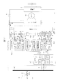
- FIG. 1 is an explanatory diagram showing an example of the configuration of the battery system according to Embodiment 1 of the present invention
- FIG. 2 is an explanatory diagram showing an example of the configuration of the battery monitoring AFE provided in the battery system of FIG. 1
- FIG. 4 is an explanatory diagram of a mechanism for reducing the power of the battery cell during charging
- FIG. 4 is an explanatory diagram of a mechanism for reducing the power of the battery cell during discharging (use)
- FIG. 5 is provided in the battery system of FIG.
- FIG. 6 is an explanatory diagram showing the principle of the balance circuit
- FIG. 6 is an explanatory diagram showing a modification of the balance circuit shown in FIG. 5, and FIG.
- FIG. 7 is an explanatory diagram showing another modification of the balance circuit shown in FIG. 8 is an explanatory diagram showing another modification of the balance circuit of FIG. 6, and
- FIG. 9 is an explanatory diagram showing an example of a specific circuit configuration of the balance circuit provided in the battery system of FIG. 10 is an explanatory diagram showing an example of the DC converter provided in the balance circuit of FIG. 9,
- FIG. 11 is an explanatory diagram showing an example of the pulse voltage generation circuit provided in the balance circuit of FIG. 9, and
- FIG. 9 is an explanatory diagram showing an example of the configuration of the DC step-down converter provided in the balance circuit
- FIG. 13 is a schematic diagram showing the DC converter of FIG. 9 and a part of the pulse voltage generation circuit of FIG. 11, and
- FIG. It is a timing chart of each part signal in FIG.
- the outline of the present embodiment is a battery (battery 2) configured by connecting a plurality of secondary battery cells (battery cells 2a) in series, and a battery control unit (balance circuit 4) that controls charging / discharging of the battery. , MCU5, battery monitoring AFE6).
- the battery control unit includes a battery monitoring unit (battery monitoring AFE 6) that monitors the secondary battery cells, and a cell balance circuit (balance circuit 4) that performs battery cell balance control.
- battery monitoring AFE 6 battery monitoring AFE 6
- cell balance circuit balance circuit
- the cell balance circuit is supplied with a second power supply voltage (power supply voltage VCC) obtained by stepping down the first power supply voltage (power supply voltage VBAT) supplied from the battery.
- a pulse generation circuit (pulse voltage generation circuit 31a, pulse signal generation circuit 31b) that generates a pulse signal is connected to the secondary battery cell, and the secondary battery cell is charged based on the pulse signal generated by the pulse generation circuit.
- a first DC converter that generates a charging voltage to be generated.
- a battery monitoring part specifies the secondary battery cell which charges based on the charge control signal (address information) which selects the secondary battery cell which charges, and the secondary battery cell is connected 1st
- An operation control signal (ON / OFF signal) is output to the DC converter, and the first DC converter charges the secondary battery cell by operating based on the operation control signal output from the battery monitoring unit. .
- the battery system 1 is a power supply system mounted on an automobile such as an EV or HEV, for example. As shown in FIG. 1, the battery system 1 includes a battery 2, a battery control unit 3, and a balance circuit 4.
- the battery 2 is a rechargeable secondary battery, and has a configuration in which, for example, about tens to hundreds of battery cells 2a having a rated voltage of about 3.6V are connected in series.
- the battery control unit 3 is a battery voltage control IC that performs various types of monitoring such as overcharge, overdischarge, and overcurrent in the battery 2 and battery protection.
- the MCU (Micro-Control Unit) 5 and a plurality of battery monitors It is comprised from AFE6.
- the MCU 5 and the battery monitoring AFE 6 are formed on, for example, individual semiconductor chips.
- the MCU 5 transmits a monitoring result of the battery cell 2a or receives a control signal of the battery system 1 through a CAN (Controller Area Network) described later.
- the battery monitoring AFE 6 is an IC for battery cell monitoring, and acquires battery cell monitoring information based on a command output from the MCU 5.
- the battery monitoring AFE 6 performs monitoring control of the battery cells 2a provided in one battery cell set 2b by, for example, one battery monitoring AFE.
- the battery cell set 2b has a configuration in which, for example, about 6 to 14 battery cells are connected in series.
- the monitoring information of the battery cell 2a acquired by each battery monitoring AFE 6 is transmitted to the MCU 5.
- the balance circuit 4 selectively charges an arbitrary battery cell 2a based on the control signal output from the battery monitoring AFE 6.
- the battery 2 has a positive (+) side electrode and a negative ( ⁇ ) side electrode.
- the power source of the battery 2 is connected so as to be supplied to a motor control unit 7 that controls an inverter that controls driving of a three-phase motor M mounted on an automobile such as an EV or HEV, and the balance circuit 4.
- the battery 2 is charged by a DC power source 8 as an external charger or a regenerative electric power from a running motor M.
- a positive (+) side electrode and a negative ( ⁇ ) Release energy from the side electrode When the motor M is driven, a positive (+) side electrode and a negative ( ⁇ ) Release energy from the side electrode.
- the MCU 5 communicates with an ECU (Electric control unit) 9 that controls the battery system 1.
- ECU Electronic control unit
- various ECUs that control various types of control such as a motor M, a power train system such as an engine, an information system such as a navigation system and an audio system, and a body system such as an air conditioner, a headlight, and a door lock. Many (not shown) are installed.
- the above-mentioned CAN is used as a communication network protocol for connecting the MCU 5 and the ECU 9.
- the MCU 5 is connected to the CAN bus Bc via the CAN transceiver / receiver 10.
- the ECU 9 is connected to the CAN bus Bc via the CAN transceiver / receiver 11.
- the other ECUs are similarly connected to the CAN bus Bc via a CAN transceiver / receiver (not shown).
- a CAN protocol differential signal is transferred to the CAN bus Bc.
- the CAN transceiver / receiver 10 converts the differential signal input via the CAN bus Bc into a digital signal and outputs it to the MCU 5, and also converts the digital signal output from the MCU 5 into a differential signal and converts it into the CAN bus Bc. Output to.
- the MCU 5 includes an SPI (Serial Peripheral Interface) 12, a CPU 13, a CAN interface 14, a memory 15, and the like.
- the SPI 12 is an interface that performs serial communication, and performs communication with the battery monitoring AFE 6 via the digital isolator DI.
- the CPU 13 controls the operation of the MCU 5.
- the CAN interface 14 is an interface between the MCU 5 and the CAN bus Bc.
- the memory 15 includes, for example, a RAM (Random Access Memory) or a ROM (Read Only Memory).
- the RAM is used as a work area for the CPU 13, for example.
- the ROM stores, for example, an operation program for the MCU 5.
- FIG. 2 is an explanatory diagram showing an example of the configuration of the battery monitoring AFE 6.
- It comprises an analog multiplexer 16, an A / D converter 17, SPIs 18 and 19, a register group 20, level shifters 21 and 22, a discharge control unit 23, a charge control signal output unit 23a, a regulator 24, and the like.
- the battery monitoring AFE 6 is provided with external terminals C12 to C0, B12 to B1, D12 to D1, SDO, SCLK, SSO and the like.
- the discharge control unit 23 includes a plurality of resistors R1 and a plurality of transistors T1.
- the charging control signal output unit 23a includes a plurality of resistors R2 and a plurality of transistors T2. These transistors T1 and T2 are composed of, for example, an N channel MOS (Metal Oxide Semiconductor).
- a resistor R1 and a transistor T1 in the discharge controller 23 are connected in series.
- a resistor R2 and a transistor T2 in the charge control signal output unit 23a are connected in series.
- a resistor R1 and a transistor T1 connected in series, and a resistor R2 and a transistor T2 connected in series are connected in parallel.
- the external terminals C11 to C0 have the same connection configuration.
- connection portions of the resistor R1 and the transistor T1 are connected to the external terminals D12 to D1, respectively, and the connection portions of the resistor R1 and the transistor T1 are connected to the external terminals B12 to B1, respectively.
- the battery cells 2a in the battery 2 are connected to the external terminals C12 to C0, respectively, and the discharging resistor Rr is connected to the external terminals D12 to D1, respectively.
- the external terminals B12 to B1 are connected to the balance circuit 4 so that control signals for controlling the operation of the balance circuit 4 are input to the balance circuit 4, respectively.
- the external terminal SDI is a terminal to which an external serial signal is input to the SPI 19
- the external terminal SCLKI is a terminal to which a synchronous clock of the serial signal is supplied to the SPI 19.
- the external terminal SSI is a terminal to which a select signal input to the SPI 19 is supplied.
- the external terminal SDO is a terminal that outputs a serial signal from the SPI 18 to the outside
- the external terminal SCLKO is a terminal that outputs a synchronous clock of the serial signal from the SPI 18 to the outside.
- the external terminal SSO is a terminal that outputs a select signal from the SPI 19.
- the analog multiplexer 16 is connected to the power supply voltage VCC.
- the power supply voltage VCC is a power supply voltage generated by a DC step-down converter 32 described later.
- the analog multiplexer 16 selects an arbitrary voltage value of the battery cell 2 a based on the selection signal, and outputs it to the A / D converter 17.
- the A / D converter 17 performs A / D conversion on the voltage value output via the analog multiplexer 16 and outputs it to the register group 20.
- the selection signal input to the analog multiplexer 16 is output from the ECU 9 and input to the control terminal of the analog multiplexer 16 via the SPI 19, the register group 20, and the A / D converter 17.
- the register group 20 is provided with a plurality of registers REG.
- the register group 20 temporarily stores digital data A / D converted by the A / D converter 17 or control data output from the ECU 9.
- the transistor T1 specified by the address information output from the ECU 9 is turned on, and the energy of the arbitrary battery cell 2a is discharged to the discharge resistor Rr connected externally.
- the register REG stores charging cell specifying information for specifying the battery cell 2a to be charged from the input address information.
- the charging cell specifying information is searched based on the address information output from the ECU 9, the transistor T2 specified by the search result is turned on, and a control signal is output to the balance circuit 4. Then, any battery cell 2 a is charged by the balance circuit 4.
- the regulator 24 steps down the power supply voltage VCC to generate a power supply voltage VREG (for example, about 5.0 V).
- the battery system 1 is controlled by the ECU 9 via the CAN bus Bc as described above.
- the MCU 5 that controls the battery 2 Upon receiving a request from the ECU 9, the MCU 5 that controls the battery 2 outputs an instruction to the battery monitoring AFE 6.
- the battery monitoring AFE 6 is daisy chain connected by the SPIs 18 and 19, and an instruction from the MCU 5 is transmitted by a serial signal.
- the voltage in each battery cell 2 a of the battery 2 is input to the A / D converter 17 through the analog multiplexer 16.
- the A / D converted voltage value is input to the ECU 9 via the register group 20, the SPI 18, and the MCU 5, and the ECU 9 measures the cell voltage of an arbitrary battery cell 2a. Which battery cell 2a outputs the voltage from the analog multiplexer 16 is determined by the selection signal output from the ECU 9 as described above.
- the ECU 9 In the cell balance control of the battery 2, when there is a battery cell that the ECU 9 determines that the cell voltage is high, the ECU 9 outputs an address signal for discharging the corresponding battery cell to the battery monitoring AFE by a serial signal.
- the battery monitoring AFE 6 searches the information stored in the register REG of the register group 20 based on the address signal output from the ECU 9, specifies a battery cell to be discharged, and outputs a signal for selecting the corresponding transistor T1. To do.
- the signal output from the register REG is input to the corresponding transistor T1 via the level shifter 21, and when the transistor T1 is turned on, the battery cell is selected via the external resistor Rr connected to the external terminal Dn. Discharged.
- the ECU 9 when the ECU 9 detects the battery cell 2a having a low cell voltage, the ECU 9 outputs address information so as to operate the balance circuit 4.
- the battery monitoring AFE 6 searches the charging cell specifying information stored in the register REG based on the address information output from the ECU 9, specifies any battery cell 2a to be charged, and corresponds to the specified battery cell 2a. A signal for selecting the transistor T2 is output.
- the signal output from the register REG is input to the corresponding transistor T2 via the level shifter 22.
- an ON / OFF signal is output to the balance circuit 4 via the external terminal Bn.
- the balance circuit 4 selectively charges an arbitrary battery cell based on the input ON / OFF signal.
- the battery cell has a maximum voltage and a minimum voltage that can be used, and must be used between them (referred to as operating voltage).
- FIG. 3A a battery in which battery cells CE1 to CE4 are connected in series is charged.
- FIG. 3B assuming that the discharge capacity of each battery cell has a relationship of CE3 ⁇ CE4 ⁇ CE1 ⁇ CE2, as shown in FIG.
- the voltage of the small battery cell CE3 rises quickly and quickly reaches the operating voltage upper limit. If this is left unattended, further charging will not be possible, and only the battery cells that have reached the operating voltage upper limit will not be fully charged.
- the battery (whole) cannot be discharged any more, but at this time, the other battery cells CE1, CE2, CE4 are still in a dischargeable state.
- the charging can be performed to almost all the battery cells. Further, not only when the battery 2 is charged but also when the battery 2 is used (during discharge), by using the balance circuit 4 to align the cell voltages, it is possible to discharge without waste.
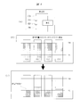
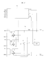
- FIG. 5 is an explanatory diagram showing the principle in the balance circuit 4 provided in the battery system 1.
- the balance circuit 4 includes a plurality of DC converters 25, a switching element 26, and a transformer 27, as shown.
- the DC converter 25 is connected to the positive (+) side electrode and the negative ( ⁇ ) side electrode of the battery cell 2a of the battery cell set 2b.
- the positive (+) side electrode of the battery cell set 2 b is connected to one end of the primary winding of the transformer 27, and the switching element 26 is connected to the other end of the primary winding of the transformer 27.
- One of the connection portions is connected.
- the other connection portion of the switching element 26 is connected to the negative ( ⁇ ) side electrode of the battery cell set 2b.
- the switching element 26 is turned on / off based on a pulse signal having a constant period.
- the transformer 27 is provided with a plurality of secondary windings, and these secondary windings are connected to the plurality of DC converters 25, respectively.
- the DC converter 25 is supplied with an induced voltage generated by the secondary winding of the transformer 27.
- each battery cell 2a in the battery cell set 2b is connected to the output portion of the DC converter 25, respectively.
- the DC converter 25 converts the voltage generated by the secondary winding of the transformer 27 into an arbitrary DC voltage and outputs it.
- These DC converters 25 are each controlled in operation based on an ON / OFF signal output from the battery monitoring AFE 6.
- the switch is turned on / off (switched) with a constant cycle and a constant pulse width as described above.
- the polarity of the secondary winding of the transformer 27 depends on the type of converter connected to the battery cell 2a.
- a forward type transformer In the case of a forward type transformer, it has the same polarity as that of the primary winding, and in the case of a flyback type transformer, it has a reverse polarity.
- a forward type or a flyback type in a narrow sense will be described, but not limited to this, various power source types are possible.
- the forward type naturally includes a push-pull, half-bridge, full-bridge type, and the like
- the flyback type naturally includes an RCC (ringing choke inverter) type.
- the DC converter 25 is a so-called mag-amplifier converter that has at least one saturable inductor and can control the pulse width of the secondary voltage according to the characteristics thereof.
- the output voltage of the DC converter 25 is controlled to be a certain constant voltage (usually near the maximum operating voltage of the battery cell).
- the DC converter 25 operates when the ON / OFF signal output from the battery monitoring AFE 6 becomes active.
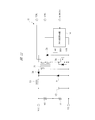
- FIG. 6 is an explanatory view showing a modification of the balance circuit 4 shown in FIG.
- the balance circuit 4 shown in FIG. 5 has a configuration in which one transformer 27 is provided, but in FIG. 6, the same number of transformers 27a as the number of battery cells 2a in the battery 2 are provided.
- the positive (+) side electrode of the battery 2 and one connection portion of the switching element 26 are connected to one end portion of the primary winding of the transformer 27a. Further, the negative ( ⁇ ) side electrode of the battery 2 is connected to the other connection portion of the switching element 26 and the other end portion of the primary winding of the transformer 27a.
- Other circuit configurations and connections are the same as those in FIG.
- the number of battery cells is several (for example, about 4 cells). Therefore, the number of battery cells becomes as large as about 96, for example.
- the transformer 27a when the transformer 27a is provided in the same number as the battery cell 2a, the number of secondary windings becomes one, and a transformer with excellent coupling can be obtained, and leakage inductance and the like are reduced. It can be greatly reduced.
- FIG. 7 is an explanatory view showing another modification of the balance circuit 4 shown in FIG.
- the balance circuit 4 shown in FIG. 7 has a configuration in which the switching element 26 is deleted from the configuration of the balance circuit 4 in FIG. 6 and a DC / AC converter 28 is newly provided.
- the DC / AC converter 28 is connected to the positive (+) side electrode and the negative ( ⁇ ) side electrode of the battery 2, and converts the DC voltage supplied from the battery 2 into an AC voltage for output.
- One end of the primary winding of the transformer 27a is connected to the output section of the DC / AC converter 28, and the other end of the primary winding of the transformer 27a is connected to the negative end of the battery 2.
- the ( ⁇ ) side electrodes are connected to each other. The other circuit configurations and connections are the same as in FIG.
- the DC / AC converter 28 generates an AC voltage from the power source (DC voltage) of the battery 2.
- the DC / AC converter 28 outputs an AC voltage waveform that is an optimum driving waveform to the DC converter 25.
- the DC / AC converter shown in FIG. 7 is also called an inverter, and there are various DC / AC conversion technologies. However, when converting to an AC voltage different from the input voltage, the DC / DC converter temporarily steps down to a desired voltage. After that, the DC / AC conversion is generally performed.
- FIG. 8 is an explanatory view showing another modification of the balance circuit 4 of FIG.
- a DC / DC converter 29 is newly provided in the configuration of the balance circuit 4 in FIG.
- the DC / DC converter 29 is connected to the positive (+) side electrode and the negative ( ⁇ ) side electrode of the battery 2, and converts the DC voltage supplied from the battery 2 into an arbitrary DC voltage and outputs it. To do.
- One end of the primary winding of the transformer 27a is connected to the output section of the DC / DC converter 29, and the other end of the primary winding of the transformer 27a is connected to the negative end of the battery 2.
- the ( ⁇ ) side electrodes are connected to each other.
- the other circuit configurations and connections are the same as in FIG.
- the DC / DC converter 29 that converts the voltage of the battery 2 into a DC voltage serves as a charging supply source for a large number of battery cells, for example, about 100 cells.
- the optimum switching frequency is often about several tens of kHz depending on the power source. Further, the DC converter 25 is low power because it is sufficient to charge only one battery cell.
- the switching frequency in the switching element 26 is preferably about 100 kHz or more.
- the DC / DC converter 29 can supply the optimum frequency, pulse width, and voltage to the DC converter 25.
- the degree of freedom can be increased, and the efficiency can be improved and the cost can be reduced.
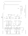
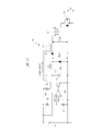
- FIG. 9 is an explanatory diagram illustrating an example of a specific circuit configuration of the balance circuit 4.
- the battery system 1 is provided with eight battery monitoring AFEs 6 and the total number of battery cells of the battery 2 is 96. Therefore, 12 battery cells 2a are monitored by one battery monitoring AFE6.
- the voltage of the battery cell set 2b is about 43.2V.
- the balance circuit 4 is connected to the upper and lower three battery cells 2 a among the twelve battery cells 2 a constituting one battery cell set 2 b connected to one battery monitoring AFE 6. The structure of the part is shown.
- the balance circuit 4 includes a plurality of DC converters 30, a pulse voltage generation unit 31, and a DC step-down converter 32.
- the positive (+) side electrode of each battery cell 2a is connected to the output terminal BCP of the DC converter 30, and the negative ( ⁇ ) side electrode of each battery cell 2a is connected to the output terminal BCN of the DC converter 30. Each is connected.
- control terminal EBL_B provided in the DC converter 30 is connected so that an ON / OFF signal output from the battery monitoring AFE 6 is input.
- This ON / OFF signal is a control signal for controlling the operation of the DC converter 30.
- the DC converter 30 operates or stops based on the ON / OFF signal as described above.
- the pulse voltage generation unit 31 includes a plurality of pulse voltage generation circuits 31a and a pulse signal generation circuit 31b.
- the pulse voltage generation circuit 31a generates a DC voltage based on the pulse signal generated by the pulse signal generation circuit 31b.
- the DC voltage generated by the pulse voltage generation circuit 31a is supplied to each DC converter 30.
- the DC step-down converter 32 is supplied with the voltage VBATT supplied via the terminal VIN1 and the power supply voltage VREG generated by the regulator 24 via the terminal VIN2.
- This step-down DC converter 32 steps down the voltage VBATT to generate the power supply voltage VCC.
- the voltage VBATT is a power supply voltage supplied from the battery cell set 2b connected to one battery monitoring AFE.
- the generated power supply voltage VCC is supplied to each pulse voltage generation circuit 31a via a terminal VOUT1 of the DC step-down converter 32 and a terminal VIN3 provided in the pulse voltage generation circuit 31a.
- the pulse signal generation circuit 31b is composed of an oscillation circuit such as an oscillator, for example, and generates a pulse signal having an arbitrary period and outputs it to the pulse signal input terminal IN of the pulse voltage generation circuit 31a.
- the pulse voltage generation circuit 31a generates a pulse voltage based on the pulse signal generated by the pulse signal generation circuit 31b, and supplies the pulse voltage generated from the output terminals PO3 to PO1 via the input part PIN of the DC converter 30, respectively. To do.
- FIG. 10 is an explanatory diagram showing an example of the DC converter 30 provided in the balance circuit 4 of FIG.
- the DC converter 30 includes resistors R1 to R4, an operational amplifier OP1, transistors T1 and T2, capacitors C1, diodes D1 and D2, an inductor L1, and a saturable inductor L2.
- the transistor T1 is made of, for example, a PNP bipolar transistor, and the transistor T2 is made of an NPN bipolar transistor.
- An input terminal PIN is connected to one end of the saturable inductor L2, and an anode of the diode D2 and a collector of the transistor T1 are connected to the other end of the saturable inductor L2. .
- the cathode of the diode D2 is connected to the cathode of the diode D1 and the other end of the inductor L1, which is a choke coil.
- One connection portion of the capacitor C1 and the output terminal BCP are connected to the other connection portion of the inductor L1, respectively.
- the base of the transistor T1 is connected to the collector of the transistor T2 and one connection portion of the resistor R4.
- the other connection portion of the resistor R4, one connection portion of the resistor R2, and the output terminal BCP are connected to the emitter of the transistor T1, respectively.
- connection part of the resistor R3 is connected to the other connection part of the resistor R2, and the positive (+) side input terminal of the operational amplifier OP1 and one of the resistors R1 are connected to the connection part of these resistors R2 and R3. Are connected to each other.
- a control terminal EBL_B is connected to the other connection portion of the resistor R1.
- the reference voltage VREF is input to the negative ( ⁇ ) side input terminal of the operational amplifier OP1, and the base of the transistor T2 is connected to the output terminal of the operational amplifier OP1.
- a shunt regulator is configured by the operational amplifier OP1 in which the reference voltage VREF is input to the negative ( ⁇ ) side input terminal and the transistor T2.
- the output terminal BCN is connected to the anode of the diode D1, the other connection of the capacitor C1, the emitter of the transistor T2, and the other connection of the resistor R3.
- FIG. 11 is an explanatory diagram showing an example of the pulse voltage generation circuit 31a provided in the balance circuit 4 of FIG.
- the pulse voltage generation circuit 31a includes three transformers 33, three transistors T3 made of N-channel MOS, three diodes D3, and a buffer B1. One end of the primary winding of the transformer 33 and the buffer B1 are connected so that the power supply voltage VCC is supplied.
- one end of the transistor T3 and the cathode of the diode D3 are connected to the other end of the primary winding of the transformer 33, respectively.
- the reference potential VSS is connected to the other connection portion of the transistor T3 and the anode of the diode D3.
- the input of the buffer B1 is connected so that the pulse signal generated by the pulse signal generation circuit 31a is input via the pulse signal input terminal IN.
- the output of the buffer B1 is connected to the gate of the transistor T3.
- Output sections PO3 to PO1 are connected to one end of the secondary winding of the transformer 33, and output sections BCN3 to BCN1 are connected to the other end of the secondary winding of the transformer 33, respectively. Has been.
- the output terminal PO and the output terminal BCN of the pulse voltage generation circuit 31a are respectively connected to the input terminal PIN and the input terminal BCN of the DC converter 30, and the DC voltage generated by the pulse voltage generation circuit 31a is supplied to the DC converter 30. Connected to be supplied.
- FIG. 12 is an explanatory diagram showing an example of the configuration of the DC step-down converter 32 provided in the balance circuit 4 of FIG.
- the DC step-down converter 32 includes a PWM control unit 34, diodes D6 to D9, an inductor L3, a transistor T6, a capacitor C2, resistors R6 and R5, and a transformer 35.
- the transistor T6 includes, for example, an N-channel MOSFET (Metal / Oxide / Semiconductor / Field / Effect / Transistor).
- a terminal VOUT1 is connected to one connection part of the resistor R6, one connection part of the capacitor C2, and one end part of the inductor L3, and the power supply voltage VCC purified by the DC step-down converter 32 via the terminal VOUT1. Is output.
- connection part of the resistor R5 is connected to the other connection part of the resistor R6, and the reference potential VSS is connected to the other connection part of the resistor R5.
- the cathodes of the diodes D8 and D9 are connected to the other end of the inductor L3.
- One end of the primary winding of the transformer 35 is connected to the anode of the diode D8.
- a cathode of a diode D6 is connected to one end of the secondary winding of the transformer 35, and a terminal VIN1 is connected to a midpoint of the secondary winding of the transformer 35.
- the power supply voltage VBAT supplied from the battery cell 2 is connected to the terminal VIN1.
- One end of the transistor T6 and the cathode of the diode D1 are connected to the other end of the secondary winding of the transformer 35, respectively.
- the gate of the transistor T6 is connected to the output unit of the PWM control unit 34, and the transistor T6 performs an on / off (switching) operation based on the PWM signal DRV output from the PWM control unit 34.
- the PWM control unit 34 is supplied with the power supply voltage VREG generated by the regulator 24 as an operating power supply via the terminal VIN2.
- the control terminal REMOTE of the PWM control unit 34 is connected so that a control signal from the MCU 5 is input, and the PWM control unit 34 operates based on this control signal.
- control terminal REMOTE for example, by outputting a control signal for stopping the operation from the MCU 5 (or the battery monitoring AFE), when the cell balance (charging the battery cell) is unnecessary, the DC step-down converter Therefore, the current consumption can be reduced and the dischargeable time can be increased.
- connection part between the resistor R4 and the resistor R5 is connected to the feedback terminal FB of the PWM control unit 34.
- the PWM control unit 34 varies the duty of the PWM signal DRV so that the voltage level of the power supply voltage VCC becomes substantially constant from the voltage generated by the resistance voltage division by the resistors R4 and R5.
- the power supply supplied to the terminal VIN2 may be other than the power supply voltage VREG.
- the power supply is directly supplied from the battery cell set 2b, self-supplied with a dedicated winding in the transformer 35, or a dedicated power source called AUX or the like. It may be supplied by a small auxiliary power source or the like.
- the DC step-down converter 32 includes a forward converter as shown in FIG.
- the PWM control unit 34 operates and a PWM signal is output.
- the transistor T6 is turned on (conducted) based on the PWM signal, a forward bias is applied to the diode D8, a current flows toward the inductor L3, and electric energy is stored in the inductors L3 and C2, and at the same time a load is applied to VCC. Supply current.
- the transistor T6 when the transistor T6 is turned off (cut off), the back electromotive force of the inductor L3 causes reflux to the diodes D8 and D9, and the current value of the inductor L3 decreases, but the load current continues to be supplied to VCC.
- the transistor T6 again before the current value of the inductor L3 becomes zero, the current starts to flow again through the inductor L3, and the DC step-down converter 32 enters the operation mode and generates the power supply voltage VCC.
- the power supply voltage VCC generated by the DC step-down converter 32 is supplied to the pulse voltage generation circuit 31a of FIG.
- each transistor T3 is turned on / off (switched) based on the pulse signal generated by the pulse signal generation circuit 31b, and the pulse signal generated on the secondary winding side of the transformer 33 is converted to DC.
- Each is supplied to the converter 30.
- the secondary winding of the transformer 33 is connected to the saturable inductor L2.
- the saturable inductor L2 utilizes the characteristic that the inductance value of the coil is large at a current below a certain value, and that the coil inductance approaches zero as much as at a current above a certain value. Change.
- the connection configuration after the saturable inductor L2 is a so-called mag-amplifier type forward converter.
- the switching frequency is preferably about 40 kHz, for example.
- the winding ratio of the transformer 35 in the DC converter 30 that is a mag-amplifier forward converter is set to, for example, about 20 V in consideration of the gate breakdown voltage of the transistor T6 and the like.
- the switching frequency of the transistor T6 is set to, for example, about 100 kHz in order to reduce the size of the transformer 35 and the saturable inductor L2. Since the winding ratio of the transformer 35 is 2: 1, for example, the peak value on the secondary side is approximately 10V.
- the pulse width (primary ON time) is about 5 ⁇ s with a margin.
- the resistors R1 to R3 are divided by the resistor R1 and the combined resistance of the resistor R2 and the resistor R3 when the ON / OFF signal output from the battery monitoring AFE6 is at the Lo level (charging the battery cell). For example, when the voltage is set to about 4.2 V and the ON / OFF signal is at the Hi level (charging to the battery cell is stopped), the voltage is set to about 1.5 V, for example.
- FIG. 13 is a schematic diagram showing the DC converter 30 and a part of the pulse voltage generation circuit 31a.
- the gate voltage VG of the transistor T3 the voltage V2nd between the secondary windings of the transformer 33, and the voltage dividing resistor (hereinafter referred to as voltage VINP) between the resistor R2 and the resistor R3 are the reference.
- the voltage VREC between the diodes D1 when the voltage is lower than the voltage VREF, the voltage VREC when the voltage VINP and the reference voltage VREF are substantially equal, and the voltage VREC when the voltage VINP is higher than the reference voltage VREF are shown.
- the ECU 9 When it is determined that there is a battery cell that needs to be charged, the ECU 9 outputs address information to the battery monitoring AFE 6 via the MCU 5. In the corresponding battery monitoring AFE 6, the transistor T 2 specified by the address information is turned on and a Lo level ON / OFF signal is output to the balance circuit 4, and any battery cell is charged by the balance circuit 4.
- the battery cell when the rated voltage of the battery cell is 3.6V, the battery cell is charged when the cell voltage is less than about 4.2V.
- the voltage VINP input to the positive (+) side input terminal of the operational amplifier OP1 becomes lower than the reference voltage VREF. Therefore, the output of the operational amplifier OP1 is at the Lo level. Is output.
- the output of the operational amplifier OP1 becomes Hi level. Due to this Hi level signal, the transistor T2 and the transistor T1 are turned on, respectively, and current flows through the transistor T1 to the saturable inductor L2 side.
- the operational amplifier OP1 when the ON / OFF signal is Hi level, the operational amplifier OP1 has a set voltage of 1.5V (voltage VINP), and the minimum voltage of the battery cell is, for example, about 2.0V in a normal use state. Therefore, a Hi level signal is always output (FIG. 14, VINP >> VREF). Therefore, since the saturable inductor L2 is continuously reset, charging is not performed.
- the DC converter 30 composed of the converter of the mag amplifier type, it becomes possible to easily perform the charge control by the ON / OFF signal output from the battery monitoring AFE 6 and charge the battery cell having a low voltage. It can be done in a short time.
- the ON / OFF signal is a signal at the DC level and the switch control of the DC converter 30 is not performed, the ON / OFF signal does not become a noise generation source to the battery monitoring AFE, and the reliability can be improved. .
- the battery cell Since the maximum voltage generated by the DC converter 30 is managed and controlled by the saturable inductor L2, the operational amplifier OP1, and the reference voltage VREF, the battery cell which is a problem of the active cell balance method by the converter of Non-Patent Document 1 described above. It also solves the management of working pressure voltage.
- the balance circuit 4 can be configured at low cost.
- each DC converter 30 has a battery cell close to the maximum operating voltage. Stops automatically when charged.
- any battery cell 2a can be efficiently charged in a short time by the balance circuit 4, so that the effective utilization rate of the discharge capacity of the battery cell 2a can be improved. it can.
- the cruising distance in the EV or HEV can be extended, and the life of the battery 2 can be extended.
- balance circuit 4 can be operated only by the ON / OFF signal according to an instruction from the ECU 9, a highly reliable active balance circuit 4 can be realized at low cost.
- FIG. 15 is an explanatory diagram showing an example of a DC converter provided in the balance circuit according to the second embodiment of the present invention.
- the battery cell is always in a discharged state.
- the resistors R1 to R3 and the operational amplifier OP1 are separated from the battery cell, and the discharge path is cut off.
- the DC converter 30 has a configuration in which transistors T7 to T10 and diodes D10 to D12 are newly added to the DC converter 30 shown in FIG.
- the transistors T7 to T9 are made of, for example, a P-channel MOS, and the transistor T10 is made of, for example, an NPN-type bipolar transistor.
- the output part BCP is connected to one connection part of the transistors T7 and T8, respectively, and one connection part of the transistor T9 and one connection part of the resistor R1 are connected to the other connection part of the transistor T8, respectively. It is connected.
- the gates of the transistors T8 and T9 and the collector of the transistor T10 are connected to the other connection part of the resistor R1, respectively.
- the other connection part of the transistor T7 is connected to the base of the transistor T10, and the output part BCN is connected to the emitter of the transistor T10.
- diodes D10 to D12 are connected to the transistors T7 to T9, respectively, and these are all built-in diodes of the MOSFET.
- One end of inductor L1, one connection of capacitor C1, one connection of resistors R2 and R4, and the emitter of transistor T1 are connected to the other connection of transistor T9.
- the other resistors R1 to R4, operational amplifier OP1, transistors T1 and T2, capacitor C1, diodes D1 and D2, inductor L1, and saturable inductor L2 are connected in the same manner as in FIG. 10 of the first embodiment. The description is omitted.
- the current consumption of the balance circuit 4 can be made substantially zero.
- the transistors T7 to T10 are provided with the ON / OFF signal set to Lo active. However, if the ON / OFF signal is set to Hi active, the number of transistors can be simplified.
- the discharge of the battery cell passing through the balance circuit can be made substantially zero, so that the battery cell life can be reduced. Can be extended.
- FIG. 16 is an explanatory diagram showing an example of the configuration of the DC converter provided in the balance circuit according to the third embodiment of the present invention.
- the DC converter 30 is a mag-amp converter, but in the third embodiment, the DC converter 30 is a flyback type.
- the DC converter 30 has a configuration in which the inductor L1 and the diode D1 are omitted from the DC converter 30 of FIG.
- Other circuit configurations are the same as those in FIG.
- the energy flowing into the primary winding of the transformer and the energy output from the secondary winding are in opposite phases. Therefore, the polarity of the transformer 33 connected to the DC converter 30 is connected in reverse.
- the flyback type can reduce the area of the balance circuit 4 and reduce the cost.
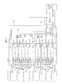
- FIG. 17 is an explanatory diagram showing an example of a specific circuit configuration of the battery system according to the fourth embodiment of the present invention
- FIG. 18 is an explanatory diagram showing a modification of FIG.
- the MCU 5 that receives the instruction to start the operation via the CAN bus Bc turns on the photocoupler PC1 via the I / O port.
- the output of the photocoupler PC1 is input as a standby signal to the standby terminal STBY of the battery monitoring AFE 6 via the resistor R20, whereby the battery monitoring AFE 6 is activated.
- the battery monitoring AFE 6 has a threshold value in the vicinity of the power supply voltage VCC-2.5V, stops operation when the voltage of the standby signal input to the standby terminal STBY becomes equal to or higher than the threshold voltage, and is lower than the threshold voltage Operates with voltage.
- the photocoupler PC2 is responsible for the insulation of the remote input of the PWM control unit 34. When the photocoupler PC2 is off, the collector potential (output) of the photocoupler PC2 is connected to the positive electrode of the fourth battery cell 2a from the bottom in the figure, and becomes that potential.
- the PWM control unit 34 maintains the stopped state regardless of whether the power is supplied.
- the transistor T20 which is an N-channel MOS, is turned on, and the transistor T21 is turned off in order to reduce the gate voltage of the transistor T21, which is also an NPN bipolar transistor.
- the main part of the current consumption at this time is the fourth part which is the off-leakage (leakage) current of the switching transistor T6, the base-collector resistance of the transistor T21 and its power supply. And the current corresponding to the voltage of the battery cell 2a.
- the off-reel current of the transistor T6 is about 100 nA
- the base-collector resistance of the transistor T21 is the hFE (DC current) of the transistor T21 when the minimum voltage of the fourth battery cell is 8V and the maximum voltage is about 16.8V.
- the amplification factor is 10,000 and the starting current of the PWM controller 34 is about 300 ⁇ A
- 30 nA can be passed at the time of 8 V of the minimum operating voltage, and 63 nA even at 16.8 V (in this case, the resistance value is 133 M ⁇ )
- the maximum is 840 nA with a margin of 20 M ⁇ , and can be about 1 ⁇ A or less.
- the output of the photocoupler PC2 becomes Lo level, and a Hi level control signal is input to the control terminal REMOTE of the PWM controller 34 via the inverter INV1.
- VSTAT the operable power supply voltage supplied to the PWM control unit 34
- this voltage is referred to as VSTAT.
- the transistor T20 since the transistor T20 is turned off, the base current is supplied to the transistor T21 to be turned on, and VSTAT is supplied to the PWM control unit 34. As a result, the PWM control unit 34 is activated and starts operating.
- the voltage level of the power supply voltage VCC output from the DC step-down converter 32 rises, and at the same time, the power supply of the PWM control unit 34 is supplied via the transformer 35 and the diode D8.
- the Zener diode ZD1 and the transistor T22 which is a PNP bipolar transistor, are turned on, so that the transistor T23, which is an N-channel MOS, is turned on.
- the power supply from the fourth battery cell is stopped (only the current due to the base-collector resistance of the transistor T21 described above), and the diode D8 is turned on. Only the supply from the transformer 35 is provided. Thereby, it is possible to prevent unnecessary current from being drawn from the middle of the battery cell.
- the battery system 1 is connected to the CAN bus Bc via the CAN transceiver / receiver 10 and is controlled by the ECU 9.
- the circuit for generating the standby signal described above (the circuit indicated by the two-dot chain line in the figure) has a configuration in which the battery monitoring AFE 6 and the MCU 5 are insulated.
- the DC step-down converter 32 and the MCU 5 are insulated. .
- a digital associator DI that is a circuit that performs signal insulation, and is insulated.
- the MCU 5 that operates with another power source for example, 12V system power source
- the battery system 1 that operates with the power source system of the battery 2 can be electrically insulated, and a failure due to a short circuit of the other power source is prevented. And reliability can be improved.
- FIG. 18 is an explanatory diagram showing an example of a specific circuit configuration of the battery system according to the fifth embodiment of the present invention.
- the outline of the present embodiment is a battery (battery 2) configured by connecting a plurality of secondary battery cells (battery cells 2a) in series, and a battery control unit (balance circuit 4) that controls charging / discharging of the battery. , MCU5, battery monitoring AFE6).
- the battery control unit includes a battery monitoring unit (battery monitoring AFE6) that monitors the secondary battery cells, and a cell balance circuit (balance circuit 4) that performs battery cell balance control.
- a pulse generation circuit which is supplied with a second power supply voltage (power supply voltage VCC) obtained by stepping down a first power supply voltage (power supply voltage VBAT) supplied from a battery, and generates a pulse signal having an arbitrary period from the second power supply voltage (Pulse voltage generation circuit 31a, pulse signal generation circuit 31b) are connected between the highest potential electrode and the lowest potential electrode in any number of secondary battery cells connected in series, thereby generating a pulse generation circuit.
- a first DC converter that generates a charging voltage for charging any number of secondary battery cells together based on the pulse signal.
- a battery monitoring part specifies the arbitrary number of secondary battery cells connected in series based on a charge control signal (address information), and the arbitrary number of secondary battery cells are connected.
- An operation control signal (ON / OFF signal) is output to the first DC converter, and the first DC converter operates based on the operation control signal and charges an arbitrary number of secondary battery cells. is there.
- the individual battery cells are shown as being charged by the balance circuit 4. However, for example, as shown in FIG. 18, a plurality of battery cells may be charged together.
- ⁇ Manufacturing variation is the main factor in battery cell variation, but it is not difficult to have the same characteristics if it is only a few cells. In that case, the loss does not increase so much even if the battery cell is subjected to passive cell balancing.
- a passive cell balance circuit is connected to each battery cell.
- the DC converter 30 in the balance circuit 4 is configured to charge, for example, four battery cells as a group.
- the set voltage for stopping the charging is set to about 16.8 V (4.2 V ⁇ 4) and the winding ratio of the transformer 33 is changed. Is also necessary.
- the present invention is suitable for cell balance control technology in a battery system used for EVs, HEVs, and the like.
Landscapes
- Engineering & Computer Science (AREA)
- Power Engineering (AREA)
- Transportation (AREA)
- Mechanical Engineering (AREA)
- Life Sciences & Earth Sciences (AREA)
- Sustainable Development (AREA)
- Sustainable Energy (AREA)
- Charge And Discharge Circuits For Batteries Or The Like (AREA)
- Secondary Cells (AREA)
- Electric Propulsion And Braking For Vehicles (AREA)
Abstract
Description
図1は、本発明の実施の形態1によるバッテリシステムにおける構成の一例を示す説明図、図2は、図1のバッテリシステムに設けられた電池監視AFEにおける構成の一例を示す説明図、図3は、充電時におけるバッテリセルの電力減少するメカニズムの説明図、図4は、放電(使用)時におけるバッテリセルの電力減少するメカニズムの説明図、図5は、図1のバッテリシステムに設けられたバランス回路における原理を示す説明図、図6は、図5に示したバランス回路における変形例を示した説明図、図7は、図6に示したバランス回路における他の変形例を示した説明図、図8は、図6のバランス回路の他の変形例を示した説明図、図9は、図1のバッテリシステムに設けられたバランス回路の具体的な回路構成の一例を示す説明図、図10は、図9のバランス回路に設けられたDCコンバータにおける一例を示す説明図、図11は、図9のバランス回路に設けられたパルス電圧発生回路における一例を示す説明図、図12は、図9バランス回路に設けられたDC降圧コンバータにおける構成の一例を示す説明図、図13は、図9のDCコンバータと図11のパルス電圧発生回路の一部とを示した概略図、図14は、図13における各部信号のタイミングチャートである。 (Embodiment 1)
1 is an explanatory diagram showing an example of the configuration of the battery system according to
本実施の形態の概要は、複数の二次電池セル(バッテリセル2a)を直列に接続して構成されたバッテリ(バッテリ2)と、該バッテリの充放電を制御するバッテリ制御部(バランス回路4、MCU5、電池監視AFE6)とを有したバッテリシステム(バッテリシステム1)に適用される。 <Outline of the embodiment>
The outline of the present embodiment is a battery (battery 2) configured by connecting a plurality of secondary battery cells (
本実施の形態1において、バッテリシステム1は、例えば、EVやHEVなどの自動車に搭載される電源システムである。バッテリシステム1は、図1に示すように、バッテリ2、電池制御部3、およびバランス回路4から構成されている。 <Example of battery system configuration>
In the first embodiment, the
図2は、電池監視AFE6における構成の一例を示す説明図である。 <Configuration example of battery monitoring AFE>
FIG. 2 is an explanatory diagram showing an example of the configuration of the
バッテリシステム1における動作例について説明する。 <Operation example of
An operation example in the
バッテリセルのセル電圧を揃える(セルバランス)理由について説明する。 <Reason for cell balance>
The reason why the cell voltages of the battery cells are aligned (cell balance) will be described.
図5は、バッテリシステム1に設けられたバランス回路4における原理を示す説明図である。 <Principle circuit example of balance circuit>
FIG. 5 is an explanatory diagram showing the principle in the
図9は、バランス回路4の具体的な回路構成の一例を示す説明図である。 <Example of specific balance circuit applied to battery system>
FIG. 9 is an explanatory diagram illustrating an example of a specific circuit configuration of the
DC降圧コンバータ32は、図12に示したように、フォーワードコンバータからなる。制御端子REMOTEを介してMCU5からの制御信号が入力されると、PWM制御部34が動作を行い、PWM信号が出力される。PWM信号に基づいて、トランジスタT6がオン(導通)すると、ダイオードD8に順方向バイアスがかかり、電流がインダクタL3に向かって流れ、該インダクタL3、C2に電気エネルギが蓄積されると同時にVCCに負荷電流を供給する。 <Operation of balance circuit>
The DC step-
以下、DCコンバータ30の動作について、図13の説明図、および図14のタイミングチャートを用いて説明する。 <Operation of DC converter>
Hereinafter, the operation of the
図15は、本発明の実施の形態2によるバランス回路に設けられたDCコンバータの一例を示す説明図である。 (Embodiment 2)
FIG. 15 is an explanatory diagram showing an example of a DC converter provided in the balance circuit according to the second embodiment of the present invention.
図16は、本発明の実施の形態3によるバランス回路に設けられたDCコンバータの構成の一例を示す説明図である。 (Embodiment 3)
FIG. 16 is an explanatory diagram showing an example of the configuration of the DC converter provided in the balance circuit according to the third embodiment of the present invention.
図17は、本発明の実施の形態4によるバッテリシステムの具体的な回路構成の一例を示す説明図、図18は、図17の変形例を示す説明図である。 (Embodiment 4)
FIG. 17 is an explanatory diagram showing an example of a specific circuit configuration of the battery system according to the fourth embodiment of the present invention, and FIG. 18 is an explanatory diagram showing a modification of FIG.
本実施の形態4では、バッテリシステム1の具体的な回路構成の一例を図17に示す。基本的な構成は、前記実施の形態1の図1と同様であるので、図17に示すバッテリシステム1の特徴的な点のみを以下に挙げる。 <Characteristics of battery system>
In the fourth embodiment, an example of a specific circuit configuration of the
図18は、本発明の実施の形態5によるバッテリシステムの具体的な回路構成の一例を示す説明図である。 (Embodiment 5)
FIG. 18 is an explanatory diagram showing an example of a specific circuit configuration of the battery system according to the fifth embodiment of the present invention.
本実施の形態の概要は、複数の二次電池セル(バッテリセル2a)を直列に接続して構成されたバッテリ(バッテリ2)と、該バッテリの充放電を制御するバッテリ制御部(バランス回路4、MCU5、電池監視AFE6)とを有するバッテリシステム(バッテリシステム1)に適用される。 <Outline of the embodiment>
The outline of the present embodiment is a battery (battery 2) configured by connecting a plurality of secondary battery cells (
2 バッテリ
2a バッテリセル
2b バッテリセル組
3 電池制御部
4 バランス回路
5 MCU
6 電池監視AFE
7 モータ制御部
8 DC電源
9 ECU
10 CANトランシーバ/レシーバ
11 CANトランシーバ/レシーバ
12 SPI
13 CPU
14 CANインタフェース
15 メモリ
16 アナログマルチプレクサ
17 A/D変換器
18 SPI
19 SPI
20 レジスタ群
21 レベルシフタ
22 レベルシフタ
23 放電制御部
23a 充電制御信号出力部
24 レギュレータ
25 DCコンバータ
26 スイッチング素子
27 トランス
27a トランス
28 DC/ACコンバータ
29 DC/DCコンバータ
30 DCコンバータ
31 パルス電圧発生部
31a パルス電圧発生回路
31b パルス信号発生回路
32 DC降圧コンバータ
33 トランス
34 PWM制御部
35 トランス
M モータ
Bc CANバス
OP1 オペアンプ
C1 コンデンサC2
D1 ダイオード D2D3D6D8D10
L1 インダクタ
L2 可飽和インダクタ
L3 インダクタ
REG レジスタ
R1~R6 抵抗
R20 抵抗
Rr 抵抗
T1~T3 トランジスタ
T6~T10 トランジスタ
T20~T23 トランジスタ
CE1~CE4 バッテリセル
B1 バッファ
PC1 フォトカプラ
PC2 フォトカプラ
INV1 インバータ
ZD1 ツェナーダイオード
DI デジタルアソレータ DESCRIPTION OF
6 Battery monitoring AFE
7
10 CAN transceiver /
13 CPU
14 CAN interface 15
19 SPI
20
D1 Diode D2D3D6D8D10
L1 Inductor L2 Saturable inductor L3 Inductor REG Resistor R1 to R6 Resistor R20 Resistor Rr Resistor T1 to T3 Transistor T6 to T10 Transistor T20 to T23 Transistor CE1 to CE4 Battery cell B1 Buffer PC1 Photocoupler PC2 Photocoupler INV1 Inverter ZD1 Zener diode DI Digital Assulator
Claims (16)
- 複数の二次電池セルを直列に接続して構成されたバッテリと、前記バッテリの充放電を制御するバッテリ制御部とを有するバッテリシステムであって、
前記バッテリ制御部は、
前記二次電池セルを監視する電池監視部と、
前記バッテリのセルバランス制御を行うセルバランス回路とを有し、
前記セルバランス回路は、
前記バッテリから供給される第1の電源電圧を降圧した第2の電源電圧が供給され、前記第2の電源電圧から任意の周期のパルス信号を生成するパルス発生回路と、
前記二次電池セルにそれぞれ接続され、前記パルス発生回路が生成したパルス信号に基づいて、前記二次電池セルに充電する充電電圧を生成する第1のDCコンバータとを有し、
前記電池監視部は、
充電を行う二次電池セルを選択する充電制御信号に基づいて、充電を行う前記二次電池セルを特定し、前記二次電池セルが接続されている第1のDCコンバータに対して動作制御信号を出力し、
前記第1のDCコンバータは、
前記動作制御信号に基づいて動作し、前記二次電池セルに充電することを特徴とするバッテリシステム。 A battery system having a battery configured by connecting a plurality of secondary battery cells in series, and a battery control unit that controls charging and discharging of the battery,
The battery control unit
A battery monitoring unit for monitoring the secondary battery cell;
A cell balance circuit for performing cell balance control of the battery,
The cell balance circuit is:
A pulse generation circuit that is supplied with a second power supply voltage obtained by stepping down the first power supply voltage supplied from the battery, and generates a pulse signal having an arbitrary period from the second power supply voltage;
A first DC converter connected to each of the secondary battery cells and generating a charging voltage for charging the secondary battery cell based on a pulse signal generated by the pulse generation circuit;
The battery monitoring unit
Based on a charge control signal for selecting a secondary battery cell to be charged, the secondary battery cell to be charged is specified, and an operation control signal for the first DC converter to which the secondary battery cell is connected Output
The first DC converter includes:
A battery system that operates based on the operation control signal and charges the secondary battery cell. - 請求項1記載のバッテリシステムにおいて、
前記第1のDCコンバータは、
可飽和インダクタを有し、前記可飽和インダクタによってスイッチング用のトランジスタの動作制御を行うことにより、前記二次電池セルを充電する電圧を生成するマグアンプ式のフォーワードコンバータからなることを特徴とするバッテリシステム。 The battery system according to claim 1,
The first DC converter includes:
A battery comprising a saturable inductor, and comprising a magamp type forward converter that generates a voltage for charging the secondary battery cell by controlling the operation of a switching transistor by the saturable inductor. system. - 請求項1記載のバッテリシステムにおいて、
前記第1のDCコンバータは、
可飽和インダクタを有し、前記可飽和インダクタによってスイッチング用のトランジスタの動作制御を行うことにより、前記二次電池セルを充電する電圧を生成するマグアンプ式のフライバックコンバータからなることを特徴とするバッテリシステム。 The battery system according to claim 1,
The first DC converter includes:
A battery comprising a saturable inductor, and comprising a mag-amp flyback converter that generates a voltage for charging the secondary battery cell by controlling the operation of a switching transistor by the saturable inductor. system. - 請求項1記載のバッテリシステムにおいて、
前記パルス発生回路は、
スイッチング信号に基づいて、スイッチングを行うスイッチング素子と、
一次巻き線側に接続された前記スイッチング素子のオン/オフ動作に伴い、二次巻き線側にエネルギを伝達し、前記パルス信号を発生させるトランスとを有し、
前記トランスは、
前記第1のDCコンバータと同じ数の二次巻き線を有することを特徴とするバッテリシステム。 The battery system according to claim 1,
The pulse generation circuit includes:
A switching element that performs switching based on the switching signal;
A transformer for transmitting energy to the secondary winding side and generating the pulse signal in accordance with the on / off operation of the switching element connected to the primary winding side;
The transformer is
A battery system having the same number of secondary windings as the first DC converter. - 請求項1記載のバッテリシステムにおいて、
さらに、前記バッテリから供給される第1の電源電圧を降圧し、前記パルス発生回路に供給する第2の電源電圧を生成する第2のコンバータを有することを特徴とするバッテリシステム。 The battery system according to claim 1,
The battery system further comprises a second converter for stepping down the first power supply voltage supplied from the battery and generating a second power supply voltage supplied to the pulse generation circuit. - 請求項1項に記載のバッテリシステムにおいて、
前記電池監視部は、
充電を行う前記二次電池セルを特定する充電セル特定情報を格納する特定情報格納部を有し、
前記電池監視部は、
前記充電制御信号に基づいて、前記特定情報格納部に格納された充電セル特定情報を検索し、充電を行う前記二次電池セルを特定して前記制御信号を出力することを特徴とするバッテリシステム。 The battery system according to claim 1,
The battery monitoring unit
A specific information storage unit for storing charging cell specifying information for specifying the secondary battery cell to be charged;
The battery monitoring unit
A battery system that searches for charging cell specifying information stored in the specifying information storage unit based on the charging control signal, specifies the secondary battery cell to be charged, and outputs the control signal. . - 請求項6記載のバッテリシステムにおいて、
前記バッテリシステムは、
通信バスを介して前記バッテリ制御部と接続され、
前記電池監視部に入力される前記充電制御信号は、
前記通信バスを介して前記バッテリ制御部から出力される信号であることを特徴とするバッテリシステム。 The battery system according to claim 6, wherein
The battery system is
Connected to the battery control unit via a communication bus;
The charge control signal input to the battery monitoring unit is
The battery system is a signal output from the battery control unit via the communication bus. - 請求項7記載のバッテリシステムにおいて、
前記通信バスの通信プロトコルインタフェースは、
CANであることを特徴とするバッテリシステム。 The battery system according to claim 7, wherein
The communication protocol interface of the communication bus is:
A battery system characterized by being a CAN. - 複数の二次電池セルを直列に接続して構成されたバッテリと、前記バッテリの充放電を制御するバッテリ制御部とを有するバッテリシステムであって、
前記バッテリ制御部は、
前記二次電池セルを監視する電池監視部と、
前記バッテリのセルバランス制御を行うセルバランス回路とを有し、
前記セルバランス回路は、
前記バッテリから供給される第1の電源電圧を降圧した第2の電源電圧が供給され、前記第2の電源電圧から任意の周期のパルス信号を生成するパルス発生回路と、
直列接続された任意の数の前記二次電池セルにおける最高電位の電極と最低電位の電極との間にそれぞれ接続され、前記パルス発生回路が生成したパルス信号に基づいて、任意の数の前記二次電池セルを纏めて充電する充電電圧を生成する第1のDCコンバータとを有し、
前記電池監視部は、
充電を行う任意の数の前記二次電池セルを選択する充電制御信号に基づいて、充電を行う前記二次電池セルを特定し、任意の数の前記二次電池セルが接続されている第1のDCコンバータに対して動作制御信号を出力し、
前記第1のDCコンバータは、
前記動作制御信号に基づいて動作し、任意の数の前記二次電池セルに充電することを特徴とするバッテリシステム。 A battery system having a battery configured by connecting a plurality of secondary battery cells in series, and a battery control unit that controls charging and discharging of the battery,
The battery control unit
A battery monitoring unit for monitoring the secondary battery cell;
A cell balance circuit for performing cell balance control of the battery,
The cell balance circuit is:
A pulse generation circuit which is supplied with a second power supply voltage obtained by stepping down the first power supply voltage supplied from the battery, and generates a pulse signal having an arbitrary period from the second power supply voltage;
An arbitrary number of the second battery cells are connected between the highest potential electrode and the lowest potential electrode in any number of the secondary battery cells connected in series, and based on the pulse signal generated by the pulse generation circuit, A first DC converter that generates a charging voltage for charging the subsequent battery cells together,
The battery monitoring unit
Based on a charge control signal for selecting an arbitrary number of secondary battery cells to be charged, the secondary battery cells to be charged are identified, and an arbitrary number of the secondary battery cells are connected to the first Output an operation control signal to the DC converter
The first DC converter includes:
A battery system that operates based on the operation control signal and charges an arbitrary number of the secondary battery cells. - 請求項9記載のバッテリシステムにおいて、
前記第1のDCコンバータは、
可飽和インダクタを有し、前記可飽和インダクタによってスイッチング用のトランジスタの動作制御を行うことにより、前記二次電池セルを充電する電圧を生成するマグアンプ式のフォーワードコンバータからなることを特徴とするバッテリシステム。 The battery system according to claim 9, wherein
The first DC converter includes:
A battery comprising a saturable inductor, and comprising a magamp type forward converter that generates a voltage for charging the secondary battery cell by controlling the operation of a switching transistor by the saturable inductor. system. - 請求項9記載のバッテリシステムにおいて、
前記第1のDCコンバータは、
可飽和インダクタを有し、前記可飽和インダクタによってスイッチング用のトランジスタの動作制御を行うことにより、前記二次電池セルを充電する電圧を生成するマグアンプ式のフライバックコンバータからなることを特徴とするバッテリシステム。 The battery system according to claim 9, wherein
The first DC converter includes:
A battery comprising a saturable inductor, and comprising a mag-amp flyback converter that generates a voltage for charging the secondary battery cell by controlling the operation of a switching transistor by the saturable inductor. system. - 請求項9記載のバッテリシステムにおいて、
前記パルス発生回路は、
スイッチング信号に基づいて、スイッチングを行うスイッチング素子と、
一次巻き線側に接続された前記スイッチング素子のオン/オフ動作に伴い、二次巻き線側にエネルギを伝達し、前記パルス信号を発生させるトランスとを有し、
前記トランスは、
前記第1のDCコンバータと同じ数の二次巻き線を有することを特徴とするバッテリシステム。 The battery system according to claim 9, wherein
The pulse generation circuit includes:
A switching element that performs switching based on the switching signal;
A transformer for transmitting energy to the secondary winding side and generating the pulse signal in accordance with the on / off operation of the switching element connected to the primary winding side;
The transformer is
A battery system having the same number of secondary windings as the first DC converter. - 請求項9記載のバッテリシステムにおいて、
さらに、前記バッテリから供給される第1の電源電圧を降圧し、前記パルス発生回路に供給する第2の電源電圧を生成する第2のコンバータを有することを特徴とするバッテリシステム。 The battery system according to claim 9, wherein
The battery system further comprises a second converter for stepping down the first power supply voltage supplied from the battery and generating a second power supply voltage supplied to the pulse generation circuit. - 請求項9項に記載のバッテリシステムにおいて、
前記電池監視部は、
充電を行う前記二次電池セルを特定する充電セル特定情報を格納する特定情報格納部を有し、
前記電池監視部は、
前記充電制御信号に基づいて、前記特定情報格納部に格納された充電セル特定情報を検索し、充電を行う前記二次電池セルを特定して前記制御信号を出力することを特徴とするバッテリシステム。 The battery system according to claim 9, wherein
The battery monitoring unit
A specific information storage unit for storing charging cell specifying information for specifying the secondary battery cell to be charged;
The battery monitoring unit
A battery system that searches for charging cell specifying information stored in the specifying information storage unit based on the charging control signal, specifies the secondary battery cell to be charged, and outputs the control signal. . - 請求項14記載のバッテリシステムにおいて、
前記バッテリシステムは、
通信バスを介して前記バッテリ制御部と接続され、
前記電池監視部に入力される前記充電制御信号は、
前記通信バスを介して前記バッテリ制御部から出力される信号であることを特徴とするバッテリシステム。 The battery system according to claim 14, wherein
The battery system is
Connected to the battery control unit via a communication bus;
The charge control signal input to the battery monitoring unit is
The battery system is a signal output from the battery control unit via the communication bus. - 請求項15記載のバッテリシステムにおいて、
前記通信バスの通信プロトコルインタフェースは、
CANであることを特徴とするバッテリシステム。 The battery system according to claim 15, wherein
The communication protocol interface of the communication bus is:
A battery system characterized by being a CAN.
Priority Applications (6)
| Application Number | Priority Date | Filing Date | Title |
|---|---|---|---|
| EP11874606.4A EP2773014B1 (en) | 2011-10-28 | 2011-10-28 | Battery system |
| KR1020147010948A KR101865442B1 (en) | 2011-10-28 | 2011-10-28 | Battery system |
| US14/354,567 US9478995B2 (en) | 2011-10-28 | 2011-10-28 | Battery system |
| PCT/JP2011/074951 WO2013061461A1 (en) | 2011-10-28 | 2011-10-28 | Battery system |
| CN201180074346.0A CN103891094B (en) | 2011-10-28 | 2011-10-28 | Battery system |
| JP2013540592A JP5730401B2 (en) | 2011-10-28 | 2011-10-28 | Battery system |
Applications Claiming Priority (1)
| Application Number | Priority Date | Filing Date | Title |
|---|---|---|---|
| PCT/JP2011/074951 WO2013061461A1 (en) | 2011-10-28 | 2011-10-28 | Battery system |
Publications (1)
| Publication Number | Publication Date |
|---|---|
| WO2013061461A1 true WO2013061461A1 (en) | 2013-05-02 |
Family
ID=48167324
Family Applications (1)
| Application Number | Title | Priority Date | Filing Date |
|---|---|---|---|
| PCT/JP2011/074951 WO2013061461A1 (en) | 2011-10-28 | 2011-10-28 | Battery system |
Country Status (6)
| Country | Link |
|---|---|
| US (1) | US9478995B2 (en) |
| EP (1) | EP2773014B1 (en) |
| JP (1) | JP5730401B2 (en) |
| KR (1) | KR101865442B1 (en) |
| CN (1) | CN103891094B (en) |
| WO (1) | WO2013061461A1 (en) |
Cited By (8)
| Publication number | Priority date | Publication date | Assignee | Title |
|---|---|---|---|---|
| CN103904755A (en) * | 2014-04-23 | 2014-07-02 | 武汉市欧力普能源与自动化技术有限公司 | DC/DC converter circuit for one-way modular high-power battery equalization |
| CN103904754A (en) * | 2014-04-23 | 2014-07-02 | 武汉市欧力普能源与自动化技术有限公司 | DC/DC convertor circuit for bi-directional modular high-power battery equalization |
| WO2015151432A1 (en) * | 2014-04-04 | 2015-10-08 | Sony Corporation | Charging device, charging control method, electricity storage device, power storage device, power system, and electric vehicle |
| JP2016152649A (en) * | 2015-02-16 | 2016-08-22 | ソニー株式会社 | Power controller, power control method and power control system |
| JP2016535571A (en) * | 2013-06-27 | 2016-11-10 | オブシェストヴォ ス オグラニチェンノイ オトヴェトストヴェンノスチユ “エンソル テクノロジー” | Battery management system |
| CN108073102A (en) * | 2016-11-17 | 2018-05-25 | 杭州三花研究院有限公司 | The communication means and communication control system of communication system |
| US10989187B2 (en) | 2016-11-17 | 2021-04-27 | Hangzhou Sanhua Research Institute Co., Ltd. | Control system and control method |
| JP2022546518A (en) * | 2019-12-06 | 2022-11-04 | ジャン、チャオジョン | System for Forming and Testing Batteries in Parallel and Series |
Families Citing this family (34)
| Publication number | Priority date | Publication date | Assignee | Title |
|---|---|---|---|---|
| WO2012144674A1 (en) * | 2011-04-22 | 2012-10-26 | Sk 이노베이션 주식회사 | Detachable battery module, and method and apparatus for the charge equalization of a battery string using same |
| US20140340023A1 (en) * | 2013-05-17 | 2014-11-20 | Ying-Haw Shu | Hybrid battery balancing system |
| DE102013112923A1 (en) * | 2013-11-22 | 2015-05-28 | H-Tech Ag | Battery management system for controlling an energy storage device and method for charging and discharging an energy storage device |
| WO2016114116A1 (en) * | 2015-01-16 | 2016-07-21 | パナソニックIpマネジメント株式会社 | Storage-battery control system |
| JP2018038097A (en) * | 2015-01-16 | 2018-03-08 | パナソニックIpマネジメント株式会社 | Storage battery control system |
| TW201630299A (en) * | 2015-02-13 | 2016-08-16 | 廖人立 | Automobile quick charge control device |
| WO2016132309A1 (en) | 2015-02-18 | 2016-08-25 | Zee.Aero Inc. | Electric vehicle power distribution system |
| US20170057372A1 (en) * | 2015-08-25 | 2017-03-02 | Ford Global Technologies, Llc | Electric or hybrid vehicle battery pack voltage measurement |
| FR3042282B1 (en) * | 2015-10-12 | 2018-11-16 | Commissariat A L'energie Atomique Et Aux Energies Alternatives | ELECTRONIC SYSTEM FOR CONTROLLING AN ELECTRIC BATTERY |
| CN105216646B (en) * | 2015-10-28 | 2017-10-20 | 北京新能源汽车股份有限公司 | The battery bag equalizing system and equalization methods of electric automobile |
| DE102016115807A1 (en) * | 2016-08-25 | 2018-03-01 | HELLA GmbH & Co. KGaA | Adapter for a battery management system and battery management system |
| EP3571753B1 (en) * | 2017-01-23 | 2024-04-24 | Rafael Advanced Defense Systems Ltd. | System for balancing a series of cells |
| US10227067B2 (en) * | 2017-03-30 | 2019-03-12 | Ford Global Technologies, Llc | HEV battery management for generating off-board power |
| JP6928347B2 (en) * | 2017-08-02 | 2021-09-01 | NExT−e Solutions株式会社 | Management device, power storage device, power storage system, and electrical equipment |
| GB2565838B (en) * | 2017-08-25 | 2020-12-23 | Ge Aviat Systems Ltd | Battery pack balancing system |
| JP6886903B2 (en) * | 2017-09-15 | 2021-06-16 | ラピスセミコンダクタ株式会社 | Battery monitoring device and battery monitoring system |
| KR102331840B1 (en) | 2017-09-15 | 2021-12-01 | 주식회사 엘지에너지솔루션 | Battery pack with communication stage isolation |
| CN108674217B (en) * | 2018-04-26 | 2021-03-02 | 若瑞(上海)文化科技有限公司 | Battery optimization control system of new energy automobile |
| CN108482166B (en) * | 2018-04-26 | 2021-07-27 | 常州信息职业技术学院 | Control system for improving endurance mileage of new energy automobile |
| CN108615954B (en) * | 2018-04-26 | 2020-09-15 | 常州信息职业技术学院 | Method for improving battery output efficiency of new energy electric vehicle |
| CN108649284A (en) * | 2018-04-26 | 2018-10-12 | 江苏工程职业技术学院 | A kind of battery pack voltage-stabilization control system of new-energy automobile |
| CN108539818A (en) * | 2018-04-26 | 2018-09-14 | 江苏工程职业技术学院 | A kind of balanced output-controlling device of new-energy automobile |
| JPWO2020045418A1 (en) * | 2018-08-29 | 2021-09-02 | ヌヴォトンテクノロジージャパン株式会社 | Cell monitoring circuit and management system |
| CN112566814A (en) * | 2018-09-06 | 2021-03-26 | 松下知识产权经营株式会社 | Energy transfer circuit and power storage system |
| CN109950947A (en) * | 2019-02-15 | 2019-06-28 | 南京航空航天大学 | Battery management system based on STM32 |
| CN110380493A (en) * | 2019-08-29 | 2019-10-25 | 西南交通大学 | A kind of serial lithium battery equalizer circuit |
| CN110635184B (en) * | 2019-10-11 | 2022-09-09 | 联方云天科技(珠海)有限公司 | Modular battery system with multilayer management system and structure |
| US11710975B2 (en) * | 2020-07-30 | 2023-07-25 | Denso International America, Inc. | Battery charging systems and methods |
| US11646581B2 (en) * | 2021-03-03 | 2023-05-09 | Semiconductor Components Industries, Llc | Power adapters with multiple charging ports |
| CN113394855B (en) * | 2021-07-22 | 2023-07-18 | 傲普(上海)新能源有限公司 | Centralized power-adjustable BMS passive equalization circuit |
| TWI801950B (en) * | 2021-07-30 | 2023-05-11 | 光陽工業股份有限公司 | Lithium battery battery management system |
| CN113708466B (en) * | 2021-10-25 | 2022-03-11 | 广东希荻微电子股份有限公司 | Battery charging and discharging circuit and terminal equipment |
| WO2023096421A1 (en) * | 2021-11-26 | 2023-06-01 | 삼성전자 주식회사 | Method for controlling current ratio of multiple battery cells connected in parallel, and control system thereof |
| CN114356807B (en) * | 2021-12-31 | 2023-12-01 | 银芯微(江苏)科技有限公司 | Control chip for battery management system and data transmission method |
Citations (4)
| Publication number | Priority date | Publication date | Assignee | Title |
|---|---|---|---|---|
| US5710504A (en) | 1996-05-20 | 1998-01-20 | The Board Of Trustees Of The University Of Illinois | Switched capacitor system for automatic battery equalization |
| US7615966B2 (en) | 2001-05-25 | 2009-11-10 | Texas Instruments Northern Virginia Incorporated | Method and apparatus for managing energy in plural energy storage units |
| JP2009540793A (en) * | 2006-06-15 | 2009-11-19 | エスケー エナジー 株式会社 | Charge equalization device in which secondary windings of multiple transformers are connected in parallel |
| JP2011501639A (en) * | 2007-10-16 | 2011-01-06 | エスケー エナジー カンパニー リミテッド | Two-stage equal charge method and apparatus for series connected battery strings |
Family Cites Families (6)
| Publication number | Priority date | Publication date | Assignee | Title |
|---|---|---|---|---|
| US5745353A (en) * | 1992-09-24 | 1998-04-28 | Kabushiki Kaisha Toshiba | Snubber circuit that suppresses surge and rush current flowing to a switching element of a self excitation-type flyback power supply |
| KR101081255B1 (en) * | 2007-02-09 | 2011-11-08 | 한국과학기술원 | Charge Equalization Apparatus |
| EP2075893B1 (en) * | 2007-10-15 | 2016-03-09 | Black & Decker, Inc. | Bottom based balancing in a lithium ion battery system |
| US7965061B2 (en) * | 2008-02-01 | 2011-06-21 | O2Micro, Inc. | Conversion systems with balanced cell currents |
| JP2011072153A (en) * | 2009-09-28 | 2011-04-07 | Sanyo Electric Co Ltd | Vehicular power supply device, vehicle equipped with the same, and method for equalizing capacity of power vehicular supply device |
| JP5484985B2 (en) | 2010-03-29 | 2014-05-07 | 三洋電機株式会社 | Power supply device and vehicle equipped with this power supply device |
-
2011
- 2011-10-28 WO PCT/JP2011/074951 patent/WO2013061461A1/en active Application Filing
- 2011-10-28 US US14/354,567 patent/US9478995B2/en not_active Expired - Fee Related
- 2011-10-28 CN CN201180074346.0A patent/CN103891094B/en not_active Expired - Fee Related
- 2011-10-28 JP JP2013540592A patent/JP5730401B2/en active Active
- 2011-10-28 EP EP11874606.4A patent/EP2773014B1/en not_active Not-in-force
- 2011-10-28 KR KR1020147010948A patent/KR101865442B1/en active IP Right Grant
Patent Citations (4)
| Publication number | Priority date | Publication date | Assignee | Title |
|---|---|---|---|---|
| US5710504A (en) | 1996-05-20 | 1998-01-20 | The Board Of Trustees Of The University Of Illinois | Switched capacitor system for automatic battery equalization |
| US7615966B2 (en) | 2001-05-25 | 2009-11-10 | Texas Instruments Northern Virginia Incorporated | Method and apparatus for managing energy in plural energy storage units |
| JP2009540793A (en) * | 2006-06-15 | 2009-11-19 | エスケー エナジー 株式会社 | Charge equalization device in which secondary windings of multiple transformers are connected in parallel |
| JP2011501639A (en) * | 2007-10-16 | 2011-01-06 | エスケー エナジー カンパニー リミテッド | Two-stage equal charge method and apparatus for series connected battery strings |
Non-Patent Citations (2)
| Title |
|---|
| JOURNAL OF POWER ELECTRONICS, vol. 9, no. 3, May 2009 (2009-05-01), pages 472 |
| See also references of EP2773014A4 |
Cited By (12)
| Publication number | Priority date | Publication date | Assignee | Title |
|---|---|---|---|---|
| JP2016535571A (en) * | 2013-06-27 | 2016-11-10 | オブシェストヴォ ス オグラニチェンノイ オトヴェトストヴェンノスチユ “エンソル テクノロジー” | Battery management system |
| US9948115B2 (en) | 2013-06-27 | 2018-04-17 | Obschestvo S Organichennoi Otvetstvennostyu “Ensol Tekhnologii” | Accumulator battery management system |
| WO2015151432A1 (en) * | 2014-04-04 | 2015-10-08 | Sony Corporation | Charging device, charging control method, electricity storage device, power storage device, power system, and electric vehicle |
| JP2015201925A (en) * | 2014-04-04 | 2015-11-12 | ソニー株式会社 | Charger, charge control method, power storage device, power storage facility, power system and electric vehicle |
| US10587127B2 (en) | 2014-04-04 | 2020-03-10 | Murata Manufacturing Co., Ltd. | Charging device, charging control method, electricity storage device, power storage device, power system, and electric vehicle |
| CN103904755A (en) * | 2014-04-23 | 2014-07-02 | 武汉市欧力普能源与自动化技术有限公司 | DC/DC converter circuit for one-way modular high-power battery equalization |
| CN103904754A (en) * | 2014-04-23 | 2014-07-02 | 武汉市欧力普能源与自动化技术有限公司 | DC/DC convertor circuit for bi-directional modular high-power battery equalization |
| JP2016152649A (en) * | 2015-02-16 | 2016-08-22 | ソニー株式会社 | Power controller, power control method and power control system |
| CN108073102A (en) * | 2016-11-17 | 2018-05-25 | 杭州三花研究院有限公司 | The communication means and communication control system of communication system |
| US10989187B2 (en) | 2016-11-17 | 2021-04-27 | Hangzhou Sanhua Research Institute Co., Ltd. | Control system and control method |
| JP2022546518A (en) * | 2019-12-06 | 2022-11-04 | ジャン、チャオジョン | System for Forming and Testing Batteries in Parallel and Series |
| JP7400083B2 (en) | 2019-12-06 | 2023-12-18 | ジャン、チャオジョン | System for forming and testing batteries in parallel and series |
Also Published As
| Publication number | Publication date |
|---|---|
| US20140266051A1 (en) | 2014-09-18 |
| EP2773014A4 (en) | 2015-10-07 |
| CN103891094A (en) | 2014-06-25 |
| EP2773014B1 (en) | 2018-01-03 |
| KR101865442B1 (en) | 2018-06-07 |
| EP2773014A1 (en) | 2014-09-03 |
| CN103891094B (en) | 2016-10-12 |
| JP5730401B2 (en) | 2015-06-10 |
| JPWO2013061461A1 (en) | 2015-04-02 |
| US9478995B2 (en) | 2016-10-25 |
| KR20140082730A (en) | 2014-07-02 |
Similar Documents
| Publication | Publication Date | Title |
|---|---|---|
| JP5730401B2 (en) | Battery system | |
| US8503194B2 (en) | Bidirectional signal conversion | |
| CN100420136C (en) | Switching-mode power supply | |
| CN101712284B (en) | Automotive electrical system for coupling power converters with a transformer | |
| US11376977B2 (en) | Powertrain architecture for a vehicle utilizing an on-board charger | |
| US9487098B2 (en) | Power conversion apparatus | |
| JP2003513605A (en) | Modular battery charge equalizer and control method | |
| US20130069582A1 (en) | Push-pull circuit, dc/dc converter, solar charging system, and movable body | |
| KR101734210B1 (en) | Bidirectional dc-dc converter | |
| US10615612B2 (en) | Battery apparatus and cell balancing circuits | |
| JP6944058B2 (en) | Vehicle charger with DC / DC converter | |
| IT201900007386A1 (en) | DC-DC converter | |
| US7116012B2 (en) | Stable power conversion circuits | |
| Hou et al. | Low-voltage electrical systems for nonpropulsion loads | |
| JP6953634B2 (en) | Vehicle charger with DC / DC converter | |
| CN112224057B (en) | Vehicle and energy conversion device and power system thereof | |
| KR102464445B1 (en) | Battery charging apparatus with improved circuit driving stability | |
| JP2015139312A (en) | Switching power supply arrangement and electric power converter unit | |
| CN220535425U (en) | Charging control system and vehicle | |
| CN220314744U (en) | Charging control system and vehicle | |
| CN220615506U (en) | Charging control system and vehicle | |
| JP3280649B2 (en) | Energy transfer device, charging device and power supply device | |
| JP2023166149A (en) | charger | |
| KR20120109844A (en) | Device for suppling power of car |
Legal Events
| Date | Code | Title | Description |
|---|---|---|---|
| 121 | Ep: the epo has been informed by wipo that ep was designated in this application |
Ref document number: 11874606 Country of ref document: EP Kind code of ref document: A1 |
|
| ENP | Entry into the national phase |
Ref document number: 2013540592 Country of ref document: JP Kind code of ref document: A |
|
| ENP | Entry into the national phase |
Ref document number: 20147010948 Country of ref document: KR Kind code of ref document: A |
|
| WWE | Wipo information: entry into national phase |
Ref document number: 14354567 Country of ref document: US |
|
| NENP | Non-entry into the national phase |
Ref country code: DE |
|
| WWE | Wipo information: entry into national phase |
Ref document number: 2011874606 Country of ref document: EP |