WO2012144401A1 - Display element, display device, and television receiver - Google Patents
Display element, display device, and television receiver Download PDFInfo
- Publication number
- WO2012144401A1 WO2012144401A1 PCT/JP2012/059971 JP2012059971W WO2012144401A1 WO 2012144401 A1 WO2012144401 A1 WO 2012144401A1 JP 2012059971 W JP2012059971 W JP 2012059971W WO 2012144401 A1 WO2012144401 A1 WO 2012144401A1
- Authority
- WO
- WIPO (PCT)
- Prior art keywords
- semiconductor film
- wiring
- source
- display element
- drain
- Prior art date
Links
Images


Classifications
-
- G—PHYSICS
- G02—OPTICS
- G02F—OPTICAL DEVICES OR ARRANGEMENTS FOR THE CONTROL OF LIGHT BY MODIFICATION OF THE OPTICAL PROPERTIES OF THE MEDIA OF THE ELEMENTS INVOLVED THEREIN; NON-LINEAR OPTICS; FREQUENCY-CHANGING OF LIGHT; OPTICAL LOGIC ELEMENTS; OPTICAL ANALOGUE/DIGITAL CONVERTERS
- G02F1/00—Devices or arrangements for the control of the intensity, colour, phase, polarisation or direction of light arriving from an independent light source, e.g. switching, gating or modulating; Non-linear optics
- G02F1/01—Devices or arrangements for the control of the intensity, colour, phase, polarisation or direction of light arriving from an independent light source, e.g. switching, gating or modulating; Non-linear optics for the control of the intensity, phase, polarisation or colour
- G02F1/13—Devices or arrangements for the control of the intensity, colour, phase, polarisation or direction of light arriving from an independent light source, e.g. switching, gating or modulating; Non-linear optics for the control of the intensity, phase, polarisation or colour based on liquid crystals, e.g. single liquid crystal display cells
- G02F1/133—Constructional arrangements; Operation of liquid crystal cells; Circuit arrangements
- G02F1/136—Liquid crystal cells structurally associated with a semi-conducting layer or substrate, e.g. cells forming part of an integrated circuit
- G02F1/1362—Active matrix addressed cells
- G02F1/136286—Wiring, e.g. gate line, drain line
-
- G—PHYSICS
- G02—OPTICS
- G02F—OPTICAL DEVICES OR ARRANGEMENTS FOR THE CONTROL OF LIGHT BY MODIFICATION OF THE OPTICAL PROPERTIES OF THE MEDIA OF THE ELEMENTS INVOLVED THEREIN; NON-LINEAR OPTICS; FREQUENCY-CHANGING OF LIGHT; OPTICAL LOGIC ELEMENTS; OPTICAL ANALOGUE/DIGITAL CONVERTERS
- G02F1/00—Devices or arrangements for the control of the intensity, colour, phase, polarisation or direction of light arriving from an independent light source, e.g. switching, gating or modulating; Non-linear optics
- G02F1/01—Devices or arrangements for the control of the intensity, colour, phase, polarisation or direction of light arriving from an independent light source, e.g. switching, gating or modulating; Non-linear optics for the control of the intensity, phase, polarisation or colour
- G02F1/13—Devices or arrangements for the control of the intensity, colour, phase, polarisation or direction of light arriving from an independent light source, e.g. switching, gating or modulating; Non-linear optics for the control of the intensity, phase, polarisation or colour based on liquid crystals, e.g. single liquid crystal display cells
- G02F1/133—Constructional arrangements; Operation of liquid crystal cells; Circuit arrangements
- G02F1/136—Liquid crystal cells structurally associated with a semi-conducting layer or substrate, e.g. cells forming part of an integrated circuit
- G02F1/1362—Active matrix addressed cells
- G02F1/1368—Active matrix addressed cells in which the switching element is a three-electrode device
Definitions
- the present invention relates to a display element, a display device, and a television receiver.
- a liquid crystal panel used for a liquid crystal display device has a structure in which a liquid crystal layer is sandwiched between a pair of glass substrates.
- One of the glass substrates has a TFT as an active element for controlling the operation of each pixel.
- the formed array substrate is used.
- This array substrate has a structure in which a large number of gate lines and source lines are provided in a lattice shape in the display region, and TFTs are provided at intersections of the gate lines and the source lines.
- a pixel electrode is disposed in a region surrounded by the gate wiring and the source wiring, thereby constituting a pixel as a display unit.
- Patent Document 1 As an example of this type of liquid crystal panel, one described in Patent Document 1 below is known.
- the TFT is formed on the glass substrate and connected to the gate wiring, the gate insulating film formed on the gate electrode, and the source electrode formed on the gate insulating film and connected to the source wiring.
- the semiconductor film is formed in a range where the source electrode and the drain electrode are bridged, whereas the source electrode branched from the source wiring has a stepped portion to run on the end of the semiconductor film. is doing.
- the step portion when the TFT is formed by a photolithography method, there is a possibility that the etching solution may easily permeate in the step of patterning the source electrode and the source wiring by wet etching. The reason is presumed that, for example, the adhesion between the source electrode and the underlying gate insulating film is locally deteriorated at the step portion. If the etching solution soaks into the stepped portion, the line width may be reduced or the wire may be disconnected at that point, which may impair connection reliability.
- the present invention has been completed based on the above situation, and an object thereof is to improve connection reliability.
- the display element of the present invention includes a substrate, a gate wiring formed on the substrate, a gate electrode formed on the gate wiring, the gate wiring and a gate insulating film formed on the gate electrode, A semiconductor film formed on the gate insulating film and having a channel region; a source wiring formed on the gate insulating film and intersecting the gate wiring; and a source formed on the source wiring and connected to one end side of the semiconductor film An electrode, a drain electrode connected to the other end of the semiconductor film and connected to the source electrode via the channel region, and at least a portion of the source wiring formed in the semiconductor film as viewed in plan A semiconductor film extending portion extending to an overlapping range.
- a channel of the semiconductor film is provided between the source electrode and the drain electrode.
- a drain current flows through the region.
- the semiconductor film extending portion that extends to at least a portion overlapping with the source wiring in a plan view is formed on the semiconductor film, the semiconductor film is provided between the source electrode and the source wiring. It is possible to avoid the occurrence of a level difference due to.
- the following configuration is preferable as an embodiment of the present invention.
- the semiconductor film extending portion extends to a range overlapping with almost the entire area of the source wiring in a plan view. By doing so, it is possible to prevent disconnection or the like caused by the semiconductor film in almost the entire area of the source wiring, so that connection reliability can be further improved.
- the semiconductor film extending portion is formed to be larger than the source wiring in a plan view. Even if the semiconductor film extension portion and the source wiring are displaced in one direction along the plane direction due to the influence of an accuracy error that may occur in manufacturing, the semiconductor film extension portion is flatter than the source wiring. Therefore, if the amount of positional deviation is within the range of the size difference in one direction, the overall size of the semiconductor film extension and the source wiring as viewed in a plane varies. Is avoided. This makes it difficult for the semiconductor film extension and the source wiring to change in the value of the capacitance formed between the other wiring and the like, thereby avoiding an electrical adverse effect.
- Both outer edges of the semiconductor film extending portion are arranged outside the outer edges of the source wiring. In this way, even when the semiconductor film extension portion and the source wiring are displaced in one direction along the planar direction, the situation where the source wiring protrudes from either of the outer edges of the semiconductor film is prevented. Can do.
- the source electrode and the drain electrode have a stacked structure of a doped semiconductor film formed on the semiconductor film and doped with impurities, and a metal film made of a metal material formed on the doped semiconductor film.
- the source wiring is made of the same material as the metal film constituting the source electrode, and the semiconductor film extending portion extends from the end of the doping semiconductor film to the source wiring. Extends to the side. In this way, the metal film forming the source electrode and the drain electrode is in ohmic contact with the semiconductor film by the doping semiconductor film.
- the extended portion of the semiconductor film extends from the end portion of the doping semiconductor film to the source wiring side, when the end portions of the doping semiconductor film and the semiconductor film are aligned as in the prior art, the source wiring Compared with the case where a stepped portion having a size obtained by adding the thickness of the doping semiconductor film and the thickness of the semiconductor film is formed between the source electrode and the source electrode, the generated step is only the thickness of the doping semiconductor film. It will be over. Thereby, disconnection etc. can be made hard to occur and high connection reliability can be obtained.
- the pixel electrode can be charged with a predetermined voltage via the drain wiring and the contact portion connected to the drain electrode based on the scanning signal and the data signal respectively supplied to the gate wiring and the source wiring. it can.
- the extended portion of the semiconductor film extends to a range that overlaps at least a part of the drain wiring in a plan view, a step due to the semiconductor film occurs between the drain electrode and the drain wiring. Can be avoided. As a result, disconnection or the like hardly occurs when wet etching is performed on the drain electrode and the drain wiring in the manufacturing process, and high connection reliability can be obtained.
- the semiconductor film extending portion extends to a range overlapping with substantially the entire area of the drain wiring in a plan view. In this way, it is possible to prevent disconnection or the like caused by the semiconductor film in almost the entire area of the drain wiring, and the connection reliability can be further improved.
- the semiconductor film extension is formed to be larger than the drain wiring in a plan view. Even if the semiconductor film extension portion and the drain wiring are displaced in one direction along the plane direction due to the influence of an accuracy error that may occur in manufacturing, the semiconductor film extension portion is flatter than the drain wiring. Therefore, if the amount of positional deviation is within the range of the difference in size in one direction, the overall size of the semiconductor film extension and drain wiring as viewed in a plane varies. Is avoided. As a result, the semiconductor film extension and the drain wiring are less likely to change in the value of the capacitance formed between the other wiring and the like, thereby avoiding a situation where an electrical adverse effect is caused.
- Both outer edges of the extended portion of the semiconductor film are disposed outside the outer edges of the drain wiring. In this way, even when the semiconductor film extending portion and the drain wiring are displaced in one direction along the planar direction, the situation where the drain wiring protrudes from either of the outer edges of the semiconductor film is prevented. Can do.
- the semiconductor film extending portion extends to a range overlapping with substantially the entire area of the contact portion in plan view. In this way, it is possible to prevent disconnection or the like due to the semiconductor film in almost the entire contact portion in addition to the drain wiring, and the connection reliability can be further improved.
- the semiconductor film extending portion is formed larger than the contact portion in a plan view. Even if the semiconductor film extension portion and the contact portion are misaligned in one direction along the plane direction due to the influence of precision error that may occur in manufacturing, the semiconductor film extension portion is flatter than the contact portion. If the amount of misalignment is within the range of the difference in size in one direction, the overall size of the semiconductor film extension portion and the contact portion as viewed in a plane varies. Is avoided. This makes it difficult for the extension of the semiconductor film and the contact portion to change in the value of the capacitance formed between other wirings and the like, thereby avoiding a situation in which electrical adverse effects are caused.
- the outer peripheral edge of the semiconductor film extending portion is arranged outside the outer peripheral edge of the contact portion. In this way, even when the semiconductor film extension part and the contact part are displaced in one direction along the planar direction, the situation in which the contact part protrudes from one of the outer peripheral edges of the semiconductor film is prevented. Can do.
- a display device includes the display element described above, a counter display element that is opposed to the display element, and the display element and the counter display element. And a liquid crystal layer to be sealed.
- such a display device since the connection reliability is high in the display element, the reliability related to the display is also high. Further, such a display device can be applied as a liquid crystal display device to various uses such as a display of a television or a personal computer, and is particularly suitable for a large screen.
- connection reliability can be improved.
- FIG. 1 is an exploded perspective view showing a schematic configuration of a television receiver according to Embodiment 1 of the present invention.
- the exploded perspective view which shows schematic structure of the liquid crystal display device with which a television receiver is equipped
- Sectional drawing which shows schematically the cross-sectional structure of a liquid crystal display device
- Sectional drawing which shows the cross-sectional structure of a liquid crystal panel roughly
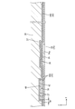
- the top view which shows the plane structure of the display area in the array substrate which comprises a liquid crystal panel
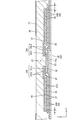
- a plan view showing a planar configuration in the vicinity of the TFT on the array substrate Sectional view along line vii-vii in FIG. Sectional view along the viii-vii line in FIG.
- FIG. 6 The top view which shows the state which patterned the resist apply
- FIG. 10 is an enlarged sectional view taken along line xiii-xii.
- 14 is an enlarged cross-sectional view along the xv-xv line in FIG.
- FIG. 16 is an enlarged cross-sectional view along the line xvii-xvii
- the top view which shows the plane structure of TFT vicinity in the array substrate which concerns on Embodiment 2 of this invention
- FIGS. 1 A first embodiment of the present invention will be described with reference to FIGS.
- a liquid crystal panel (display element) 11 constituting the liquid crystal display device 10 is illustrated.
- a part of each drawing shows an X axis, a Y axis, and a Z axis, and each axis direction is drawn to be a direction shown in each drawing.
- FIG. 1 is used as a reference, and the upper side of the figure is the front side and the lower side of the figure is the back side.
- the television receiver TV includes a liquid crystal display device (display device) 10, front and back cabinets Ca and Cb that are accommodated so as to sandwich the liquid crystal display device 10, a power supply P, A tuner T and a stand S are provided.
- the liquid crystal display device 10 has a horizontally long rectangular shape as a whole, and includes a liquid crystal panel 11 as a display panel and a backlight device (illumination device) 12 as an external light source, as shown in FIGS. Is integrally held by the bezel 13 or the like.
- the backlight device 12 is a so-called direct type in which a light source is disposed directly under the back surface of the liquid crystal panel 11.
- the backlight device 12 includes a chassis 14 opened on the front side (light emission side, liquid crystal panel 11 side), a reflective sheet (reflective member) 15 laid in the chassis 14, and an optical member attached to an opening portion of the chassis 14. 16, a frame 17 for fixing the optical member 16, a plurality of cold cathode tubes (light sources) 18 accommodated in parallel in the chassis 14, and an end portion of the cold cathode tube 18 while shielding light And a lamp holder 19 having light reflectivity.
- the liquid crystal panel 11 is formed by enclosing a liquid crystal layer 22 containing a liquid crystal material, which is a substance whose optical characteristics change with application of an electric field, between a pair of substrates 20 and 21.
- a liquid crystal material which is a substance whose optical characteristics change with application of an electric field.
- the array substrate display element, active matrix substrate
- the front side light emitting side.
- This is a CF substrate (counter display element, counter substrate) 21.
- a pair of front and back polarizing plates 23 are respectively attached to the outer surface sides of both the substrates 20 and 21.
- the array substrate 20 is formed by laminating a plurality of structures (thin films) on a substantially transparent (translucent) glass substrate GS. Specifically, on the inner surface side (the liquid crystal layer 22 side, the surface facing the CF substrate 21) of the glass substrate GS forming the array substrate 20, a switching element having three electrodes 24a to 24c as shown in FIG. A large number of TFTs (Thin Film Transistors) 24 and pixel electrodes 25 are provided side by side. Around the TFT 24 and the pixel electrodes 25, a grid-like gate wiring 26 and source wiring 27 are disposed so as to surround them. Has been.
- the pixel electrode 25 is made of a transparent conductive film such as ITO (Indium Tin Oxide).
- Both the gate wiring 26 and the source wiring 27 are made of a conductive material.
- the source wiring 27 has a two-layer structure in which different metal films 39 and 40 are laminated.
- the lower metal film 39 is made of titanium (Ti)
- the upper metal film is formed.
- 40 is made of aluminum (Al) (see FIG. 7). Since the lower layer metal film 39 contains titanium, the wiring resistance becomes low resistance, and since it is dense and has high mechanical strength, it can exhibit a high function as a barrier metal, thereby obtaining high connection reliability. be able to.
- the upper metal film 40 contains aluminum, the wiring resistance becomes low and the film formation and processing are easy.
- branch lines 26a and 27a extend from the vicinity of the intersecting portions of the gate line 26 and the source line 27 that intersect with each other, and part of these branch lines 26a and 27a.
- a gate electrode 24a and a source electrode 24b constituting the TFT 24 are configured by (the tip end side in the extending direction).
- the drain electrode 24c constituting the TFT 24 is formed on one end side of a drain wiring (pixel connection wiring) 34 described later.
- the array substrate 20 is provided with a capacitor wiring (auxiliary capacitor wiring, storage capacitor wiring, Cs wiring) 33 that is parallel to the gate wiring 26 and overlaps the pixel electrode 25 in a plan view.
- the capacity wiring 33 is alternately arranged with the gate wiring 26 in the Y-axis direction, and the interval between the adjacent gate wiring 26 and the capacity wiring 33 is set to be approximately equal.
- the gate wiring 26 is disposed between the pixel electrodes 25 adjacent to each other in the Y-axis direction, whereas the capacitor wiring 33 is disposed at a position that substantially crosses the central portion of each pixel electrode 25 in the Y-axis direction. Note that the source wiring 27, the gate wiring 26, and the capacitor wiring 33 that intersect with each other are kept in an insulated state by interposing the gate insulating film 35 therebetween.
- the end portion of the array substrate 20 is provided with a terminal portion routed from the gate wiring 26 and the capacitor wiring 33 and a terminal portion routed from the source wiring 27, and each of these terminal portions includes:
- Each signal or reference potential is input from an external circuit (not shown), and the driving of the TFT 24 is thereby controlled.
- An alignment film 28 for aligning liquid crystal molecules contained in the liquid crystal layer 22 is formed on the inner surface side of the array substrate 20.
- the CF substrate 21 is formed by laminating a structure on the plate surface of a glass substrate GS that is substantially transparent (having translucency) like the array substrate 20. Specifically, on the inner surface side (the liquid crystal layer 22 side, the surface facing the array substrate 20) of the glass substrate GS forming the CF substrate 21, as shown in FIG. A large number of color filters are arranged side by side at a position where they are superimposed on each other. In the color filter, the colored portions 29 exhibiting R (red), G (green), and B (blue) are arranged alternately along the X-axis direction. In addition, the outer shape of each colored portion 29 has a vertically long rectangular shape in plan view following the outer shape of the pixel electrode 25.
- each coloring part 29 which comprises a color filter
- the light-shielding part (black matrix) 30 which makes the grid
- the light shielding portion 30 is disposed so as to overlap with the gate wiring 26, the source wiring 27, and the capacitor wiring 33 on the array substrate 20 in plan view.
- a counter electrode 31 is provided on the surface of each colored portion 29 and the light shielding portion 30 so as to face the pixel electrode 25 on the array substrate 20 side.
- An alignment film 32 for aligning liquid crystal molecules contained in the liquid crystal layer 22 is formed on the inner surface side of the CF substrate 21.
- the TFT 24 which is a switching element among the structures of the array substrate 20 will be described in detail.
- the TFT 24 has a structure in which a plurality of thin films are sequentially stacked on the glass substrate GS forming the array substrate 20, and specifically, from the lower layer side (glass substrate GS side).
- a gate electrode 24a connected to the gate wiring 26, a gate insulating film 35, a semiconductor film 36, a doping semiconductor film 42, a source electrode 24b connected to the source wiring 27, a drain electrode 24c connected to the drain wiring 34, and an interlayer An insulating film (passivation film) 37 and a protective film 38 are stacked.
- the pixel electrode 25, the gate insulating film 35, the interlayer insulating film 37, and the protective film 38 are not shown.
- the gate electrode 24a is made of the same material as the gate wiring 26 and is patterned immediately above the glass substrate GS in the same process as the gate wiring 26.
- the gate electrode 24a extends from the vicinity of the intersection of the gate wiring 26 extending along the X-axis direction with the source wiring 27 along the Y-axis direction at the extending tip of the branch line 26a. It consists of parts.
- the gate insulating film 35 is made of, for example, a silicon nitride film (SiNx), and as shown in FIG. 7, the gate electrode 24a and the semiconductor film 36 described below are kept in an insulating state.
- the gate insulating film 35 has a solid pattern that covers not only the TFT 24 formation region but also the entire surface of the glass substrate GS.
- the semiconductor film 36 is made of, for example, amorphous silicon (a-Si). One end side is connected to the source electrode 24b and the other end side is connected to the drain electrode 24c. Have. As shown in FIG. 6, the semiconductor film 36 has a smaller dimension in the Y-axis direction (a direction perpendicular to the arrangement direction of the source electrode 24b and the drain electrode 24c) than the gate electrode 24a. 24b and the drain electrode 24c are larger.
- the doped semiconductor film 42 is made of amorphous silicon (n + Si) doped with an n-type impurity such as phosphorus (P) at a high concentration.
- the doping semiconductor film 42 extends along the semiconductor film 36 but is removed with respect to the range of the channel region CH, and a pair of portions arranged with the channel region CH interposed therebetween are a source electrode 24b and a drain described below. It constitutes a part of the electrode 24c.
- the dimension of the doping semiconductor film 42 in the Y-axis direction is substantially the same as that of the source electrode 24b and the drain electrode 24c.
- the source electrode 24 b and the drain electrode 24 c include the same material as the source wiring 27 and the drain wiring 34 and are patterned on the glass substrate GS in the same process as the source wiring 27 and the drain wiring 34. As shown in FIGS. 6 and 7, the source electrode 24 b and the drain electrode 24 c are arranged to face each other with a predetermined interval in the X-axis direction. The source electrode 24b and the drain electrode 24c are disposed on the upper layer side with respect to the gate electrode 24a via the gate insulating film 35 and the semiconductor film 36, respectively, and a part (opposing portion) of the source electrode 24b and the drain electrode 24c is planar with respect to the gate electrode 24a. The overlapping portion is placed on the gate electrode 24a. As shown in FIG.
- the source electrode 24b and the drain electrode 24c are composed of a first conductive film 24b1, 24c1 on the lower layer side (semiconductor film 36 side) and a second conductive film 24b2, on the upper layer side (interlayer insulating film 37 side). 24c2 is laminated.
- the first conductive films 24b1 and 24c1 on the lower layer side are respectively constituted by the end portions of the doping semiconductor film 42 described above, and function as ohmic contact layers that are in ohmic contact with the semiconductor film 36 on the lower layer side. is there.
- the second conductive films 24b2 and 24c2 on the upper layer side have a two-layer structure in which different metal films are laminated, and the metal film 39 on the lower layer side is made of titanium (Ti), whereas the metal on the upper layer side is made.
- the film 40 is made of aluminum (Al). That is, the source electrode 24b and the drain electrode 24c are common to the source wiring 27 in that they have the second conductive films 24b2 and 24c2 made of two metal films 39 and 40.
- the structure differs from the source wiring 27 in that the first conductive films 24b1 and 24c1 are provided.
- the source wiring 27 includes only the second conductive films 24b2 and 24c2 (39, 40) of the source electrode 24b and the drain electrode 24c, and does not have the first conductive films 24b1 and 24c1 (42). However, these are different in configuration. Further, as shown in FIG. 6, the source electrode 24b extends along the branch line 27a extending along the X-axis direction from the vicinity of the intersection with the gate wiring 26 in the source wiring 27 extending along the Y-axis direction. It is comprised by the protrusion front-end
- the source electrode 24b and the drain electrode 24c are arranged to face each other with a predetermined interval therebetween, and thus are not directly electrically connected to each other.
- the source electrode 24b and the drain electrode 24c are indirectly electrically connected via the semiconductor film 36 on the lower layer side, and the bridge portion between the electrodes 24b and 24c in the semiconductor film 36 has a drain current. It functions as a flowing channel region CH.
- the source electrode 24b and the drain electrode 24c are symmetrical with each other.
- the interlayer insulating film 37 is made of, for example, a silicon nitride film (SiNx), and is made of the same material as the gate insulating film 35 described above.
- the protective film 38 is made of an acrylic resin (for example, polymethyl methacrylate resin (PMMA)) or a polyimide resin, which is an organic material. Therefore, the protective film 38 is thicker than the gate insulating film 35 and the interlayer insulating film 37 made of other inorganic materials and functions as a planarizing film. Both the interlayer insulating film 37 and the protective film 38 have a solid pattern extending over almost the entire surface of the glass substrate GS as well as the region where the TFT 24 is formed.
- the interlayer insulating film 37 and the protective film 38 are disposed between the source wiring 27, the drain wiring 34, and the contact portion 41 on the relatively lower layer side and the pixel electrode 25 on the relatively upper layer side outside the region where the TFT 24 is formed. It is assumed that they are interposed and kept in an insulated state.
- the drain wiring 34 connected to the drain electrode 24c is substantially L-shaped in plan view as shown in FIG. 6, and one end side of the drain wiring 34 is connected to the drain electrode 24c. The other end is connected to a contact portion 41 that is in contact with the pixel electrode 25.
- the drain wiring 34 extends from the drain electrode 24c along the X-axis direction, is then bent toward the capacitor wiring 33 side, and extends along the Y-axis direction, thereby connecting to the contact portion 41.
- the drain wiring 34 is formed on the gate insulating film 35, is made of the same material as the source wiring 27, and has the same two-layer structure.
- the drain wiring 34 is composed of only the second conductive films 24b2 and 24c2 (39, 40) of the source electrode 24b and the drain electrode 24c, as in the case of the source wiring 27, and the first conductive films 24b1, 24c1 (42). It differs from these in that it does not have.
- the contact portion 41 is arranged at a position that overlaps the capacitive wiring 33 that is a light shielding region in a plan view. Accordingly, as the structure for contacting the pixel electrode 25 with the contact portion 41 is formed, irregularities are formed on the surfaces of the pixel electrode 25 and the alignment film 28, which causes the alignment of the liquid crystal molecules contained in the liquid crystal layer 22. Even when the state is disturbed, the occurrence of light leakage can be avoided.
- the contact portion 41 has a horizontally long rectangular shape along the extending direction (X-axis direction) of the capacitor wiring 33 when viewed in plan, and the short side dimension is narrower than the wiring width of the capacitor wiring 33.
- the contact portion 41 is connected to the other end of the drain wiring 34, that is, the end opposite to the drain electrode 24c side, and the left side (shown in FIG. 6) along the X-axis direction from the end of the drain wiring 34. It is arranged so as to protrude to the TFT 24 side.
- the contact portion 41 is made of the same material as the source wiring 27 and the drain wiring 34 described above, and is patterned on the glass substrate GS in the same process as the source wiring 27 and the drain wiring 34.
- the contact portion 41 is formed on the gate insulating film 35, and an interlayer insulating film 37, a protective film 38, and the pixel electrode 25 are stacked in that order on the upper layer side. In the interlayer insulating film 37 and the protective film 38, a contact hole 43 is formed at a position overlapping the contact portion 41 in plan view, and the pixel electrode 25 is connected to the contact portion 41 through the contact hole 43. Connected.
- the semiconductor film 36 and the doping semiconductor film 42 are viewed in plan with respect to the source wiring 27 and the drain wiring 34 as shown in FIG.
- semiconductor film extending portions 44 extending to the overlapping range are formed.
- the semiconductor film extending portion 44 is formed by extending the semiconductor film 36 and the doping semiconductor film 42 and is made of the same material as that of the semiconductor film 36 and the doping semiconductor film 42 and is patterned in the same process.
- the semiconductor film extending portion 44 has a two-layer structure including an extended portion of the lower semiconductor film 36 and an extended portion of the upper doped semiconductor film 42.
- the semiconductor film extending portion 44 is connected to the source wiring 27 from both ends of the semiconductor film 36 and the doping semiconductor film 42 opposite to the channel region CH side in the X-axis direction (alignment direction of the source electrode 24b and the drain electrode 24c). A pair is formed so as to extend along the drain wiring 34.
- the semiconductor film extending portion 44 has the same dimension in the Y-axis direction in the portion extending along the X-axis direction from the end portions of the semiconductor film 36 and the doping semiconductor film 42, and the same dimension of the semiconductor film 36 in the formation region of the TFT 24. It is relatively small.
- first semiconductor film extending portion what is superimposed on the source wiring 27 is referred to as a “first semiconductor film extending portion”, and a suffix A is added to the drain wiring 34.
- second semiconductor film extending portion the superimposing part is added as a “second semiconductor film extending portion” with a subscript B, and when referring generically without distinction, the subscript is not added.
- the first semiconductor film extending portion 44A includes, as shown in FIGS. 6 and 7, the semiconductor film 36 and the doping semiconductor film 42 and the end portion of the source electrode 24b. Is further extended along the branch line 27a (X-axis direction) of the source wiring 27 toward the left side (the main body side of the source wiring 27) shown in FIGS. 6 and 7, thereby lower layer side with respect to the branch line 27a. It is arranged to overlap. Since the first semiconductor film extending portion 44A is constituted by extending portions of the semiconductor film 36 and the doping semiconductor film 42, the branch line 27a of the source wiring 27 stacked thereon is connected to the source electrode 24b. In this way, the connection is made in a flat state without any step.
- the first semiconductor film extending portion 44A When the first semiconductor film extending portion 44A reaches the main body of the source wiring 27 (the trunk line excluding the branch line 27a), it further extends vertically along the main body of the source wiring 27 in the Y-axis direction as shown in FIG. As a result, the main body of the source wiring 27 is arranged so as to overlap with the lower layer side.
- the first semiconductor film extending portion 44 ⁇ / b> A is formed over a range that overlaps the substantially entire area of the main body of the source wiring 27 in a plan view. That is, the first semiconductor film extending portion 44A is formed over a range that overlaps almost the entire area of the source wiring 27 including the branch line 27a in a plan view.
- the first semiconductor film extending portion 44A is present over almost the entire area on the lower layer side of the main body of the source wiring 27, whereby the source wiring 27 is located over the entire area than the first semiconductor film extending portion 44A. There is no contact with the gate insulating film 35 on the lower layer side, and no step is caused.
- the first semiconductor film extension 44 ⁇ / b> A is formed over a wider area than the overlapping source wiring 27 (including the branch line 27 a) in a plan view.
- the size (area) is relatively large.
- the extended portion of the lower semiconductor film 36 in the first semiconductor film extending portion 44 ⁇ / b> A has both outer edges extending substantially along the extending direction as shown in FIGS. 6 to 9. 27 is arranged outside the both outer edges.
- the extended portion of the semiconductor film 36 on the lower layer side of the first semiconductor film extending portion 44A has the center position in the width direction substantially coincided with the center position in the width direction of the source wiring 27, and each outer edge and the source wiring
- the distance (width of non-overlapping portion) D1 between the 27 corresponding outer edges is substantially equal (see FIGS. 7 and 9).
- the extended portion of the upper doped semiconductor film 42 in the first semiconductor film extending portion 44A has substantially the same line width as the source wiring 27 and may protrude from both outer edges when seen in a plan view. Not supposed to be.
- the second semiconductor film extending portion 44B of the pair of semiconductor film extending portions 44 is formed by further separating the semiconductor film 36 and the doping semiconductor film 42 from the end of the drain electrode 24c. It is formed so as to extend in parallel with the wiring 34, and has a bent shape that is substantially L-shaped in a plan view as in the case of the drain wiring 34. Thereby, the second semiconductor film extension 44 ⁇ / b> B is disposed so as to overlap the lower layer side of the drain wiring 34. Since the second semiconductor film extending portion 44B is constituted by extending portions of the semiconductor film 36 and the doping semiconductor film 42, the drain wiring 27 stacked thereon has a step in the middle of the drain electrode 24c.
- the second semiconductor film extension 44 ⁇ / b> B is formed over a range that overlaps almost the entire area of the drain wiring 34 in a plan view. Further, the second semiconductor film extending portion 44B is configured to extend to a range overlapping with the contact portion 41 connected to the end portion of the drain wiring 34 when viewed in a plane. Specifically, the end of the second semiconductor film extending portion 44B opposite to the drain electrode 24c side protrudes toward the left side shown in FIG. The second semiconductor film extending portion 44 ⁇ / b> B is formed over a range that overlaps substantially the entire region of the contact portion 41 in a plan view.
- the second semiconductor film extending portion 44B is present over almost the entire region on the lower layer side of the drain wiring 34 and the contact portion 41, whereby the drain wiring 34 and the contact portion 41 are disposed over the entire region of the second semiconductor film. There is no contact with the gate insulating film 35 on the lower layer side than the extending portion 44B, and no step is caused accordingly.
- the second semiconductor film extension 44 ⁇ / b> B is formed over a wider area in a plan view than the overlapping drain wiring 34 and the contact part 41, and has a size (see in a plan view). Area) is relatively larger than these.
- the overlapping portion with the drain wiring 34 has both outer edges along the extending direction as shown in FIG. Is disposed outside the outer edges of the drain wiring 34.
- the outer peripheral edge of the overlapping portion with the contact portion 41 is arranged outside the outer peripheral edge of the contact portion 41.
- the extended portion of the semiconductor film 36 on the lower layer side in the second semiconductor film extending portion 44B has its outer peripheral edge disposed almost outside the both outer edges of the drain wiring 34 and the outer peripheral edge of the contact portion 41. .
- the overlapping portion with the drain wiring 34 is substantially coincident with the central position in the width direction of the drain wiring 34.
- the distances (widths of non-overlapping portions) D1 between the outer edges and the corresponding outer edges of the drain wiring 34 are substantially equal.
- This distance D1 is equal to the distance D1 between each outer edge of the extended portion of the semiconductor film 36 on the lower layer side in the first semiconductor film extending portion 44A described above and each corresponding outer edge of the source wiring 27. (See FIGS. 6, 7 and 9).
- the overlapping portion with the contact portion 41 has a center position substantially coincident with the center position of the contact portion 41, The distance from the outer peripheral edge of the contact portion 41 (the width of the non-overlapping portion) is substantially equal over the entire circumference.
- This distance is the distance D1 between each outer edge of the extended portion of the semiconductor film 36 on the lower layer side in the first semiconductor film extension 44A described above and each corresponding outer edge of the source wiring 27, and the second semiconductor film extension.
- the distance D1 between each outer edge of the overlapping portion of the existing portion 44B with the drain wiring 34 and each corresponding outer edge of the drain wiring 34 is set (see FIG. 6). That is, the semiconductor film extension 44 according to the present embodiment has a distance (non-overlapping) between the outer periphery and the outer periphery of the structure (source wiring 27, drain wiring 34, and contact part 41) to be superimposed.
- the width (D1) of the portion is substantially the same over the entire area.
- the extension portion of the upper semiconductor layer 42 in the second semiconductor film extension portion 44B has substantially the same size as the drain wiring 27 and the contact portion 41 in plan view, and is seen in plan view.
- the drain wiring 27 and the contact portion 41 do not protrude from the outer edges.
- This embodiment has the structure as described above, and its operation will be described next.
- the manufacturing procedure of the array substrate 20 in the liquid crystal panel 11 will be described in detail.
- Each structure is sequentially stacked on the plate surface of the glass substrate GS forming the array substrate 20 by a known photolithography method. Specifically, first, the gate electrode 24a, the gate wiring 26, and the capacitor wiring 33 as the first layer are patterned on the surface of the glass substrate GS using a predetermined photomask, and then the gate insulation as the second layer. A film 35 is formed, and the semiconductor film 36 as the third layer and the doping semiconductor film 42 as the fourth layer are patterned using a predetermined photomask. At this time, the semiconductor film extending portion 44 constituted by the extended portions of the semiconductor film 36 and the doping semiconductor film 42 is extended to the formation planned range of the source wiring 27, the drain wiring 34, and the contact portion 41. .
- the source electrode 24b and the drain electrode 24c are composed of a fourth layer (doping semiconductor film 42) and a fifth layer (metal films 39 and 40).
- a semiconductor material film made of the material of the semiconductor film 36 and a doping semiconductor material film made of the material of the doping semiconductor film 42 are sequentially formed on the glass substrate GS patterned with the second layer, and the upper layer side A resist is further applied on the solid doped semiconductor material film. After the applied resist is exposed through a predetermined photomask and the resist is developed, the semiconductor material film and the doped semiconductor material film are subsequently etched (for example, dry etching), whereby the semiconductor film 36 having a predetermined pattern is obtained. Then, the doping semiconductor film 42 and the semiconductor film extending portion 44 are formed.
- an extended portion of the doping semiconductor film 42 constituting the doping semiconductor film 42 and the semiconductor film extending portion 44 is an extended portion of the semiconductor film 36 and the semiconductor film 36 constituting the semiconductor film extending portion 44 in a plan view. And the same pattern shape (same size in plan view).
- the upper layer metal material film M2 made of aluminum which is the material of the side metal film 40 is formed, a resist R is applied on the solid upper layer metal material film M2.
- the applied resist R is exposed to light through a predetermined photomask and then developed, so that the pattern shown in FIG. 10 is obtained.
- the remaining formation range of the resist R coincides with the planned formation range of the source electrode 24b, the drain electrode 24c, the source wiring 27, the drain wiring 34, and the contact portion 41.
- the shaded range is the formation range of the patterned resist R.
- the solid gate insulating film 35, the lower metal material film M1, and the upper metal material film M2 are not shown.
- the metal material films M1 and M2 are etched using the resist R as a mask.
- an etching solution is supplied to the glass substrate GS to etch portions of the metal material films M1 and M2 that are not covered with the resist R. Remove by corrosive dissolution with liquid.
- the etching range in each of the metal material films M1 and M2 is theoretically coincident with an uncovered region that is not covered with the resist R.
- the resist Even if it is a covered region by R, there is a possibility that the etching solution that has penetrated into the adjacent non-covered region penetrates beyond the boundary and is over-etched.
- substrate in each metal material film M1, M2 can change with the presence or absence of a level
- the thickness of the semiconductor film and the doping semiconductor film is added to each metal material film stacked thereon. Since a step with the combined height is generated, the adhesion between the metal material films and the adhesion between the lower metal material film and the gate insulating film may be significantly deteriorated at the step. As a result, over-etching with an etching solution is likely to occur, and the line width becomes narrower than planned or disconnection is likely to occur. In this regard, in the present embodiment, as shown in FIGS.
- each of the metal material films M1 and M2 is disposed on the semiconductor film 36, the doping semiconductor film 42, and the semiconductor film extending portion 44 that is an extension thereof over almost the entire area.
- the metal material films M1 and M2 do not have a level difference caused by the semiconductor film 36 and the doping semiconductor film 42 as in the prior art, and thereby have relatively good adhesion to the base. It has become.
- each of the metal material films M1 and M2 can be accurately etched according to the pattern of the resist R, the boundary position between the source electrode 24b and the source wiring 27 formed by the etching, the drain electrode 24c and the drain wiring 34. It is possible to effectively prevent the line width from being narrowed or disconnection from occurring at the boundary position. Thereby, high connection reliability can be obtained, and the operational reliability of the TFT 24 and the reliability related to the display of the liquid crystal display device 10 can both be improved.
- a disconnection occurs in the middle of the source wiring 27, it can be remedied by a wiring repair means such as a spare wiring (not shown), whereas the boundary position between the source electrode 24b and the source wiring 27
- a wiring repair means such as a spare wiring (not shown)
- the boundary position between the source electrode 24b and the source wiring 27 there is a circumstance that such relief is extremely difficult.
- the semiconductor film extending portion 44 since the semiconductor film extending portion 44 according to the present embodiment extends to a range overlapping in plan view over almost the entire area of the source wiring 27, the drain wiring 34, and the contact portion 41, the source wiring 27. The occurrence of disconnection or the like can be prevented in almost the entire region of the drain wiring 34 and the contact portion 41, and the connection reliability can be further improved.
- each metal material film M1, M2 there are cases where dry etching and wet etching are performed before and after the time. In this case, only the upper metal material film M2 is selectively etched by wet etching. Even in such a case, the same effect as described above, that is, the effect of preventing disconnection of the upper metal material film M2 can be obtained.
- the doping semiconductor film 42 (including the extended portion of the doping semiconductor film 42 in the semiconductor film extending portion 44) is continuously etched, and then the upper layer side metal material The resist R on the film M2 is peeled off. Thereby, the doping semiconductor film 42 can be separated into the left and right sides with an interval corresponding to the channel region CH of the semiconductor film 36.
- the interlayer insulating film 37 as the sixth layer and the protective film 38 as the seventh layer are successively formed. These are formed into a film and patterned in a lump.
- the alignment film 28 is further formed thereon, whereby the manufacture of the array substrate 20 is completed.
- the manufactured array substrate 20 is bonded to a separately manufactured CF substrate 21 with the liquid crystal layer 22 interposed therebetween, whereby the liquid crystal panel 11 shown in FIG. 4 is obtained.
- the manufactured liquid crystal panel 11 is assembled to the backlight device 12 via the bezel 13, whereby the liquid crystal display device 10 shown in FIGS. 2 and 3 is obtained.
- a third layer (semiconductor film 36) and a fourth layer (doping semiconductor film 42), and a fifth layer (source wiring 27, drain) are formed. Since the wiring 34 and the contact portion 41) are patterned by using different photomasks, depending on the exposure accuracy, the position is shifted from the normal position (designed position) in the direction along the plate surface of the array substrate 20. May be formed. However, in the present embodiment, the extended portions of the semiconductor film 36 in the semiconductor film 36 and the semiconductor film extending portion 44 are viewed in a plane more than the source electrode 24b, the drain electrode 24c, the source wiring 27, the drain wiring 34, and the contact portion 41.
- the difference in size (distance D1, margin) in a plan view between the extended portion of the semiconductor film 36 in the semiconductor film extending portion 44 and the source wiring 27, the drain wiring 34, and the contact portion 41 is determined in the manufacturing apparatus.
- a relatively small source wiring 27, drain wiring 34, and contact portion 41 with respect to the extended portion of the semiconductor film 36 in the relatively large semiconductor film extending portion 44 Even when the position is displaced in the Y-axis direction, the amount of displacement is not designed to exceed the distance D1, so that the source wiring 27, the drain wiring 34, and the contact portion 41 include the semiconductor film extending portion 44.
- the semiconductor film 36 is located on the inner side of the outer edges of the extended portion of the semiconductor film 36, and the situation of protruding outward from either of the outer edges is reliably avoided. Further, as shown in FIGS.
- the relatively small source wiring 27, drain wiring 34, and contact portion 41 with respect to the extended portion of the semiconductor film 36 in the relatively large semiconductor film extending portion 44 are connected to the X axis. Even when the position is displaced in the direction, since the amount of displacement is not designed to exceed the distance D1, the source wiring 27, the drain wiring 34, and the contact portion 41 are formed in the semiconductor film extending portion 44. It exists in the inner side rather than the both outer edges of the extension part of 36, and the situation which protrudes outside from either of both outer edges is avoided reliably. Accordingly, the extension of the semiconductor film 36 in the semiconductor film extension 44 and the overall size of the source wiring 27, drain wiring 34, and contact part 41 are relatively wide in size.
- the extended portion of the semiconductor film 36 at 44 is dominant, and even if the source wiring 27, the drain wiring 34, and the contact portion 41 are displaced, they hardly change and are always kept constant. As a result, the extended portion of the semiconductor film 36 in the semiconductor film extending portion 44, both of which are conductors, and the source wiring 27, the drain wiring 34, and the contact portion 41 are formed between other wirings such as the capacitor wiring 33, for example. It is avoided that the capacitance value to be changed fluctuates. If the capacitance value formed between the capacitor wiring 33 and the capacitor wiring 33 is stabilized, it is possible to avoid fluctuations in the voltage value charged in the pixel electrode 25 forming a capacitor with the capacitor wiring 33. Accordingly, it is possible to avoid variation in the gradation value of the display image displayed based on the voltage value charged in the pixel electrode 25 and to obtain a good display quality.
- the array substrate (display element) 20 of the present embodiment includes the glass substrate (substrate) GS, the gate wiring 26 formed on the glass substrate GS, and the gate electrode 24a formed on the gate wiring 26.
- Drain electrode 24c formed in the semiconductor film 36 and extending to at least a portion overlapping the source wiring 27 in plan view. And a Makunobezai portion 44.
- the source electrode 24b and the drain electrode 24c are provided between them.
- a drain current flows through the channel region CH of the semiconductor film 36.
- the semiconductor film extending portion 44 is formed on the semiconductor film 36 so as to extend to a range overlapping at least a part of the source wiring 27 in plan view, the source electrode 24b and the source wiring 27 are formed. It is possible to avoid a step due to the semiconductor film 36 between the two.
- connection reliability can be improved.
- the semiconductor film extending portion 44 extends to a range overlapping with almost the entire area of the source wiring 27 in a plan view. By doing so, it is possible to prevent disconnection or the like caused by the semiconductor film 36 in almost the entire area of the source wiring 27, and therefore connection reliability can be further improved.
- the semiconductor film extending portion 44 is formed so as to be larger than the source wiring 27 in a plan view. Even if the semiconductor film extending portion 44 and the source wiring 27 are displaced in one direction along the planar direction due to the influence of an accuracy error or the like that may occur in manufacturing, the semiconductor film extending portion 44 is not connected to the source wiring. 27 when viewed from the plane, so that when the amount of positional deviation is within the range of the difference in size in one direction, the semiconductor film extension 44 and the source wiring 27 are viewed from the plane. Variations in the overall size can be avoided. This makes it difficult for the semiconductor film extension 44 and the source wiring 27 to change in the value of the capacitance formed with other wirings, thereby avoiding a situation in which electrical adverse effects are caused.
- the semiconductor film extension 44 and the source wiring 27 can change in the value of the capacitance formed with other wirings, thereby avoiding a situation in which electrical adverse effects are caused.
- the semiconductor film extending portion 44 has both outer edges arranged outside the both outer edges of the source wiring 27. In this way, even when the semiconductor film extending portion 44 and the source wiring 27 are displaced in one direction along the plane direction, the situation where the source wiring 27 protrudes from either of the outer edges of the semiconductor film 36 occurs. Can be prevented.
- the source electrode 24b and the drain electrode 24c are each a stacked structure of a doping semiconductor film 42 formed on the semiconductor film 36 to which impurities are added and metal films 39 and 40 formed on the doping semiconductor film 42 and made of a metal material.
- the source wiring 27 is made of the same material as the metal films 39 and 40 constituting the source electrode 24b, and the semiconductor film extending portion 44 is an end of the doping semiconductor film 42. From the portion to the source wiring 27 side. In this way, the metal films 39 and 40 forming the source electrode 24 b and the drain electrode 24 c are in ohmic contact with the semiconductor film 36 by the doping semiconductor film 42.
- the semiconductor film extension 44 extends from the end of the doping semiconductor film 42 to the source wiring 27 side, the ends of the doping semiconductor film and the semiconductor film are aligned as in the conventional case.
- the step formed is a film of the doping semiconductor film 42. Only the thickness is sufficient. Thereby, disconnection etc. can be made hard to occur and high connection reliability can be obtained.
- the drain electrode 34 formed on the pixel electrode 25 and the gate insulating film 35 and having one end connected to the drain electrode 24 c and the other end of the drain interconnect 34 and connected to the pixel electrode 25.
- the semiconductor film extending portion 44 extends to a range that overlaps at least a part of the drain wiring 34 in a plan view. In this way, based on the scanning signal and the data signal supplied to the gate wiring 26 and the source wiring 27, respectively, the pixel electrode 25 is connected to the pixel electrode 25 through the drain wiring 34 and the contact portion 41 connected to the drain electrode 24c. The voltage can be charged.
- the semiconductor film extending portion 44 extends to a range that overlaps at least a portion of the drain wiring 34 in a plan view, the semiconductor film 36 is formed between the drain electrode 24 c and the drain wiring 34. It is possible to avoid the resulting level difference. As a result, disconnection or the like hardly occurs when wet etching is performed on the drain electrode 24c and the drain wiring 34 in the manufacturing process, and thus high connection reliability can be obtained.
- the semiconductor film extending portion 44 extends to a range that overlaps with almost the entire area of the drain wiring 34 in a plan view. In this way, it is possible to prevent disconnection or the like due to the semiconductor film 36 in almost the entire region of the drain wiring 34, and to further improve connection reliability.
- the semiconductor film extending portion 44 is formed to be larger than the drain wiring 34 in a plan view. Even if the semiconductor film extension 44 and the drain wiring 34 are misaligned in one direction along the plane direction due to the influence of an accuracy error that may occur in the manufacturing process, the semiconductor film extension 44 is not connected to the drain wiring. When the amount of positional deviation is within the range of the difference in size in one direction, the semiconductor film extension 44 and the drain wiring 34 are viewed in a plane. Variations in the overall size can be avoided. This makes it difficult for the semiconductor film extension 44 and the drain wiring 34 to change in the value of the capacitance formed between the semiconductor wiring extension 44 and the drain wiring 34 and the like, thereby avoiding a situation where an electrical adverse effect is caused.
- the semiconductor film extension 44 and the drain wiring 34 can change in the value of the capacitance formed between the semiconductor wiring extension 44 and the drain wiring 34 and the like, thereby avoiding a situation where an electrical adverse effect is caused.
- the semiconductor film extending portion 44 has both outer edges arranged outside the both outer edges of the drain wiring 34. In this way, even when the semiconductor film extending portion 44 and the drain wiring 34 are displaced in one direction along the plane direction, the situation where the drain wiring 34 protrudes from either of the outer edges of the semiconductor film 36 occurs. Can be prevented.
- the semiconductor film extending portion 44 extends to a range overlapping with almost the entire area of the contact portion 41 in a plan view. In this way, it is possible to prevent disconnection or the like due to the semiconductor film 36 in almost the entire contact portion 41 in addition to the drain wiring 34, and the connection reliability can be further improved.
- the semiconductor film extending portion 44 is formed larger than the contact portion 41 in a plan view. Even if the semiconductor film extending portion 44 and the contact portion 41 are misaligned in one direction along the plane direction due to the influence of an accuracy error that may occur in manufacturing, the semiconductor film extending portion 44 is in contact with the contact portion. 41 is larger than 41 in a plan view, and if the amount of positional deviation is within the range of the difference in size in one direction, the semiconductor film extension 44 and the contact portion 41 are viewed in a plane. Variations in the overall size can be avoided. As a result, the semiconductor film extending portion 44 and the contact portion 41 are less likely to change in the value of the capacitance formed between other wirings and the like, thereby avoiding a situation where an electrical adverse effect is caused.
- the semiconductor film extending portion 44 and the contact portion 41 are less likely to change in the value of the capacitance formed between other wirings and the like, thereby avoiding a situation where an electrical adverse effect is caused.
- the outer peripheral edge of the semiconductor film extending portion 44 is arranged outside the outer peripheral edge of the contact portion 41. In this case, even when the semiconductor film extending portion 44 and the contact portion 41 are displaced in one direction along the plane direction, the contact portion 41 protrudes from any one of the outer peripheral edges of the semiconductor film 36. Can be prevented.
- the semiconductor film extending portion 144 is configured to extend to a range overlapping each part of the source wiring 27 and the drain wiring 34 in a plan view. ing. Specifically, the first semiconductor film extension portion 144A extends along the X-axis direction from the end portion on the source electrode 24b side in the semiconductor film 136 and the doping semiconductor film (not shown) toward the main body of the source wiring 27. At the same time, it overlaps the entire area of the branch line 27a in the source wiring 27 and the connection portion of the branch line 27a in the main body in a plan view.
- the first semiconductor film extending portion 144A is in a relationship that does not overlap in plan view with respect to most of the main body of the source wiring 27 except for the connection portion of the branch line 27a.
- the second semiconductor film extending portion 144B extends along the X-axis direction along the drain wiring 34 from the end on the drain electrode 24c side in the semiconductor film 136 and the doping semiconductor film. 34, the first portion 34a along the X-axis direction overlaps substantially the entire region in a plan view. Accordingly, the second semiconductor film extending portion 144B is in a relationship that does not overlap in a plan view with respect to almost the entire area of the second portion 34b along the Y-axis direction in the drain wiring 34.
- the second semiconductor film extending portion 144B avoids the occurrence of a step due to the semiconductor film 136 and the doping semiconductor film. It is possible to effectively prevent the width from narrowing or disconnection.
- the first semiconductor film extending portion extends over a range that overlaps a part of the source wiring in plan view.
- the general formation range can be changed as appropriate.
- the first semiconductor film extension is formed so as to overlap in plan view with the whole area of the branch line of the source wiring and a predetermined length portion including the connection part of the branch line in the main body of the source wiring. It can be a range.
- the first semiconductor film extending portion may be formed so as to overlap with only a part of the branch line of the source wiring in a plan view and not to overlap with the main body of the source wiring in a plan view.
- the second semiconductor film extending portion extends over a range overlapping in plan view with respect to a part of the drain wiring.
- the general formation range can be changed as appropriate.
- the extended portion of the second semiconductor film overlaps the entire area of the drain wiring in a plan view, but can be a formation range that does not overlap the contact portion in a plan view.
- the second semiconductor film extending portion may be a formation range that overlaps the entire area of the first portion of the drain wiring and a part of the second portion in plan view.
- the second semiconductor film extending portion is overlapped in plan view only on a part of the first portion of the drain wiring, and is not overlapped in plan view with the second portion of the drain wiring and the remaining portion of the first portion. It can also be a range.
- the second semiconductor film extending portion may be a formation range that overlaps the entire area of the drain wiring and a part of the contact portion in plan view.
- the semiconductor film extension portion and the source wiring, the drain wiring, and the contact portion are arranged so as to be substantially concentric at the normal position (designed position). It is also possible to adopt a configuration in which is eccentrically arranged.
- one outer edge of the first semiconductor film extending portion is arranged so as to be flush with one outer edge of the source wiring, or the second semiconductor film extending. It is also possible to arrange such that one outer edge in the portion is flush with one outer edge of the drain wiring and one outer edge of the contact portion.
- the first semiconductor film extension portion is shown to have a size over a wide range as viewed in plan than the source wiring.
- the semiconductor film extension portion is the source wiring Those formed in the same size in a plan view are also included in the present invention. This relationship can be similarly applied to the second semiconductor film extending portion, the drain wiring, and the contact portion.
- the outer edge of the semiconductor film extending portion is configured to be arranged outside the outer edges of the source wiring, the drain wiring, and the contact portion. It is also possible to adopt a configuration in which the outer edge is arranged inside the outer edge of at least one of the source wiring, the drain wiring, and the contact portion.
- the drain wiring that connects the contact portion and the drain electrode is exemplified.
- the drain wiring can be omitted as a configuration in which the contact portion is provided on the drain electrode. .
- the present invention can be applied even in such a configuration.
- the second semiconductor film extending portion can be removed. Even in such a case, by providing the first semiconductor film extending portion that overlaps the source wiring in plan view, an effect of preventing disconnection that may occur in the source wiring can be obtained.
- the metal film on the upper layer side constituting the source wiring, drain wiring, contact portion and the like is made of aluminum.
- aluminum for example, molybdenum (Mo) or copper ( Cu) or the like can also be used.
- the metal film on the lower layer side constituting the source wiring, drain wiring, contact portion and the like has been shown to contain titanium, but other than titanium, for example, chromium (Cr), tantalum ( It is also possible to use Ta), copper (Cu), or the like.
- the direct type is exemplified as the backlight device included in the liquid crystal display device, but the present invention includes a backlight device of an edge light type.
- a transmissive liquid crystal display device including a backlight device that is an external light source is exemplified.
- the present invention is applied to a reflective liquid crystal display device that performs display using external light.
- the backlight device can be omitted.
- a TFT is used as a switching element of a liquid crystal display device.
- the present invention can also be applied to a liquid crystal display device using a switching element other than TFT (for example, a thin film diode (TFD)).
- a switching element other than TFT for example, a thin film diode (TFD)
- the present invention can also be applied to a liquid crystal display device for monochrome display.
- the liquid crystal display device using a liquid crystal panel as the display panel has been exemplified.
- the present invention is applicable to a display device using another type of display panel (PDP, organic EL panel, etc.). Applicable. In that case, the backlight device can be omitted.
- SYMBOLS 10 Liquid crystal display device (display device), 12 ... Backlight device (illumination device), 20 ... Array substrate (display element), 21 ... CF substrate (counter display element), 24a ... Gate electrode, 24b ... Source electrode, 24c DESCRIPTION OF SYMBOLS ... Drain electrode, 25 ... Pixel electrode, 26 ... Gate wiring, 27 ... Source wiring, 34 ... Drain wiring, 35 ... Gate insulating film, 36 ... Semiconductor film, 39 ... Lower layer side metal film (metal film), 40 ... Upper layer Side metal film (metal film), 41 ... contact part, 42 ... doping semiconductor film, 44,144 ... semiconductor film extension part, CH ... channel region, GS ... glass substrate (substrate), TV ... TV receiver
Landscapes
- Physics & Mathematics (AREA)
- Nonlinear Science (AREA)
- Engineering & Computer Science (AREA)
- Microelectronics & Electronic Packaging (AREA)
- Mathematical Physics (AREA)
- Chemical & Material Sciences (AREA)
- Crystallography & Structural Chemistry (AREA)
- General Physics & Mathematics (AREA)
- Optics & Photonics (AREA)
- Thin Film Transistor (AREA)
- Liquid Crystal (AREA)
Abstract
An array substrate (20) is provided with: a glass substrate (GS); gate wiring (26) formed on the glass substrate (GS); a gate electrode (24a) formed on the gate wiring (26); a gate insulating film (35) formed on the gate wiring (26) and the gate electrode (24a); a semiconductor film (36), which is formed on the gate insulating film (35), and has a channel region (CH); source wiring (27), which is formed on the gate insulating film (35), and intersects the gate wiring (26); a source electrode (24b), which is formed on the source wiring (27), and is connected to one end side of the semiconductor film (36); a drain electrode (24c), which is connected to the other end side of the semiconductor film (36), and is connected to the source electrode (24b) with the channel region (CH) therebetween; and a semiconductor film extending section (44), which is formed to the semiconductor film (36), and extends to as far as a region that overlaps at least a part of the source wiring (27) in planar view.
Description
本発明は、表示素子、表示装置、及びテレビ受信装置に関する。
The present invention relates to a display element, a display device, and a television receiver.
液晶表示装置に用いられる液晶パネルは、一対のガラス基板間に液晶層が挟持された構成とされているが、そのうち一方のガラス基板は、各画素の動作を制御するためのアクティブ素子としてTFTが形成されたアレイ基板とされる。このアレイ基板には、その表示領域内にゲート配線とソース配線とが多数本ずつ格子状に設けられ、ゲート配線とソース配線との交差部にTFTが設けられた構成を有している。そして、ゲート配線とソース配線とに囲まれた領域に画素電極が配され、これにより表示単位としての画素が構成されている。この種の液晶パネルの一例として下記特許文献1に記載されたものが知られている。
A liquid crystal panel used for a liquid crystal display device has a structure in which a liquid crystal layer is sandwiched between a pair of glass substrates. One of the glass substrates has a TFT as an active element for controlling the operation of each pixel. The formed array substrate is used. This array substrate has a structure in which a large number of gate lines and source lines are provided in a lattice shape in the display region, and TFTs are provided at intersections of the gate lines and the source lines. In addition, a pixel electrode is disposed in a region surrounded by the gate wiring and the source wiring, thereby constituting a pixel as a display unit. As an example of this type of liquid crystal panel, one described in Patent Document 1 below is known.
(発明が解決しようとする課題)
ところで、TFTは、ガラス基板上に形成されゲート配線に接続されたゲート電極と、ゲート電極上に形成されたゲート絶縁膜と、ゲート絶縁膜上に形成されるとともにソース配線に接続されたソース電極と、ゲート絶縁膜上に形成されるとともにコンタクトホールを介して画素電極に接続されたドレイン電極と、一端側がソース電極に他端側がドレイン電極にそれぞれ接続されることでチャネル領域を有する半導体膜とを備えてなる。 (Problems to be solved by the invention)
By the way, the TFT is formed on the glass substrate and connected to the gate wiring, the gate insulating film formed on the gate electrode, and the source electrode formed on the gate insulating film and connected to the source wiring. A drain electrode formed on the gate insulating film and connected to the pixel electrode through the contact hole, and a semiconductor film having a channel region by connecting one end side to the source electrode and the other end side to the drain electrode, It is equipped with.
このうち半導体膜は、ソース電極とドレイン電極とを架け渡す範囲に形成されるものであるのに対し、ソース配線から分岐されたソース電極は、半導体膜の端部に乗り上げるために段差部を有している。この段差部では、当該TFTをフォトリソグラフィ法により形成するに際して、ソース電極及びソース配線をウェットエッチングによりパターニングする工程において、エッチング液が染み込み易くなるおそれがある。その理由は、例えばソース電極と下地であるゲート絶縁膜との密着性が段差部において局所的に悪化するため、などと推考される。エッチング液が段差部に染み込むと、そこで線幅が細くなったり、断線する可能性があり、そうなると接続信頼性を損なうおそれがある。
Among these, the semiconductor film is formed in a range where the source electrode and the drain electrode are bridged, whereas the source electrode branched from the source wiring has a stepped portion to run on the end of the semiconductor film. is doing. In the step portion, when the TFT is formed by a photolithography method, there is a possibility that the etching solution may easily permeate in the step of patterning the source electrode and the source wiring by wet etching. The reason is presumed that, for example, the adhesion between the source electrode and the underlying gate insulating film is locally deteriorated at the step portion. If the etching solution soaks into the stepped portion, the line width may be reduced or the wire may be disconnected at that point, which may impair connection reliability.
本発明は上記のような事情に基づいて完成されたものであって、接続信頼性を向上させることを目的とする。
The present invention has been completed based on the above situation, and an object thereof is to improve connection reliability.
(課題を解決するための手段)
本発明の表示素子は、基板と、前記基板上に形成されたゲート配線と、前記ゲート配線に形成されたゲート電極と、前記ゲート配線及び前記ゲート電極上に形成されたゲート絶縁膜と、前記ゲート絶縁膜上に形成されチャネル領域を有する半導体膜と、前記ゲート絶縁膜上に形成され前記ゲート配線と交差するソース配線と、前記ソース配線に形成され前記半導体膜の一端側に接続されたソース電極と、前記半導体膜の他端側に接続され前記ソース電極に対して前記チャネル領域を介して接続されるドレイン電極と、前記半導体膜に形成され少なくとも前記ソース配線の一部と平面に視て重畳する範囲にまで延在する半導体膜延在部とを備える。 (Means for solving problems)
The display element of the present invention includes a substrate, a gate wiring formed on the substrate, a gate electrode formed on the gate wiring, the gate wiring and a gate insulating film formed on the gate electrode, A semiconductor film formed on the gate insulating film and having a channel region; a source wiring formed on the gate insulating film and intersecting the gate wiring; and a source formed on the source wiring and connected to one end side of the semiconductor film An electrode, a drain electrode connected to the other end of the semiconductor film and connected to the source electrode via the channel region, and at least a portion of the source wiring formed in the semiconductor film as viewed in plan A semiconductor film extending portion extending to an overlapping range.
このようにすれば、ゲート電極が形成されたゲート配線に走査信号を、ソース電極が形成されたソース配線にデータ信号をそれぞれ供給すると、ソース電極とドレイン電極との間には、半導体膜のチャネル領域を介してドレイン電流が流れる。本発明では、半導体膜に少なくともソース配線の一部と平面に視て重畳する範囲にまで延在する半導体膜延在部が形成されていることから、ソース電極とソース配線との間に半導体膜に起因する段差が生じるのを回避することができる。従って、従来のようにソース電極とソース配線との間に半導体膜に起因する段差部が形成されたものに比べると、製造過程においてソース電極及びソース配線に対してウェットエッチング処理を行うに際して断線などが生じ難くなっている。これにより、高い接続信頼性を得ることができる。
According to this configuration, when a scanning signal is supplied to the gate wiring in which the gate electrode is formed and a data signal is supplied to the source wiring in which the source electrode is formed, a channel of the semiconductor film is provided between the source electrode and the drain electrode. A drain current flows through the region. In the present invention, since the semiconductor film extending portion that extends to at least a portion overlapping with the source wiring in a plan view is formed on the semiconductor film, the semiconductor film is provided between the source electrode and the source wiring. It is possible to avoid the occurrence of a level difference due to. Therefore, compared to the conventional case where a step portion due to the semiconductor film is formed between the source electrode and the source wiring, disconnection or the like when performing the wet etching process on the source electrode and the source wiring in the manufacturing process. Is unlikely to occur. Thereby, high connection reliability can be obtained.
ここで、仮にソース電極とソース配線との間に断線が生じた場合には、ソース配線の途中に断線が生じた場合のような予備配線などの手段による救済が極めて難しいという事情があることから、この箇所(ソース電極とソース配線との間)での断線を防止することは高い接続信頼性を得る上で極めて有用であると言える。
Here, if a disconnection occurs between the source electrode and the source wiring, there is a situation that it is extremely difficult to relieve by means such as a spare wiring in the case where a disconnection occurs in the middle of the source wiring. It can be said that preventing disconnection at this point (between the source electrode and the source wiring) is extremely useful in obtaining high connection reliability.
本発明の実施態様として、次の構成が好ましい。
(1)前記半導体膜延在部は、前記ソース配線のほぼ全域と平面に視て重畳する範囲にまで延在する。このようにすれば、ソース配線のほぼ全域において半導体膜に起因する断線などが生じるのを防ぐことができるから、接続信頼性を一層高いものとすることができる。 The following configuration is preferable as an embodiment of the present invention.
(1) The semiconductor film extending portion extends to a range overlapping with almost the entire area of the source wiring in a plan view. By doing so, it is possible to prevent disconnection or the like caused by the semiconductor film in almost the entire area of the source wiring, so that connection reliability can be further improved.
(2)前記半導体膜延在部は、前記ソース配線よりも平面に視て大きくなるよう形成されている。仮に半導体膜延在部とソース配線とが、製造上生じ得る精度誤差などの影響により、平面方向に沿う一方向について位置ずれした場合であっても、半導体膜延在部がソース配線よりも平面に視て大きく形成されているから、位置ずれ量が両者の一方向についての大きさの差の範囲内であれば、半導体膜延在部及びソース配線における平面に視た全体の大きさが変動することが避けられる。これにより、半導体膜延在部及びソース配線が、他の配線などとの間で形成する容量の値に変化が生じ難いものとなっており、もって電気的な悪影響が及ぶ事態が回避される。
(2) The semiconductor film extending portion is formed to be larger than the source wiring in a plan view. Even if the semiconductor film extension portion and the source wiring are displaced in one direction along the plane direction due to the influence of an accuracy error that may occur in manufacturing, the semiconductor film extension portion is flatter than the source wiring. Therefore, if the amount of positional deviation is within the range of the size difference in one direction, the overall size of the semiconductor film extension and the source wiring as viewed in a plane varies. Is avoided. This makes it difficult for the semiconductor film extension and the source wiring to change in the value of the capacitance formed between the other wiring and the like, thereby avoiding an electrical adverse effect.
(3)前記半導体膜延在部は、その両外縁が前記ソース配線の両外縁よりも外側に配されている。このようにすれば、半導体膜延在部とソース配線とが、平面方向に沿う一方向について位置ずれした場合でも、半導体膜の両外縁のいずれかからソース配線がはみだす事態が生じるのを防ぐことができる。
(3) Both outer edges of the semiconductor film extending portion are arranged outside the outer edges of the source wiring. In this way, even when the semiconductor film extension portion and the source wiring are displaced in one direction along the planar direction, the situation where the source wiring protrudes from either of the outer edges of the semiconductor film is prevented. Can do.
(4)前記ソース電極及び前記ドレイン電極は、前記半導体膜上に形成され不純物が添加されたドーピング半導体膜と、前記ドーピング半導体膜上に形成され金属材料からなる金属膜との積層構造を有しているのに対し、前記ソース配線は、前記ソース電極を構成する前記金属膜と同一材料からなるものとされており、前記半導体膜延在部は、前記ドーピング半導体膜の端部から前記ソース配線側に延在している。このようにすれば、ソース電極及びドレイン電極をなす金属膜は、ドーピング半導体膜により半導体膜に対してオーミック接触される。その上で、半導体膜延在部がドーピング半導体膜の端部からソース配線側に延在しているから、従来のようにドーピング半導体膜と半導体膜との端部が揃えられた場合にソース配線とソース電極との間にドーピング半導体膜の膜厚と半導体膜の膜厚とを足し合わせた大きさの段差部が形成されるのに比べると、生じる段差がドーピング半導体膜の膜厚分のみで済むことになる。これにより、断線などを生じ難くすることができ、もって高い接続信頼性を得ることができる。
(4) The source electrode and the drain electrode have a stacked structure of a doped semiconductor film formed on the semiconductor film and doped with impurities, and a metal film made of a metal material formed on the doped semiconductor film. In contrast, the source wiring is made of the same material as the metal film constituting the source electrode, and the semiconductor film extending portion extends from the end of the doping semiconductor film to the source wiring. Extends to the side. In this way, the metal film forming the source electrode and the drain electrode is in ohmic contact with the semiconductor film by the doping semiconductor film. In addition, since the extended portion of the semiconductor film extends from the end portion of the doping semiconductor film to the source wiring side, when the end portions of the doping semiconductor film and the semiconductor film are aligned as in the prior art, the source wiring Compared with the case where a stepped portion having a size obtained by adding the thickness of the doping semiconductor film and the thickness of the semiconductor film is formed between the source electrode and the source electrode, the generated step is only the thickness of the doping semiconductor film. It will be over. Thereby, disconnection etc. can be made hard to occur and high connection reliability can be obtained.
(5)画素電極と、前記ゲート絶縁膜上に形成されるとともに一端側が前記ドレイン電極に接続されたドレイン配線と、前記ドレイン配線の他端側に接続されるとともに前記画素電極に接続されたコンタクト部とを備えており、前記半導体膜延在部は、少なくとも前記ドレイン配線の一部と平面に視て重畳する範囲にまで延在する。このようにすれば、ゲート配線及びソース配線にそれぞれ供給される走査信号及びデータ信号に基づいて、ドレイン電極に接続されたドレイン配線及びコンタクト部を介して画素電極に所定の電圧を充電させることができる。その上で、半導体膜延在部が少なくともドレイン配線の一部と平面に視て重畳する範囲にまで延在されているから、ドレイン電極とドレイン配線との間に半導体膜に起因する段差が生じるのを回避することができる。これにより、製造過程においてドレイン電極及びドレイン配線に対してウェットエッチング処理を行うに際して断線などが生じ難くなっており、もって高い接続信頼性を得ることができる。
(5) a pixel electrode, a drain wiring formed on the gate insulating film and having one end connected to the drain electrode, and a contact connected to the other end of the drain wiring and connected to the pixel electrode The semiconductor film extending portion extends to at least a range overlapping with a part of the drain wiring in a plan view. According to this configuration, the pixel electrode can be charged with a predetermined voltage via the drain wiring and the contact portion connected to the drain electrode based on the scanning signal and the data signal respectively supplied to the gate wiring and the source wiring. it can. In addition, since the extended portion of the semiconductor film extends to a range that overlaps at least a part of the drain wiring in a plan view, a step due to the semiconductor film occurs between the drain electrode and the drain wiring. Can be avoided. As a result, disconnection or the like hardly occurs when wet etching is performed on the drain electrode and the drain wiring in the manufacturing process, and high connection reliability can be obtained.
(6)前記半導体膜延在部は、前記ドレイン配線のほぼ全域と平面に視て重畳する範囲にまで延在する。このようにすれば、ドレイン配線のほぼ全域において半導体膜に起因する断線などが生じるのを防ぐことができ、接続信頼性を一層高いものとすることができる。
(6) The semiconductor film extending portion extends to a range overlapping with substantially the entire area of the drain wiring in a plan view. In this way, it is possible to prevent disconnection or the like caused by the semiconductor film in almost the entire area of the drain wiring, and the connection reliability can be further improved.
(7)前記半導体膜延在部は、前記ドレイン配線よりも平面に視て大きくなるよう形成されている。仮に半導体膜延在部とドレイン配線とが、製造上生じ得る精度誤差などの影響により、平面方向に沿う一方向について位置ずれした場合であっても、半導体膜延在部がドレイン配線よりも平面に視て大きく形成されているから、位置ずれ量が両者の一方向についての大きさの差の範囲内であれば、半導体膜延在部及びドレイン配線における平面に視た全体の大きさが変動することが避けられる。これにより、半導体膜延在部及びドレイン配線が、他の配線などとの間で形成する容量の値に変化が生じ難いものとなっており、もって電気的な悪影響が及ぶ事態が回避される。
(7) The semiconductor film extension is formed to be larger than the drain wiring in a plan view. Even if the semiconductor film extension portion and the drain wiring are displaced in one direction along the plane direction due to the influence of an accuracy error that may occur in manufacturing, the semiconductor film extension portion is flatter than the drain wiring. Therefore, if the amount of positional deviation is within the range of the difference in size in one direction, the overall size of the semiconductor film extension and drain wiring as viewed in a plane varies. Is avoided. As a result, the semiconductor film extension and the drain wiring are less likely to change in the value of the capacitance formed between the other wiring and the like, thereby avoiding a situation where an electrical adverse effect is caused.
(8)前記半導体膜延在部は、その両外縁が前記ドレイン配線の両外縁よりも外側に配されている。このようにすれば、半導体膜延在部とドレイン配線とが、平面方向に沿う一方向について位置ずれした場合でも、半導体膜の両外縁のいずれかからドレイン配線がはみだす事態が生じるのを防ぐことができる。
(8) Both outer edges of the extended portion of the semiconductor film are disposed outside the outer edges of the drain wiring. In this way, even when the semiconductor film extending portion and the drain wiring are displaced in one direction along the planar direction, the situation where the drain wiring protrudes from either of the outer edges of the semiconductor film is prevented. Can do.
(9)前記半導体膜延在部は、前記コンタクト部のほぼ全域と平面に視て重畳する範囲にまで延在する。このようにすれば、ドレイン配線に加えてコンタクト部のほぼ全域において半導体膜に起因する断線などが生じるのを防ぐことができ、接続信頼性を一層高いものとすることができる。
(9) The semiconductor film extending portion extends to a range overlapping with substantially the entire area of the contact portion in plan view. In this way, it is possible to prevent disconnection or the like due to the semiconductor film in almost the entire contact portion in addition to the drain wiring, and the connection reliability can be further improved.
(10)前記半導体膜延在部は、前記コンタクト部よりも平面に視て大きく形成されている。仮に半導体膜延在部とコンタクト部とが、製造上生じ得る精度誤差などの影響により、平面方向に沿う一方向について位置ずれした場合であっても、半導体膜延在部がコンタクト部よりも平面に視て大きく形成されているから、位置ずれ量が両者の一方向についての大きさの差の範囲内であれば、半導体膜延在部及びコンタクト部における平面に視た全体の大きさが変動することが避けられる。これにより、半導体膜延在部及びコンタクト部が、他の配線などとの間で形成する容量の値に変化が生じ難いものとなっており、もって電気的な悪影響が及ぶ事態が回避される。
(10) The semiconductor film extending portion is formed larger than the contact portion in a plan view. Even if the semiconductor film extension portion and the contact portion are misaligned in one direction along the plane direction due to the influence of precision error that may occur in manufacturing, the semiconductor film extension portion is flatter than the contact portion. If the amount of misalignment is within the range of the difference in size in one direction, the overall size of the semiconductor film extension portion and the contact portion as viewed in a plane varies. Is avoided. This makes it difficult for the extension of the semiconductor film and the contact portion to change in the value of the capacitance formed between other wirings and the like, thereby avoiding a situation in which electrical adverse effects are caused.
(11)前記半導体膜延在部は、その外周縁が前記コンタクト部の外周縁よりも外側に配されている。このようにすれば、半導体膜延在部とコンタクト部とが、平面方向に沿う一方向について位置ずれした場合でも、半導体膜の外周縁のいずれかからコンタクト部がはみだす事態が生じるのを防ぐことができる。
(11) The outer peripheral edge of the semiconductor film extending portion is arranged outside the outer peripheral edge of the contact portion. In this way, even when the semiconductor film extension part and the contact part are displaced in one direction along the planar direction, the situation in which the contact part protrudes from one of the outer peripheral edges of the semiconductor film is prevented. Can do.
次に、上記課題を解決するために、本発明の表示装置は、上記記載の表示素子と、前記表示素子と対向状をなす対向表示素子と、前記表示素子と前記対向表示素子との間に封入される液晶層とを備える。
Next, in order to solve the above-described problem, a display device according to the present invention includes the display element described above, a counter display element that is opposed to the display element, and the display element and the counter display element. And a liquid crystal layer to be sealed.
このような表示装置によると、表示素子において接続信頼性が高いものとされているから、表示に係る信頼性についても高いものとなる。また、このような表示装置は液晶表示装置として、種々の用途、例えばテレビやパソコンのディスプレイ等に適用でき、特に大型画面用として好適である。
According to such a display device, since the connection reliability is high in the display element, the reliability related to the display is also high. Further, such a display device can be applied as a liquid crystal display device to various uses such as a display of a television or a personal computer, and is particularly suitable for a large screen.
(発明の効果)
本発明によれば、接続信頼性を向上させることができる。 (The invention's effect)
According to the present invention, connection reliability can be improved.
本発明によれば、接続信頼性を向上させることができる。 (The invention's effect)
According to the present invention, connection reliability can be improved.
<実施形態1>
本発明の実施形態1を図1から図17によって説明する。本実施形態では、液晶表示装置10を構成する液晶パネル(表示素子)11について例示する。なお、各図面の一部にはX軸、Y軸及びZ軸を示しており、各軸方向が各図面で示した方向となるように描かれている。また、上下方向については、図1を基準とし、且つ同図上側を表側とするとともに同図下側を裏側とする。 <Embodiment 1>
A first embodiment of the present invention will be described with reference to FIGS. In the present embodiment, a liquid crystal panel (display element) 11 constituting the liquidcrystal display device 10 is illustrated. In addition, a part of each drawing shows an X axis, a Y axis, and a Z axis, and each axis direction is drawn to be a direction shown in each drawing. As for the vertical direction, FIG. 1 is used as a reference, and the upper side of the figure is the front side and the lower side of the figure is the back side.
本発明の実施形態1を図1から図17によって説明する。本実施形態では、液晶表示装置10を構成する液晶パネル(表示素子)11について例示する。なお、各図面の一部にはX軸、Y軸及びZ軸を示しており、各軸方向が各図面で示した方向となるように描かれている。また、上下方向については、図1を基準とし、且つ同図上側を表側とするとともに同図下側を裏側とする。 <
A first embodiment of the present invention will be described with reference to FIGS. In the present embodiment, a liquid crystal panel (display element) 11 constituting the liquid
本実施形態に係るテレビ受信装置TVは、図1に示すように、液晶表示装置(表示装置)10と、当該液晶表示装置10を挟むようにして収容する表裏両キャビネットCa,Cbと、電源Pと、チューナTと、スタンドSとを備えて構成される。液晶表示装置10は、全体として横長の方形をなし、図2及び図3に示すように、表示パネルである液晶パネル11と、外部光源であるバックライト装置(照明装置)12とを備え、これらがベゼル13などにより一体的に保持されるようになっている。
As shown in FIG. 1, the television receiver TV according to this embodiment includes a liquid crystal display device (display device) 10, front and back cabinets Ca and Cb that are accommodated so as to sandwich the liquid crystal display device 10, a power supply P, A tuner T and a stand S are provided. The liquid crystal display device 10 has a horizontally long rectangular shape as a whole, and includes a liquid crystal panel 11 as a display panel and a backlight device (illumination device) 12 as an external light source, as shown in FIGS. Is integrally held by the bezel 13 or the like.
先にバックライト装置12の構成の概略について説明する。バックライト装置12は、液晶パネル11の背面直下に光源を配置してなる、いわゆる直下型とされる。バックライト装置12は、表側(光出射側、液晶パネル11側)に開口したシャーシ14と、シャーシ14内に敷設される反射シート(反射部材)15と、シャーシ14の開口部分に取り付けられる光学部材16と、光学部材16を固定するためのフレーム17と、シャーシ14内に並列した状態で収容される複数本の冷陰極管(光源)18と、冷陰極管18の端部を遮光するとともに自身が光反射性を備えてなるランプホルダ19と、を有して構成されている。
First, an outline of the configuration of the backlight device 12 will be described. The backlight device 12 is a so-called direct type in which a light source is disposed directly under the back surface of the liquid crystal panel 11. The backlight device 12 includes a chassis 14 opened on the front side (light emission side, liquid crystal panel 11 side), a reflective sheet (reflective member) 15 laid in the chassis 14, and an optical member attached to an opening portion of the chassis 14. 16, a frame 17 for fixing the optical member 16, a plurality of cold cathode tubes (light sources) 18 accommodated in parallel in the chassis 14, and an end portion of the cold cathode tube 18 while shielding light And a lamp holder 19 having light reflectivity.
続いて、液晶パネル11について説明する。液晶パネル11は、図4に示すように、一対の基板20,21間に、電界印加に伴って光学特性が変化する物質である液晶材料を含む液晶層22を封入してなる。液晶パネル11を構成する両基板20,21のうち裏側(バックライト装置12側)に配されるものが、アレイ基板(表示素子、アクティブマトリクス基板)20とされ、表側(光出射側)に配されるものが、CF基板(対向表示素子、対向基板)21とされている。なお、両基板20,21の外面側には、表裏一対の偏光板23がそれぞれ貼り付けられている。
Subsequently, the liquid crystal panel 11 will be described. As shown in FIG. 4, the liquid crystal panel 11 is formed by enclosing a liquid crystal layer 22 containing a liquid crystal material, which is a substance whose optical characteristics change with application of an electric field, between a pair of substrates 20 and 21. Of the two substrates 20 and 21 constituting the liquid crystal panel 11, the one arranged on the back side (backlight device 12 side) is the array substrate (display element, active matrix substrate) 20 and arranged on the front side (light emitting side). This is a CF substrate (counter display element, counter substrate) 21. Note that a pair of front and back polarizing plates 23 are respectively attached to the outer surface sides of both the substrates 20 and 21.
アレイ基板20は、ほぼ透明な(透光性を有する)ガラス基板GSの板面上に複数の構造物(薄膜)を積層形成してなるものである。詳しくは、アレイ基板20をなすガラス基板GSの内面側(液晶層22側、CF基板21との対向面側)には、図5に示すように、3つの電極24a~24cを有するスイッチング素子であるTFT(Thin Film Transistor)24及び画素電極25が多数個並んで設けられるとともに、これらTFT24及び画素電極25の周りには、格子状をなすゲート配線26及びソース配線27が取り囲むようにして配設されている。画素電極25は、ITO(Indium Tin Oxide)などの透明導電膜からなる。ゲート配線26及びソース配線27は、共に導電材料からなる。特に、ソース配線27については、異なる金属膜39,40を積層してなる2層構造とされており、そのうち下層側の金属膜39がチタン(Ti)からなるのに対し、上層側の金属膜40がアルミニウム(Al)からなる(図7を参照)。下層側の金属膜39がチタンを含むことで、配線抵抗が低抵抗になるのに加え、緻密で機械強度も大きいのでバリアメタルとして高い機能を発揮することができ、もって高い接続信頼性を得ることができる。上層側の金属膜40がアルミニウムを含むことで、配線抵抗が低抵抗になるとともに成膜や加工が容易なものとされる。
The array substrate 20 is formed by laminating a plurality of structures (thin films) on a substantially transparent (translucent) glass substrate GS. Specifically, on the inner surface side (the liquid crystal layer 22 side, the surface facing the CF substrate 21) of the glass substrate GS forming the array substrate 20, a switching element having three electrodes 24a to 24c as shown in FIG. A large number of TFTs (Thin Film Transistors) 24 and pixel electrodes 25 are provided side by side. Around the TFT 24 and the pixel electrodes 25, a grid-like gate wiring 26 and source wiring 27 are disposed so as to surround them. Has been. The pixel electrode 25 is made of a transparent conductive film such as ITO (Indium Tin Oxide). Both the gate wiring 26 and the source wiring 27 are made of a conductive material. In particular, the source wiring 27 has a two-layer structure in which different metal films 39 and 40 are laminated. Of these, the lower metal film 39 is made of titanium (Ti), whereas the upper metal film is formed. 40 is made of aluminum (Al) (see FIG. 7). Since the lower layer metal film 39 contains titanium, the wiring resistance becomes low resistance, and since it is dense and has high mechanical strength, it can exhibit a high function as a barrier metal, thereby obtaining high connection reliability. be able to. When the upper metal film 40 contains aluminum, the wiring resistance becomes low and the film formation and processing are easy.
互いに交差するゲート配線26及びソース配線27における交差部の付近からは、図5に示すように、それぞれ分岐線26a,27aが延出して形成されており、これらの分岐線26a,27aの一部(延出方向の先端部側)によってTFT24を構成するゲート電極24aとソース電極24bとがそれぞれ構成されている。また、TFT24を構成するドレイン電極24cは、後述するドレイン配線(画素接続配線)34の一端側に形成されている。アレイ基板20には、ゲート配線26に並行するとともに画素電極25に対して平面に視て重畳する容量配線(補助容量配線、蓄積容量配線、Cs配線)33が設けられている。容量配線33は、Y軸方向についてゲート配線26と交互に配されており、隣り合うゲート配線26と容量配線33との間の間隔はほぼ等しく設定されている。ゲート配線26がY軸方向に隣り合う画素電極25の間に配されているのに対し、容量配線33は、各画素電極25におけるY軸方向のほぼ中央部を横切る位置に配されている。なお、互いに交差するソース配線27と、ゲート配線26及び容量配線33とは、その間にゲート絶縁膜35が介在することで、相互が絶縁状態に保たれている。このアレイ基板20の端部には、ゲート配線26及び容量配線33から引き回された端子部、及びソース配線27から引き回された端子部が設けられており、これらの各端子部には、図示しない外部回路から各信号または基準電位が入力されるようになっており、それによりTFT24の駆動が制御される。また、アレイ基板20の内面側には、液晶層22に含まれる液晶分子を配向させるための配向膜28が形成されている。
As shown in FIG. 5, branch lines 26a and 27a extend from the vicinity of the intersecting portions of the gate line 26 and the source line 27 that intersect with each other, and part of these branch lines 26a and 27a. A gate electrode 24a and a source electrode 24b constituting the TFT 24 are configured by (the tip end side in the extending direction). The drain electrode 24c constituting the TFT 24 is formed on one end side of a drain wiring (pixel connection wiring) 34 described later. The array substrate 20 is provided with a capacitor wiring (auxiliary capacitor wiring, storage capacitor wiring, Cs wiring) 33 that is parallel to the gate wiring 26 and overlaps the pixel electrode 25 in a plan view. The capacity wiring 33 is alternately arranged with the gate wiring 26 in the Y-axis direction, and the interval between the adjacent gate wiring 26 and the capacity wiring 33 is set to be approximately equal. The gate wiring 26 is disposed between the pixel electrodes 25 adjacent to each other in the Y-axis direction, whereas the capacitor wiring 33 is disposed at a position that substantially crosses the central portion of each pixel electrode 25 in the Y-axis direction. Note that the source wiring 27, the gate wiring 26, and the capacitor wiring 33 that intersect with each other are kept in an insulated state by interposing the gate insulating film 35 therebetween. The end portion of the array substrate 20 is provided with a terminal portion routed from the gate wiring 26 and the capacitor wiring 33 and a terminal portion routed from the source wiring 27, and each of these terminal portions includes: Each signal or reference potential is input from an external circuit (not shown), and the driving of the TFT 24 is thereby controlled. An alignment film 28 for aligning liquid crystal molecules contained in the liquid crystal layer 22 is formed on the inner surface side of the array substrate 20.
一方、CF基板21は、アレイ基板20と同様にほぼ透明な(透光性を有する)ガラス基板GSの板面上に構造物を積層形成してなるものである。詳しくは、CF基板21をなすガラス基板GSの内面側(液晶層22側、アレイ基板20との対向面側)には、図4に示すように、アレイ基板20側の各画素電極25と平面に視て重畳する位置に多数個のカラーフィルタが並んで設けられている。カラーフィルタは、R(赤色),G(緑色),B(青色)を呈する各着色部29がX軸方向に沿って交互に並ぶ配置とされる。また、各着色部29の外形は、画素電極25の外形に倣って平面に視て縦長の方形状をなしている。カラーフィルタを構成する各着色部29間には、混色を防ぐための格子状をなす遮光部(ブラックマトリクス)30が形成されている。遮光部30は、アレイ基板20側のゲート配線26、ソース配線27及び容量配線33に対して平面視重畳する配置とされる。また、各着色部29及び遮光部30の表面には、アレイ基板20側の画素電極25と対向する対向電極31が設けられている。また、CF基板21の内面側には、液晶層22に含まれる液晶分子を配向させるための配向膜32がそれぞれ形成されている。
On the other hand, the CF substrate 21 is formed by laminating a structure on the plate surface of a glass substrate GS that is substantially transparent (having translucency) like the array substrate 20. Specifically, on the inner surface side (the liquid crystal layer 22 side, the surface facing the array substrate 20) of the glass substrate GS forming the CF substrate 21, as shown in FIG. A large number of color filters are arranged side by side at a position where they are superimposed on each other. In the color filter, the colored portions 29 exhibiting R (red), G (green), and B (blue) are arranged alternately along the X-axis direction. In addition, the outer shape of each colored portion 29 has a vertically long rectangular shape in plan view following the outer shape of the pixel electrode 25. Between each coloring part 29 which comprises a color filter, the light-shielding part (black matrix) 30 which makes the grid | lattice shape for preventing color mixing is formed. The light shielding portion 30 is disposed so as to overlap with the gate wiring 26, the source wiring 27, and the capacitor wiring 33 on the array substrate 20 in plan view. A counter electrode 31 is provided on the surface of each colored portion 29 and the light shielding portion 30 so as to face the pixel electrode 25 on the array substrate 20 side. An alignment film 32 for aligning liquid crystal molecules contained in the liquid crystal layer 22 is formed on the inner surface side of the CF substrate 21.
ここで、アレイ基板20が有する構造物のうち特にスイッチング素子であるTFT24に関して詳しく説明する。TFT24は、図6及び図7に示すように、アレイ基板20をなすガラス基板GS上に複数の薄膜を順次に積層した構成とされており、具体的には下層側(ガラス基板GS側)から順に、ゲート配線26に接続されたゲート電極24a、ゲート絶縁膜35、半導体膜36、ドーピング半導体膜42、ソース配線27に接続されたソース電極24b及びドレイン配線34に接続されたドレイン電極24c、層間絶縁膜(パッシベーション膜)37、保護膜38が積層されている。なお、図6では、画素電極25、ゲート絶縁膜35、層間絶縁膜37及び保護膜38の図示を省略している。
Here, the TFT 24 which is a switching element among the structures of the array substrate 20 will be described in detail. As shown in FIGS. 6 and 7, the TFT 24 has a structure in which a plurality of thin films are sequentially stacked on the glass substrate GS forming the array substrate 20, and specifically, from the lower layer side (glass substrate GS side). In order, a gate electrode 24a connected to the gate wiring 26, a gate insulating film 35, a semiconductor film 36, a doping semiconductor film 42, a source electrode 24b connected to the source wiring 27, a drain electrode 24c connected to the drain wiring 34, and an interlayer An insulating film (passivation film) 37 and a protective film 38 are stacked. In FIG. 6, the pixel electrode 25, the gate insulating film 35, the interlayer insulating film 37, and the protective film 38 are not shown.
ゲート電極24aは、ゲート配線26と同一材料からなるとともにゲート配線26と同一工程にてガラス基板GSの直上にパターニングされており、例えばアルミニウム(Al)の他、クロム(Cr)、タンタル(Ta)、チタン(Ti)、銅(Cu)等の金属膜単体又はこれらの積層膜で形成することができる。ゲート電極24aは、図6に示すように、X軸方向に沿って延在するゲート配線26におけるソース配線27との交差部付近からY軸方向に沿って延出する分岐線26aにおける延出先端部によって構成されている。ゲート絶縁膜35は、例えばシリコン窒化膜(SiNx)からなり、図7に示すように、ゲート電極24aと次述する半導体膜36とを絶縁状態に保つものとされる。このゲート絶縁膜35は、TFT24の形成領域のみならずガラス基板GSのほぼ全面にわたるベタ状のパターンとされている。
The gate electrode 24a is made of the same material as the gate wiring 26 and is patterned immediately above the glass substrate GS in the same process as the gate wiring 26. For example, in addition to aluminum (Al), chromium (Cr), tantalum (Ta) , Titanium (Ti), copper (Cu), or other metal film alone or a laminated film thereof. As shown in FIG. 6, the gate electrode 24a extends from the vicinity of the intersection of the gate wiring 26 extending along the X-axis direction with the source wiring 27 along the Y-axis direction at the extending tip of the branch line 26a. It consists of parts. The gate insulating film 35 is made of, for example, a silicon nitride film (SiNx), and as shown in FIG. 7, the gate electrode 24a and the semiconductor film 36 described below are kept in an insulating state. The gate insulating film 35 has a solid pattern that covers not only the TFT 24 formation region but also the entire surface of the glass substrate GS.
半導体膜36は、例えばアモルファスシリコン(a‐Si)からなるものとされ、一端側がソース電極24bに、他端側がドレイン電極24cにそれぞれ接続されることで、相互間の導通を図るチャネル領域CHを有している。この半導体膜36は、図6に示すように、Y軸方向(ソース電極24bとドレイン電極24cとの並び方向と直交する方向)についての寸法がゲート電極24aよりは小さいものの、次述するソース電極24b及びドレイン電極24cよりは大きなものとされている。ドーピング半導体膜42は、例えばリン(P)等のn型不純物を高濃度にドーピングしたアモルファスシリコン(n+Si)からなるものとされる。ドーピング半導体膜42は、半導体膜36に沿って延在するもののチャネル領域CHの範囲に関しては除去されており、そのチャネル領域CHを挟んで配される一対の部分が次述するソース電極24b及びドレイン電極24cの一部を構成している。ドーピング半導体膜42は、Y軸方向についての寸法がソース電極24b及びドレイン電極24cとほぼ同じとされる。
The semiconductor film 36 is made of, for example, amorphous silicon (a-Si). One end side is connected to the source electrode 24b and the other end side is connected to the drain electrode 24c. Have. As shown in FIG. 6, the semiconductor film 36 has a smaller dimension in the Y-axis direction (a direction perpendicular to the arrangement direction of the source electrode 24b and the drain electrode 24c) than the gate electrode 24a. 24b and the drain electrode 24c are larger. The doped semiconductor film 42 is made of amorphous silicon (n + Si) doped with an n-type impurity such as phosphorus (P) at a high concentration. The doping semiconductor film 42 extends along the semiconductor film 36 but is removed with respect to the range of the channel region CH, and a pair of portions arranged with the channel region CH interposed therebetween are a source electrode 24b and a drain described below. It constitutes a part of the electrode 24c. The dimension of the doping semiconductor film 42 in the Y-axis direction is substantially the same as that of the source electrode 24b and the drain electrode 24c.
ソース電極24b及びドレイン電極24cは、ソース配線27及びドレイン配線34と同一材料を含むとともにソース配線27及びドレイン配線34と同一工程にてガラス基板GS上にパターニングされている。ソース電極24b及びドレイン電極24cは、図6及び図7に示すように、X軸方向について所定の間隔を空けつつ対向状に配置されている。ソース電極24b及びドレイン電極24cは、それぞれゲート電極24aに対してゲート絶縁膜35及び半導体膜36を介して上層側に配されるとともに、その一部(対向部分)がゲート電極24aに対して平面に視て重畳する位置に配され、その重畳部分がゲート電極24a上に乗り上げている。ソース電極24b及びドレイン電極24cは、図7に示すように、下層側(半導体膜36側)の第1導電膜24b1,24c1と、上層側(層間絶縁膜37側)の第2導電膜24b2,24c2とを積層した構成とされる。下層側の第1導電膜24b1,24c1は、既述したドーピング半導体膜42の端部によってそれぞれ構成されており、下層側の半導体膜36に対してオーミック接触されるオーミックコンタクト層として機能するものである。上層側の第2導電膜24b2,24c2は、異なる金属膜を積層してなる2層構造とされており、そのうち下層側の金属膜39がチタン(Ti)からなるのに対し、上層側の金属膜40がアルミニウム(Al)からなる。つまり、ソース電極24b及びドレイン電極24cは、2層の金属膜39,40からなる第2導電膜24b2,24c2を有している点でソース配線27と共通しているが、ドーピング半導体膜42からなる第1導電膜24b1,24c1を有している点でソース配線27とは構成上異なる。言い換えると、ソース配線27は、ソース電極24b及びドレイン電極24cのうち、第2導電膜24b2,24c2(39,40)のみからなり、第1導電膜24b1,24c1(42)を有していない点でこれらとは構成上異なる。また、ソース電極24bは、図6に示すように、Y軸方向に沿って延在するソース配線27におけるゲート配線26との交差部付近からX軸方向に沿って延出する分岐線27aにおける延出先端部によって構成されている。
The source electrode 24 b and the drain electrode 24 c include the same material as the source wiring 27 and the drain wiring 34 and are patterned on the glass substrate GS in the same process as the source wiring 27 and the drain wiring 34. As shown in FIGS. 6 and 7, the source electrode 24 b and the drain electrode 24 c are arranged to face each other with a predetermined interval in the X-axis direction. The source electrode 24b and the drain electrode 24c are disposed on the upper layer side with respect to the gate electrode 24a via the gate insulating film 35 and the semiconductor film 36, respectively, and a part (opposing portion) of the source electrode 24b and the drain electrode 24c is planar with respect to the gate electrode 24a. The overlapping portion is placed on the gate electrode 24a. As shown in FIG. 7, the source electrode 24b and the drain electrode 24c are composed of a first conductive film 24b1, 24c1 on the lower layer side (semiconductor film 36 side) and a second conductive film 24b2, on the upper layer side (interlayer insulating film 37 side). 24c2 is laminated. The first conductive films 24b1 and 24c1 on the lower layer side are respectively constituted by the end portions of the doping semiconductor film 42 described above, and function as ohmic contact layers that are in ohmic contact with the semiconductor film 36 on the lower layer side. is there. The second conductive films 24b2 and 24c2 on the upper layer side have a two-layer structure in which different metal films are laminated, and the metal film 39 on the lower layer side is made of titanium (Ti), whereas the metal on the upper layer side is made. The film 40 is made of aluminum (Al). That is, the source electrode 24b and the drain electrode 24c are common to the source wiring 27 in that they have the second conductive films 24b2 and 24c2 made of two metal films 39 and 40. The structure differs from the source wiring 27 in that the first conductive films 24b1 and 24c1 are provided. In other words, the source wiring 27 includes only the second conductive films 24b2 and 24c2 (39, 40) of the source electrode 24b and the drain electrode 24c, and does not have the first conductive films 24b1 and 24c1 (42). However, these are different in configuration. Further, as shown in FIG. 6, the source electrode 24b extends along the branch line 27a extending along the X-axis direction from the vicinity of the intersection with the gate wiring 26 in the source wiring 27 extending along the Y-axis direction. It is comprised by the protrusion front-end | tip part.
上記したソース電極24b及びドレイン電極24cは、図7に示すように、所定の間隔を挟んで対向状に配されているため、相互が直接的には電気的に接続されていない。しかし、ソース電極24b及びドレイン電極24cは、その下層側の半導体膜36を介して間接的に電気的に接続されており、この半導体膜36における両電極24b,24c間のブリッジ部分がドレイン電流が流れるチャネル領域CHとして機能する。また、ソース電極24bとドレイン電極24cとは、互いに対称形状とされている。
As shown in FIG. 7, the source electrode 24b and the drain electrode 24c are arranged to face each other with a predetermined interval therebetween, and thus are not directly electrically connected to each other. However, the source electrode 24b and the drain electrode 24c are indirectly electrically connected via the semiconductor film 36 on the lower layer side, and the bridge portion between the electrodes 24b and 24c in the semiconductor film 36 has a drain current. It functions as a flowing channel region CH. The source electrode 24b and the drain electrode 24c are symmetrical with each other.
層間絶縁膜37は、例えばシリコン窒化膜(SiNx)からなり、上記したゲート絶縁膜35と同一材料とされる。保護膜38は、有機材料であるアクリル樹脂(例えばポリメタクリル酸メチル樹脂(PMMA))やポリイミド樹脂からなる。従って、この保護膜38は、他の無機材料からなるゲート絶縁膜35、層間絶縁膜37に比べて膜厚が厚いものとされるとともに、平坦化膜として機能するものである。これら層間絶縁膜37及び保護膜38は、いずれもTFT24の形成領域のみならずガラス基板GSのほぼ全面にわたるベタ状のパターンとされている。層間絶縁膜37及び保護膜38は、TFT24の形成領域外においては、相対的に下層側のソース配線27、ドレイン配線34及びコンタクト部41と、相対的に上層側の画素電極25との間に介在していてこれらを絶縁状態に保つものとされる。
The interlayer insulating film 37 is made of, for example, a silicon nitride film (SiNx), and is made of the same material as the gate insulating film 35 described above. The protective film 38 is made of an acrylic resin (for example, polymethyl methacrylate resin (PMMA)) or a polyimide resin, which is an organic material. Therefore, the protective film 38 is thicker than the gate insulating film 35 and the interlayer insulating film 37 made of other inorganic materials and functions as a planarizing film. Both the interlayer insulating film 37 and the protective film 38 have a solid pattern extending over almost the entire surface of the glass substrate GS as well as the region where the TFT 24 is formed. The interlayer insulating film 37 and the protective film 38 are disposed between the source wiring 27, the drain wiring 34, and the contact portion 41 on the relatively lower layer side and the pixel electrode 25 on the relatively upper layer side outside the region where the TFT 24 is formed. It is assumed that they are interposed and kept in an insulated state.
上記のような構成とされるTFT24のうち、ドレイン電極24cに接続されるドレイン配線34は、図6に示すように、平面に視て略L字型をなしており、その一端側がドレイン電極24cに接続されるのに対して、他端側が画素電極25に対してコンタクトされるコンタクト部41に接続されている。詳しくは、ドレイン配線34は、ドレイン電極24cからX軸方向に沿って延出してから、容量配線33側に向けて屈曲されてY軸方向に沿って延出することで、コンタクト部41に接続されている。このドレイン配線34は、図7に示すように、ゲート絶縁膜35上に形成されるものであり、ソース配線27と同一の材料からなり且つ同一の2層構造とされており、チタン(Ti)からなる下層側の金属膜39と、アルミニウム(Al)からなる上層側の金属膜40とからなる。従って、ドレイン配線34は、ソース配線27と同様に、ソース電極24b及びドレイン電極24cのうち、第2導電膜24b2,24c2(39,40)のみからなり、第1導電膜24b1,24c1(42)を有していない点でこれらとは構成上異なる。
Among the TFTs 24 configured as described above, the drain wiring 34 connected to the drain electrode 24c is substantially L-shaped in plan view as shown in FIG. 6, and one end side of the drain wiring 34 is connected to the drain electrode 24c. The other end is connected to a contact portion 41 that is in contact with the pixel electrode 25. Specifically, the drain wiring 34 extends from the drain electrode 24c along the X-axis direction, is then bent toward the capacitor wiring 33 side, and extends along the Y-axis direction, thereby connecting to the contact portion 41. Has been. As shown in FIG. 7, the drain wiring 34 is formed on the gate insulating film 35, is made of the same material as the source wiring 27, and has the same two-layer structure. Titanium (Ti) A lower metal film 39 made of aluminum and an upper metal film 40 made of aluminum (Al). Therefore, the drain wiring 34 is composed of only the second conductive films 24b2 and 24c2 (39, 40) of the source electrode 24b and the drain electrode 24c, as in the case of the source wiring 27, and the first conductive films 24b1, 24c1 (42). It differs from these in that it does not have.
続いて、コンタクト部41について詳しく説明する。コンタクト部41は、図6に示すように、遮光領域である容量配線33に対して平面に視て重畳する位置に配されている。従って、画素電極25をコンタクト部41にコンタクトさせる構造を形成するのに伴って、画素電極25並びに配向膜28の表面に凹凸が形成され、それに起因して液晶層22に含まれる液晶分子の配向状態に乱れが生じた場合であっても、光漏れが生じるのを回避することができる。コンタクト部41は、平面に視て容量配線33の延在方向(X軸方向)に沿って横長な方形状をなしており、その短辺寸法が容量配線33の配線幅よりも狭いものとされる。コンタクト部41は、ドレイン配線34の他端側、つまりドレイン電極24c側とは反対側の端部に接続されており、ドレイン配線34の端部からX軸方向に沿って図6に示す左側(TFT24側)に突き出す形で配されている。コンタクト部41は、既述したソース配線27及びドレイン配線34と同一材料からなるとともにソース配線27及びドレイン配線34と同一工程にてガラス基板GS上にパターニングされている。コンタクト部41は、ゲート絶縁膜35上に形成されており、さらにその上層側には層間絶縁膜37、保護膜38及び画素電極25の順で積層されている。そして、層間絶縁膜37及び保護膜38のうちコンタクト部41と平面に視て重畳する位置には、コンタクトホール43が開口形成されており、このコンタクトホール43を通して画素電極25がコンタクト部41に対して接続されている。
Subsequently, the contact part 41 will be described in detail. As shown in FIG. 6, the contact portion 41 is arranged at a position that overlaps the capacitive wiring 33 that is a light shielding region in a plan view. Accordingly, as the structure for contacting the pixel electrode 25 with the contact portion 41 is formed, irregularities are formed on the surfaces of the pixel electrode 25 and the alignment film 28, which causes the alignment of the liquid crystal molecules contained in the liquid crystal layer 22. Even when the state is disturbed, the occurrence of light leakage can be avoided. The contact portion 41 has a horizontally long rectangular shape along the extending direction (X-axis direction) of the capacitor wiring 33 when viewed in plan, and the short side dimension is narrower than the wiring width of the capacitor wiring 33. The The contact portion 41 is connected to the other end of the drain wiring 34, that is, the end opposite to the drain electrode 24c side, and the left side (shown in FIG. 6) along the X-axis direction from the end of the drain wiring 34. It is arranged so as to protrude to the TFT 24 side. The contact portion 41 is made of the same material as the source wiring 27 and the drain wiring 34 described above, and is patterned on the glass substrate GS in the same process as the source wiring 27 and the drain wiring 34. The contact portion 41 is formed on the gate insulating film 35, and an interlayer insulating film 37, a protective film 38, and the pixel electrode 25 are stacked in that order on the upper layer side. In the interlayer insulating film 37 and the protective film 38, a contact hole 43 is formed at a position overlapping the contact portion 41 in plan view, and the pixel electrode 25 is connected to the contact portion 41 through the contact hole 43. Connected.
さて、本実施形態に係るアレイ基板20に備えられた構造物のうち、半導体膜36及びドーピング半導体膜42には、図6に示すように、ソース配線27及びドレイン配線34に対して平面に視て重畳する範囲にまでそれぞれ延在する半導体膜延在部44が形成されている。この半導体膜延在部44は、半導体膜36及びドーピング半導体膜42を延長することで形成されるものであり、半導体膜36及びドーピング半導体膜42と同一の材料からなるとともに同一の工程にてパターニングされている。つまり、半導体膜延在部44は、下層側の半導体膜36の延長部分と、上層側のドーピング半導体膜42の延長部分とからなる二層構造となっている。半導体膜延在部44は、X軸方向(ソース電極24bとドレイン電極24cとの並び方向)について半導体膜36及びドーピング半導体膜42におけるチャネル領域CH側とは反対側の両端部からそれぞれソース配線27及びドレイン配線34に沿って延出する形で一対形成されている。半導体膜延在部44は、半導体膜36及びドーピング半導体膜42の端部からX軸方向に沿って延在する部分におけるY軸方向についての寸法が、TFT24の形成領域における半導体膜36の同寸法よりも相対的に小さなものとされている。なお、以下では一対の半導体膜延在部44を区別する場合には、ソース配線27に対して重畳するものを「第1半導体膜延在部」として符号に添え字Aを、ドレイン配線34に対して重畳するものを「第2半導体膜延在部」として符号に添え字Bを付し、区別せずに総称する場合には、符号に添え字を付さないものとする。
Of the structures provided in the array substrate 20 according to the present embodiment, the semiconductor film 36 and the doping semiconductor film 42 are viewed in plan with respect to the source wiring 27 and the drain wiring 34 as shown in FIG. Thus, semiconductor film extending portions 44 extending to the overlapping range are formed. The semiconductor film extending portion 44 is formed by extending the semiconductor film 36 and the doping semiconductor film 42 and is made of the same material as that of the semiconductor film 36 and the doping semiconductor film 42 and is patterned in the same process. Has been. That is, the semiconductor film extending portion 44 has a two-layer structure including an extended portion of the lower semiconductor film 36 and an extended portion of the upper doped semiconductor film 42. The semiconductor film extending portion 44 is connected to the source wiring 27 from both ends of the semiconductor film 36 and the doping semiconductor film 42 opposite to the channel region CH side in the X-axis direction (alignment direction of the source electrode 24b and the drain electrode 24c). A pair is formed so as to extend along the drain wiring 34. The semiconductor film extending portion 44 has the same dimension in the Y-axis direction in the portion extending along the X-axis direction from the end portions of the semiconductor film 36 and the doping semiconductor film 42, and the same dimension of the semiconductor film 36 in the formation region of the TFT 24. It is relatively small. In the following, in order to distinguish the pair of semiconductor film extending portions 44, what is superimposed on the source wiring 27 is referred to as a “first semiconductor film extending portion”, and a suffix A is added to the drain wiring 34. On the other hand, the superimposing part is added as a “second semiconductor film extending portion” with a subscript B, and when referring generically without distinction, the subscript is not added.
詳しくは、一対の半導体膜延在部44のうちの第1半導体膜延在部44Aは、図6及び図7に示すように、半導体膜36及びドーピング半導体膜42を、ソース電極24bの端部からさらにソース配線27の分岐線27a(X軸方向)に沿って図6及び図7に示す左側(ソース配線27の本体側)に向けて延出することで、分岐線27aに対して下層側に重畳して配されている。この第1半導体膜延在部44Aは、半導体膜36及びドーピング半導体膜42の延長部分により構成されていることから、その上に積層されるソース配線27の分岐線27aは、ソース電極24bに対して途中で段差を生じること無く、フラットな状態のまま接続されている。第1半導体膜延在部44Aは、ソース配線27の本体(分岐線27aを除いた幹線)に達したところで、さらにソース配線27の本体に沿ってY軸方向について図6に示す上下に延出することで、ソース配線27の本体に対して下層側に重畳して配されている。そして、第1半導体膜延在部44Aは、ソース配線27の本体のほぼ全域に対して平面に視て重畳する範囲にわたって形成されている。つまり、第1半導体膜延在部44Aは、分岐線27aを含めたソース配線27のほぼ全域に対して平面に視て重畳する範囲にわたって形成されていることになる。従って、ソース配線27の本体の下層側には、ほぼ全域にわたって第1半導体膜延在部44Aが存在しており、それによりソース配線27は、ほぼ全域にわたって第1半導体膜延在部44Aよりも下層側にあるゲート絶縁膜35に接することがなく、それに伴う段差も生じることがない。
Specifically, of the pair of semiconductor film extending portions 44, the first semiconductor film extending portion 44A includes, as shown in FIGS. 6 and 7, the semiconductor film 36 and the doping semiconductor film 42 and the end portion of the source electrode 24b. Is further extended along the branch line 27a (X-axis direction) of the source wiring 27 toward the left side (the main body side of the source wiring 27) shown in FIGS. 6 and 7, thereby lower layer side with respect to the branch line 27a. It is arranged to overlap. Since the first semiconductor film extending portion 44A is constituted by extending portions of the semiconductor film 36 and the doping semiconductor film 42, the branch line 27a of the source wiring 27 stacked thereon is connected to the source electrode 24b. In this way, the connection is made in a flat state without any step. When the first semiconductor film extending portion 44A reaches the main body of the source wiring 27 (the trunk line excluding the branch line 27a), it further extends vertically along the main body of the source wiring 27 in the Y-axis direction as shown in FIG. As a result, the main body of the source wiring 27 is arranged so as to overlap with the lower layer side. The first semiconductor film extending portion 44 </ b> A is formed over a range that overlaps the substantially entire area of the main body of the source wiring 27 in a plan view. That is, the first semiconductor film extending portion 44A is formed over a range that overlaps almost the entire area of the source wiring 27 including the branch line 27a in a plan view. Therefore, the first semiconductor film extending portion 44A is present over almost the entire area on the lower layer side of the main body of the source wiring 27, whereby the source wiring 27 is located over the entire area than the first semiconductor film extending portion 44A. There is no contact with the gate insulating film 35 on the lower layer side, and no step is caused.
さらに詳しくは、第1半導体膜延在部44Aは、図6に示すように、重畳するソース配線27(分岐線27aを含む)よりも平面に視て広範囲にわたって形成されており、平面に視た大きさ(面積)が相対的に大きなものとされている。具体的には、第1半導体膜延在部44Aのうち下層側の半導体膜36の延長部分は、図6から図9に示すように、ほぼ全域にわたってその延在方向に沿う両外縁がソース配線27の両外縁よりも外側に配されている。第1半導体膜延在部44Aのうち下層側の半導体膜36の延長部分は、その幅方向の中央位置がソース配線27の幅方向の中央位置とほぼ一致しており、その各外縁とソース配線27の対応する各外縁との間の距離(非重畳部分の幅)D1がほぼ等しいものとされる(図7及び図9を参照)。その一方で、第1半導体膜延在部44Aのうち上層側のドーピング半導体膜42の延長部分については、ソース配線27と線幅がほぼ同一とされ、平面に視てその両外縁からはみ出すことがないものとされる。
More specifically, as shown in FIG. 6, the first semiconductor film extension 44 </ b> A is formed over a wider area than the overlapping source wiring 27 (including the branch line 27 a) in a plan view. The size (area) is relatively large. Specifically, as shown in FIGS. 6 to 9, the extended portion of the lower semiconductor film 36 in the first semiconductor film extending portion 44 </ b> A has both outer edges extending substantially along the extending direction as shown in FIGS. 6 to 9. 27 is arranged outside the both outer edges. The extended portion of the semiconductor film 36 on the lower layer side of the first semiconductor film extending portion 44A has the center position in the width direction substantially coincided with the center position in the width direction of the source wiring 27, and each outer edge and the source wiring The distance (width of non-overlapping portion) D1 between the 27 corresponding outer edges is substantially equal (see FIGS. 7 and 9). On the other hand, the extended portion of the upper doped semiconductor film 42 in the first semiconductor film extending portion 44A has substantially the same line width as the source wiring 27 and may protrude from both outer edges when seen in a plan view. Not supposed to be.
一対の半導体膜延在部44のうちの第2半導体膜延在部44Bは、図6及び図7に示すように、半導体膜36及びドーピング半導体膜42を、ドレイン電極24cの端部からさらにドレイン配線34に並行しつつ延出して形成されており、ドレイン配線34と同様に平面に視て略L字型をなす屈曲形状とされている。これにより、第2半導体膜延在部44Bは、ドレイン配線34の下層側に重畳して配されている。この第2半導体膜延在部44Bは、半導体膜36及びドーピング半導体膜42の延長部分により構成されていることから、その上に積層されるドレイン配線27は、ドレイン電極24cに対して途中で段差を生じること無く、フラットな状態のまま接続されている。そして、この第2半導体膜延在部44Bは、ドレイン配線34のほぼ全域に対して平面に視て重畳する範囲にわたって形成されている。さらには、第2半導体膜延在部44Bは、ドレイン配線34の端部に接続されたコンタクト部41に対して平面に視て重畳する範囲にまで延在する形態とされている。詳しくは、第2半導体膜延在部44Bのうち、ドレイン電極24c側とは反対側の端部がコンタクト部41に沿うよう、図6に示す左側に向けて突き出す形とされている。そして、第2半導体膜延在部44Bは、コンタクト部41のほぼ全域に対して平面に視て重畳する範囲にわたって形成されている。従って、ドレイン配線34及びコンタクト部41の下層側には、ほぼ全域にわたって第2半導体膜延在部44Bが存在しており、それによりドレイン配線34及びコンタクト部41は、ほぼ全域にわたって第2半導体膜延在部44Bよりも下層側にあるゲート絶縁膜35に接することがなく、それに伴う段差も生じることがない。
As shown in FIGS. 6 and 7, the second semiconductor film extending portion 44B of the pair of semiconductor film extending portions 44 is formed by further separating the semiconductor film 36 and the doping semiconductor film 42 from the end of the drain electrode 24c. It is formed so as to extend in parallel with the wiring 34, and has a bent shape that is substantially L-shaped in a plan view as in the case of the drain wiring 34. Thereby, the second semiconductor film extension 44 </ b> B is disposed so as to overlap the lower layer side of the drain wiring 34. Since the second semiconductor film extending portion 44B is constituted by extending portions of the semiconductor film 36 and the doping semiconductor film 42, the drain wiring 27 stacked thereon has a step in the middle of the drain electrode 24c. It is connected in a flat state without causing any problems. The second semiconductor film extension 44 </ b> B is formed over a range that overlaps almost the entire area of the drain wiring 34 in a plan view. Further, the second semiconductor film extending portion 44B is configured to extend to a range overlapping with the contact portion 41 connected to the end portion of the drain wiring 34 when viewed in a plane. Specifically, the end of the second semiconductor film extending portion 44B opposite to the drain electrode 24c side protrudes toward the left side shown in FIG. The second semiconductor film extending portion 44 </ b> B is formed over a range that overlaps substantially the entire region of the contact portion 41 in a plan view. Accordingly, the second semiconductor film extending portion 44B is present over almost the entire region on the lower layer side of the drain wiring 34 and the contact portion 41, whereby the drain wiring 34 and the contact portion 41 are disposed over the entire region of the second semiconductor film. There is no contact with the gate insulating film 35 on the lower layer side than the extending portion 44B, and no step is caused accordingly.
さらに詳しくは、第2半導体膜延在部44Bは、図6に示すように、重畳するドレイン配線34及びコンタクト部41よりも平面に視て広範囲にわたって形成されており、平面に視た大きさ(面積)がこれらよりも相対的に大きなものとされている。具体的には、第2半導体膜延在部44Bにおける下層側の半導体膜36の延長部分のうちドレイン配線34との重畳部分は、図6に示すように、その延在方向に沿った両外縁がドレイン配線34の両外縁よりも外側に配されている。第2半導体膜延在部44Bにおける下層側の半導体膜36の延長部分のうちコンタクト部41との重畳部分は、その外周縁がコンタクト部41の外周縁よりも外側に配されている。つまり、第2半導体膜延在部44Bにおける下層側の半導体膜36の延長部分は、その外周縁がほぼ全域にわたってドレイン配線34の両外縁及びコンタクト部41の外周縁よりも外側に配されている。第2半導体膜延在部44Bにおける下層側の半導体膜36の延長部分のうちドレイン配線34との重畳部分は、その幅方向の中央位置がドレイン配線34の幅方向の中央位置とほぼ一致しており、その各外縁とドレイン配線34の対応する各外縁との間の距離(非重畳部分の幅)D1がほぼ等しいものとされる。この距離D1は、既述した第1半導体膜延在部44Aにおける下層側の半導体膜36の延長部分の各外縁とソース配線27の対応する各外縁との間の距離D1と等しいものとされる(図6、図7及び図9を参照)。第2半導体膜延在部44Bにおける下層側の半導体膜36の延長部分のうちコンタクト部41との重畳部分は、その中心位置がコンタクト部41の中心位置とほぼ一致しており、その外周縁とコンタクト部41の外周縁との間の距離(非重畳部分の幅)が全周にわたってほぼ等しいものとされる。この距離は、既述した第1半導体膜延在部44Aにおける下層側の半導体膜36の延長部分の各外縁とソース配線27の対応する各外縁との間の距離D1、及び第2半導体膜延在部44Bのうちドレイン配線34との重畳部分の各外縁とドレイン配線34の対応する各外縁との間の距離D1と等しいものとされる(図6を参照)。つまり、本実施形態に係る半導体膜延在部44は、その外周縁と、重畳対象となる構造物(ソース配線27、ドレイン配線34及びコンタクト部41)の外周縁との間の距離(非重畳部分の幅)D1がほぼ全域にわたって等しくなる形態とされている。その一方で、第2半導体膜延在部44Bのうち上層側のドーピング半導体膜42の延長部分については、ドレイン配線27及びコンタクト部41と平面に視た大きさがほぼ同一とされ、平面に視てドレイン配線27及びコンタクト部41の各外縁からはみ出すことがないものとされる。
More specifically, as shown in FIG. 6, the second semiconductor film extension 44 </ b> B is formed over a wider area in a plan view than the overlapping drain wiring 34 and the contact part 41, and has a size (see in a plan view). Area) is relatively larger than these. Specifically, of the extended portion of the lower semiconductor film 36 in the second semiconductor film extending portion 44B, the overlapping portion with the drain wiring 34 has both outer edges along the extending direction as shown in FIG. Is disposed outside the outer edges of the drain wiring 34. Of the extended portion of the semiconductor film 36 on the lower layer side in the second semiconductor film extending portion 44 </ b> B, the outer peripheral edge of the overlapping portion with the contact portion 41 is arranged outside the outer peripheral edge of the contact portion 41. That is, the extended portion of the semiconductor film 36 on the lower layer side in the second semiconductor film extending portion 44B has its outer peripheral edge disposed almost outside the both outer edges of the drain wiring 34 and the outer peripheral edge of the contact portion 41. . Of the extended portion of the semiconductor film 36 on the lower layer side in the second semiconductor film extending portion 44B, the overlapping portion with the drain wiring 34 is substantially coincident with the central position in the width direction of the drain wiring 34. The distances (widths of non-overlapping portions) D1 between the outer edges and the corresponding outer edges of the drain wiring 34 are substantially equal. This distance D1 is equal to the distance D1 between each outer edge of the extended portion of the semiconductor film 36 on the lower layer side in the first semiconductor film extending portion 44A described above and each corresponding outer edge of the source wiring 27. (See FIGS. 6, 7 and 9). Of the extended portion of the lower semiconductor film 36 in the second semiconductor film extending portion 44B, the overlapping portion with the contact portion 41 has a center position substantially coincident with the center position of the contact portion 41, The distance from the outer peripheral edge of the contact portion 41 (the width of the non-overlapping portion) is substantially equal over the entire circumference. This distance is the distance D1 between each outer edge of the extended portion of the semiconductor film 36 on the lower layer side in the first semiconductor film extension 44A described above and each corresponding outer edge of the source wiring 27, and the second semiconductor film extension. The distance D1 between each outer edge of the overlapping portion of the existing portion 44B with the drain wiring 34 and each corresponding outer edge of the drain wiring 34 is set (see FIG. 6). That is, the semiconductor film extension 44 according to the present embodiment has a distance (non-overlapping) between the outer periphery and the outer periphery of the structure (source wiring 27, drain wiring 34, and contact part 41) to be superimposed. The width (D1) of the portion is substantially the same over the entire area. On the other hand, the extension portion of the upper semiconductor layer 42 in the second semiconductor film extension portion 44B has substantially the same size as the drain wiring 27 and the contact portion 41 in plan view, and is seen in plan view. Thus, the drain wiring 27 and the contact portion 41 do not protrude from the outer edges.
本実施形態は以上のような構造であり、続いてその作用を説明する。ここでは、液晶パネル11のうち、特にアレイ基板20の製造手順について詳しく説明する。
This embodiment has the structure as described above, and its operation will be described next. Here, the manufacturing procedure of the array substrate 20 in the liquid crystal panel 11 will be described in detail.
アレイ基板20をなすガラス基板GSの板面に対して既知のフォトリソグラフィ法により各構造物(薄膜)を順次に積層形成していく。具体的には、まず、ガラス基板GSの表面に第1の層であるゲート電極24a、ゲート配線26及び容量配線33を所定のフォトマスクを用いてパターニングした後、第2の層であるゲート絶縁膜35を成膜し、さらに第3の層である半導体膜36及び第4の層であるドーピング半導体膜42を所定のフォトマスクを用いてパターニングする。このとき、半導体膜36及びドーピング半導体膜42の延長部分により構成される半導体膜延在部44は、ソース配線27、ドレイン配線34及びコンタクト部41の形成予定範囲にまで延在する形とされる。その後、第5の層であるソース配線27、ドレイン配線34及びコンタクト部41を所定のフォトマスクを用いてパターニングする。なお、ソース電極24b及びドレイン電極24cは、第4の層(ドーピング半導体膜42)と第5の層(金属膜39,40)とからなるものとされる。
Each structure (thin film) is sequentially stacked on the plate surface of the glass substrate GS forming the array substrate 20 by a known photolithography method. Specifically, first, the gate electrode 24a, the gate wiring 26, and the capacitor wiring 33 as the first layer are patterned on the surface of the glass substrate GS using a predetermined photomask, and then the gate insulation as the second layer. A film 35 is formed, and the semiconductor film 36 as the third layer and the doping semiconductor film 42 as the fourth layer are patterned using a predetermined photomask. At this time, the semiconductor film extending portion 44 constituted by the extended portions of the semiconductor film 36 and the doping semiconductor film 42 is extended to the formation planned range of the source wiring 27, the drain wiring 34, and the contact portion 41. . Thereafter, the source wiring 27, the drain wiring 34, and the contact portion 41, which are the fifth layer, are patterned using a predetermined photomask. The source electrode 24b and the drain electrode 24c are composed of a fourth layer (doping semiconductor film 42) and a fifth layer (metal films 39 and 40).
積層構造である第3の層及び第4の層のパターニングに関して詳しく説明する。まず、第2の層をパターニングしたガラス基板GS上に半導体膜36の材料からなる半導体材料膜、及びドーピング半導体膜42の材料からなるドーピング半導体材料膜を順次に連続して成膜し、上層側のベタ状のドーピング半導体材料膜上にさらにレジストを塗布する。塗布したレジストを、所定のフォトマスクを介して露光した後、そのレジストを現像したら、続いて半導体材料膜及びドーピング半導体材料膜をエッチング(例えばドライエッチング)することで、所定のパターンの半導体膜36、ドーピング半導体膜42及び半導体膜延在部44が形成される。この段階では、ドーピング半導体膜42及び半導体膜延在部44を構成するドーピング半導体膜42の延長部分は、平面に視て半導体膜36及び半導体膜延在部44を構成する半導体膜36の延長部分と同一のパターン形状(平面に視た大きさが同一)となっている。
The patterning of the third layer and the fourth layer having a laminated structure will be described in detail. First, a semiconductor material film made of the material of the semiconductor film 36 and a doping semiconductor material film made of the material of the doping semiconductor film 42 are sequentially formed on the glass substrate GS patterned with the second layer, and the upper layer side A resist is further applied on the solid doped semiconductor material film. After the applied resist is exposed through a predetermined photomask and the resist is developed, the semiconductor material film and the doped semiconductor material film are subsequently etched (for example, dry etching), whereby the semiconductor film 36 having a predetermined pattern is obtained. Then, the doping semiconductor film 42 and the semiconductor film extending portion 44 are formed. At this stage, an extended portion of the doping semiconductor film 42 constituting the doping semiconductor film 42 and the semiconductor film extending portion 44 is an extended portion of the semiconductor film 36 and the semiconductor film 36 constituting the semiconductor film extending portion 44 in a plan view. And the same pattern shape (same size in plan view).
次に、第5の層のパターニングについて説明する。ドーピング半導体膜42が形成されたガラス基板GS上に下層側の金属膜39の材料であるチタンからなる下層側金属材料膜M1を成膜し、そのベタ状の下層側金属材料膜M1上に上層側の金属膜40の材料であるアルミニウムからなる上層側金属材料膜M2を成膜したら、さらにベタ状の上層側金属材料膜M2上にレジストRを塗布する。塗布したレジストRは、所定のフォトマスクを介して露光された後に現像されることで、図10に示すパターンとされる。この残されたレジストRの形成範囲は、ソース電極24b、ドレイン電極24c、ソース配線27、ドレイン配線34及びコンタクト部41の形成予定範囲と一致している。なお、図10において網掛け状にして示した範囲がパターニングされたレジストRの形成範囲である。また、図10では、いずれもベタ状のゲート絶縁膜35、下層側金属材料膜M1及び上層側金属材料膜M2の図示を省略している。
Next, the patterning of the fifth layer will be described. A lower layer side metal material film M1 made of titanium, which is a material of the lower layer side metal film 39, is formed on the glass substrate GS on which the doping semiconductor film 42 is formed, and the upper layer is formed on the solid lower layer side metal material film M1. After the upper layer metal material film M2 made of aluminum which is the material of the side metal film 40 is formed, a resist R is applied on the solid upper layer metal material film M2. The applied resist R is exposed to light through a predetermined photomask and then developed, so that the pattern shown in FIG. 10 is obtained. The remaining formation range of the resist R coincides with the planned formation range of the source electrode 24b, the drain electrode 24c, the source wiring 27, the drain wiring 34, and the contact portion 41. In FIG. 10, the shaded range is the formation range of the patterned resist R. In FIG. 10, the solid gate insulating film 35, the lower metal material film M1, and the upper metal material film M2 are not shown.
そして、図11から図13に示すように、このレジストRをマスクとして各金属材料膜M1,M2をエッチングする。このとき、ウェットエッチング装置を用いたウェットエッチングを行う際には、ガラス基板GSに対してエッチング液を供給することで、各金属材料膜M1,M2のうちレジストRにより覆われていない部分をエッチング液により腐食溶解させて除去する。ここで、各金属材料膜M1,M2においてエッチングされる範囲は、理論上はレジストRにより覆われない非被覆領域と一致するのであるが、例えば下地との密着性が芳しくない箇所においては、レジストRによる被覆領域であったとしても、隣接する非被覆領域に浸透したエッチング液が境界を越えて染み込んできてオーバーエッチングされる可能性がある。そして、各金属材料膜M1,M2における下地との密着性は、段差部の有無や段差部(ギャップ)の高さ(大きさ)によって変化し得るものであり、段差部が高くなるほど悪化する傾向にある。
Then, as shown in FIGS. 11 to 13, the metal material films M1 and M2 are etched using the resist R as a mask. At this time, when performing wet etching using a wet etching apparatus, an etching solution is supplied to the glass substrate GS to etch portions of the metal material films M1 and M2 that are not covered with the resist R. Remove by corrosive dissolution with liquid. Here, the etching range in each of the metal material films M1 and M2 is theoretically coincident with an uncovered region that is not covered with the resist R. However, for example, in a portion where the adhesion to the base is not good, the resist Even if it is a covered region by R, there is a possibility that the etching solution that has penetrated into the adjacent non-covered region penetrates beyond the boundary and is over-etched. And the adhesiveness with the foundation | substrate in each metal material film M1, M2 can change with the presence or absence of a level | step-difference part, or the height (size) of a level | step-difference part (gap), and it tends to get worse, so that a level | step-difference part becomes high. It is in.
このため、従来のように半導体膜の端部とドーピング半導体膜の端部とが揃えられた構成では、その上に積層される各金属材料膜に半導体膜とドーピング半導体膜との膜厚を足し合わせた高さの段差が生じることになるため、その段差部において各金属材料膜同士の密着性や下層側金属材料膜とゲート絶縁膜との密着性が著しく悪化するおそれがある。その結果、エッチング液によるオーバーエッチングが生じ易くなって、線幅が予定よりも細くなったり、断線が生じる可能性が高いものとなっていた。その点、本実施形態では、図10から図12に示すように、半導体膜36及びドーピング半導体膜42の端部からソース配線27、ドレイン配線34及びコンタクト部41と平面に視て重畳する半導体膜延在部44が延在して形成された構成であるから、各金属材料膜M1,M2には半導体膜36及びドーピング半導体膜42に起因する段差が生じることが回避されている。
For this reason, in the conventional configuration in which the end of the semiconductor film and the end of the doping semiconductor film are aligned, the thickness of the semiconductor film and the doping semiconductor film is added to each metal material film stacked thereon. Since a step with the combined height is generated, the adhesion between the metal material films and the adhesion between the lower metal material film and the gate insulating film may be significantly deteriorated at the step. As a result, over-etching with an etching solution is likely to occur, and the line width becomes narrower than planned or disconnection is likely to occur. In this regard, in the present embodiment, as shown in FIGS. 10 to 12, the semiconductor film that overlaps the source wiring 27, the drain wiring 34, and the contact portion 41 in a plan view from the end of the semiconductor film 36 and the doping semiconductor film 42. Since the extending portion 44 is formed to extend, it is possible to avoid the occurrence of a step due to the semiconductor film 36 and the doping semiconductor film 42 in each of the metal material films M1 and M2.
詳しくは、各金属材料膜M1,M2は、図11及び図12に示すように、ほぼ全域にわたって半導体膜36、ドーピング半導体膜42及びそれらの延長部分である半導体膜延在部44の上に配されていて、ゲート電極24aに起因する段差以外には、段差を生じることがない。従って、各金属材料膜M1,M2には、従来のような半導体膜36及びドーピング半導体膜42に起因する段差が生じることがなく、、それにより下地との密着性についても相対的に良好なものとなっている。このため、ウェットエッチングを行う際には、各金属材料膜M1,M2のうちレジストRによる被覆領域には、隣接する非被覆領域に浸透したエッチング液が境界を越えて染み込み難くなっており、それによりオーバーエッチングが生じ難くなっている。
Specifically, as shown in FIGS. 11 and 12, each of the metal material films M1 and M2 is disposed on the semiconductor film 36, the doping semiconductor film 42, and the semiconductor film extending portion 44 that is an extension thereof over almost the entire area. Thus, there is no step other than the step due to the gate electrode 24a. Therefore, the metal material films M1 and M2 do not have a level difference caused by the semiconductor film 36 and the doping semiconductor film 42 as in the prior art, and thereby have relatively good adhesion to the base. It has become. For this reason, when wet etching is performed, it is difficult for the etching solution that has penetrated into the adjacent non-covered region to penetrate into the region covered with the resist R in each of the metal material films M1 and M2, Therefore, over-etching is difficult to occur.
以上により、各金属材料膜M1,M2をレジストRのパターン通りに正確にエッチングすることができ、エッチングにより形成されたソース電極24bとソース配線27との境界位置や、ドレイン電極24cとドレイン配線34との境界位置において、線幅が細くなったり断線が生じるのを効果的に防止することができる。これにより、高い接続信頼性を得ることができ、TFT24の動作信頼性、並びに液晶表示装置10の表示に係る信頼性をいずれも向上させることができる。ここで、例えばソース配線27の途中に断線が生じた場合には、図示しない予備配線などの配線修理手段によって救済することが可能であるのに対し、ソース電極24bとソース配線27との境界位置や、ドレイン電極24cとドレイン配線34との境界位置において断線が生じた場合には、そのような救済が極めて困難であるという事情がある。こうした観点からも、本実施形態に係る半導体膜延在部44によってソース電極24bとソース配線27との境界位置や、ドレイン電極24cとドレイン配線34との境界位置において断線を防止することは、高い接続信頼性を確保する上で極めて有用である。しかも、本実施形態に係る半導体膜延在部44は、ソース配線27、ドレイン配線34及びコンタクト部41のほぼ全域に対して平面視重畳する範囲にまで延在されていることから、ソース配線27、ドレイン配線34及びコンタクト部41のほぼ全域において断線などの発生を防止することができ、もって接続信頼性を一層向上させることができる。
As described above, each of the metal material films M1 and M2 can be accurately etched according to the pattern of the resist R, the boundary position between the source electrode 24b and the source wiring 27 formed by the etching, the drain electrode 24c and the drain wiring 34. It is possible to effectively prevent the line width from being narrowed or disconnection from occurring at the boundary position. Thereby, high connection reliability can be obtained, and the operational reliability of the TFT 24 and the reliability related to the display of the liquid crystal display device 10 can both be improved. Here, for example, when a disconnection occurs in the middle of the source wiring 27, it can be remedied by a wiring repair means such as a spare wiring (not shown), whereas the boundary position between the source electrode 24b and the source wiring 27 In addition, when a disconnection occurs at the boundary position between the drain electrode 24c and the drain wiring 34, there is a circumstance that such relief is extremely difficult. Also from this point of view, it is high to prevent disconnection at the boundary position between the source electrode 24b and the source wiring 27 and the boundary position between the drain electrode 24c and the drain wiring 34 by the semiconductor film extension 44 according to the present embodiment. This is extremely useful for ensuring connection reliability. In addition, since the semiconductor film extending portion 44 according to the present embodiment extends to a range overlapping in plan view over almost the entire area of the source wiring 27, the drain wiring 34, and the contact portion 41, the source wiring 27. The occurrence of disconnection or the like can be prevented in almost the entire region of the drain wiring 34 and the contact portion 41, and the connection reliability can be further improved.
なお、各金属材料膜M1,M2のエッチングに際しては、ドライエッチングとウェットエッチングとを時間を前後して行う場合があり、その場合ウェットエッチングにより上層側金属材料膜M2のみを選択的にエッチングすることがあるが、そのような場合でも上記と同様の効果、つまり上層側金属材料膜M2の断線を防止できる効果を得ることができる。また、各金属材料膜M1,M2のエッチングを終えたら、引き続きドーピング半導体膜42(半導体膜延在部44のうちのドーピング半導体膜42の延長部分を含む)をエッチングし、その後、上層側金属材料膜M2上のレジストRを剥離する。これにより、ドーピング半導体膜42を半導体膜36のチャネル領域CH分の間隔を空けて左右に分離することができる。
In the etching of each metal material film M1, M2, there are cases where dry etching and wet etching are performed before and after the time. In this case, only the upper metal material film M2 is selectively etched by wet etching. Even in such a case, the same effect as described above, that is, the effect of preventing disconnection of the upper metal material film M2 can be obtained. When the etching of the metal material films M1 and M2 is finished, the doping semiconductor film 42 (including the extended portion of the doping semiconductor film 42 in the semiconductor film extending portion 44) is continuously etched, and then the upper layer side metal material The resist R on the film M2 is peeled off. Thereby, the doping semiconductor film 42 can be separated into the left and right sides with an interval corresponding to the channel region CH of the semiconductor film 36.
上記のようにして第5の層であるソース配線27、ドレイン配線34及びコンタクト部41をパターニングしたら、続いて第6の層である層間絶縁膜37、第7の層である保護膜38を順次に成膜してこれらを一括してパターニングする。その後、第8の層である画素電極25をパターニングした後、さらにその上に配向膜28を成膜することで、アレイ基板20の製造が完了する。製造されたアレイ基板20は、別途に製造されたCF基板21に対して液晶層22を介在させつつ貼り合わせられることで、図4に示す液晶パネル11が得られる。製造された液晶パネル11は、ベゼル13を介してバックライト装置12に対して組み付けられることで、図2及び図3に示す液晶表示装置10が得られる。
After patterning the source wiring 27, the drain wiring 34, and the contact portion 41 as the fifth layer as described above, the interlayer insulating film 37 as the sixth layer and the protective film 38 as the seventh layer are successively formed. These are formed into a film and patterned in a lump. Thereafter, after patterning the pixel electrode 25 as the eighth layer, the alignment film 28 is further formed thereon, whereby the manufacture of the array substrate 20 is completed. The manufactured array substrate 20 is bonded to a separately manufactured CF substrate 21 with the liquid crystal layer 22 interposed therebetween, whereby the liquid crystal panel 11 shown in FIG. 4 is obtained. The manufactured liquid crystal panel 11 is assembled to the backlight device 12 via the bezel 13, whereby the liquid crystal display device 10 shown in FIGS. 2 and 3 is obtained.
ところで、アレイ基板20上に各構造物を積層形成する工程においては、第3の層(半導体膜36)及び第4の層(ドーピング半導体膜42)と、第5の層(ソース配線27、ドレイン配線34及びコンタクト部41)とでは、それぞれ別のフォトマスクが用いられてパターニングがなされるため、その露光精度によってはアレイ基板20の板面に沿う方向について正規位置(設計した位置)から位置ずれして形成される可能性がある。ところが、本実施形態では、半導体膜36及び半導体膜延在部44における半導体膜36の延長部分は、ソース電極24b、ドレイン電極24c、ソース配線27、ドレイン配線34及びコンタクト部41よりも平面に視て大きくなるよう形成され、後者が前者の範囲内(外周縁内)に配される関係とされていることから、上記のような位置ずれが生じた場合でも、両者における平面に視た大きさ(面積)に変動が殆ど生じることがないものとなっている。詳しくは、半導体膜延在部44における半導体膜36の延長部分と、ソース配線27、ドレイン配線34及びコンタクト部41とにおける平面に視た大きさの差(距離D1、マージン)は、製造装置におけるフォトマスクの露光精度によって生じ得る位置ずれ量の最大値と同じかそれ以上の大きさに設定されていることから、両者が最大限にまで位置ずれしても、ソース配線27、ドレイン配線34及びコンタクト部41が半導体膜延在部44における半導体膜36の延長部分の外周縁からはみ出す事態が確実に回避されるようになっている。
By the way, in the step of forming each structure on the array substrate 20, a third layer (semiconductor film 36) and a fourth layer (doping semiconductor film 42), and a fifth layer (source wiring 27, drain) are formed. Since the wiring 34 and the contact portion 41) are patterned by using different photomasks, depending on the exposure accuracy, the position is shifted from the normal position (designed position) in the direction along the plate surface of the array substrate 20. May be formed. However, in the present embodiment, the extended portions of the semiconductor film 36 in the semiconductor film 36 and the semiconductor film extending portion 44 are viewed in a plane more than the source electrode 24b, the drain electrode 24c, the source wiring 27, the drain wiring 34, and the contact portion 41. Since the latter is arranged within the former range (inside the outer periphery), even when the above-mentioned positional deviation occurs, the size of the two viewed in a plane The (area) hardly fluctuates. Specifically, the difference in size (distance D1, margin) in a plan view between the extended portion of the semiconductor film 36 in the semiconductor film extending portion 44 and the source wiring 27, the drain wiring 34, and the contact portion 41 is determined in the manufacturing apparatus. Since it is set to be equal to or larger than the maximum value of the amount of positional deviation that can occur depending on the exposure accuracy of the photomask, the source wiring 27, drain wiring 34, and The situation where the contact portion 41 protrudes from the outer peripheral edge of the extended portion of the semiconductor film 36 in the semiconductor film extending portion 44 is reliably avoided.
具体的には、図14及び図15に示すように、相対的に大きな半導体膜延在部44における半導体膜36の延長部分に対して相対的に小さなソース配線27、ドレイン配線34及びコンタクト部41がY軸方向について位置ずれした場合でも、その位置ずれ量が距離D1を上回ることがない設計とされていることから、ソース配線27、ドレイン配線34及びコンタクト部41は、半導体膜延在部44における半導体膜36の延長部分の両外縁よりも内側に存しており、両外縁のいずれかから外側にはみ出すような事態が確実に回避されている。また、図16及び図17に示すように、相対的に大きな半導体膜延在部44における半導体膜36の延長部分に対して相対的に小さなソース配線27、ドレイン配線34及びコンタクト部41がX軸方向について位置ずれした場合でも、その位置ずれ量が距離D1を上回ることがない設計とされていることから、ソース配線27、ドレイン配線34及びコンタクト部41は、半導体膜延在部44における半導体膜36の延長部分の両外縁よりも内側に存しており、両外縁のいずれかから外側にはみ出すような事態が確実に回避されている。従って、半導体膜延在部44における半導体膜36の延長部分と、ソース配線27、ドレイン配線34及びコンタクト部41とにおける全体の平面に視た大きさは、相対的に広範囲な半導体膜延在部44における半導体膜36の延長部分が支配的となっており、ソース配線27、ドレイン配線34及びコンタクト部41が位置ずれしたとしても変動することがほぼなく、常に一定に保たれる。これにより、共に導体である半導体膜延在部44における半導体膜36の延長部分と、ソース配線27、ドレイン配線34及びコンタクト部41とが、例えば容量配線33などの他の配線との間に形成する容量の値が変動することが避けられる。容量配線33との間で形成される容量値が安定すれば、容量配線33との間で容量を形成する画素電極25に充電される電圧値にも変動が生じることが避けられる。もって、画素電極25に充電された電圧値に基づいて表示される表示画像の階調値にばらつきが生じるのが回避されるとともに良好な表示品位を得ることができる。
Specifically, as shown in FIGS. 14 and 15, a relatively small source wiring 27, drain wiring 34, and contact portion 41 with respect to the extended portion of the semiconductor film 36 in the relatively large semiconductor film extending portion 44. Even when the position is displaced in the Y-axis direction, the amount of displacement is not designed to exceed the distance D1, so that the source wiring 27, the drain wiring 34, and the contact portion 41 include the semiconductor film extending portion 44. The semiconductor film 36 is located on the inner side of the outer edges of the extended portion of the semiconductor film 36, and the situation of protruding outward from either of the outer edges is reliably avoided. Further, as shown in FIGS. 16 and 17, the relatively small source wiring 27, drain wiring 34, and contact portion 41 with respect to the extended portion of the semiconductor film 36 in the relatively large semiconductor film extending portion 44 are connected to the X axis. Even when the position is displaced in the direction, since the amount of displacement is not designed to exceed the distance D1, the source wiring 27, the drain wiring 34, and the contact portion 41 are formed in the semiconductor film extending portion 44. It exists in the inner side rather than the both outer edges of the extension part of 36, and the situation which protrudes outside from either of both outer edges is avoided reliably. Accordingly, the extension of the semiconductor film 36 in the semiconductor film extension 44 and the overall size of the source wiring 27, drain wiring 34, and contact part 41 are relatively wide in size. The extended portion of the semiconductor film 36 at 44 is dominant, and even if the source wiring 27, the drain wiring 34, and the contact portion 41 are displaced, they hardly change and are always kept constant. As a result, the extended portion of the semiconductor film 36 in the semiconductor film extending portion 44, both of which are conductors, and the source wiring 27, the drain wiring 34, and the contact portion 41 are formed between other wirings such as the capacitor wiring 33, for example. It is avoided that the capacitance value to be changed fluctuates. If the capacitance value formed between the capacitor wiring 33 and the capacitor wiring 33 is stabilized, it is possible to avoid fluctuations in the voltage value charged in the pixel electrode 25 forming a capacitor with the capacitor wiring 33. Accordingly, it is possible to avoid variation in the gradation value of the display image displayed based on the voltage value charged in the pixel electrode 25 and to obtain a good display quality.
以上説明したように本実施形態のアレイ基板(表示素子)20は、ガラス基板(基板)GSと、ガラス基板GS上に形成されたゲート配線26と、ゲート配線26に形成されたゲート電極24aと、ゲート配線26及びゲート電極24a上に形成されたゲート絶縁膜35と、ゲート絶縁膜35上に形成されチャネル領域CHを有する半導体膜36と、ゲート絶縁膜35上に形成されゲート配線26と交差するソース配線27と、ソース配線27に形成され半導体膜36の一端側に接続されたソース電極24bと、半導体膜36の他端側に接続されソース電極24bに対してチャネル領域CHを介して接続されるドレイン電極24cと、半導体膜36に形成され少なくともソース配線27の一部と平面に視て重畳する範囲にまで延在する半導体膜延在部44とを備える。
As described above, the array substrate (display element) 20 of the present embodiment includes the glass substrate (substrate) GS, the gate wiring 26 formed on the glass substrate GS, and the gate electrode 24a formed on the gate wiring 26. A gate insulating film 35 formed on the gate wiring 26 and the gate electrode 24 a, a semiconductor film 36 formed on the gate insulating film 35 and having a channel region CH, and a gate wiring 26 formed on the gate insulating film 35. Source line 27 to be connected, source electrode 24b formed in source line 27 and connected to one end side of semiconductor film 36, and connected to the other end side of semiconductor film 36 and connected to source electrode 24b through channel region CH. Drain electrode 24c formed in the semiconductor film 36 and extending to at least a portion overlapping the source wiring 27 in plan view. And a Makunobezai portion 44.
このようにすれば、ゲート電極24aが形成されたゲート配線26に走査信号を、ソース電極24bが形成されたソース配線27にデータ信号をそれぞれ供給すると、ソース電極24bとドレイン電極24cとの間には、半導体膜36のチャネル領域CHを介してドレイン電流が流れる。本実施形態では、半導体膜36に少なくともソース配線27の一部と平面に視て重畳する範囲にまで延在する半導体膜延在部44が形成されていることから、ソース電極24bとソース配線27との間に半導体膜36に起因する段差が生じるのを回避することができる。従って、従来のようにソース電極とソース配線との間に半導体膜に起因する段差部が形成されたものに比べると、製造過程においてソース電極24b及びソース配線27に対してウェットエッチング処理を行うに際して断線などが生じ難くなっている。これにより、高い接続信頼性を得ることができる。
ここで、仮にソース電極24bとソース配線27との間に断線が生じた場合には、ソース配線27の途中に断線が生じた場合のような予備配線などの手段による救済が極めて難しいという事情があることから、この箇所(ソース電極24bとソース配線27との間)での断線を防止することは高い接続信頼性を得る上で極めて有用であると言える。本実施形態によれば、接続信頼性を向上させることができる。 In this way, when a scanning signal is supplied to thegate wiring 26 on which the gate electrode 24a is formed and a data signal is supplied to the source wiring 27 on which the source electrode 24b is formed, the source electrode 24b and the drain electrode 24c are provided between them. , A drain current flows through the channel region CH of the semiconductor film 36. In the present embodiment, since the semiconductor film extending portion 44 is formed on the semiconductor film 36 so as to extend to a range overlapping at least a part of the source wiring 27 in plan view, the source electrode 24b and the source wiring 27 are formed. It is possible to avoid a step due to the semiconductor film 36 between the two. Accordingly, when the wet etching process is performed on the source electrode 24b and the source wiring 27 in the manufacturing process as compared with the conventional case where the step portion due to the semiconductor film is formed between the source electrode and the source wiring. Disconnection is less likely to occur. Thereby, high connection reliability can be obtained.
Here, if a disconnection occurs between thesource electrode 24b and the source wiring 27, there is a situation that it is extremely difficult to relieve by means such as a spare wiring when a disconnection occurs in the middle of the source wiring 27. Therefore, it can be said that preventing disconnection at this point (between the source electrode 24b and the source wiring 27) is extremely useful in obtaining high connection reliability. According to this embodiment, connection reliability can be improved.
ここで、仮にソース電極24bとソース配線27との間に断線が生じた場合には、ソース配線27の途中に断線が生じた場合のような予備配線などの手段による救済が極めて難しいという事情があることから、この箇所(ソース電極24bとソース配線27との間)での断線を防止することは高い接続信頼性を得る上で極めて有用であると言える。本実施形態によれば、接続信頼性を向上させることができる。 In this way, when a scanning signal is supplied to the
Here, if a disconnection occurs between the
また、半導体膜延在部44は、ソース配線27のほぼ全域と平面に視て重畳する範囲にまで延在する。このようにすれば、ソース配線27のほぼ全域において半導体膜36に起因する断線などが生じるのを防ぐことができるから、接続信頼性を一層高いものとすることができる。
Further, the semiconductor film extending portion 44 extends to a range overlapping with almost the entire area of the source wiring 27 in a plan view. By doing so, it is possible to prevent disconnection or the like caused by the semiconductor film 36 in almost the entire area of the source wiring 27, and therefore connection reliability can be further improved.
また、半導体膜延在部44は、ソース配線27よりも平面に視て大きくなるよう形成されている。仮に半導体膜延在部44とソース配線27とが、製造上生じ得る精度誤差などの影響により、平面方向に沿う一方向について位置ずれした場合であっても、半導体膜延在部44がソース配線27よりも平面に視て大きく形成されているから、位置ずれ量が両者の一方向についての大きさの差の範囲内であれば、半導体膜延在部44及びソース配線27における平面に視た全体の大きさが変動することが避けられる。これにより、半導体膜延在部44及びソース配線27が、他の配線などとの間で形成する容量の値に変化が生じ難いものとなっており、もって電気的な悪影響が及ぶ事態が回避される。
Further, the semiconductor film extending portion 44 is formed so as to be larger than the source wiring 27 in a plan view. Even if the semiconductor film extending portion 44 and the source wiring 27 are displaced in one direction along the planar direction due to the influence of an accuracy error or the like that may occur in manufacturing, the semiconductor film extending portion 44 is not connected to the source wiring. 27 when viewed from the plane, so that when the amount of positional deviation is within the range of the difference in size in one direction, the semiconductor film extension 44 and the source wiring 27 are viewed from the plane. Variations in the overall size can be avoided. This makes it difficult for the semiconductor film extension 44 and the source wiring 27 to change in the value of the capacitance formed with other wirings, thereby avoiding a situation in which electrical adverse effects are caused. The
また、半導体膜延在部44は、その両外縁がソース配線27の両外縁よりも外側に配されている。このようにすれば、半導体膜延在部44とソース配線27とが、平面方向に沿う一方向について位置ずれした場合でも、半導体膜36の両外縁のいずれかからソース配線27がはみだす事態が生じるのを防ぐことができる。
In addition, the semiconductor film extending portion 44 has both outer edges arranged outside the both outer edges of the source wiring 27. In this way, even when the semiconductor film extending portion 44 and the source wiring 27 are displaced in one direction along the plane direction, the situation where the source wiring 27 protrudes from either of the outer edges of the semiconductor film 36 occurs. Can be prevented.
また、ソース電極24b及びドレイン電極24cは、半導体膜36上に形成され不純物が添加されたドーピング半導体膜42と、ドーピング半導体膜42上に形成され金属材料からなる金属膜39,40との積層構造を有しているのに対し、ソース配線27は、ソース電極24bを構成する金属膜39,40と同一材料からなるものとされており、半導体膜延在部44は、ドーピング半導体膜42の端部からソース配線27側に延在している。このようにすれば、ソース電極24b及びドレイン電極24cをなす金属膜39,40は、ドーピング半導体膜42により半導体膜36に対してオーミック接触される。その上で、半導体膜延在部44がドーピング半導体膜42の端部からソース配線27側に延在しているから、従来のようにドーピング半導体膜と半導体膜との端部が揃えられた場合にソース配線とソース電極との間にドーピング半導体膜の膜厚と半導体膜の膜厚とを足し合わせた大きさの段差部が形成されるのに比べると、生じる段差がドーピング半導体膜42の膜厚分のみで済むことになる。これにより、断線などを生じ難くすることができ、もって高い接続信頼性を得ることができる。
The source electrode 24b and the drain electrode 24c are each a stacked structure of a doping semiconductor film 42 formed on the semiconductor film 36 to which impurities are added and metal films 39 and 40 formed on the doping semiconductor film 42 and made of a metal material. In contrast, the source wiring 27 is made of the same material as the metal films 39 and 40 constituting the source electrode 24b, and the semiconductor film extending portion 44 is an end of the doping semiconductor film 42. From the portion to the source wiring 27 side. In this way, the metal films 39 and 40 forming the source electrode 24 b and the drain electrode 24 c are in ohmic contact with the semiconductor film 36 by the doping semiconductor film 42. In addition, since the semiconductor film extension 44 extends from the end of the doping semiconductor film 42 to the source wiring 27 side, the ends of the doping semiconductor film and the semiconductor film are aligned as in the conventional case. As compared with the case where a step portion having a size obtained by adding the film thickness of the doping semiconductor film and the film thickness of the semiconductor film is formed between the source wiring and the source electrode, the step formed is a film of the doping semiconductor film 42. Only the thickness is sufficient. Thereby, disconnection etc. can be made hard to occur and high connection reliability can be obtained.
また、画素電極25と、ゲート絶縁膜35上に形成されるとともに一端側がドレイン電極24cに接続されたドレイン配線34と、ドレイン配線34の他端側に接続されるとともに画素電極25に接続されたコンタクト部41とを備えており、半導体膜延在部44は、少なくともドレイン配線34の一部と平面に視て重畳する範囲にまで延在する。このようにすれば、ゲート配線26及びソース配線27にそれぞれ供給される走査信号及びデータ信号に基づいて、ドレイン電極24cに接続されたドレイン配線34及びコンタクト部41を介して画素電極25に所定の電圧を充電させることができる。その上で、半導体膜延在部44が少なくともドレイン配線34の一部と平面に視て重畳する範囲にまで延在されているから、ドレイン電極24cとドレイン配線34との間に半導体膜36に起因する段差が生じるのを回避することができる。これにより、製造過程においてドレイン電極24c及びドレイン配線34に対してウェットエッチング処理を行うに際して断線などが生じ難くなっており、もって高い接続信頼性を得ることができる。
Also, the drain electrode 34 formed on the pixel electrode 25 and the gate insulating film 35 and having one end connected to the drain electrode 24 c and the other end of the drain interconnect 34 and connected to the pixel electrode 25. The semiconductor film extending portion 44 extends to a range that overlaps at least a part of the drain wiring 34 in a plan view. In this way, based on the scanning signal and the data signal supplied to the gate wiring 26 and the source wiring 27, respectively, the pixel electrode 25 is connected to the pixel electrode 25 through the drain wiring 34 and the contact portion 41 connected to the drain electrode 24c. The voltage can be charged. In addition, since the semiconductor film extending portion 44 extends to a range that overlaps at least a portion of the drain wiring 34 in a plan view, the semiconductor film 36 is formed between the drain electrode 24 c and the drain wiring 34. It is possible to avoid the resulting level difference. As a result, disconnection or the like hardly occurs when wet etching is performed on the drain electrode 24c and the drain wiring 34 in the manufacturing process, and thus high connection reliability can be obtained.
また、半導体膜延在部44は、ドレイン配線34のほぼ全域と平面に視て重畳する範囲にまで延在する。このようにすれば、ドレイン配線34のほぼ全域において半導体膜36に起因する断線などが生じるのを防ぐことができ、接続信頼性を一層高いものとすることができる。
Further, the semiconductor film extending portion 44 extends to a range that overlaps with almost the entire area of the drain wiring 34 in a plan view. In this way, it is possible to prevent disconnection or the like due to the semiconductor film 36 in almost the entire region of the drain wiring 34, and to further improve connection reliability.
また、半導体膜延在部44は、ドレイン配線34よりも平面に視て大きくなるよう形成されている。仮に半導体膜延在部44とドレイン配線34とが、製造上生じ得る精度誤差などの影響により、平面方向に沿う一方向について位置ずれした場合であっても、半導体膜延在部44がドレイン配線34よりも平面に視て大きく形成されているから、位置ずれ量が両者の一方向についての大きさの差の範囲内であれば、半導体膜延在部44及びドレイン配線34における平面に視た全体の大きさが変動することが避けられる。これにより、半導体膜延在部44及びドレイン配線34が、他の配線などとの間で形成する容量の値に変化が生じ難いものとなっており、もって電気的な悪影響が及ぶ事態が回避される。
Further, the semiconductor film extending portion 44 is formed to be larger than the drain wiring 34 in a plan view. Even if the semiconductor film extension 44 and the drain wiring 34 are misaligned in one direction along the plane direction due to the influence of an accuracy error that may occur in the manufacturing process, the semiconductor film extension 44 is not connected to the drain wiring. When the amount of positional deviation is within the range of the difference in size in one direction, the semiconductor film extension 44 and the drain wiring 34 are viewed in a plane. Variations in the overall size can be avoided. This makes it difficult for the semiconductor film extension 44 and the drain wiring 34 to change in the value of the capacitance formed between the semiconductor wiring extension 44 and the drain wiring 34 and the like, thereby avoiding a situation where an electrical adverse effect is caused. The
また、半導体膜延在部44は、その両外縁がドレイン配線34の両外縁よりも外側に配されている。このようにすれば、半導体膜延在部44とドレイン配線34とが、平面方向に沿う一方向について位置ずれした場合でも、半導体膜36の両外縁のいずれかからドレイン配線34がはみだす事態が生じるのを防ぐことができる。
The semiconductor film extending portion 44 has both outer edges arranged outside the both outer edges of the drain wiring 34. In this way, even when the semiconductor film extending portion 44 and the drain wiring 34 are displaced in one direction along the plane direction, the situation where the drain wiring 34 protrudes from either of the outer edges of the semiconductor film 36 occurs. Can be prevented.
また、半導体膜延在部44は、コンタクト部41のほぼ全域と平面に視て重畳する範囲にまで延在する。このようにすれば、ドレイン配線34に加えてコンタクト部41のほぼ全域において半導体膜36に起因する断線などが生じるのを防ぐことができ、接続信頼性を一層高いものとすることができる。
Further, the semiconductor film extending portion 44 extends to a range overlapping with almost the entire area of the contact portion 41 in a plan view. In this way, it is possible to prevent disconnection or the like due to the semiconductor film 36 in almost the entire contact portion 41 in addition to the drain wiring 34, and the connection reliability can be further improved.
また、半導体膜延在部44は、コンタクト部41よりも平面に視て大きく形成されている。仮に半導体膜延在部44とコンタクト部41とが、製造上生じ得る精度誤差などの影響により、平面方向に沿う一方向について位置ずれした場合であっても、半導体膜延在部44がコンタクト部41よりも平面に視て大きく形成されているから、位置ずれ量が両者の一方向についての大きさの差の範囲内であれば、半導体膜延在部44及びコンタクト部41における平面に視た全体の大きさが変動することが避けられる。これにより、半導体膜延在部44及びコンタクト部41が、他の配線などとの間で形成する容量の値に変化が生じ難いものとなっており、もって電気的な悪影響が及ぶ事態が回避される。
Further, the semiconductor film extending portion 44 is formed larger than the contact portion 41 in a plan view. Even if the semiconductor film extending portion 44 and the contact portion 41 are misaligned in one direction along the plane direction due to the influence of an accuracy error that may occur in manufacturing, the semiconductor film extending portion 44 is in contact with the contact portion. 41 is larger than 41 in a plan view, and if the amount of positional deviation is within the range of the difference in size in one direction, the semiconductor film extension 44 and the contact portion 41 are viewed in a plane. Variations in the overall size can be avoided. As a result, the semiconductor film extending portion 44 and the contact portion 41 are less likely to change in the value of the capacitance formed between other wirings and the like, thereby avoiding a situation where an electrical adverse effect is caused. The
また、半導体膜延在部44は、その外周縁がコンタクト部41の外周縁よりも外側に配されている。このようにすれば、半導体膜延在部44とコンタクト部41とが、平面方向に沿う一方向について位置ずれした場合でも、半導体膜36の外周縁のいずれかからコンタクト部41がはみだす事態が生じるのを防ぐことができる。
Further, the outer peripheral edge of the semiconductor film extending portion 44 is arranged outside the outer peripheral edge of the contact portion 41. In this case, even when the semiconductor film extending portion 44 and the contact portion 41 are displaced in one direction along the plane direction, the contact portion 41 protrudes from any one of the outer peripheral edges of the semiconductor film 36. Can be prevented.
<実施形態2>
本発明の実施形態2を図18によって説明する。この実施形態2では、半導体膜延在部144の形成範囲を変更したものを示す。なお、上記した実施形態1と同様の構造、作用及び効果について重複する説明は省略する。 <Embodiment 2>
A second embodiment of the present invention will be described with reference to FIG. In the second embodiment, thesemiconductor film extension 144 is formed in a different range. In addition, the overlapping description about the same structure, an effect | action, and effect as above-mentioned Embodiment 1 is abbreviate | omitted.
本発明の実施形態2を図18によって説明する。この実施形態2では、半導体膜延在部144の形成範囲を変更したものを示す。なお、上記した実施形態1と同様の構造、作用及び効果について重複する説明は省略する。 <
A second embodiment of the present invention will be described with reference to FIG. In the second embodiment, the
本実施形態に係る半導体膜延在部144は、図18に示すように、ソース配線27及びドレイン配線34の各一部に対してそれぞれ平面に視て重畳する範囲にまで延在する形態とされている。詳しくは、第1半導体膜延在部144Aは、半導体膜136及びドーピング半導体膜(図示せず)におけるソース電極24b側の端部からソース配線27の本体に向けてX軸方向に沿って延在するとともに、ソース配線27のうちの分岐線27aの全域と、本体における分岐線27aの接続箇所とに対して平面に視て重畳している。従って、第1半導体膜延在部144Aは、ソース配線27の本体のうち分岐線27aの接続箇所を除いた大部分に対しては、平面視重畳しない関係とされる。これに対して、第2半導体膜延在部144Bは、半導体膜136及びドーピング半導体膜におけるドレイン電極24c側の端部からドレイン配線34に沿ってX軸方向に沿って延在するとともに、ドレイン配線34のうちX軸方向に沿う第1部34aのほぼ全域に対して平面に視て重畳している。従って、第2半導体膜延在部144Bは、ドレイン配線34のうちY軸方向に沿う第2部34bのほぼ全域に対しては、平面視重畳しない関係とされる。このような構成であっても、ソース電極24bとソース配線27との境界位置において、第1半導体膜延在部144Aにより半導体膜136及びドーピング半導体膜に起因する段差が生じるのが回避され、同様にドレイン電極24cとドレイン配線34との境界位置においても、第2半導体膜延在部144Bにより半導体膜136及びドーピング半導体膜に起因する段差が生じるのが回避されるから、これらの境界位置において線幅が細くなったり断線が生じるのを効果的に防止することができる。
As shown in FIG. 18, the semiconductor film extending portion 144 according to the present embodiment is configured to extend to a range overlapping each part of the source wiring 27 and the drain wiring 34 in a plan view. ing. Specifically, the first semiconductor film extension portion 144A extends along the X-axis direction from the end portion on the source electrode 24b side in the semiconductor film 136 and the doping semiconductor film (not shown) toward the main body of the source wiring 27. At the same time, it overlaps the entire area of the branch line 27a in the source wiring 27 and the connection portion of the branch line 27a in the main body in a plan view. Therefore, the first semiconductor film extending portion 144A is in a relationship that does not overlap in plan view with respect to most of the main body of the source wiring 27 except for the connection portion of the branch line 27a. On the other hand, the second semiconductor film extending portion 144B extends along the X-axis direction along the drain wiring 34 from the end on the drain electrode 24c side in the semiconductor film 136 and the doping semiconductor film. 34, the first portion 34a along the X-axis direction overlaps substantially the entire region in a plan view. Accordingly, the second semiconductor film extending portion 144B is in a relationship that does not overlap in a plan view with respect to almost the entire area of the second portion 34b along the Y-axis direction in the drain wiring 34. Even in such a configuration, it is possible to avoid a step due to the semiconductor film 136 and the doping semiconductor film from being generated by the first semiconductor film extending portion 144A at the boundary position between the source electrode 24b and the source wiring 27. Even at the boundary position between the drain electrode 24c and the drain wiring 34, the second semiconductor film extending portion 144B avoids the occurrence of a step due to the semiconductor film 136 and the doping semiconductor film. It is possible to effectively prevent the width from narrowing or disconnection.
<他の実施形態>
本発明は上記記述及び図面によって説明した実施形態に限定されるものではなく、例えば次のような実施形態も本発明の技術的範囲に含まれる。
(1)上記した実施形態2では、第1半導体膜延在部がソース配線の一部に対して平面視重畳する範囲にわたって延在するものを示したが、第1半導体膜延在部の具体的な形成範囲は適宜に変更可能である。具体的には、例えば第1半導体膜延在部を、ソース配線の分岐線の全域と、ソース配線の本体のうち分岐線の接続箇所を含む所定長さ部分とに対して平面視重畳する形成範囲とすることができる。また、第1半導体膜延在部を、ソース配線の分岐線の一部に対してのみ平面視重畳し、ソース配線の本体とは平面視重畳しない形成範囲とすることも可能である。 <Other embodiments>
The present invention is not limited to the embodiments described with reference to the above description and drawings. For example, the following embodiments are also included in the technical scope of the present invention.
(1) In the second embodiment described above, the first semiconductor film extending portion extends over a range that overlaps a part of the source wiring in plan view. The general formation range can be changed as appropriate. Specifically, for example, the first semiconductor film extension is formed so as to overlap in plan view with the whole area of the branch line of the source wiring and a predetermined length portion including the connection part of the branch line in the main body of the source wiring. It can be a range. Further, the first semiconductor film extending portion may be formed so as to overlap with only a part of the branch line of the source wiring in a plan view and not to overlap with the main body of the source wiring in a plan view.
(2)上記した実施形態2では、第2半導体膜延在部がドレイン配線の一部に対して平面視重畳する範囲にわたって延在するものを示したが、第2半導体膜延在部の具体的な形成範囲は適宜に変更可能である。具体的には、例えば第2半導体膜延在部を、ドレイン配線の全域に対して平面視重畳するものの、コンタクト部とは平面視重畳しない形成範囲とすることができる。また、第2半導体膜延在部を、ドレイン配線の第1部の全域と、第2部の一部とに対して平面視重畳する形成範囲とすることも可能である。また、第2半導体膜延在部を、ドレイン配線の第1部の一部に対してのみ平面視重畳し、ドレイン配線の第2部及び第1部の残りの部分とは平面視重畳しない形成範囲とすることも可能である。また、第2半導体膜延在部を、ドレイン配線の全域と、コンタクト部の一部とに対して平面視重畳する形成範囲とすることも可能である。
(2) In the second embodiment described above, the second semiconductor film extending portion extends over a range overlapping in plan view with respect to a part of the drain wiring. The general formation range can be changed as appropriate. Specifically, for example, the extended portion of the second semiconductor film overlaps the entire area of the drain wiring in a plan view, but can be a formation range that does not overlap the contact portion in a plan view. In addition, the second semiconductor film extending portion may be a formation range that overlaps the entire area of the first portion of the drain wiring and a part of the second portion in plan view. Further, the second semiconductor film extending portion is overlapped in plan view only on a part of the first portion of the drain wiring, and is not overlapped in plan view with the second portion of the drain wiring and the remaining portion of the first portion. It can also be a range. In addition, the second semiconductor film extending portion may be a formation range that overlaps the entire area of the drain wiring and a part of the contact portion in plan view.
(3)上記した各実施形態では、第1半導体膜延在部の各外縁とソース配線の各外縁との間の距離(第1半導体膜延在部の幅寸法)と、第2半導体膜延在部の各外縁とドレイン配線の各外縁との間の距離(第2半導体膜延在部の幅寸法)とがほぼ等しくなる構成のものを示したが、上記した各距離が互いに異なる大きさとされるものも本発明に含まれる。その場合、前者が後者よりも相対的に大きくなる関係としたり、その逆の関係とすることも可能である。
(3) In each of the above-described embodiments, the distance between each outer edge of the first semiconductor film extension portion and each outer edge of the source wiring (the width dimension of the first semiconductor film extension portion), the second semiconductor film extension Although the configuration in which the distance between each outer edge of the existing portion and each outer edge of the drain wiring (the width dimension of the second semiconductor film extending portion) is substantially equal is shown, the above-described distances are different from each other. What is done is also included in the present invention. In that case, it is possible to make the former relatively larger than the latter or vice versa.
(4)上記した各実施形態では、半導体膜延在部とソース配線、ドレイン配線及びコンタクト部とが正規位置(設計した位置)においてほぼ同心となる配置のものを示したが、正規位置において両者が偏心配置される構成とすることも可能である。
(4) In each of the above-described embodiments, the semiconductor film extension portion and the source wiring, the drain wiring, and the contact portion are arranged so as to be substantially concentric at the normal position (designed position). It is also possible to adopt a configuration in which is eccentrically arranged.
(5)上記した(4)以外にも、正規位置において、例えば第1半導体膜延在部における一外縁が、ソース配線の一外縁と面一状をなす配置としたり、第2半導体膜延在部における一外縁が、ドレイン配線の一外縁及びコンタクト部の一外縁と面一状をなす配置とすることも可能である。
(5) In addition to the above (4), at the regular position, for example, one outer edge of the first semiconductor film extending portion is arranged so as to be flush with one outer edge of the source wiring, or the second semiconductor film extending. It is also possible to arrange such that one outer edge in the portion is flush with one outer edge of the drain wiring and one outer edge of the contact portion.
(6)上記した各実施形態では、第1半導体膜延在部が、ソース配線よりも平面に視て広範囲にわたる大きさに形成されたものを示したが、半導体膜延在部が、ソース配線と平面に視て同じ大きさに形成されたものも本発明に含まれる。この関係は、第2半導体膜延在部と、ドレイン配線及びコンタクト部とにも同様に適用可能である。
(6) In each of the above-described embodiments, the first semiconductor film extension portion is shown to have a size over a wide range as viewed in plan than the source wiring. However, the semiconductor film extension portion is the source wiring Those formed in the same size in a plan view are also included in the present invention. This relationship can be similarly applied to the second semiconductor film extending portion, the drain wiring, and the contact portion.
(7)上記した各実施形態では、半導体膜延在部の外縁が、ソース配線、ドレイン配線及びコンタクト部の各外縁よりも外側に配される構成のものを示したが、半導体膜延在部の外縁が、ソース配線、ドレイン配線またはコンタクト部の少なくともいずれか1つの外縁よりも内側に配される構成とすることも可能である。
(7) In each of the above-described embodiments, the outer edge of the semiconductor film extending portion is configured to be arranged outside the outer edges of the source wiring, the drain wiring, and the contact portion. It is also possible to adopt a configuration in which the outer edge is arranged inside the outer edge of at least one of the source wiring, the drain wiring, and the contact portion.
(8)上記した各実施形態では、コンタクト部とドレイン電極とを接続するドレイン配線を有するものを例示したが、例えば、ドレイン電極にコンタクト部を設ける構成としてドレイン配線を省略することも可能である。つまり、ドレイン電極に対して画素電極を直接接続するようにすれば、ドレイン配線を設ける必要がなく、そのような構成とした場合でも本発明は適用可能である。その場合には、第2半導体膜延在部を除去することができる。なお、その場合でもソース配線に対して平面視重畳する第1半導体膜延在部については設けることで、ソース配線に生じ得る断線などを防止する効果を得ることができる。
(8) In each of the embodiments described above, the drain wiring that connects the contact portion and the drain electrode is exemplified. However, for example, the drain wiring can be omitted as a configuration in which the contact portion is provided on the drain electrode. . In other words, if the pixel electrode is directly connected to the drain electrode, it is not necessary to provide the drain wiring, and the present invention can be applied even in such a configuration. In that case, the second semiconductor film extending portion can be removed. Even in such a case, by providing the first semiconductor film extending portion that overlaps the source wiring in plan view, an effect of preventing disconnection that may occur in the source wiring can be obtained.
(9)上記した各実施形態では、ソース配線、ドレイン配線、コンタクト部などを構成する上層側の金属膜がアルミニウムからなるものを示したが、アルミニウム以外にも、例えばモリブデン(Mo)や銅(Cu)などを用いることも可能である。
(9) In each of the above-described embodiments, the metal film on the upper layer side constituting the source wiring, drain wiring, contact portion and the like is made of aluminum. However, other than aluminum, for example, molybdenum (Mo) or copper ( Cu) or the like can also be used.
(10)上記した各実施形態では、ソース配線、ドレイン配線、コンタクト部などを構成する下層側の金属膜がチタンを含むものを示したが、チタン以外にも、例えばクロム(Cr)、タンタル(Ta)、銅(Cu)などを用いることも可能である。
(10) In each of the above-described embodiments, the metal film on the lower layer side constituting the source wiring, drain wiring, contact portion and the like has been shown to contain titanium, but other than titanium, for example, chromium (Cr), tantalum ( It is also possible to use Ta), copper (Cu), or the like.
(11)上記した各実施形態では、液晶表示装置を構成するバックライト装置の光源として冷陰極管を用いた場合を示したが、熱陰極管やLEDなど他の光源を用いたものも本発明に含まれる。
(11) In each of the above-described embodiments, a case where a cold cathode tube is used as a light source of a backlight device constituting a liquid crystal display device has been shown, but a device using another light source such as a hot cathode tube or an LED is also disclosed in the present invention. include.
(12)上記した各実施形態では、液晶表示装置が備えるバックライト装置として直下型のものを例示したが、エッジライト型のバックライト装置を用いるようにしたものも本発明に含まれる。
(12) In each of the above-described embodiments, the direct type is exemplified as the backlight device included in the liquid crystal display device, but the present invention includes a backlight device of an edge light type.
(13)上記した各実施形態では、外部光源であるバックライト装置を備えた透過型の液晶表示装置を例示したが、本発明は、外光を利用して表示を行う反射型液晶表示装置にも適用可能であり、その場合はバックライト装置を省略することができる。
(13) In each of the above-described embodiments, a transmissive liquid crystal display device including a backlight device that is an external light source is exemplified. However, the present invention is applied to a reflective liquid crystal display device that performs display using external light. In this case, the backlight device can be omitted.
(14)上記した各実施形態では、液晶表示装置のスイッチング素子としてTFTを用いたが、TFT以外のスイッチング素子(例えば薄膜ダイオード(TFD))を用いた液晶表示装置にも適用可能であり、カラー表示する液晶表示装置以外にも、白黒表示する液晶表示装置にも適用可能である。
(14) In each of the embodiments described above, a TFT is used as a switching element of a liquid crystal display device. However, the present invention can also be applied to a liquid crystal display device using a switching element other than TFT (for example, a thin film diode (TFD)). In addition to the liquid crystal display device for display, the present invention can also be applied to a liquid crystal display device for monochrome display.
(15)上記した各実施形態では、表示パネルとして液晶パネルを用いた液晶表示装置を例示したが、他の種類の表示パネル(PDPや有機ELパネルなど)を用いた表示装置にも本発明は適用可能である。その場合、バックライト装置を省略することも可能である。
(15) In each of the above-described embodiments, the liquid crystal display device using a liquid crystal panel as the display panel has been exemplified. However, the present invention is applicable to a display device using another type of display panel (PDP, organic EL panel, etc.). Applicable. In that case, the backlight device can be omitted.
10…液晶表示装置(表示装置)、12…バックライト装置(照明装置)、20…アレイ基板(表示素子)、21…CF基板(対向表示素子)、24a…ゲート電極、24b…ソース電極、24c…ドレイン電極、25…画素電極、26…ゲート配線、27…ソース配線、34…ドレイン配線、35…ゲート絶縁膜、36…半導体膜、39…下層側の金属膜(金属膜)、40…上層側の金属膜(金属膜)、41…コンタクト部、42…ドーピング半導体膜、44,144…半導体膜延在部、CH…チャネル領域、GS…ガラス基板(基板)、TV…テレビ受信装置
DESCRIPTION OF SYMBOLS 10 ... Liquid crystal display device (display device), 12 ... Backlight device (illumination device), 20 ... Array substrate (display element), 21 ... CF substrate (counter display element), 24a ... Gate electrode, 24b ... Source electrode, 24c DESCRIPTION OF SYMBOLS ... Drain electrode, 25 ... Pixel electrode, 26 ... Gate wiring, 27 ... Source wiring, 34 ... Drain wiring, 35 ... Gate insulating film, 36 ... Semiconductor film, 39 ... Lower layer side metal film (metal film), 40 ... Upper layer Side metal film (metal film), 41 ... contact part, 42 ... doping semiconductor film, 44,144 ... semiconductor film extension part, CH ... channel region, GS ... glass substrate (substrate), TV ... TV receiver
Claims (15)
- 基板と、
前記基板上に形成されたゲート配線と、
前記ゲート配線に形成されたゲート電極と、
前記ゲート配線及び前記ゲート電極上に形成されたゲート絶縁膜と、
前記ゲート絶縁膜上に形成されチャネル領域を有する半導体膜と、
前記ゲート絶縁膜上に形成され前記ゲート配線と交差するソース配線と、
前記ソース配線に形成され前記半導体膜の一端側に接続されたソース電極と、
前記半導体膜の他端側に接続され前記ソース電極に対して前記チャネル領域を介して接続されるドレイン電極と、
前記半導体膜に形成され少なくとも前記ソース配線の一部と平面に視て重畳する範囲にまで延在する半導体膜延在部とを備える表示素子。 A substrate,
A gate wiring formed on the substrate;
A gate electrode formed on the gate wiring;
A gate insulating film formed on the gate wiring and the gate electrode;
A semiconductor film having a channel region formed on the gate insulating film;
A source wiring formed on the gate insulating film and intersecting the gate wiring;
A source electrode formed on the source wiring and connected to one end of the semiconductor film;
A drain electrode connected to the other end of the semiconductor film and connected to the source electrode via the channel region;
A display element comprising: a semiconductor film extending portion formed in the semiconductor film and extending to a range overlapping with at least a part of the source wiring in a plan view. - 前記半導体膜延在部は、前記ソース配線のほぼ全域と平面に視て重畳する範囲にまで延在する請求項1記載の表示素子。 2. The display element according to claim 1, wherein the semiconductor film extending portion extends to a range overlapping with substantially the entire area of the source wiring in a plan view.
- 前記半導体膜延在部は、前記ソース配線よりも平面に視て大きくなるよう形成されている請求項2記載の表示素子。 3. The display element according to claim 2, wherein the semiconductor film extending portion is formed so as to be larger in a plan view than the source wiring.
- 前記半導体膜延在部は、その両外縁が前記ソース配線の両外縁よりも外側に配されている請求項3記載の表示素子。 4. The display element according to claim 3, wherein the outer edge of the semiconductor film extending portion is arranged outside the outer edges of the source wiring.
- 前記ソース電極及び前記ドレイン電極は、前記半導体膜上に形成され不純物が添加されたドーピング半導体膜と、前記ドーピング半導体膜上に形成され金属材料からなる金属膜との積層構造を有しているのに対し、前記ソース配線は、前記ソース電極を構成する前記金属膜と同一材料からなるものとされており、
前記半導体膜延在部は、前記ドーピング半導体膜の端部から前記ソース配線側に延在している請求項1から請求項4のいずれか1項に記載の表示素子。 The source electrode and the drain electrode have a stacked structure of a doped semiconductor film formed on the semiconductor film and doped with impurities, and a metal film made of a metal material formed on the doped semiconductor film. On the other hand, the source wiring is made of the same material as the metal film constituting the source electrode,
The display element according to claim 1, wherein the semiconductor film extending portion extends from an end portion of the doping semiconductor film to the source wiring side. - 画素電極と、前記ゲート絶縁膜上に形成されるとともに一端側が前記ドレイン電極に接続されたドレイン配線と、前記ドレイン配線の他端側に接続されるとともに前記画素電極に接続されたコンタクト部とを備えており、
前記半導体膜延在部は、少なくとも前記ドレイン配線の一部と平面に視て重畳する範囲にまで延在する請求項1から請求項5のいずれか1項に記載の表示素子。 A pixel electrode; a drain wiring formed on the gate insulating film and having one end connected to the drain electrode; and a contact portion connected to the other end of the drain wiring and connected to the pixel electrode. Has
6. The display element according to claim 1, wherein the semiconductor film extending portion extends to at least a range overlapping with a part of the drain wiring in a plan view. - 前記半導体膜延在部は、前記ドレイン配線のほぼ全域と平面に視て重畳する範囲にまで延在する請求項6記載の表示素子。 The display element according to claim 6, wherein the semiconductor film extending portion extends to a range overlapping with substantially the entire area of the drain wiring in a plan view.
- 前記半導体膜延在部は、前記ドレイン配線よりも平面に視て大きくなるよう形成されている請求項7記載の表示素子。 The display element according to claim 7, wherein the semiconductor film extending portion is formed to be larger than the drain wiring in a plan view.
- 前記半導体膜延在部は、その両外縁が前記ドレイン配線の両外縁よりも外側に配されている請求項8記載の表示素子。 The display element according to claim 8, wherein both outer edges of the extended portion of the semiconductor film are arranged outside both outer edges of the drain wiring.
- 前記半導体膜延在部は、前記コンタクト部のほぼ全域と平面に視て重畳する範囲にまで延在する請求項6から請求項9のいずれか1項に記載の表示素子。 10. The display element according to claim 6, wherein the semiconductor film extending portion extends to a range overlapping with substantially the entire area of the contact portion in a plan view.
- 前記半導体膜延在部は、前記コンタクト部よりも平面に視て大きく形成されている請求項10記載の表示素子。 The display element according to claim 10, wherein the semiconductor film extending portion is formed larger than the contact portion in a plan view.
- 前記半導体膜延在部は、その外周縁が前記コンタクト部の外周縁よりも外側に配されている請求項11記載の表示素子。 The display element according to claim 11, wherein an outer peripheral edge of the semiconductor film extending portion is arranged outside an outer peripheral edge of the contact portion.
- 請求項1から請求項12のいずれか1項に記載の表示素子と、前記表示素子と対向状をなす対向表示素子と、前記表示素子と前記対向表示素子との間に封入される液晶層とを備える表示装置。 A display element according to any one of claims 1 to 12, a counter display element facing the display element, a liquid crystal layer sealed between the display element and the counter display element, A display device comprising:
- 前記表示素子及び前記対向表示素子に向けて光を照射する照明装置を備える請求項13記載の表示装置。 The display device according to claim 13, further comprising an illumination device that irradiates light toward the display element and the counter display element.
- 請求項13または請求項14に記載された表示装置を備えるテレビ受信装置。 A television receiver comprising the display device according to claim 13 or 14.
Applications Claiming Priority (2)
| Application Number | Priority Date | Filing Date | Title |
|---|---|---|---|
| JP2011-093083 | 2011-04-19 | ||
| JP2011093083 | 2011-04-19 |
Publications (1)
| Publication Number | Publication Date |
|---|---|
| WO2012144401A1 true WO2012144401A1 (en) | 2012-10-26 |
Family
ID=47041511
Family Applications (1)
| Application Number | Title | Priority Date | Filing Date |
|---|---|---|---|
| PCT/JP2012/059971 WO2012144401A1 (en) | 2011-04-19 | 2012-04-12 | Display element, display device, and television receiver |
Country Status (1)
| Country | Link |
|---|---|
| WO (1) | WO2012144401A1 (en) |
Citations (6)
| Publication number | Priority date | Publication date | Assignee | Title |
|---|---|---|---|---|
| JPH03156427A (en) * | 1989-11-15 | 1991-07-04 | Oki Electric Ind Co Ltd | Thin film transistor array |
| JPH08122821A (en) * | 1994-10-28 | 1996-05-17 | Hitachi Ltd | Liquid crystal display device and its manufacture |
| JPH08146462A (en) * | 1994-11-18 | 1996-06-07 | Hitachi Ltd | Liquid crystal display device and its production |
| JP2000206571A (en) * | 1998-12-31 | 2000-07-28 | Samsung Electronics Co Ltd | Thin film transistor substrate for liquid crystal display device and its production |
| JP2002098994A (en) * | 2000-09-25 | 2002-04-05 | Sharp Corp | Matrix substrate for liquid crystal, and method for manufacturing the same and method of forming the contact hole |
| JP2004212992A (en) * | 2002-12-26 | 2004-07-29 | Lg Phillips Lcd Co Ltd | Dual-panel type organic electroluminescent device and its manufacturing method |
-
2012
- 2012-04-12 WO PCT/JP2012/059971 patent/WO2012144401A1/en active Application Filing
Patent Citations (6)
| Publication number | Priority date | Publication date | Assignee | Title |
|---|---|---|---|---|
| JPH03156427A (en) * | 1989-11-15 | 1991-07-04 | Oki Electric Ind Co Ltd | Thin film transistor array |
| JPH08122821A (en) * | 1994-10-28 | 1996-05-17 | Hitachi Ltd | Liquid crystal display device and its manufacture |
| JPH08146462A (en) * | 1994-11-18 | 1996-06-07 | Hitachi Ltd | Liquid crystal display device and its production |
| JP2000206571A (en) * | 1998-12-31 | 2000-07-28 | Samsung Electronics Co Ltd | Thin film transistor substrate for liquid crystal display device and its production |
| JP2002098994A (en) * | 2000-09-25 | 2002-04-05 | Sharp Corp | Matrix substrate for liquid crystal, and method for manufacturing the same and method of forming the contact hole |
| JP2004212992A (en) * | 2002-12-26 | 2004-07-29 | Lg Phillips Lcd Co Ltd | Dual-panel type organic electroluminescent device and its manufacturing method |
Similar Documents
| Publication | Publication Date | Title |
|---|---|---|
| JP4925030B2 (en) | Liquid crystal display device and manufacturing method thereof | |
| US7545463B2 (en) | Liquid crystal display device and fabricating method thereof | |
| US8451395B2 (en) | Thin-film transistor array substrate, method of manufacturing the same, and liquid crystal display device | |
| JP5392670B2 (en) | Liquid crystal display device and manufacturing method thereof | |
| JP2017090937A (en) | Liquid crystal display device | |
| KR101243824B1 (en) | Liquid Crystal Display Device and method for Manufacturing the same | |
| US8928122B2 (en) | Wiring structure, thin film transistor array substrate including the same, and display device | |
| JP2005222067A (en) | Thin-film transistor display plate and liquid crystal display device including same | |
| KR20040057798A (en) | Liquid Crystal Display Device and Method for fabricating the same | |
| JP2015049426A (en) | Liquid crystal display device | |
| US9627585B2 (en) | Wiring structure, thin film transistor array substrate including the same, and display device | |
| JP2013097349A (en) | Wiring structure, thin film transistor array substrate having the structure, and display device | |
| CN107112367B (en) | Thin film transistor substrate, method for manufacturing thin film transistor substrate, and liquid crystal display device | |
| JP2005283689A (en) | Liquid crystal display and its manufacturing method | |
| JP5117893B2 (en) | Liquid crystal display device and manufacturing method thereof | |
| JP6188473B2 (en) | Thin film transistor array substrate and manufacturing method thereof | |
| JP5525773B2 (en) | TFT substrate and manufacturing method thereof | |
| KR101799032B1 (en) | Array substrate for liquid crystal display and Method for fabricating the same | |
| US9989828B2 (en) | Semiconductor device and liquid crystal display device | |
| JP6584157B2 (en) | Thin film transistor, thin film transistor substrate, liquid crystal display device, and method of manufacturing thin film transistor | |
| JP2009151285A (en) | Liquid crystal display device and method for manufacturing the same | |
| JP2009277733A (en) | Thin film transistor and method of manufacturing the same | |
| WO2012144401A1 (en) | Display element, display device, and television receiver | |
| WO2012117956A1 (en) | Display element, display device, and television reception device | |
| KR101198217B1 (en) | LCD and Method of fabricating of the same |
Legal Events
| Date | Code | Title | Description |
|---|---|---|---|
| 121 | Ep: the epo has been informed by wipo that ep was designated in this application |
Ref document number: 12774814 Country of ref document: EP Kind code of ref document: A1 |
|
| NENP | Non-entry into the national phase |
Ref country code: DE |
|
| 122 | Ep: pct application non-entry in european phase |
Ref document number: 12774814 Country of ref document: EP Kind code of ref document: A1 |
|
| NENP | Non-entry into the national phase |
Ref country code: JP |