WO2012139079A2 - Tunable impedance surfaces - Google Patents
Tunable impedance surfaces Download PDFInfo
- Publication number
- WO2012139079A2 WO2012139079A2 PCT/US2012/032648 US2012032648W WO2012139079A2 WO 2012139079 A2 WO2012139079 A2 WO 2012139079A2 US 2012032648 W US2012032648 W US 2012032648W WO 2012139079 A2 WO2012139079 A2 WO 2012139079A2
- Authority
- WO
- WIPO (PCT)
- Prior art keywords
- negative reactance
- coupled
- tunable impedance
- negative
- circuits
- Prior art date
Links
Classifications
-
- H—ELECTRICITY
- H01—ELECTRIC ELEMENTS
- H01Q—ANTENNAS, i.e. RADIO AERIALS
- H01Q15/00—Devices for reflection, refraction, diffraction or polarisation of waves radiated from an antenna, e.g. quasi-optical devices
- H01Q15/14—Reflecting surfaces; Equivalent structures
-
- H—ELECTRICITY
- H01—ELECTRIC ELEMENTS
- H01Q—ANTENNAS, i.e. RADIO AERIALS
- H01Q15/00—Devices for reflection, refraction, diffraction or polarisation of waves radiated from an antenna, e.g. quasi-optical devices
- H01Q15/14—Reflecting surfaces; Equivalent structures
- H01Q15/148—Reflecting surfaces; Equivalent structures with means for varying the reflecting properties
-
- H—ELECTRICITY
- H01—ELECTRIC ELEMENTS
- H01Q—ANTENNAS, i.e. RADIO AERIALS
- H01Q15/00—Devices for reflection, refraction, diffraction or polarisation of waves radiated from an antenna, e.g. quasi-optical devices
- H01Q15/0006—Devices acting selectively as reflecting surface, as diffracting or as refracting device, e.g. frequency filtering or angular spatial filtering devices
- H01Q15/0013—Devices acting selectively as reflecting surface, as diffracting or as refracting device, e.g. frequency filtering or angular spatial filtering devices said selective devices working as frequency-selective reflecting surfaces, e.g. FSS, dichroic plates, surfaces being partly transmissive and reflective
- H01Q15/002—Devices acting selectively as reflecting surface, as diffracting or as refracting device, e.g. frequency filtering or angular spatial filtering devices said selective devices working as frequency-selective reflecting surfaces, e.g. FSS, dichroic plates, surfaces being partly transmissive and reflective said selective devices being reconfigurable or tunable, e.g. using switches or diodes
-
- H—ELECTRICITY
- H01—ELECTRIC ELEMENTS
- H01Q—ANTENNAS, i.e. RADIO AERIALS
- H01Q15/00—Devices for reflection, refraction, diffraction or polarisation of waves radiated from an antenna, e.g. quasi-optical devices
- H01Q15/0006—Devices acting selectively as reflecting surface, as diffracting or as refracting device, e.g. frequency filtering or angular spatial filtering devices
- H01Q15/006—Selective devices having photonic band gap materials or materials of which the material properties are frequency dependent, e.g. perforated substrates, high-impedance surfaces
- H01Q15/0066—Selective devices having photonic band gap materials or materials of which the material properties are frequency dependent, e.g. perforated substrates, high-impedance surfaces said selective devices being reconfigurable, tunable or controllable, e.g. using switches
-
- H—ELECTRICITY
- H01—ELECTRIC ELEMENTS
- H01Q—ANTENNAS, i.e. RADIO AERIALS
- H01Q15/00—Devices for reflection, refraction, diffraction or polarisation of waves radiated from an antenna, e.g. quasi-optical devices
- H01Q15/0006—Devices acting selectively as reflecting surface, as diffracting or as refracting device, e.g. frequency filtering or angular spatial filtering devices
- H01Q15/006—Selective devices having photonic band gap materials or materials of which the material properties are frequency dependent, e.g. perforated substrates, high-impedance surfaces
- H01Q15/008—Selective devices having photonic band gap materials or materials of which the material properties are frequency dependent, e.g. perforated substrates, high-impedance surfaces said selective devices having Sievenpipers' mushroom elements
-
- H—ELECTRICITY
- H01—ELECTRIC ELEMENTS
- H01Q—ANTENNAS, i.e. RADIO AERIALS
- H01Q15/00—Devices for reflection, refraction, diffraction or polarisation of waves radiated from an antenna, e.g. quasi-optical devices
- H01Q15/14—Reflecting surfaces; Equivalent structures
- H01Q15/141—Apparatus or processes specially adapted for manufacturing reflecting surfaces
- H01Q15/142—Apparatus or processes specially adapted for manufacturing reflecting surfaces using insulating material for supporting the reflecting surface
-
- H—ELECTRICITY
- H05—ELECTRIC TECHNIQUES NOT OTHERWISE PROVIDED FOR
- H05K—PRINTED CIRCUITS; CASINGS OR CONSTRUCTIONAL DETAILS OF ELECTRIC APPARATUS; MANUFACTURE OF ASSEMBLAGES OF ELECTRICAL COMPONENTS
- H05K1/00—Printed circuits
- H05K1/16—Printed circuits incorporating printed electric components, e.g. printed resistor, capacitor, inductor
- H05K1/165—Printed circuits incorporating printed electric components, e.g. printed resistor, capacitor, inductor incorporating printed inductors
-
- H—ELECTRICITY
- H05—ELECTRIC TECHNIQUES NOT OTHERWISE PROVIDED FOR
- H05K—PRINTED CIRCUITS; CASINGS OR CONSTRUCTIONAL DETAILS OF ELECTRIC APPARATUS; MANUFACTURE OF ASSEMBLAGES OF ELECTRICAL COMPONENTS
- H05K2203/00—Indexing scheme relating to apparatus or processes for manufacturing printed circuits covered by H05K3/00
- H05K2203/16—Inspection; Monitoring; Aligning
- H05K2203/162—Testing a finished product, e.g. heat cycle testing of solder joints
-
- Y—GENERAL TAGGING OF NEW TECHNOLOGICAL DEVELOPMENTS; GENERAL TAGGING OF CROSS-SECTIONAL TECHNOLOGIES SPANNING OVER SEVERAL SECTIONS OF THE IPC; TECHNICAL SUBJECTS COVERED BY FORMER USPC CROSS-REFERENCE ART COLLECTIONS [XRACs] AND DIGESTS
- Y10—TECHNICAL SUBJECTS COVERED BY FORMER USPC
- Y10T—TECHNICAL SUBJECTS COVERED BY FORMER US CLASSIFICATION
- Y10T29/00—Metal working
- Y10T29/49—Method of mechanical manufacture
- Y10T29/49002—Electrical device making
- Y10T29/49016—Antenna or wave energy "plumbing" making
Definitions
- tunable impedance surface is meant to refer to a class of surfaces called Artificial Impedance Surfaces (AISs), Artificial Magnetic Conductors (AMCs) and Frequency Selective Surfaces (FSSs), and this disclosure relates to the use of circuits with variable negative inductance in order provide not only tunability but also a wider bandwidth than known in the prior art.
- AISs Artificial Impedance Surfaces
- AMCs Artificial Magnetic Conductors
- FSSs Frequency Selective Surfaces
- the impedance which a wave sees is variable and has wider bandwidth performance than traditional passive artificial impedance surfaces and prior art passive artificial impedance surfaces loaded with varactors.
- this disclosure relates to the loading of a traditional passive impedance
- NFC Non-Foster Circuit
- AIS Artificial Impedance Surfaces
- FSS Frequency Selective Surfaces
- AMC Artificial Magnetic Conductors
- AMC, AIS and FSS are all well known in the art and look very similar to each other which means that persons skilled in the art have not always maintained bright lines of distinction between these terms.
- AMC, AIS and FSS are generically referred to as impedance surfaces and if they are tunable, as tunable impedance surfaces herein.
- AIS and AMC tend to have a ground plane which is closely spaced from an array of small, electrically conductive patches.
- the AIS can serve as an antenna itself whereas an AMC tends to have, in use, a separate antenna disposed on it.
- an AIS and a AMC are otherwise basically pretty much identical.
- the FSS tends to have no ground plane and therefor it can be opaque (reflective) at certain frequencies and transmissive at other frequencies, much like an optical filter.
- the FSS look much like a AMC or a AIS, except that there is typically no ground plane.
- AMC All of these devices (AMC, AIS and FSS) operate at RF frequencies and have many applications at UHF and higher frequencies.
- Typical prior art AMC, AIS and FSS are either completely passive in nature or utilize varactors (for example) to tune the AMC/AIS/FSS as desired. See, for example:
- a wideband artificial magnetic conductor (AMC), a special case of an AIS, can be realized by loading a passive artificial magnetic conductor structure with NFCs (i.e. negative inductance and negative capacitance) as suggested by D. J. Kern, D. H. Werner and M. J.
- NFCs non-foster circuits
- NICs Negative Impedance Converters
- Nils Negative Impedance Inverters
- NICs are feedback circuits that convert a passive capacitor to a negative capacitor while Nils are feedback circuits which convert a passive capacitor to a negative inductor. It is also possible to use passive inductors to make negative capacitors and negative inductors using these circuits, but since a passive capacitor is easier to make using semiconductor fabrication techniques, it is assumed herein that a passive capacitor is preferably used to generate a negative inductance (using a Nil) or a negative capacitance (using a NICO as needed herein.
- a well-known class of AIS consists of printed metallic patterns on an electrically thin, grounded dielectric substrate. They can be used to synthesize narrow-band Artificial Magnetic Conductors (AMC) for the realization of low profile antennas as well as suppress surface waves over a narrow bandwidth. They can be made tunable. See, for example, US Patent 6,538,621 to Sievenpiper et al mentioned above. Furthermore, HRL has shown that they can be used to build directional antennas with arbitrary radiation patterns and direct incident energy around obstacles using conformal surfaces with a holographic patterning technique. See the paper noted above by B. H. Fong, et al. entitled "Scalar and Tensor Holographic Artificial Impedance Surfaces".
- AISs The main issue with prior art AISs is their useful bandwidth, i.e. the frequency range in which their impedance is maintained near a prescribed value.
- This invention addresses that issue by increasing the bandwidth of AISs (and thus also synthesized AMCs).
- the invention can also be used to increase the bandwidth of FSSs.
- the present technology can be used to modify prior art AMCs, AISs and FSSs to increase their bandwidths, but it is described primarily with reference to tunable AISs (and AMCs are considered to be a subset of AISs, since an AIS can perform as a AMC when operated as such). Less description is given a tunable FSS embodiment since there is probably less of a need for a wideband adaptable FSS than a wideband adaptable AIS/AMC. Given the fact that is invention can be used to increase the bandwidth of prior art tunable AMCs, AISs and FSSs, those surfaces are generically referred to an simply tunable impedance surfaces herein
- the present invention provides a tunable impedance surface, the tunable surface comprising: (a) a plurality of elements disposed in a two dimensional array; and (b) an arrangement of variable negative inductance circuits for controllably varying negative inductance between at least selected ones of adjacent elements in said two dimensional array.
- Fig. 1 a depicts a passive AIS where the traditional capacitive elements disposed between adjacent conductive patches are replaced by negative inductive loading using a Nil (an active non-Foster circuit) for broadband reactance match.
- Nil an active non-Foster circuit
- Fig. lb shows a top view of the embodiment in Fig. la illustrating the connections between the components; only a few of the patches and Nils are shown for ease of illustration.
- Fig. 1 c shows a cut-away perspective view of a section of the embodiment in Fig. 1 a.
- Fig. 1 d shows the underside of the embodiment of Fig. 1 a.
- Fig. 2 is a schematic diagram of the negative inductance integrated circuit, which circuit transforms the load capacitance CL into a negative inductance at the terminals, and has been implemented as a IC using in the IBM 8HP SiGe process.
- Fig. 3 depicts a 1 x 1 mm die of the negative-inductance circuit. There are two RF contacts, two power supply contacts, and two control contacts.
- Fig. 4 is a schematic of the equivalent circuit of Figs. 2 and 3.
- Fig. 5 is a plot the equivalent circuit parameters of Fig. 4 as a function of control voltage VR.
- Figs. 7 and 8 contain plots of the simulated reflection coefficient for a normal- incidence plane wave off an AIS loaded with a tunable negative inductance circuit.
- Fig. 9 is a design schematic of the negative inductance circuit showing more details than the more simplified schematic of Fig. 2.
- Non-Foster circuits provide a way to increase the bandwidth of electrically small antennas beyond the Wheeler/Chu limit. See US Patent Application Serial No. 12,768,563 entitled “Non-Foster Impedance Power Amplifier” filed April 27, 2010.
- Non-Foster circuits are utilized to create wideband Artificial Impedance Surfaces (AISs) and wideband Frequency Selective Surfaces (FSSs).
- AISs Artificial Impedance Surfaces
- FSSs Frequency Selective Surfaces
- Non-Foster circuits are named for the fact that they violate Foster's theorem for passive networks, and may have a pure reactance that is a decreasing function of frequency. They enable one to create effective negative capacitors or negative inductors over decade band widths.
- non-Foster negative inductors are used with an otherwise passive AIS 5 to achieve a wideband impedance surface with a reflection coefficient that varies slowly with frequency, see Fig. 7.
- Fig. 1 a Comparing Fig. 1 a with a prior art tunable AIS/AMC/FSS (see, for example, the Sievenpiper patents noted above), the capacitive elements which were used in the prior art between adjacent conductive patches 10 (which form unit cells in a tunable AIS/AMC/FSS) are replaced with a variable negative inductive load using a Nil 12 in this embodiment.
- the patches 10 are typically metallic geometric patches having a dimension on each side equal to about one tenth of the frequency of interest (which may be the center of the frequency band of interest). Without implying a limitation, the patches can have a square shape as indicated in Fig.
- the frequencies of interest is (i) the frequency at which antennas (not shown), but which may be mounted on the AIS 5, operate when the AIS 5 functions as a AMC or (ii) the frequency at which the AIS is operated as when it functions as an antenna itself (see the paper by Fong).
- the patches 10 are mounted on a dielectric surface 20 which generally has an associated RF ground plane 25 and the patches are coupled to the RF ground plane in this embodiment by means of metallic via conductors 11 which couple each patch 10 to the underlying RF ground plane 25.
- Fig. la the surface depicted by Fig. la would be called a FSS. If the RF ground plane 25 is present but no via conductors 11 are used, then the surface would be called a AIS. If both RF ground plane 25 and the via conductors 11 are present, then the surface is called a AMC.
- the patches 10 are connected to neighboring patches 10 by means of the Nils 12 (and in some embodiment NICs 12) located between neighboring patches 10 for FSSs, AISs and AMCs.
- the Nils provide a negative inductance between neighboring patches 10 while NICs can be used in some
- NICs or Nils if used
- the NICs (or Nils if used) 12 may be mounted on a single, common surface 20 as depicted by Fig. la or in a stacked arrangement on multiple surfaces 20.
- the preferred embodiment disclosed herein uses Nils 12 and therefore the non-Foster circuits will be referred to as Nils in most of this disclosure, but it should be borne in mind that in some embodiments it will prove useful to substitute NICs for the Nils mentioned herein.
- Fig. lb illustrates a portion of the embodiment in Fig. la in greater detail.
- Fig. lb shows that the Nils 12 are themselves are preferably mounted on a printed circuit board 16. Only three Nils 12 are depicted in this view of ease of illustration, it being understood that additional Nils 12 would typically be employed laterally between neighboring patches 10 as depicted in the embodiment of Fig. la.
- the printed circuit board 16 comprises conductive traces 22 between thru pins 18 and connection terminals of the Nil 12 for supplying the control signals and voltages described later.
- the negative inductance connections of the Nil 12 are connected to patches 10 by conductors 14 which may be solder or a combination of metal patches and solder.
- Fig. 1 c illustrates a cut-away perspective view of an embodiment shown in Figs. 1 a and lb. Not all components are shown for ease of illustration (for example, only one of the via conductors 11 used to connect each of the patches 10 to the RF ground plane 25 is shown in this view for ease of illustration). Without implying a limitation and with the understanding alternative embodiments consistent with the principles of the present invention illustrated in Figs, la - Id, Fig. lc shows that the thru pins 18 preferably extend below the dielectric 20 through a layer 30 to make connection to a wiring layer 27 of a printed circuit board 28.
- the printed circuit board 28 may include the RF ground plane 25 on one of it surfaces and a DC ground plane 29 on the other of it surfaces.
- the thru pins 18 may be coupled to the RF ground plane 25 via bypass capacitors 26 shown in Fig. lc, for example, and bypass capacitors 23 may also be used closer to Nil 12 to couple wires 23 to RF ground 25 (via plates 12 and via conductors 11).
- the layer 30 may comprise a dielectric or other material selected for reasons other than its electrical properties. For example, layer 30 may be electrically conductive with insulating vias provided (but not shown) to allow the thru pins 18 to pass through it without contacting it.
- Fig. Id shows the wiring layer 27 of the printed circuit board 28 of the embodiment of Fig. lc and illustrates that the printed circuit board 28 may include conductive traces 31 between the thru pins 18 and the edge of the printed circuit board 28. Moreover, the printed circuit board 28 may also include a DC ground 29 covering all or part of the underside of the printed circuit board 28. If the DC ground 29 covers all all of the underside of the printed circuit board 28, then conductive traces 31 are preferably be sandwiched in a multi-layered printed circuit board 28 between the DC ground 29 and the RF ground plane 25. The traces 31 may occur on a common layer or on multiple layers as needed to connect up the Nils 12.
- the Nils 12 are preferably implemented as Integrated Circuits (ICs) which are disposed on the surface 20 of Fig. la as described above using the aforementioned printed circuit boards 16.
- Fig. 2 is a schematic diagram of a preferred embodiment of a negative inductance integrated circuit, which circuit transforms the load capacitance CL into a negative inductance at the terminals YNII- Terminals YNII of each Nil 12 are connected to the neighboring conductive patches 10 shown in Fig. la by means of conductors 12.
- the core of the negative-inductance IC 12 is preferably a differential Nil (see Fig. 2), which preferably comprises two cross-coupled differential pairs of NPN transistors in this embodiment thereof.
- the Nil transforms the load admittance (connected between the collectors of Ql and Q2) to its negative inverse-scaled by a conversion factor-at the RF terminals (between the collectors of Q3 and Q4). Neglecting parasitics at the output node:
- gm is the transconductance of each transistor and is assumed to be identical for Ql - Q4, Rl is the resistance between the emitters of Ql and Q2, and R 2 is the resistance between the emitters of Q3 and Q4. Neglecting all parasitics, the input inductance is given by
- R2 comprises the parallel combination of a 100 Ohm fixed resistor and NFET Ml which acts as a resistor with a resistance that depends on the voltage between the gate (VR) and the source/drain.
- the parallel combination of Ml and the fixed resistor results in a variable resistance from 20 - 100 Ohms in this embodiment.
- Control signal V c can be used to adjust the transconductance gm by setting the bias current of the current sources CS1-CS4 and thus effects the value of K noted above.
- current sources CS 1 -CS4 at the emitters of Ql - Q4 set the quiescent current preferably to 2 mA per transistor (which current may be controlled by the control signal V c ), and the collector voltage is set by common-mode feedback circuits CMF Bl and CMF B2.
- the base voltages are equal to the collector voltages (except for the effects of device mismatch) because the differential pairs are DC coupled.
- the common-mode feedback circuits CMF Bl and CMF B2 are shown in greater detail in Fig. 9 along with other circuits details.
- the circuit of Fig. 2 has a Vd d and a DC ground connection in addition to VR and V c (in addition to the connections 12 to patches 10).
- V dd , DC ground, VR and V c connections account for the four thru pins 18 depicted by Fig. lc. Since one of the pins is coupled to DC ground, it may be coupled directly to the DC ground plane 29 (if used) instead of being connected to DC ground via a wire 31 in the wiring layer 27.
- the V c connection may be omitted in some embodiments since while the ability to control the current generators of Fig. 2 may be useful, it is expected that it will not be needed or necessary for many embodiments.
- Fig. 2 The circuit of Fig. 2 has been implemented on a 1 x 1 mm die (see Fig. 3) using the IBM 8HP SiGe BiCMOS process.
- CL in this particular implementation, is composed of two 2.5- pF Metal-Insulator-Metal (MIM) capacitors, connected in parallel, and Ml, in this particular implementation, is a thick-oxide NFET with width and length 60 and 0.48 ⁇ , respectively.
- the RF pads are preferably disposed on the left and right sides of the IC and are preferably spaced 750 ⁇ center to center. When used with the AIS 5 of Fig. 2, each RF pad is coupled to a neighboring patch 10.
- the DC pads are preferably provided on both the top and bottom: V dd and GND supply power, while V c controls the quiescent current and V R tunes the negative inductance.
- the pads on top are redundant to the DC pads on bottom: V R , V dd , V c , and GND from left to right.
- this implementation of the circuit is an IC which is preferably symmetric (in a 180 degree rotation), which may be advantageous for assembly in certain cases. Of course, if such symmetry is not needed, then the extra set of pads can be eliminated.
- the embodiments of the Nil 12 of Figs. 2 and 3 realizes a stable tunable negative- inductance integrated circuit.
- Fig. 3 The 1-port S-parameters of three of the SiGe ICs depicted by Fig. 3 (in parallel with a 43 nH inductor, which ensures circuit stability and approximates the loading of the AIS ) were measured from 30 MHz to 3 GHz as a function of the tuning voltage VR. Then in post processing, the 43 nH inductor was removed from the measured S-parameters with an Open- Short-Load calibration and the equivalent circuit model parameters of the negative inductance circuit were extracted.
- Fig. 4 is a schematic of the equivalent circuit of Figs. 2 and 3, and Fig. 5 plots the equivalent circuit parameters as a function of VR.
- L and R are negative inductance and resistance, respectively, which are primarily contributed by the negative inversion of YL- G and C are positive, and are primarily caused by shunt parasitics at the output nodes.
- the admittance of the model agrees very well with both the measured and simulated (Cadence Spectre) admittances from 10 MHz to 1 GHz.
- Fig. 5 depicts the extracted equivalent circuit values from the three functioning non-Foster IC dice tested.
- the inductance was tuned from -70 to -45 nH as VR was varied from 1.5 to 2.6 V.
- Figs. 7 and 8 contain plots of the simulated reflection coefficient for a normal- incidence plane wave off an AIS loaded with a tunable negative inductance circuit 12.
- the AIS unit cell geometry used is a 65 x 65 mm metal patch 10 with a 10 mm gap between patches 10 disposed on a 1 inch foam substrate.
- the AIS is modeled by a full-wave simulation assuming an infinite periodic structure at normal incidence and the negative inductance circuit is modeled as the full small-signal model that was used to design the circuit in Figs. 2 and 3.
- These reflection results indicate that slowly-varying impedance can be achieved over a relatively wide band.
- this slowly-varying impedance can be tuned by changing the tuning voltage VR.
- FIG. 9 Another schematic of the negative inductance circuit is shown in Fig. 9 which includes legends providing additional information regarding the operation of the circuit of Fig. 2 and shows the suggested circuit in greater detail.
- this writing discloses a tunable impedance surface, the tunable surface including a plurality of elements disposed in a two dimensional array; and an arrangement of variable negative reactance circuits for controllably varying negative reactance between at least selected ones of adjacent elements in the aforementioned two dimensional array.
- a tunable impedance surface comprising: (a) a plurality of elements disposed in a two dimensional array; and (b) an arrangement of variable negative reactance circuits for controllably varying negative reactance between at least selected ones of adjacent elements in said two dimensional array.
- the tunable impedance surface of Concept 1 further including a substrate having first and second major surfaces, said substrate supporting a ground plane on the first major surface thereof and supporting said plurality of elements and the arrangement of variable negative reactance circuits on the second major surface thereof, the substrate having a thickness such that a distance between the ground plane and said plurality of elements is less than a wavelength of a radio frequency of interest.
- a reactive load coupled to first current carrying electrodes of a first one of the pairs of cross-coupled transistors and a first control resistance coupled to second current carrying electrodes of said first one of the pairs of cross-coupled transistors; a second control resistance coupled to current carrying electrodes current carrying electrodes of a second one of the pairs of cross-coupled transistors;
- each common-mode feedback network being coupled to current carrying electrodes of each pair of cross-coupled transistors
- terminals coupled to current carrying electrodes of said second one of the pairs of cross- coupled transistors, a function of the product of the resistances of the first and second control resistances setting a conversion ratio between the reactive load and a load appearing across said terminals, said terminals being coupled to at least selected ones of said adjacent elements in said two dimensional array.
- Non-Foster circuits are characterized by their negative reactanc .
- Artificial magnetic conductors are a type of metamaterial with the boundary condition of # x »0 on its surface. The Image currents of a patch antenna on an AMC groundplane reinforce the antenna's currents and increase it's gain, However, the AMC boundary condition is typically valid over only a narrow bandwidth, and limits an antenna's operational bandwidth.
- VHF-UHF AMC with bandwidth greater than 150%. Those results are compared to an equivalent AMC that is capaciiively ioaded whose bandwidth is less than 20%,
- Non-Foster circuits are active circuit elements that are used to create negative capacitors and negative inductors. Their name alludes to the fact that they circumvent Foster's reactance theorem [1 j which states "the reactance of a passive, l ssless two- terminal (one-port) network always monotonical!y increases with frequency". They can be used for many applications including canceling the reactance of electrically small antennas
- AMC wideband artificial magnetic conductors
- An AMC is a type of metamaterial that emulates a magnetic conductor over a limited bandwidth.
- a magnetic conductor is a hypothetical material that is the magnetic analog to the electric conductor. s boundary conditions dictate that transverse components of magnetic field vanish at the boundary. As a result, image charges and parallel currents have the same polarity as their sources. Such a material, if it exists, would allow antennas to be placed with their radiation currents parallel to a surface, thus expanding the design space of low-profile conformal antennas (3j-[8j.
- AMC bandwidth is typically defined as that range where the phase of a reflected wave lies between - 0 s and 90°.
- the bandwidth scales with its substrate's inductance
- a non-Foster negative inductor loads the AMC, its negative inductance in parallel the substrate inductance result* in a net increase in the AMC inductance and consequently its bandwidth.
- the AAMC ut conceptually represented in Fig. I , and compared to passive capacttively-Ioaded AMC resonant at the same frequency.
- the AMC is composed of an array of metallic patches distributed on top of a thick grounded dielectric substrate. Reactive loading is electrically connected between the patches.
- Non-Foster and aipttcitive loading both lower the AMC resonant frequency.
- the target frequency is 300 MHz.
- Capacitive loading results in a decrease in bandwidth while non-Fbster loading results in an increase. This can be understood easily by examining the simple L-C parallel circuit model.
- the critical enabling element to the realization of an AA C is the non-Foster circuit (NFC), which provides a negative inductance (a reactance that varies as u>L, where ro in the frequency in radians and L is the inductance in Henrys and is negative).
- NFC non-Foster circuit
- This negative inductance can be realized using either a Negative Impedance Converter (NIC), or a Negative Impedance Inverter (NO), as shown in Fig. 2.
- NIC Negative Impedance Converter
- NO Negative Impedance Inverter
- the NIT is a two-port circuit whose inpu impedance at one port is the negative of the admittance connected across the other port; a capacitor is converted into a negative inductor.
- the Nil is advantageous in itrtcgrated circuit embodiments* of negative inductors because on-chip capacitors are small and of high quality, whereas on-chip inductors sutler from low quality factor (Q) and large area.
- Fig. 3 gives the schematic of the AAMC architecture, litis approach was developed to minimize the parasitics in the RF path which is critical for the stability of the non- Foster circuits while making it compatible with mass production processes.
- the non- FoKter negative inductors are fabricated as an integrated circuit which is then mounted to a small carrier PCB using flip-chip technology.
- the ICs can be ordered from the foundry with the flip-chip bumps already installed.
- the small carrier PCBs are then attached to the metal pads of the top layer of the AAMC by soldering the RF pins to adjacent metal pads, with the bias being brought up from the bottom ground plane with pins which are also soldered to the carrier PCB geometry.
- This approach allows for the precision traces and assembly of the carrier PCBs to be completed separately from the fabrication of the metal patches which require less accuracy and need to be completed on a larger scale.
- Fig.4a One realization of an NIC is shown Fig.4a.
- the small-signal operation of the NIC can be understood by assuming ideal devices (no parasitic capacitance, no gate current, infinite drain-source resistance) with infinite tran.scondisctance.
- the voltage at the input is equal to the voltage across 3 ⁇ 4. (which is an inductor tor the negative inductor case), and the input current is equal to the current through ZL scaled by the factor -R2 I . Therefore input impedance, 3 ⁇ 4 ⁇ is given by
- FIG. 1 AAMC Archtttctum.
- the left aide details the carrier PCB board onto whtah the rton*Foeter IC will be flipped chipped end the right aide how the PCS carrier boerd la mounted on the AMC surface.
- FIG. 4 NIC and NU Circuit* « (a) One reefeatlon of an NIC olrcuH; (b) the MR circuit derived from the NIC circuit in (a) ; (e) Z**c t* the Impedance of the unit oeH between the two NM terminate
- the NIC can be converted to an Nil by rearranging the placement of the potts and resistors. Swapping the input uml loud ports, and then swapping the load with Rl gives the Nil circuit in Fig.4b.
- the input impedance of the ⁇ is given by
- NIC and NIC circuits employ feedback and are conditionally stable.
- the stability of these circuits has been successfully predicted in simulation by the techniques of Middlebrook [9], and the circuit is stable for 3 ⁇ 4, and such that the loop gain, T, is never negative-real and ⁇ -J (this assumes negative feedback).
- the loop gain for this Nil is: which is -1 when ZA C 88 -3 ⁇ 4,' ⁇
- the zero-phase reflection associated with an AMC occurs when Bi,' » »BAMC > hut the conductance due to radiation, GAMC. prevents T from being negative real for an ideal negative inductance, ⁇ .
- BA C ca be reduced at a given frequency by increasing the thickness of the AMC structure or by increasing the unit-cell size (which reduces the bandwidth).
- the FCs used in the AAMC [10] were designed with BiCMOS technology because it leads to superior analog performance, lower DC power consumption and greater flexibility to control conductance.
- a differential topology is used because it simplifies the circuit bias network and eliminates some components (e.g. DC blocking capacitors) that pose stability problems.
- the NFC negative inductance is tunable from «70 nH to -40 nH with application of a bias voltage.
- NFC stability is a key issue, and extreme care was excercised to ensure that the circuits would be stable over the target range.
- the circuit design is very sensitive to the series resistance of the output pins, so extra via holes were used in the 1C layout to minimize the series resistance.
- flip chip technology instead of wire bonding.
- the NFCs were fabricated using the IBM 8HP process (130 nm BiCMOS). The NFCs were measured with direct probe testing for stability and equivalent circuit parameters. The observed stability and oscillation of these non-Foster ICs was consisten with simulations and design expectations.
- Fig. 5 shows an NFC mounted on a carrier board and the equivalent circuit model.
- the equivalent circuit model parameters as a function of bias voltage were extracted using measured S -parameter data from 30 MHz to 1000 MHz.
- the parameters are plotted vs. bias voltage in Fig. 6 for ten of the NFCs.
- Figure 5 a.) AAMC carrier PCB board wrth rwgaltve inductance NFC and off chip capacitors attached B.) NFC equivalent circuit model. L and R am both negative and vary with tuning.
- a magnetic conductor is a hypothetical material that is the magnetic analog to the electric conductor. Its boundary conditions dictate that transverse components of magnetic field vanish at the boundary.
- a typical AMC is realized with a laminated structure composed of a periodic grid of metallic patches distributed on a grounded dielectric layer. [3 ⁇ ⁇ l8j,
- An AMC is most readily characterized by its resonant frequency,/, where an incident wave is reflected with 0° phase shift, and by its bandwidth as defined by the frequency range where the reflected phase is within the range l ⁇ p r i ⁇ 90 c .
- the AMC response can be detemined with analytic expressions.
- Fig. 7 shows the reflection phase and magnitude as simulated for an example AMC with various capacitive loadings.
- AMC response can be accurately described over a limited frequency range using an equivalent parallel LRC circuit whose impedance is
- Loss in the substrate is not considered here, but it can be included in the circuit model AS resistor in series with the inductor 13).
- the AAMC test articles are fabricated using the architecture shown in Fig. 3 with an array of metallic patches on top of a grounded foam dielectric substrate.
- the NFCs are connected between the patches.
- Four control lines for ground, tuning bias, and power are connected from the NFC to a four-plane bias board behind the ground plane.
- Each NFC requires 32 mW of power.
- the bias lines pass through hole* in the ground plane, and are RF coupled to the ground plane with 100 pF capacitors to prevent RF coupling between neighboring unit cells. Vias from each patch to ground provide a ground at each terminal of the NFC.
- the AAMC only operate for a single polarization of incident waves because they are assembled with the MFCs along a single direction.
- a polarization ⁇ ridepemlent AAMC could be made by installing NPCs along both directions.
- the AAMC tested in the PFTC is a 30 cm x 60 cm rectangular panel with 32 unit cells and 32 NPCs. Testing in the PPTC is desirable because it measures the AMC in a finite size that best represents how it will be used in antenna applications.
- the disadvantages of PPTC testing is that it is costly, labor intensive, and the panel AMC is more expensive to make since it requires 32 elements vs. 8 for the coaxial version.
- PPTC data extraction requires method -of-momen ts post processing that fits the data to a selected AMC circuit model.
- the coaxial TEM cell has an advantage over parallel plate waveguide TEM cell in that it produces direct real-time measurements of AMC phase and amplitude vs. frequency.
- the coax AMC appears to the incident wave in the coax as an infinite array of unit cells because of s radial periodicity and the PEC boundaries on coax walla.
- the coax TEM cell is a tapered coaxial transmission line terminated by a standard 50-ohm coaxial connector at the small-diameter end and a straight coaxial section at the large* diameter end that accepts the device under test (DUT).
- the 0-cm Long taper fa formed with two concentric metal cones held in place by low-permittivity structural foam spacers at either end. The taper maintains the 50-ohm transmission fine impedance from end to end.
- test coax AMCs loaded with a sive cap&citive elements whose behavior is easily predicted and compared to measurements.
- the reflection phase and amplitude are directly measured with a VNA and dc ⁇ cmbcddcd to the plane of the AMC.
- the test AMC* are based on the geometry used for the A AMC.
- Pig. 1 l shows a measurement of a coax AMC loaded with a I2-pF fixed capacitor with 5% tolerance.
- the resonant frequency is 214 MHz and the + ⁇ 0 degree bandwidth is 94%.
- Fig. 12 shows measurements of a coax AAMC test article that confirms the predicted behavior and validates the NFC stability and operation.
- Fig. 12 shows several AMC phase curves for various NFC settings.
- the target resonant frequency of 300 MHz* represented by the bold line in Fig. 12a
- the ⁇ 90° bandwidth is more than 100% spanning the range from 200 to 450 MHz.
- a discontinuity in the phase curves between 450 and 600 MHz suggest the onset of coupling to the TBI 1 mode in the coax AMC.
- the resonant frequency is tunable from 500 MHz down to a limit of 200 MHz before instability in the NFC dominates the performance.
- a resonant frequency less than 250 MHz the instability is evident in the loss of smoothness in the phase curves. The instability has been confirmed by measuring radiation from the AMC surface in the extreme tuning range.
- Figure 12b compares the ⁇ 90° bandwidth of the varac tor-loaded AMC and the NFC- loaded AMC. As predicted by Eqns. 2, 4, and 6, the bandwidth of the varactor-loaded AMC decreases with resonant frequency while the NFC bandwidth increases significantly. The NFC AMC has better than ten times the bandwidth of the varaetor- loaded AMC at high loading levels.
- a second AAMC was fabricated using the NFCs whose equivalent circuit parameters ate plotted in Fig. 6. The measurements are compared to simulations of the AAMC using the equivalent circuit parameters extracted in Fig. 13, The simulated resonant frequency is lower than the measured, but the character of the phase curves is similar. It's notable that the net reflection gain predicted for f > 300 MH_* is confirmed by the measurements.
- the rectangular panel AAMC seen in Fig. 10 was measured in the parallel-plate TEM cell.
- the preliminary results are shown in Fig. 14.
- the data shown here is extracted from a post-processing method that curve firs the measured data to an AAMC circuit model using a method of moments simulation of the scattering in the TEM cell by the AAMC.
- the results are similar in character to the coax AAMC results.
- t shows a controllable tuning of the AAMC over more than 100 MHZ, and the phase curves show band widths as much as 50%.
- the reflection shows a net gain for f ⁇ 400 MHz for some bias levels. They differ in that the resonant frequency is higher and the tuning range is lower.
- the differences may be attributable to the effects of the finite size of the AAMC panel which may be presenting different AMC impedance to the NFCs on different locations on the parte] .
- Another factor may be that the incident power used in the PPTC was too high and drove the NFCs into nonlinear response. Measurement in the coax TEM cell with different power levels confirm this behavior.
- AMCs are advocated as substrates that enable low-profile antennas
- the antenna measurement setup is seen in Fig. 15.
- the antenna is a coaxial slot antenna that radiates into the TBM mode of the coax TBM cell. It is excited with the conductors of a coaxial cable soldered to either side of the slot.
- the coax slot antenna's; radiation in the coax TEM cell was characteri2ed by measuring the two port S ⁇ parameters; port one is the feed coax cable of the slot antenna and port 2 is the coax output at the top of the coax TEM cell.
- port one is the feed coax cable of the slot antenna
- port 2 is the coax output at the top of the coax TEM cell.
- 15b shows plots of the measured input reflection and the transmission coefficient for the coax slot antenna backed by the AAMC for different bias voltages. For each setting, there is a wide frequency band over which power is radiated efficiently through the coax TEM cell. At some points, the S21>0 dB because of net gain in the NFCs.
- the antenna capacitance also shifts the range of NFC stability to a wider range of bias voltages (and more negative inductance). We hypothesize that the extra capacitance added to the AAMC by the antenna enhances the NFC stability.
- Rgure 18 a.) The coax slot antenna and the measurement setup in the coax TEM cell, b.) The return tots (top) and the transmitted power of the coax slot antenna when mounted 19 mm above the AAMC ground plane for various AAMC Nee setting*. 6. Conclusions
- AAMCs caw be tuned over a large frequency range, have bandwidth* in excess of 100% and can be used as magnetic ground planes for low- profile antennas.
- AAM technology disclosed here is applicable applicability to a number antenna applications including including 1) Reducing finite ground plane edge affects for antennas mounted on structures to improve their radiation pattern or scattering properties, 2) Reducing coupling between closely spaced ( ⁇ 1 ⁇ ) antenna elements on structures to mitigate co-site interference, 3) Enable radiation of energy polarized parallel to and directed along structural metal surfaces, and 4) Increase the bandwidth and efficiency of cavity-backed slot antennas while reducing cavity size.
- NFC stability will remain a large issue and needs to be addressed in setail for any application.
Landscapes
- Physics & Mathematics (AREA)
- Electromagnetism (AREA)
- Engineering & Computer Science (AREA)
- Optics & Photonics (AREA)
- Manufacturing & Machinery (AREA)
- Microelectronics & Electronic Packaging (AREA)
- Aerials With Secondary Devices (AREA)
- Semiconductor Integrated Circuits (AREA)
- Waveguide Connection Structure (AREA)
- Surface Acoustic Wave Elements And Circuit Networks Thereof (AREA)
- Magnetic Resonance Imaging Apparatus (AREA)
- Coils Or Transformers For Communication (AREA)
- Details Of Aerials (AREA)
Abstract
A tunable impedance surface, the tunable surface including a plurality of elements disposed in a two dimensional array; and an arrangement of variable negative reactance circuits for controllably varying negative reactance between at least selected ones of adjacent elements in the aforementioned two dimensional array.
Description
Tunable Impedance Surfaces
Cross Reference to Related Applications
[ 0001 ] This application claims the benefit of the following US provisional applications: (i) US Provisional Patent Application Serial No. 61/537,488 entitled "Wideband Tunable
Impedance Surfaces", filed September 21, 2011; (ii) US Provisional Patent Application Serial No. 61/473,076 entitled "Wideband Adaptable Artificial Impedance Surface", filed April 7, 2011; and (iii) US Provisional Patent Application Serial No. 61/505,037 entitled "Differential Negative Impedance Converters and Inverters with Tunable Conversion Ratios" filed July 6, 2011, all of which are hereby incorporated herein by reference.
[ 0002 ] This application is also related to US Patent Application Serial No. 12/768,563 entitled "Non-Foster Impedance Power Amplifier", filed April 27, 2010, the disclosure of which is hereby incorporated herein by reference.
[ 0003 ] This application is also related to US Patent Application Serial No. 13/441,730 filed on the same date as this application and entitled "Differential Negative Impedance Converters and Inverters with Tunable Conversion Ratios" (attorney docket 626614-1), the disclosure of which is hereby incorporated herein by reference.
Technical Field
[ 0004 ] This disclosure relates to wideband tunable impedance surfaces. Otherwise, this disclosure relates to tunable impedance surfaces having improved bandwidths. The term, "tunable impedance surface" is meant to refer to a class of surfaces called Artificial Impedance Surfaces (AISs), Artificial Magnetic Conductors (AMCs) and Frequency Selective Surfaces (FSSs), and this disclosure relates to the use of circuits with variable negative inductance in order provide not only tunability but also a wider bandwidth than known in the prior art. In the tunable impedance surface, the impedance which a wave sees, either a free-space plane wave or an attached surface wave, is variable and has wider bandwidth performance than traditional passive
artificial impedance surfaces and prior art passive artificial impedance surfaces loaded with varactors. In particular, this disclosure relates to the loading of a traditional passive
AIS/AMC/FSS with tunable negative inductors realized with Non-Foster Circuit (NFC) technology.
Background
[ 0005 ] Conformal and hidden antennas are desirable on many mobile platforms for reasons of aerodynamics and styling, among others. Such antennas have been implemented as or on Artificial Impedance Surfaces (AIS) and have been associated with Frequency Selective Surfaces (FSS). AIS can also be referred to as Artificial Magnetic Conductors (AMC), particularly when a separate antenna is disposed on it. AMC, AIS and FSS are all well known in the art and look very similar to each other which means that persons skilled in the art have not always maintained bright lines of distinction between these terms. AMC, AIS and FSS are generically referred to as impedance surfaces and if they are tunable, as tunable impedance surfaces herein.
[ 0006 ] AIS and AMC tend to have a ground plane which is closely spaced from an array of small, electrically conductive patches. The AIS can serve as an antenna itself whereas an AMC tends to have, in use, a separate antenna disposed on it. Other than the manner of use (and where an antenna is specifically mounted on one), an AIS and a AMC are otherwise basically pretty much identical. The FSS, on the other hand, tends to have no ground plane and therefor it can be opaque (reflective) at certain frequencies and transmissive at other frequencies, much like an optical filter. The FSS look much like a AMC or a AIS, except that there is typically no ground plane. All of these devices (AMC, AIS and FSS) operate at RF frequencies and have many applications at UHF and higher frequencies. Typical prior art AMC, AIS and FSS are either completely passive in nature or utilize varactors (for example) to tune the AMC/AIS/FSS as desired. See, for example:
[ 0007 ] B. H. Fong, J. S. Colburn, J. J. Ottusch, J. L Visher and D. F. Sievenpiper; "Scalar and Tensor Holographic Artificial Impedance Surfaces", Trans. Antennas and Propag., vol. 58, pp. 3212-3221, Oct. 2010, which discusses a passive AIS. The disclosure of this document is hereby incorporated herein by reference.
[0008] J. S. Colburn, A. Lai, D. F. Sievenpiper, A. Bekaryan, B. H. Fong, J. J. Ottusch and P. Tulythan; "Adaptive Artificial Impedance Surface Conformal Antennas", in Proc. IEEE
Antennas and Propagation Society Int. Symp., 2009, pp 1-4, which discusses tunable AIS.
[0009] D. Sievenpiper, G. Tangonan, R. Y. Loo, and J.H. Schaffner, US Patent No. 6,483,480 issued November 19, 2002 and entitled "Tunable Impedance Surface".
[0010] D. Sievenpiper, G. Tangonan, R.J. Harvey, R.Y. Loo, and J.H. Schaffner, US Patent No. 6,538,621 issued March 25, 2003 and entitled "Tunable Impedance Surface".
[0011] At VHF and UHF frequencies, however, many relevant platforms which might use AIS/FSS antenna technology are on the order of one wavelength or less in size, which dictates that the antennas be electrically small. Therefore, the performance is limited by the fundamental bandwidth-efficiency tradeoff given by the Chu limit when passive matching is employed.
[0012] A wideband artificial magnetic conductor (AMC), a special case of an AIS, can be realized by loading a passive artificial magnetic conductor structure with NFCs (i.e. negative inductance and negative capacitance) as suggested by D. J. Kern, D. H. Werner and M. J.
Wilhelm, "Active Negative Impedance Loaded EBG Structures for the Realization of Ultra- Wideband Artificial Magnetic Conductor", in Proc. IEEE Antennas and Propagation Society Int. Symp., 2003, pp 427-430. Only simulation results were presented in this paper with ideal NFCs; no details are provided of how to realize the stable NFCs needed in such an application.
[0013 ] NFCs (non-foster circuits) are so named because they violate Foster's reactance theorem and overcome these limitations by canceling the antenna or surface immittance over broad bandwidths with negative inductors or negative capacitors. See the article by Kern mentioned above and also S. E. Sussman-Fort and R. M, Rudish, "Non-Foster impedance matching of electrically-small antennas, "IEEE Trans. Antennas and Propagat ", vol. 57, no, 8, Aug. 2009. These non-passive reactive elements are synthesized using Negative Impedance Converters (NICs) or Negative Impedance Inverters (Nils). NICs are feedback circuits that convert a passive capacitor to a negative capacitor while Nils are feedback circuits which
convert a passive capacitor to a negative inductor. It is also possible to use passive inductors to make negative capacitors and negative inductors using these circuits, but since a passive capacitor is easier to make using semiconductor fabrication techniques, it is assumed herein that a passive capacitor is preferably used to generate a negative inductance (using a Nil) or a negative capacitance (using a NICO as needed herein.
[0014] The main challenge in realizing NFCs is stability; NICs and Nils are conditionally stable, and the stability margin typically approaches zero as immittance cancellation becomes more complete. For this reason, few stable demonstrations are reported in the literature at and above VHF frequencies. Sussman-Fort and Rudish noted above and K. Song and R. G. Rojas, "Non-Foster impedance matching of electrically small antennas," Proc. IEEE Ant. Prop. Int. Symp., Jul. 2010 have reported negative-capacitance circuits and measured improvement in the realized gain of electrically small monopole antennas.
[0015] A well-known class of AIS consists of printed metallic patterns on an electrically thin, grounded dielectric substrate. They can be used to synthesize narrow-band Artificial Magnetic Conductors (AMC) for the realization of low profile antennas as well as suppress surface waves over a narrow bandwidth. They can be made tunable. See, for example, US Patent 6,538,621 to Sievenpiper et al mentioned above. Furthermore, HRL has shown that they can be used to build directional antennas with arbitrary radiation patterns and direct incident energy around obstacles using conformal surfaces with a holographic patterning technique. See the paper noted above by B. H. Fong, et al. entitled "Scalar and Tensor Holographic Artificial Impedance Surfaces". The main issue with prior art AISs is their useful bandwidth, i.e. the frequency range in which their impedance is maintained near a prescribed value. This invention addresses that issue by increasing the bandwidth of AISs (and thus also synthesized AMCs). The invention can also be used to increase the bandwidth of FSSs.
Brief description
[0016] The present technology can be used to modify prior art AMCs, AISs and FSSs to increase their bandwidths, but it is described primarily with reference to tunable AISs (and AMCs are considered to be a subset of AISs, since an AIS can perform as a AMC when operated
as such). Less description is given a tunable FSS embodiment since there is probably less of a need for a wideband adaptable FSS than a wideband adaptable AIS/AMC. Given the fact that is invention can be used to increase the bandwidth of prior art tunable AMCs, AISs and FSSs, those surfaces are generically referred to an simply tunable impedance surfaces herein
[0017] In one aspect the present invention provides a tunable impedance surface, the tunable surface comprising: (a) a plurality of elements disposed in a two dimensional array; and (b) an arrangement of variable negative inductance circuits for controllably varying negative inductance between at least selected ones of adjacent elements in said two dimensional array.
Brief Description of the Drawings
[0018] Fig. 1 a depicts a passive AIS where the traditional capacitive elements disposed between adjacent conductive patches are replaced by negative inductive loading using a Nil (an active non-Foster circuit) for broadband reactance match.
[0019] Fig. lb shows a top view of the embodiment in Fig. la illustrating the connections between the components; only a few of the patches and Nils are shown for ease of illustration.
[0020] Fig. 1 c shows a cut-away perspective view of a section of the embodiment in Fig. 1 a.
[0021] Fig. 1 d shows the underside of the embodiment of Fig. 1 a.
[0022] Fig. 2 is a schematic diagram of the negative inductance integrated circuit, which circuit transforms the load capacitance CL into a negative inductance at the terminals, and has been implemented as a IC using in the IBM 8HP SiGe process.
[0023] Fig. 3 depicts a 1 x 1 mm die of the negative-inductance circuit. There are two RF contacts, two power supply contacts, and two control contacts.
[0024] Fig. 4 is a schematic of the equivalent circuit of Figs. 2 and 3.
[0025] Fig. 5 is a plot the equivalent circuit parameters of Fig. 4 as a function of control voltage VR.
[0026] Fig. 6 is a graph showing the circuit admittance when VR = 2.2 V for both the third IC tested and the simulation.
[0027] Figs. 7 and 8 contain plots of the simulated reflection coefficient for a normal- incidence plane wave off an AIS loaded with a tunable negative inductance circuit.
[0028] Fig. 9 is a design schematic of the negative inductance circuit showing more details than the more simplified schematic of Fig. 2.
Detailed Description
[0029] Non-Foster circuits provide a way to increase the bandwidth of electrically small antennas beyond the Wheeler/Chu limit. See US Patent Application Serial No. 12,768,563 entitled "Non-Foster Impedance Power Amplifier" filed April 27, 2010. In the embodiments disclosed herein, Non-Foster circuits are utilized to create wideband Artificial Impedance Surfaces (AISs) and wideband Frequency Selective Surfaces (FSSs). Non-Foster circuits are named for the fact that they violate Foster's theorem for passive networks, and may have a pure reactance that is a decreasing function of frequency. They enable one to create effective negative capacitors or negative inductors over decade band widths. In embodiments according to the principles of the present invention, non-Foster negative inductors are used with an otherwise passive AIS 5 to achieve a wideband impedance surface with a reflection coefficient that varies slowly with frequency, see Fig. 7.
[0030] Comparing Fig. 1 a with a prior art tunable AIS/AMC/FSS (see, for example, the Sievenpiper patents noted above), the capacitive elements which were used in the prior art between adjacent conductive patches 10 (which form unit cells in a tunable AIS/AMC/FSS) are replaced with a variable negative inductive load using a Nil 12 in this embodiment. The patches 10 are typically metallic geometric patches having a dimension on each side equal to about one tenth of the frequency of interest (which may be the center of the frequency band of interest).
Without implying a limitation, the patches can have a square shape as indicated in Fig. 1 a or they can have some other convenient, repeating geometric shape such as the hexagonal and triangular shapes depicted in US Patent No. 6,538,621 noted above. The particular shape selected for the patches will likely affect the number of tuning elements used between adjacent patches 10. The frequency of interest is (i) the frequency at which antennas (not shown), but which may be mounted on the AIS 5, operate when the AIS 5 functions as a AMC or (ii) the frequency at which the AIS is operated as when it functions as an antenna itself (see the paper by Fong). The patches 10 are mounted on a dielectric surface 20 which generally has an associated RF ground plane 25 and the patches are coupled to the RF ground plane in this embodiment by means of metallic via conductors 11 which couple each patch 10 to the underlying RF ground plane 25. If no RF ground plane 25 is present (and hence via conductors 11 are also not present) then the surface depicted by Fig. la would be called a FSS. If the RF ground plane 25 is present but no via conductors 11 are used, then the surface would be called a AIS. If both RF ground plane 25 and the via conductors 11 are present, then the surface is called a AMC. The patches 10 are connected to neighboring patches 10 by means of the Nils 12 (and in some embodiment NICs 12) located between neighboring patches 10 for FSSs, AISs and AMCs. The Nils provide a negative inductance between neighboring patches 10 while NICs can be used in some
embodiments to provide a negative capacitance between neighboring patches 10. The NICs (or Nils if used) 12 may be mounted on a single, common surface 20 as depicted by Fig. la or in a stacked arrangement on multiple surfaces 20. The preferred embodiment disclosed herein uses Nils 12 and therefore the non-Foster circuits will be referred to as Nils in most of this disclosure, but it should be borne in mind that in some embodiments it will prove useful to substitute NICs for the Nils mentioned herein.
[0031] Fig. lb illustrates a portion of the embodiment in Fig. la in greater detail. Fig. lb shows that the Nils 12 are themselves are preferably mounted on a printed circuit board 16. Only three Nils 12 are depicted in this view of ease of illustration, it being understood that additional Nils 12 would typically be employed laterally between neighboring patches 10 as depicted in the embodiment of Fig. la. The printed circuit board 16 comprises conductive traces 22 between thru pins 18 and connection terminals of the Nil 12 for supplying the control signals and voltages
described later. The negative inductance connections of the Nil 12 are connected to patches 10 by conductors 14 which may be solder or a combination of metal patches and solder.
[0032] Only six patches 10 are depicted in Fig. 1 b and only sixteen patches 10 are depicted in Fig. 1 a for ease of illustration. It should be understood that real life embodiments of this technology are likely to have hundreds or thousands or even more patches 10 and associated Nils 12 disposed on a common substrate 20.
[0033 ] Fig. 1 c illustrates a cut-away perspective view of an embodiment shown in Figs. 1 a and lb. Not all components are shown for ease of illustration (for example, only one of the via conductors 11 used to connect each of the patches 10 to the RF ground plane 25 is shown in this view for ease of illustration). Without implying a limitation and with the understanding alternative embodiments consistent with the principles of the present invention illustrated in Figs, la - Id, Fig. lc shows that the thru pins 18 preferably extend below the dielectric 20 through a layer 30 to make connection to a wiring layer 27 of a printed circuit board 28. The printed circuit board 28 may include the RF ground plane 25 on one of it surfaces and a DC ground plane 29 on the other of it surfaces. The thru pins 18 may be coupled to the RF ground plane 25 via bypass capacitors 26 shown in Fig. lc, for example, and bypass capacitors 23 may also be used closer to Nil 12 to couple wires 23 to RF ground 25 (via plates 12 and via conductors 11). The layer 30 may comprise a dielectric or other material selected for reasons other than its electrical properties. For example, layer 30 may be electrically conductive with insulating vias provided (but not shown) to allow the thru pins 18 to pass through it without contacting it.
[0034] Fig. Id shows the wiring layer 27 of the printed circuit board 28 of the embodiment of Fig. lc and illustrates that the printed circuit board 28 may include conductive traces 31 between the thru pins 18 and the edge of the printed circuit board 28. Moreover, the printed circuit board 28 may also include a DC ground 29 covering all or part of the underside of the printed circuit board 28. If the DC ground 29 covers all all of the underside of the printed circuit board 28, then conductive traces 31 are preferably be sandwiched in a multi-layered printed
circuit board 28 between the DC ground 29 and the RF ground plane 25. The traces 31 may occur on a common layer or on multiple layers as needed to connect up the Nils 12.
[0035] The Nils 12 are preferably implemented as Integrated Circuits (ICs) which are disposed on the surface 20 of Fig. la as described above using the aforementioned printed circuit boards 16. Fig. 2 is a schematic diagram of a preferred embodiment of a negative inductance integrated circuit, which circuit transforms the load capacitance CL into a negative inductance at the terminals YNII- Terminals YNII of each Nil 12 are connected to the neighboring conductive patches 10 shown in Fig. la by means of conductors 12. The core of the negative-inductance IC 12 is preferably a differential Nil (see Fig. 2), which preferably comprises two cross-coupled differential pairs of NPN transistors in this embodiment thereof. The Nil transforms the load admittance (connected between the collectors of Ql and Q2) to its negative inverse-scaled by a conversion factor-at the RF terminals (between the collectors of Q3 and Q4). Neglecting parasitics at the output node:
YNI1 = -K2 I YL
[0036] where to a first order:
Κ2 = 8η,2/[(2 + §Μ(2 + 8,Λ)] and
[0037] gm is the transconductance of each transistor and is assumed to be identical for Ql - Q4, Rl is the resistance between the emitters of Ql and Q2, and R2 is the resistance between the emitters of Q3 and Q4. Neglecting all parasitics, the input inductance is given by
^mi Λ . LNH is tuned by varying R2, which is accomplished by varying the voltage VR on the gate of NFET Ml. In the embodiment of the Nil of Fig. 2, R2 comprises the parallel combination of a 100 Ohm fixed resistor and NFET Ml which acts as a resistor with a resistance that depends on the voltage between the gate (VR) and the source/drain. The parallel combination of Ml and the fixed resistor results in a variable resistance from 20 - 100 Ohms in this
embodiment. Control signal Vc can be used to adjust the transconductance gm by setting the bias current of the current sources CS1-CS4 and thus effects the value of K noted above.
[0038] In this embodiment, current sources CS 1 -CS4 at the emitters of Ql - Q4 set the quiescent current preferably to 2 mA per transistor (which current may be controlled by the control signal Vc), and the collector voltage is set by common-mode feedback circuits CMF Bl and CMF B2. The base voltages are equal to the collector voltages (except for the effects of device mismatch) because the differential pairs are DC coupled. The common-mode feedback circuits CMF Bl and CMF B2 are shown in greater detail in Fig. 9 along with other circuits details. The circuit of Fig. 2 has a Vdd and a DC ground connection in addition to VR and Vc (in addition to the connections 12 to patches 10). The Vdd, DC ground, VR and Vc connections account for the four thru pins 18 depicted by Fig. lc. Since one of the pins is coupled to DC ground, it may be coupled directly to the DC ground plane 29 (if used) instead of being connected to DC ground via a wire 31 in the wiring layer 27. The Vc connection may be omitted in some embodiments since while the ability to control the current generators of Fig. 2 may be useful, it is expected that it will not be needed or necessary for many embodiments.
[0038] The circuit of Fig. 2 has been implemented on a 1 x 1 mm die (see Fig. 3) using the IBM 8HP SiGe BiCMOS process. CL, in this particular implementation, is composed of two 2.5- pF Metal-Insulator-Metal (MIM) capacitors, connected in parallel, and Ml, in this particular implementation, is a thick-oxide NFET with width and length 60 and 0.48 μπι, respectively. The RF pads are preferably disposed on the left and right sides of the IC and are preferably spaced 750 μηι center to center. When used with the AIS 5 of Fig. 2, each RF pad is coupled to a neighboring patch 10. The DC pads are preferably provided on both the top and bottom: Vdd and GND supply power, while Vc controls the quiescent current and VR tunes the negative inductance. The pads on top are redundant to the DC pads on bottom: VR, Vdd, Vc, and GND from left to right. As a result, this implementation of the circuit is an IC which is preferably symmetric (in a 180 degree rotation), which may be advantageous for assembly in certain cases. Of course, if such symmetry is not needed, then the extra set of pads can be eliminated.
[ 003 9 ] The embodiments of the Nil 12 of Figs. 2 and 3 realizes a stable tunable negative- inductance integrated circuit. The 1-port S-parameters of three of the SiGe ICs depicted by Fig. 3 (in parallel with a 43 nH inductor, which ensures circuit stability and approximates the loading of the AIS ) were measured from 30 MHz to 3 GHz as a function of the tuning voltage VR. Then in post processing, the 43 nH inductor was removed from the measured S-parameters with an Open- Short-Load calibration and the equivalent circuit model parameters of the negative inductance circuit were extracted. Fig. 4 is a schematic of the equivalent circuit of Figs. 2 and 3, and Fig. 5 plots the equivalent circuit parameters as a function of VR. This equivalent circuit data shows a stable tunable negative inductance from -70 nH to about -43 nH for all three functional non-Foster IC dice tested. To our knowledge this is the first demonstration of a stable non-Foster IC.
[ 0040 ] In Fig. 4, L and R are negative inductance and resistance, respectively, which are primarily contributed by the negative inversion of YL- G and C are positive, and are primarily caused by shunt parasitics at the output nodes. The admittance of the model agrees very well with both the measured and simulated (Cadence Spectre) admittances from 10 MHz to 1 GHz. The case when VR = 2.2 V is shown in Fig. 6 for both the third IC tested (NII3) and the simulation. In Fig. 5 depicts the extracted equivalent circuit values from the three functioning non-Foster IC dice tested. The inductance was tuned from -70 to -45 nH as VR was varied from 1.5 to 2.6 V.
[ 0041 ] For additional information regarding the circuit of Figs. 2 and 3 and the testing of the three ICs mentioned above, see Appendix A: C.R. White, J.W. May and J.S. Colburn, "A
Variable Negative-Inductance Integrated Circuit at UHF Frequencies", IEEE MWCL, Vol. 22, No. 1, Jan. 2012, which is hereby incorporated herein by reference, and Appendix A: D.J.
Gregoire; C.R. White, and J.S. Colburn, "Non-Foster Metamaterials", which is also hereby incorporated herein by reference.
[ 0042 ] Figs. 7 and 8 contain plots of the simulated reflection coefficient for a normal- incidence plane wave off an AIS loaded with a tunable negative inductance circuit 12. The AIS unit cell geometry used is a 65 x 65 mm metal patch 10 with a 10 mm gap between patches 10
disposed on a 1 inch foam substrate. In these simulations, the AIS is modeled by a full-wave simulation assuming an infinite periodic structure at normal incidence and the negative inductance circuit is modeled as the full small-signal model that was used to design the circuit in Figs. 2 and 3. These reflection results indicate that slowly-varying impedance can be achieved over a relatively wide band. In addition, this slowly-varying impedance can be tuned by changing the tuning voltage VR.
[ 0043 ] Another schematic of the negative inductance circuit is shown in Fig. 9 which includes legends providing additional information regarding the operation of the circuit of Fig. 2 and shows the suggested circuit in greater detail.
[0044] Having described the invention in connection with certain embodiments thereof, modification will now suggest itself to those skilled in the art. As such, the invention is not to be limited to the disclosed embodiments except as is specifically required by the appended claims.
[0045]A11 elements, parts and steps described herein are preferably included. It is to be understood that any of these elements, parts and steps may be replaced by other elements, parts and steps or deleted altogether as will be obvious to those skilled in the art.
[0046]Broadly, this writing discloses a tunable impedance surface, the tunable surface including a plurality of elements disposed in a two dimensional array; and an arrangement of variable negative reactance circuits for controllably varying negative reactance between at least selected ones of adjacent elements in the aforementioned two dimensional array.
[0047]Concepts
This writing discloses at least the following concepts.
Concept 1. A tunable impedance surface, the tunable surface comprising: (a) a plurality of elements disposed in a two dimensional array; and (b) an arrangement of variable negative reactance circuits for controllably varying negative reactance between at least selected ones of adjacent elements in said two dimensional array.
Concept 2. The tunable impedance surface of Concept 1 further including a substrate having first and second major surfaces, said substrate supporting a ground plane on the first major surface thereof and supporting said plurality of elements and the arrangement of variable negative reactance circuits on the second major surface thereof, the substrate having a thickness such that a distance between the ground plane and said plurality of elements is less than a wavelength of a radio frequency of interest.
Concept 3. The tunable impedance surface of Concept 2 wherein the arrangement of variable negative reactance circuits is adjustable in response to one or more control signals to spatially tune the tunable impedance surface.
Concept 4. The tunable impedance surface of Concept 3 wherein the plurality of elements each have an outside diameter which is less than the wavelength of the radio frequency of interest.
Concept 5. The tunable impedance surface of Concept 1 wherein the elements are directly or ohmically coupled to the ground plane by vias in a substrate supporting said ground plane, said plurality of elements and said arrangement of variable negative reactance circuits.
Concept 6. The tunable impedance surface of Concept 1 further including a substrate having two major surfaces, said substrate supporting supporting said plurality of elements and the arrangement of variable negative reactance circuits on a common major surface thereof.
Concept 7. The tunable impedance surface of Concept 6 wherein the arrangement of variable negative reactance circuits each have an adjustable negative reactance which is controlled by a control signal for spatially tuning the tunable impedance surface.
Concept 8. The tunable impedance surface of Concept 1 wherein the arrangement of variable negative reactance circuits comprises a plurality of negative reactance integrated circuits, each negative reactance integrated circuit of said plurality of negative reactance integrated circuits being coupled between adjacent ones of said plurality of elements.
Concept 9. The tunable impedance surface of Concept 1 wherein the negative reactance circuits in said arrangement of variable negative reactance circuits are each controlled by a control voltage.
Concept 10. The tunable impedance surface of Concept 1 wherein the negative reactance circuits in said arrangement of variable negative reactance circuits each comprise two pairs of differentially coupled transistors, a capacitor coupled between current carrying electrodes of a first pair of said two pairs of differentially coupled transistors with a negative reactance being realized between currently carrying electrodes of a second pair of said two pairs of differentially coupled transistors.
Concept 11. The tunable impedance surface of Concept 1 wherein the negative reactance circuits in said arrangement of variable negative reactance circuits each comprise:
two pairs of cross-coupled transistors;
a reactive load coupled to first current carrying electrodes of a first one of the pairs of cross-coupled transistors and a first control resistance coupled to second current carrying electrodes of said first one of the pairs of cross-coupled transistors;
a second control resistance coupled to current carrying electrodes current carrying electrodes of a second one of the pairs of cross-coupled transistors;
current sources for suppling a flow of current to at least one of the current carrying electrodes of each pair of cross-coupled transistors;
two common-mode feedback networks, each common-mode feedback network being coupled to current carrying electrodes of each pair of cross-coupled transistors; and
terminals coupled to current carrying electrodes of said second one of the pairs of cross- coupled transistors, a function of the product of the resistances of the first and second control resistances setting a conversion ratio between the reactive load and a load appearing across said terminals, said terminals being coupled to at least selected ones of said adjacent elements in said two dimensional array.
Concept 12. The tunable impedance surface of Concept 1 wherein the negative reactance is a negative inductance.
Appendix A
NON-FOSTER METAMATERIALS
D, S. Gregoire, C, R. White and J. S . Colburn
HRL Laboratories LLC
301 1 Ma!ibu Canyon Rd.
MaUbu. CA 90265
We examine the effects of non-Foster loading on the properties of metamaterials. Non-Foster circuits are characterized by their negative reactanc . Artificial magnetic conductors (AMC) are a type of metamaterial with the boundary condition of # x »0 on its surface. The Image currents of a patch antenna on an AMC groundplane reinforce the antenna's currents and increase it's gain, However, the AMC boundary condition is typically valid over only a narrow bandwidth, and limits an antenna's operational bandwidth. We show how loading an AMC with negative inductance will increase its bandwidth by factors exceeding 10. We presen measurements of a non-Foster loaded, VHF-UHF, AMC with bandwidth greater than 150%. Those results are compared to an equivalent AMC that is capaciiively ioaded whose bandwidth is less than 20%,
1, Introduction
In this paper, we present what we believe to be the first demonstration of a non-Foster ioaded AMC, also referred to h re as an active AMC (AAMC). We have observed bandwidths in excess of 150% for a YHF-band AAMC.
Non-Foster circuits are active circuit elements that are used to create negative capacitors and negative inductors. Their name alludes to the fact that they circumvent Foster's reactance theorem [1 j which states "the reactance of a passive, l ssless two- terminal (one-port) network always monotonical!y increases with frequency". They can be used for many applications including canceling the reactance of electrically small antennas |2j or for creating wideband artificial magnetic conductors (AMC).
An AMC is a type of metamaterial that emulates a magnetic conductor over a limited bandwidth. A magnetic conductor is a hypothetical material that is the magnetic analog to the electric conductor. s boundary conditions dictate that transverse components of magnetic field vanish at the boundary. As a result, image charges and parallel currents have the same polarity as their sources. Such a material, if it exists, would allow antennas to be placed with their radiation currents parallel to a surface, thus expanding the design space of low-profile conformal antennas (3j-[8j.
AMC bandwidth is typically defined as that range where the phase of a reflected wave lies between - 0s and 90°. The bandwidth scales with its substrate's inductance |3]. When a non-Foster negative inductor loads the AMC, its negative inductance in parallel
the substrate inductance result* in a net increase in the AMC inductance and consequently its bandwidth. The AAMC ut conceptually represented in Fig. I , and compared to passive capacttively-Ioaded AMC resonant at the same frequency. The AMC is composed of an array of metallic patches distributed on top of a thick grounded dielectric substrate. Reactive loading is electrically connected between the patches. Both Non-Foster and aipttcitive loading both lower the AMC resonant frequency. In this* example, the target frequency is 300 MHz. Capacitive loading results in a decrease in bandwidth while non-Fbster loading results in an increase. This can be understood easily by examining the simple L-C parallel circuit model.

Figure 1 ; Tha AAMC concept Is to Irtcreaee the Inductance and bandwidth of the traditional AMC etructura wtth negative inductor* to make VHF UHF AMCa practical for Integrated antenna applleationa.
2. Νοη· Foster Circuits
The critical enabling element to the realization of an AA C is the non-Foster circuit (NFC), which provides a negative inductance (a reactance that varies as u>L, where ro in the frequency in radians and L is the inductance in Henrys and is negative). This negative inductance can be realized using either a Negative Impedance Converter (NIC), or a Negative Impedance Inverter (NO), as shown in Fig. 2. The NIC is a two-port circuit whose input impedance at one port is the negative of the imfwdance connected across the other port; an inductor is converted into a negative inductor. The NIT, on the other hand, is a two-port circuit whose inpu impedance at one port is the negative of the admittance connected across the other port; a capacitor is converted into a negative inductor. The Nil is advantageous in itrtcgrated circuit embodiments* of negative inductors because on-chip capacitors are small and of high quality, whereas on-chip inductors sutler from low quality factor (Q) and large area.
Fig. 3 gives the schematic of the AAMC architecture, litis approach was developed to minimize the parasitics in the RF path which is critical for the stability of the non- Foster circuits while making it compatible with mass production processes. The non- FoKter negative inductors are fabricated as an integrated circuit which is then mounted to a small carrier PCB using flip-chip technology. The ICs can be ordered from the foundry with the flip-chip bumps already installed. The small carrier PCBs are then attached to the metal pads of the top layer of the AAMC by soldering the RF pins to adjacent metal pads, with the bias being brought up from the bottom ground plane with pins which are also soldered to the carrier PCB geometry. This approach allows for the precision traces and assembly of the carrier PCBs to be completed separately from the fabrication of the metal patches which require less accuracy and need to be completed on a larger scale.
One realization of an NIC is shown Fig.4a. The small-signal operation of the NIC can be understood by assuming ideal devices (no parasitic capacitance, no gate current, infinite drain-source resistance) with infinite tran.scondisctance. In this circuit, the voltage at the input is equal to the voltage across ¾. (which is an inductor tor the negative inductor case), and the input current is equal to the current through ZL scaled by the factor -R2 I . Therefore input impedance, ¾Λ is given by

Figure 2 That NIC and KM am two* ort circuit* used to raai m non»Fo*t*r Impedance*.

Figures: AAMC Archtttctum. The left aide details the carrier PCB board onto whtah the rton*Foeter IC will be flipped chipped end the right aide how the PCS carrier boerd la mounted on the AMC surface.

Figure 4: NIC and NU Circuit* « (a) One reefeatlon of an NIC olrcuH; (b) the MR circuit derived from the NIC circuit in (a) ; (e) Z**c t* the Impedance of the unit oeH between the two NM terminate
The NIC can be converted to an Nil by rearranging the placement of the potts and resistors. Swapping the input uml loud ports, and then swapping the load with Rl gives the Nil circuit in Fig.4b. The input impedance of the ΝΠ is given by

All of the known NIC and NIC circuits employ feedback and are conditionally stable. The stability of these circuits has been successfully predicted in simulation by the techniques of Middlebrook [9], and the circuit is stable for ¾, and such that the loop gain, T, is never negative-real and <-J (this assumes negative feedback). The loop gain for this Nil is:
 which is -1 when ZA C 88 -¾,'■ The zero-phase reflection associated with an AMC occurs when Bi,' » »BAMC> hut the conductance due to radiation, GAMC. prevents T from being negative real for an ideal negative inductance, Υ. BA C ca be reduced at a given frequency by increasing the thickness of the AMC structure or by increasing the unit-cell size (which reduces the bandwidth).
The FCs used in the AAMC [10] were designed with BiCMOS technology because it leads to superior analog performance, lower DC power consumption and greater flexibility to control conductance. A differential topology is used because it simplifies the circuit bias network and eliminates some components (e.g. DC blocking capacitors) that pose stability problems. The NFC negative inductance is tunable from «70 nH to -40 nH with application of a bias voltage.
NFC stability is a key issue, and extreme care was excercised to ensure that the circuits would be stable over the target range. For example, the circuit design is very sensitive to the series resistance of the output pins, so extra via holes were used in the 1C layout to minimize the series resistance. Analysis indicated stable AAMC operation over 200-500 MHz if the pin resistance is kept less than 2 ohms. In order to minimize risk of instability from parasitics in the mounting structure, we used flip chip technology instead of wire bonding.
The NFCs were fabricated using the IBM 8HP process (130 nm BiCMOS). The NFCs were measured with direct probe testing for stability and equivalent circuit parameters. The observed stability and oscillation of these non-Foster ICs was consisten with simulations and design expectations. Fig. 5 shows an NFC mounted on a carrier board and the equivalent circuit model.
The equivalent circuit model parameters as a function of bias voltage were extracted using measured S -parameter data from 30 MHz to 1000 MHz. The parameters are plotted vs. bias voltage in Fig. 6 for ten of the NFCs. One of the ten fa an obvious outlier

Figure 5: a.) AAMC carrier PCB board wrth rwgaltve inductance NFC and off chip capacitors attached B.) NFC equivalent circuit model. L and R am both negative and vary with tuning.

Rgure 6. Equivalent circuit parameter* extracted from S^parameter date meetured verfue control voltage for 10 of the NFC*. NFC #1.43 la a rejected outlier. and was rejected for use. The rest He in a tight group. Overall, we realized better than 80% yield on over lOO NFCs. The negative inductance tune* from approximately -70 nH to -47 H» very close to the design specifications. The range is limited at the high end by A 43 nH inductor placed in parallel across the measurement probes. Tuning the NFCs beyond this value results in circuit oscillation.
3. Artificial Magnetic Conductors
A magnetic conductor is a hypothetical material that is the magnetic analog to the electric conductor. Its boundary conditions dictate that transverse components of magnetic field vanish at the boundary. A typical AMC is realized with a laminated structure composed of a periodic grid of metallic patches distributed on a grounded dielectric layer. [3} ~l8j,
An AMC is most readily characterized by its resonant frequency,/, where an incident wave is reflected with 0° phase shift, and by its bandwidth as defined by the frequency range where the reflected phase is within the range l<pri < 90c. To first order, the AMC response can be detemined with analytic expressions. Fig. 7 shows the reflection phase and magnitude as simulated for an example AMC with various capacitive loadings. AMC response can be accurately described over a limited frequency range using an equivalent parallel LRC circuit whose impedance is

where ¾, is the impedance of the incident wave. An AMC formed by a grounded dielectric substrate covered with a grid of loaded metallic squ res loaded with lumped reactive elements can be represented by the transmission line model 13], {I J Ml 2] of Ftg. 8. The
 impedance seen by an incident wave is

where ¾ k the grid impedance, is the load impedance, Zi**kwi¾»v *» is the wave impedance in the dielectric,
 is the longitudinal wavenumber in the dielectric, d is the dielectric thickness, k is the free- space wavenumber, and *, μ and η refer to relative permittivity, relative permeability and wave impedance respectively. The grid impedance of the metallic squares is capacitive, Z si'jf(0 Cn), and can be estimated analytically [11], [12]. Then, the simple LRC model can be used to estimate AMC reflection by equating the L, R and C of Bqn. i to quantities in to the transmission line model of 3. If the load is capacitive, then the equivalent iJRC circuit parameters are

If the load is inductive, then they are

Loss in the substrate is not considered here, but it can be included in the circuit model AS resistor in series with the inductor 13).
When an NFC is used to load the AMC* it drives the net inductance of the AMC higher according to

where / c , £«» and I*«c are the inductances of the NFC, the unloaded AMC and the loaded AMC respectively. When Lmv < and / LNK I > Lo >0, then LAMC > Iff, resulting In a decrease in the resonant frequency and an increase in the bandwidth according to
Eqn, (2), In the limit where i r~-£<>> then LAMC . the resonant frequency goes to 0 and the bandwidth goes to infinity, in practice, losses within the circuit and the AMC materials limit the tuning and prevent this from happening.
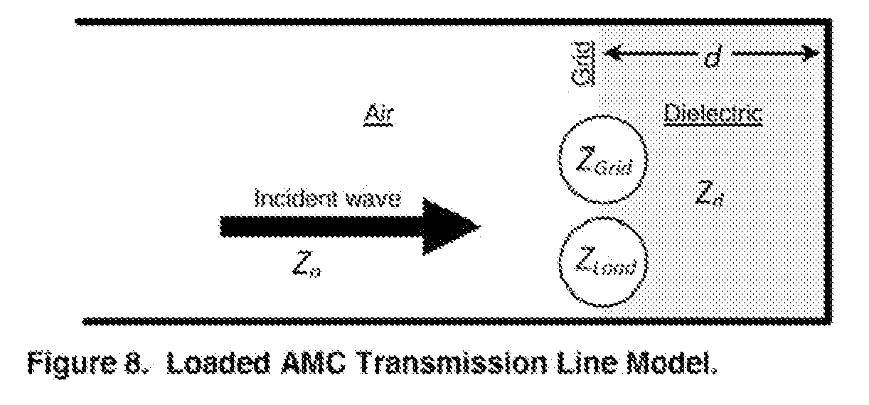
4* AAMC Measurement
The AAMC test articles are fabricated using the architecture shown in Fig. 3 with an array of metallic patches on top of a grounded foam dielectric substrate. The NFCs are connected between the patches. Four control lines for ground, tuning bias, and power are connected from the NFC to a four-plane bias board behind the ground plane. Each NFC requires 32 mW of power. The bias lines pass through hole* in the ground plane, and are RF coupled to the ground plane with 100 pF capacitors to prevent RF coupling between neighboring unit cells. Vias from each patch to ground provide a ground at each terminal of the NFC. The AAMC only operate for a single polarization of incident waves because they are assembled with the MFCs along a single direction. A polarization^ ridepemlent AAMC could be made by installing NPCs along both directions.
It is desirable to measure AMC reflection properties with transverse electromagnetic (TEM) waves. We have measured the AAMC using both a large VHF-UHF parallel-plate TEM cell (LLTC) (Fig. 9a) and a compact coaxial TEM cell (Fig. 9b). The corresponding AMC test articles for each TEM cell are shown In Fig, 10a and Fig. 10b respectively.
The AAMC tested in the PFTC is a 30 cm x 60 cm rectangular panel with 32 unit cells and 32 NPCs. Testing in the PPTC is desirable because it measures the AMC in a finite size that best represents how it will be used in antenna applications. The disadvantages of PPTC testing is that it is costly, labor intensive, and the panel AMC is more expensive to make since it requires 32 elements vs. 8 for the coaxial version. PPTC data extraction requires method -of-momen ts post processing that fits the data to a selected AMC circuit model.
We developed the coaxial TEM cell in order to make rapid measurements of the AAMC 11 ). The coaxial TEM cell has an advantage over parallel plate waveguide TEM cell in that it produces direct real-time measurements of AMC phase and amplitude vs. frequency. The coax AMC appears to the incident wave in the coax as an infinite array of unit cells because of s radial periodicity and the PEC boundaries on coax walla. The
coax TEM cell is a tapered coaxial transmission line terminated by a standard 50-ohm coaxial connector at the small-diameter end and a straight coaxial section at the large* diameter end that accepts the device under test (DUT). The 0-cm Long taper fa formed with two concentric metal cones held in place by low-permittivity structural foam spacers at either end. The taper maintains the 50-ohm transmission fine impedance from end to end.

Fig. 12 shows measurements of a coax AAMC test article that confirms the predicted behavior and validates the NFC stability and operation. Fig. 12 shows several AMC phase curves for various NFC settings. When tuned to the target resonant frequency of 300 MHz* (represented by the bold line in Fig. 12a), the ±90° bandwidth is more than 100% spanning the range from 200 to 450 MHz. A discontinuity in the phase curves between 450 and 600 MHz suggest the onset of coupling to the TBI 1 mode in the coax AMC. The resonant frequency is tunable from 500 MHz down to a limit of 200 MHz before instability in the NFC dominates the performance. A resonant frequency less than 250 MHz, the instability is evident in the loss of smoothness in the phase curves. The instability has been confirmed by measuring radiation from the AMC surface in the extreme tuning range.


Figure 12b compares the ±90° bandwidth of the varac tor-loaded AMC and the NFC- loaded AMC. As predicted by Eqns. 2, 4, and 6, the bandwidth of the varactor-loaded AMC decreases with resonant frequency while the NFC bandwidth increases significantly. The NFC AMC has better than ten times the bandwidth of the varaetor- loaded AMC at high loading levels.
A second AAMC was fabricated using the NFCs whose equivalent circuit parameters ate plotted in Fig. 6. The measurements are compared to simulations of the AAMC using the equivalent circuit parameters extracted in Fig. 13, The simulated resonant frequency is lower than the measured, but the character of the phase curves is similar. It's notable that the net reflection gain predicted for f > 300 MH_* is confirmed by the measurements.
The rectangular panel AAMC seen in Fig. 10 was measured in the parallel-plate TEM cell. The preliminary results are shown in Fig. 14. The data shown here is extracted from a post-processing method that curve firs the measured data to an AAMC circuit model using a method of moments simulation of the scattering in the TEM cell by the AAMC. The results are similar in character to the coax AAMC results. t shows a controllable tuning of the AAMC over more than 100 MHZ, and the phase curves show band widths as much as 50%. The reflection shows a net gain for f<400 MHz for some bias levels. They differ in that the resonant frequency is higher and the tuning range is lower. The differences may be attributable to the effects of the finite size of the AAMC panel which may be presenting different AMC impedance to the NFCs on different locations on the parte] , Another factor may be that the incident power used in the PPTC was too high and drove the NFCs into nonlinear response. Measurement in the coax TEM cell with different power levels confirm this behavior.

Figure 13. Coax AAMC #2 meaturement (left) Mid elmufatlon (right), Tit* simulations are made ualrtg the extracted NFC equivalent circuit paramatera of RQ.6. Tha tuning rang* la lower for the elmulatad data. If a notable that the predicted gain for f < 300 MHx la confirmed by the measurements

5. AAMC Ground Planes
AMCs are touted as substrates that enable low-profile antennas |3]-[¾] because of their magnetic boundary conditions. We tested that hypothesis with our c ax AAMC being used as a ground plane for an antenna mounted 13 mm above it. We have demonstrated that the AAMC does indeed act as a magnetic conductor ground plane and facilitates the placement of antennas very close to its surface.
The antenna measurement setup is seen in Fig. 15. The antenna is a coaxial slot antenna that radiates into the TBM mode of the coax TBM cell. It is excited with the
conductors of a coaxial cable soldered to either side of the slot. The coax slot antenna's; radiation in the coax TEM cell was characteri2ed by measuring the two port S~ parameters; port one is the feed coax cable of the slot antenna and port 2 is the coax output at the top of the coax TEM cell. When the same antenna is mounted 13 mm above a metal plate, no power at all radiates into the coa , and all of the power is reflected back into the feed port. Fig. 15b shows plots of the measured input reflection and the transmission coefficient for the coax slot antenna backed by the AAMC for different bias voltages. For each setting, there is a wide frequency band over which power is radiated efficiently through the coax TEM cell. At some points, the S21>0 dB because of net gain in the NFCs.
A* the NFC bias in increased, Us negative inductance is increased from -70 to -45 nH, and the AA s resonant frequency deceases accordingly. It's reasonable to assume, (although we haven't done rigid analysts on it yet) that the AAMCs resonant frequency is where the antenna's SI I is at a minimum. It's interesting to note that the apparent resonant frequency in this measurement ranges from 150 MHz to 300 MHz, while direct measurements of the AAMC range (see e.g. Fig. 12) from 250 MHz to 500 MHz for the same bias settings. This is because the presence of the large metal region of the antenna adds capacitive Loading to the AAMC, resulting in the operating frequency band shifted lower in frequ icy. This is wmftrmed through simulations or application of Die circuit model of section 3.
The antenna capacitance also shifts the range of NFC stability to a wider range of bias voltages (and more negative inductance). We hypothesize that the extra capacitance added to the AAMC by the antenna enhances the NFC stability.

Rgure 18: a.) The coax slot antenna and the measurement setup in the coax TEM cell, b.) The return tots (top) and the transmitted power of the coax slot antenna when mounted 19 mm above the AAMC ground plane for various AAMC Nee setting*.
6. Conclusions
The work presented here represents what we believe to be the first cteinomtration of Active AMCs loaded with ncm-Foster circuits. The key challenge to realising this was in developing a stable negative inductor which was physically small, low power consuming was producible in large quantities, and capable of being integrating into a passive AMC structure without becoming unstable.
We have convincingly shown that AAMCs caw be tuned over a large frequency range, have bandwidth* in excess of 100% and can be used as magnetic ground planes for low- profile antennas. We have also demonstrated a new method for direct measurement of AMC structures.
AAM technology disclosed here is applicable applicability to a number antenna applications including including 1) Reducing finite ground plane edge affects for antennas mounted on structures to improve their radiation pattern or scattering properties, 2) Reducing coupling between closely spaced (< 1 λ) antenna elements on structures to mitigate co-site interference, 3) Enable radiation of energy polarized parallel to and directed along structural metal surfaces, and 4) Increase the bandwidth and efficiency of cavity-backed slot antennas while reducing cavity size.
While non-Foster circuit technology offers the potential to overcome fundamental limits on bandwidth and electrical .size as demonstrated with the AAMC, it has many other electromagnetic applications (e.g. antenna matching, mctamatcrials). Of course, NFC stability will remain a large issue and needs to be addressed in setail for any application. We achieved stability through simultaneous circuit and AMC design that paid careful attention to parasitica in the circuit realization and the electromagnetic loading imposed by antenna geometry, metamaterial configuration, environment surrounding and bias network. This enabled stability robustness by enabling compensation for real world fabrication tolerance and uncontrollable surrounding environment loadings that must be compensated for in practical realtftations.
Other applications for negative inductor non-Foster circuit developed on this project include 1) Wideband reactance cancellation of VHF UHF slot antennas, 2) Realization of wideband adaptable VHF UHF artificial impedance surfaces, both scalar and tensor, for holographic artificial impedance surface antennas or control of surface wave propagation on. surf aces, and 3) Realization of wideband, thin, lightweight Salisbury screens/Iaumann absorbers.
Further research necessary general maturation of non-Foster technology 1) Study of the noise characteristic and ways to minimise it for receive applications, 2) Power handlin for transmit applications, 3) Increased linearity , and 4) Self adaptive control to maintain stability in a changing environment, Solutions to these challenges will require more work in the area of optimum circuit topologies and considerali<m of ΠΙ V (e.g., InP and GaN) semiconductor technologies which offer inherent electrical property advantages (eg., electron mobility, larger bandgaps) relative to Si.
7. Acknowledgements
The material in this paper is based upon work supported by the Air Force under AFRL Contract No. FA87lt O«C«0007. Any opinions, findings und conclusions or recommcpdations expressed in this material are those of the authors' and do not necessarily reflect the views of the AFRL.
8· eferences
[1) R. M, Poster,, "A reactance theorem", Bell Systems Technical Journal, vol J, pp.
259-267, 1924.
[2] C. R. White , J, S. Colburn and R. O. Nagelc, "A Non-Foster~Enhanccd Monopole Antenna" AP-URSI conference, July 7, 201 1
t3] D. J, Cregoirc, C. R, White, J, S. Colburn, and G, P, Johnson, "Variable UHF-Band Artificial Magnetic Conductors", Proceedings of the 2010 Antenna Applications Symposium, (AAS-2010), Allerton Park, U, pp 150-165
(4) A.P. Feres idis, G. Goussetis, S. Wang, J.C. Vardaxoglou, "Artificial magnetic conductor surface* and their application to low -profile, high-gain planar antennas", IEEE Trans. Antennas Prupag., vj55, DO. l . p. 209*215, Jan 2005
[5] $ JR. Best and D.L. Hanna, "Desi n of a broadband dipole in close proximity to an EBC ground plane", IEEE Ant. And Prop. Mag., 50, 2, 2008
(6| F. Yang and Y. Rahraat-Samii, "Electromagnetic Band-Gap Structure* in Antenna Engineering", ser, The Cambridge RF and Microwave Engineering Series. Cambridge, U J ,: Cambridge Univ. Press, 2008.
[7] J JR. Sohn, .Y. Kim, and H.-S. Tae, "Comparative study on various artificial magnetic conductors for low-profile anten a", Prog. Elect. Res., (1„ 7, 2006
[8] L Akhoondzadch-Asl, DJ. Kern, Peter S. Hall, and D.H. Werner, "Wideband Dipoles on Electromagnetic Bandgap Ground Planer", IEEE Trans. Ant. Prop., 55, 2426, 2007
(9) R. D. Middlebrook, "Measurement of Loop Gain in Feedback Systems," International Journal of Electronics, 38(4), April 1975, 4*5«512
110] C. R, White, J, W. May and J. S, Colburn, "A variable negative-inductance integrated circuit at UHF frequencies'*, submitted to IEEE Microwave and Wireless Component Letters, 2011
[llj . Sirnovskii et al , "High-impedance surfaces having stable resonance with respect to polarization and incidence angle*', IEEE Trans. Antennas Prop., 53, 08, 2005 f 12] O. Luukkoncn et al, "Simple and accurate analytical model of planar grids and high< impedance surfaces'*, IEEE Trans. Antennas Prop., vol. 56, 1624, 008
[131 D. J. Gr goire and C. K, White, "Direct measurement of artificial magnetic conductors", submitted to AMTA 2 1 1
Claims
1. A tunable impedance surface, the tunable surface comprising: (a) a plurality of elements disposed in a two dimensional array; and (b) an arrangement of variable negative reactance circuits for controllably varying negative reactance between at least selected ones of adjacent elements in said two dimensional array.
2. The tunable impedance surface of claim 1 further including a substrate having first and second major surfaces, said substrate supporting a ground plane on the first major surface thereof and supporting said plurality of elements and the arrangement of variable negative reactance circuits on the second major surface thereof, the substrate having a thickness such that a distance between the ground plane and said plurality of elements is less than a wavelength of a radio frequency of interest.
3. The tunable impedance surface of claim 2 wherein the arrangement of variable negative reactance circuits is adjustable in response to one or more control signals to spatially tune the tunable impedance surface.
4. The tunable impedance surface of claim 3 wherein the plurality of elements each have an outside diameter which is less than the wavelength of the radio frequency of interest.
5. The tunable impedance surface of claim 1 wherein the elements are directly or ohmically coupled to the ground plane by vias in a substrate supporting said ground plane, said plurality of elements and said arrangement of variable negative reactance circuits.
6. The tunable impedance surface of claim 1 further including a substrate having two major surfaces, said substrate supporting supporting said plurality of elements and the arrangement of variable negative reactance circuits on a common major surface thereof.
7. The tunable impedance surface of claim 6 wherein the arrangement of variable negative reactance circuits each have an adjustable negative reactance which is controlled by a control signal for spatially tuning the tunable impedance surface.
8. The tunable impedance surface of claim 1 wherein the arrangement of variable negative reactance circuits comprises a plurality of negative reactance integrated circuits, each negative reactance integrated circuit of said plurality of negative reactance integrated circuits being coupled between adjacent ones of said plurality of elements.
9. The tunable impedance surface of claim 1 wherein the negative reactance circuits in said arrangement of variable negative reactance circuits are each controlled by a control voltage.
10. The tunable impedance surface of claim 1 wherein the negative reactance circuits in said arrangement of variable negative reactance circuits each comprise two pairs of differentially coupled transistors, a capacitor coupled between current carrying electrodes of a first pair of said two pairs of differentially coupled transistors with a negative reactance being realized between currently carrying electrodes of a second pair of said two pairs of differentially coupled transistors.
11. The tunable impedance surface of claim 1 wherein the negative reactance circuits in said arrangement of variable negative reactance circuits each comprise:
two pairs of cross-coupled transistors;
a reactive load coupled to first current carrying electrodes of a first one of the pairs of cross-coupled transistors and a first control resistance coupled to second current carrying electrodes of said first one of the pairs of cross-coupled transistors;
a second control resistance coupled to current carrying electrodes current carrying electrodes of a second one of the pairs of cross-coupled transistors;
current sources for suppling a flow of current to at least one of the current carrying electrodes of each pair of cross-coupled transistors;
two common-mode feedback networks, each common-mode feedback network being coupled to current carrying electrodes of each pair of cross-coupled transistors; and
terminals coupled to current carrying electrodes of said second one of the pairs of cross- coupled transistors, a function of the product of the resistances of the first and second control resistances setting a conversion ratio between the reactive load and a load appearing across said terminals, said terminals being coupled to at least selected ones of said adjacent elements in said two dimensional array.
12. The tunable impedance surface of claim 1 wherein the negative reactance is a negative inductance.
Priority Applications (2)
| Application Number | Priority Date | Filing Date | Title |
|---|---|---|---|
| EP12767559.3A EP2695241B1 (en) | 2011-04-07 | 2012-04-06 | Tunable impedance surfaces |
| CN201280021746.XA CN103548205B (en) | 2011-04-07 | 2012-04-06 | Tunable impedance surfaces |
Applications Claiming Priority (10)
| Application Number | Priority Date | Filing Date | Title |
|---|---|---|---|
| US201161473076P | 2011-04-07 | 2011-04-07 | |
| US61/473,076 | 2011-04-07 | ||
| US201161505037P | 2011-07-06 | 2011-07-06 | |
| US61/505,037 | 2011-07-06 | ||
| US201161537488P | 2011-09-21 | 2011-09-21 | |
| US61/537,488 | 2011-09-21 | ||
| US13/441,659 US8976077B2 (en) | 2011-04-07 | 2012-04-06 | Widebrand adaptable artificial impedance surface |
| US13/441,730 US8988173B2 (en) | 2011-04-07 | 2012-04-06 | Differential negative impedance converters and inverters with variable or tunable conversion ratios |
| US13/441,659 | 2012-04-06 | ||
| US13/441,730 | 2012-04-06 |
Publications (2)
| Publication Number | Publication Date |
|---|---|
| WO2012139079A2 true WO2012139079A2 (en) | 2012-10-11 |
| WO2012139079A3 WO2012139079A3 (en) | 2013-02-28 |
Family
ID=46965676
Family Applications (1)
| Application Number | Title | Priority Date | Filing Date |
|---|---|---|---|
| PCT/US2012/032648 WO2012139079A2 (en) | 2011-04-07 | 2012-04-06 | Tunable impedance surfaces |
Country Status (4)
| Country | Link |
|---|---|
| US (2) | US8976077B2 (en) |
| EP (1) | EP2695241B1 (en) |
| CN (1) | CN103548205B (en) |
| WO (1) | WO2012139079A2 (en) |
Cited By (3)
| Publication number | Priority date | Publication date | Assignee | Title |
|---|---|---|---|---|
| WO2014182398A1 (en) * | 2013-05-07 | 2014-11-13 | Board Of Regents, The University Of Texas System | Circuit-loaded conformal metasurface cloak |
| CN106058445A (en) * | 2016-07-26 | 2016-10-26 | 中国科学院国家空间科学中心 | Three-layer metal plate based broadband transmission array antenna |
| US11024952B1 (en) | 2019-01-25 | 2021-06-01 | Hrl Laboratories, Llc | Broadband dual polarization active artificial magnetic conductor |
Families Citing this family (88)
| Publication number | Priority date | Publication date | Assignee | Title |
|---|---|---|---|---|
| EP2695241B1 (en) * | 2011-04-07 | 2021-08-18 | HRL Laboratories, LLC | Tunable impedance surfaces |
| US9407239B2 (en) | 2011-07-06 | 2016-08-02 | Hrl Laboratories, Llc | Wide bandwidth automatic tuning circuit |
| WO2015047421A1 (en) | 2013-09-30 | 2015-04-02 | Hrl Laboratories, Llc | Normally-off iii-nitride transistors with high threshold-voltage and low on-resistance |
| US9715953B2 (en) | 2012-02-13 | 2017-07-25 | The University Of North Carolina At Charlotte | Wideband negative-permittivity and negative-permeability metamaterials utilizing non-foster elements |
| US10103445B1 (en) * | 2012-06-05 | 2018-10-16 | Hrl Laboratories, Llc | Cavity-backed slot antenna with an active artificial magnetic conductor |
| US9867062B1 (en) | 2014-07-21 | 2018-01-09 | Energous Corporation | System and methods for using a remote server to authorize a receiving device that has requested wireless power and to determine whether another receiving device should request wireless power in a wireless power transmission system |
| US10439448B2 (en) | 2014-08-21 | 2019-10-08 | Energous Corporation | Systems and methods for automatically testing the communication between wireless power transmitter and wireless power receiver |
| US9871398B1 (en) | 2013-07-01 | 2018-01-16 | Energous Corporation | Hybrid charging method for wireless power transmission based on pocket-forming |
| US10992187B2 (en) | 2012-07-06 | 2021-04-27 | Energous Corporation | System and methods of using electromagnetic waves to wirelessly deliver power to electronic devices |
| US11502551B2 (en) | 2012-07-06 | 2022-11-15 | Energous Corporation | Wirelessly charging multiple wireless-power receivers using different subsets of an antenna array to focus energy at different locations |
| US10063105B2 (en) | 2013-07-11 | 2018-08-28 | Energous Corporation | Proximity transmitters for wireless power charging systems |
| US10256657B2 (en) | 2015-12-24 | 2019-04-09 | Energous Corporation | Antenna having coaxial structure for near field wireless power charging |
| US10381880B2 (en) * | 2014-07-21 | 2019-08-13 | Energous Corporation | Integrated antenna structure arrays for wireless power transmission |
| US9787103B1 (en) | 2013-08-06 | 2017-10-10 | Energous Corporation | Systems and methods for wirelessly delivering power to electronic devices that are unable to communicate with a transmitter |
| US10965164B2 (en) | 2012-07-06 | 2021-03-30 | Energous Corporation | Systems and methods of wirelessly delivering power to a receiver device |
| US10992185B2 (en) | 2012-07-06 | 2021-04-27 | Energous Corporation | Systems and methods of using electromagnetic waves to wirelessly deliver power to game controllers |
| US9876394B1 (en) | 2014-05-07 | 2018-01-23 | Energous Corporation | Boost-charger-boost system for enhanced power delivery |
| JP6373010B2 (en) * | 2013-03-12 | 2018-08-15 | キヤノン株式会社 | Oscillating element |
| US20150244079A1 (en) * | 2014-02-24 | 2015-08-27 | Hrl Laboratories, Llc. | Cavity-backed artificial magnetic conductor |
| US9705201B2 (en) | 2014-02-24 | 2017-07-11 | Hrl Laboratories, Llc | Cavity-backed artificial magnetic conductor |
| US9425769B1 (en) | 2014-07-18 | 2016-08-23 | Hrl Laboratories, Llc | Optically powered and controlled non-foster circuit |
| US10116143B1 (en) | 2014-07-21 | 2018-10-30 | Energous Corporation | Integrated antenna arrays for wireless power transmission |
| US10068703B1 (en) | 2014-07-21 | 2018-09-04 | Energous Corporation | Integrated miniature PIFA with artificial magnetic conductor metamaterials |
| US10193233B1 (en) * | 2014-09-17 | 2019-01-29 | Hrl Laboratories, Llc | Linearly polarized active artificial magnetic conductor |
| CZ305905B6 (en) * | 2014-10-01 | 2016-04-27 | Univerzita Tomáše Bati ve Zlíně | Thin wideband radio absorber |
| GB2531520B (en) * | 2014-10-20 | 2018-07-18 | Smart Antenna Tech Limited | Antenna impedance matching with negative impedance converters |
| US10031191B1 (en) | 2015-01-16 | 2018-07-24 | Hrl Laboratories, Llc | Piezoelectric magnetometer capable of sensing a magnetic field in multiple vectors |
| JPWO2016121375A1 (en) * | 2015-01-26 | 2017-11-24 | 日本電気株式会社 | Frequency selection surface, radio communication device and radar device |
| US10523033B2 (en) | 2015-09-15 | 2019-12-31 | Energous Corporation | Receiver devices configured to determine location within a transmission field |
| US10186893B2 (en) | 2015-09-16 | 2019-01-22 | Energous Corporation | Systems and methods for real time or near real time wireless communications between a wireless power transmitter and a wireless power receiver |
| US10211685B2 (en) | 2015-09-16 | 2019-02-19 | Energous Corporation | Systems and methods for real or near real time wireless communications between a wireless power transmitter and a wireless power receiver |
| US10778041B2 (en) | 2015-09-16 | 2020-09-15 | Energous Corporation | Systems and methods for generating power waves in a wireless power transmission system |
| US9871387B1 (en) | 2015-09-16 | 2018-01-16 | Energous Corporation | Systems and methods of object detection using one or more video cameras in wireless power charging systems |
| US10734717B2 (en) | 2015-10-13 | 2020-08-04 | Energous Corporation | 3D ceramic mold antenna |
| US10027180B1 (en) | 2015-11-02 | 2018-07-17 | Energous Corporation | 3D triple linear antenna that acts as heat sink |
| US10063108B1 (en) | 2015-11-02 | 2018-08-28 | Energous Corporation | Stamped three-dimensional antenna |
| US10038332B1 (en) | 2015-12-24 | 2018-07-31 | Energous Corporation | Systems and methods of wireless power charging through multiple receiving devices |
| US10079515B2 (en) | 2016-12-12 | 2018-09-18 | Energous Corporation | Near-field RF charging pad with multi-band antenna element with adaptive loading to efficiently charge an electronic device at any position on the pad |
| US10027159B2 (en) | 2015-12-24 | 2018-07-17 | Energous Corporation | Antenna for transmitting wireless power signals |
| US11863001B2 (en) | 2015-12-24 | 2024-01-02 | Energous Corporation | Near-field antenna for wireless power transmission with antenna elements that follow meandering patterns |
| US10116162B2 (en) | 2015-12-24 | 2018-10-30 | Energous Corporation | Near field transmitters with harmonic filters for wireless power charging |
| US10008886B2 (en) | 2015-12-29 | 2018-06-26 | Energous Corporation | Modular antennas with heat sinks in wireless power transmission systems |
| CN106450715A (en) * | 2016-08-23 | 2017-02-22 | 江苏省东方世纪网络信息有限公司 | Dual-polarized antenna and radiation unit thereof |
| US10923954B2 (en) | 2016-11-03 | 2021-02-16 | Energous Corporation | Wireless power receiver with a synchronous rectifier |
| US10177454B1 (en) | 2016-11-04 | 2019-01-08 | Hrl Laboratories, Llc | Lumped element tensor impedance surfaces |
| JP6691273B2 (en) | 2016-12-12 | 2020-04-28 | エナージャス コーポレイション | A method for selectively activating the antenna area of a near-field charging pad to maximize delivered wireless power |
| US10439442B2 (en) | 2017-01-24 | 2019-10-08 | Energous Corporation | Microstrip antennas for wireless power transmitters |
| US10389161B2 (en) | 2017-03-15 | 2019-08-20 | Energous Corporation | Surface mount dielectric antennas for wireless power transmitters |
| US10680319B2 (en) | 2017-01-06 | 2020-06-09 | Energous Corporation | Devices and methods for reducing mutual coupling effects in wireless power transmission systems |
| US11011942B2 (en) | 2017-03-30 | 2021-05-18 | Energous Corporation | Flat antennas having two or more resonant frequencies for use in wireless power transmission systems |
| US10511097B2 (en) | 2017-05-12 | 2019-12-17 | Energous Corporation | Near-field antennas for accumulating energy at a near-field distance with minimal far-field gain |
| CA3063768A1 (en) * | 2017-05-15 | 2018-11-22 | Valorbec Societe En Commandite | Contactless air-filled substrate integrated waveguide devices and methods |
| CN107181056B (en) * | 2017-05-16 | 2022-08-30 | 叶云裳 | Microwave attenuation type GNSS measurement type antenna and equipment |
| US11462949B2 (en) | 2017-05-16 | 2022-10-04 | Wireless electrical Grid LAN, WiGL Inc | Wireless charging method and system |
| CN107275793B (en) * | 2017-05-31 | 2021-02-12 | 南京理工大学 | Frequency-adjustable coplanar compact artificial magnetic conductor structure based on vanadium dioxide film |
| US10848853B2 (en) | 2017-06-23 | 2020-11-24 | Energous Corporation | Systems, methods, and devices for utilizing a wire of a sound-producing device as an antenna for receipt of wirelessly delivered power |
| CN107680576A (en) * | 2017-09-07 | 2018-02-09 | 国家电网公司 | Active frequency follows phonon crystal and its noise-reduction method |
| US10122219B1 (en) | 2017-10-10 | 2018-11-06 | Energous Corporation | Systems, methods, and devices for using a battery as a antenna for receiving wirelessly delivered power from radio frequency power waves |
| US11342798B2 (en) | 2017-10-30 | 2022-05-24 | Energous Corporation | Systems and methods for managing coexistence of wireless-power signals and data signals operating in a same frequency band |
| US10615647B2 (en) | 2018-02-02 | 2020-04-07 | Energous Corporation | Systems and methods for detecting wireless power receivers and other objects at a near-field charging pad |
| US11159057B2 (en) | 2018-03-14 | 2021-10-26 | Energous Corporation | Loop antennas with selectively-activated feeds to control propagation patterns of wireless power signals |
| CN108493602B (en) | 2018-05-22 | 2023-06-20 | 华南理工大学 | Dual-polarized duplex antenna and dual-frequency base station antenna array formed by same |
| US10903569B2 (en) * | 2018-06-15 | 2021-01-26 | Huawei Technologies Co., Ltd. | Reconfigurable radial waveguides with switchable artificial magnetic conductors |
| US11515732B2 (en) | 2018-06-25 | 2022-11-29 | Energous Corporation | Power wave transmission techniques to focus wirelessly delivered power at a receiving device |
| CN109273859B (en) * | 2018-10-17 | 2020-08-11 | 哈尔滨工业大学 | Coupling type broadband active frequency selective surface |
| US11437735B2 (en) | 2018-11-14 | 2022-09-06 | Energous Corporation | Systems for receiving electromagnetic energy using antennas that are minimally affected by the presence of the human body |
| JP7122523B2 (en) * | 2018-12-17 | 2022-08-22 | パナソニックIpマネジメント株式会社 | antenna device |
| US11539243B2 (en) | 2019-01-28 | 2022-12-27 | Energous Corporation | Systems and methods for miniaturized antenna for wireless power transmissions |
| JP2022519749A (en) | 2019-02-06 | 2022-03-24 | エナージャス コーポレイション | Systems and methods for estimating the optimum phase for use with individual antennas in an antenna array |
| CN110034390A (en) * | 2019-04-25 | 2019-07-19 | 北京机电工程研究所 | A kind of thin layer covering of electromagnetic scattering and radiation coordinated regulation |
| CN110289500B (en) * | 2019-04-26 | 2020-10-30 | 中国计量大学上虞高等研究院有限公司 | Adjustable double-frequency terahertz absorber |
| CN110233341A (en) * | 2019-06-14 | 2019-09-13 | 西安电子科技大学 | A kind of broadband dual polarized antenna of line of rabbet joint low section |
| CN110504527B (en) * | 2019-07-31 | 2020-11-17 | 电子科技大学 | L and X wave band common-caliber antenna with novel structure |
| US11381118B2 (en) | 2019-09-20 | 2022-07-05 | Energous Corporation | Systems and methods for machine learning based foreign object detection for wireless power transmission |
| WO2021055900A1 (en) | 2019-09-20 | 2021-03-25 | Energous Corporation | Classifying and detecting foreign objects using a power amplifier controller integrated circuit in wireless power transmission systems |
| WO2021055898A1 (en) | 2019-09-20 | 2021-03-25 | Energous Corporation | Systems and methods for machine learning based foreign object detection for wireless power transmission |
| US11411441B2 (en) | 2019-09-20 | 2022-08-09 | Energous Corporation | Systems and methods of protecting wireless power receivers using multiple rectifiers and establishing in-band communications using multiple rectifiers |
| WO2021119483A1 (en) | 2019-12-13 | 2021-06-17 | Energous Corporation | Charging pad with guiding contours to align an electronic device on the charging pad and efficiently transfer near-field radio-frequency energy to the electronic device |
| US10985617B1 (en) | 2019-12-31 | 2021-04-20 | Energous Corporation | System for wirelessly transmitting energy at a near-field distance without using beam-forming control |
| CN111430891B (en) * | 2020-03-13 | 2021-09-21 | 华南理工大学 | Broadband low-profile antenna based on polarization correlation super-surface structure |
| US11799324B2 (en) | 2020-04-13 | 2023-10-24 | Energous Corporation | Wireless-power transmitting device for creating a uniform near-field charging area |
| CN111666731B (en) * | 2020-06-05 | 2022-07-12 | 电子科技大学 | Ultrathin ultra-wideband flat wave absorber based on non-Foster circuit and design method thereof |
| US11837785B2 (en) * | 2020-08-04 | 2023-12-05 | Sony Group Corporation | Holographic antenna and holographic antenna arrangement |
| US11988740B2 (en) | 2020-09-08 | 2024-05-21 | Anduril Industries, Inc. | Millimeter wavelength radar antenna for drone interception |
| KR102413884B1 (en) * | 2021-05-26 | 2022-06-30 | 성균관대학교산학협력단 | Reflective Intelligent Reflecting Surfaces flexible board |
| CN114039203B (en) * | 2021-11-10 | 2022-10-04 | 大连理工大学 | Novel low-profile dual-polarized base station antenna |
| US11916398B2 (en) | 2021-12-29 | 2024-02-27 | Energous Corporation | Small form-factor devices with integrated and modular harvesting receivers, and shelving-mounted wireless-power transmitters for use therewith |
| WO2024084813A1 (en) * | 2022-10-21 | 2024-04-25 | Mitsubishi Electric Corporation | Passive negative inductor and a method for fabricating the passive negative inductor |
Family Cites Families (62)
| Publication number | Priority date | Publication date | Assignee | Title |
|---|---|---|---|---|
| US4234960A (en) | 1978-07-03 | 1980-11-18 | Ashton James Spilsbury | Antenna automatic tuning apparatus |
| US4990872A (en) | 1987-06-17 | 1991-02-05 | Sanyo Electric Co., Ltd. | Variable reactance circuit producing negative to positive varying reactance |
| JP2766264B2 (en) | 1987-10-12 | 1998-06-18 | 株式会社東芝 | Differential amplifier circuit |
| US5392002A (en) | 1993-05-28 | 1995-02-21 | National Semiconductor Corporation | Low voltage bipolar negative impedance converter |
| GB2288502A (en) | 1994-04-14 | 1995-10-18 | Northern Telecom Ltd | Voltage controlled oscillator |
| US5489878A (en) | 1994-11-23 | 1996-02-06 | Analog Devices | Current-controlled quadrature oscillator based on differential gm /C cells |
| US6121940A (en) | 1997-09-04 | 2000-09-19 | Ail Systems, Inc. | Apparatus and method for broadband matching of electrically small antennas |
| DE19808377B4 (en) * | 1998-02-27 | 2005-08-04 | Infineon Technologies Ag | Fully integrated voltage controlled oscillator circuit |
| JP3884958B2 (en) | 1999-10-13 | 2007-02-21 | 株式会社日立製作所 | Communication terminal, in-vehicle communication terminal, and vehicle using the same |
| US7388186B2 (en) | 1999-10-28 | 2008-06-17 | Hrl Laboratories, Llc | Optically controlled MEMS devices |
| US6483480B1 (en) | 2000-03-29 | 2002-11-19 | Hrl Laboratories, Llc | Tunable impedance surface |
| US6538621B1 (en) * | 2000-03-29 | 2003-03-25 | Hrl Laboratories, Llc | Tunable impedance surface |
| US6518930B2 (en) | 2000-06-02 | 2003-02-11 | The Regents Of The University Of California | Low-profile cavity-backed slot antenna using a uniplanar compact photonic band-gap substrate |
| DE10129850B4 (en) | 2000-07-20 | 2016-12-29 | Siemens Healthcare Gmbh | Amplifier device with frequency response compensating amplifier reactance and use of the amplifier device |
| US6411261B1 (en) * | 2001-02-26 | 2002-06-25 | E-Tenna Corporation | Artificial magnetic conductor system and method for manufacturing |
| US6525695B2 (en) * | 2001-04-30 | 2003-02-25 | E-Tenna Corporation | Reconfigurable artificial magnetic conductor using voltage controlled capacitors with coplanar resistive biasing network |
| US6897831B2 (en) * | 2001-04-30 | 2005-05-24 | Titan Aerospace Electronic Division | Reconfigurable artificial magnetic conductor |
| US6731241B2 (en) | 2001-06-13 | 2004-05-04 | Raytheon Company | Dual-polarization common aperture antenna with rectangular wave-guide fed centered longitudinal slot array and micro-stripline fed air cavity back transverse series slot array |
| US6476771B1 (en) | 2001-06-14 | 2002-11-05 | E-Tenna Corporation | Electrically thin multi-layer bandpass radome |
| US6608603B2 (en) | 2001-08-24 | 2003-08-19 | Broadcom Corporation | Active impedance matching in communications systems |
| US6917343B2 (en) * | 2001-09-19 | 2005-07-12 | Titan Aerospace Electronics Division | Broadband antennas over electronically reconfigurable artificial magnetic conductor surfaces |
| US6509875B1 (en) | 2001-09-19 | 2003-01-21 | Motorola, Inc. | Electronically tuned active antenna apparatus |
| US7187913B1 (en) | 2002-01-25 | 2007-03-06 | Sige Semiconductor Inc. | Integrated circuit tuner with broad tuning range |
| US7420524B2 (en) | 2003-04-11 | 2008-09-02 | The Penn State Research Foundation | Pixelized frequency selective surfaces for reconfigurable artificial magnetically conducting ground planes |
| US7245269B2 (en) * | 2003-05-12 | 2007-07-17 | Hrl Laboratories, Llc | Adaptive beam forming antenna system using a tunable impedance surface |
| US7071888B2 (en) * | 2003-05-12 | 2006-07-04 | Hrl Laboratories, Llc | Steerable leaky wave antenna capable of both forward and backward radiation |
| WO2005031911A2 (en) | 2003-08-01 | 2005-04-07 | The Penn State Research Foundation | High-selectivity electromagnetic bandgap device and antenna system |
| JP4469632B2 (en) | 2004-02-24 | 2010-05-26 | 富士通株式会社 | Control device for antenna matching circuit |
| WO2006034311A2 (en) | 2004-09-20 | 2006-03-30 | The Trustees Of Columbia University In The City Of New York | Low voltage track and hold circuits |
| US8111111B2 (en) | 2004-11-19 | 2012-02-07 | Epcos Ag | Device comprising a controlled matching stage |
| US7586384B2 (en) | 2005-08-15 | 2009-09-08 | Nokia Corporation | Integrated load impedance sensing for tunable matching networks |
| US7683854B2 (en) * | 2006-02-09 | 2010-03-23 | Raytheon Company | Tunable impedance surface and method for fabricating a tunable impedance surface |
| FR2905041A1 (en) | 2006-08-17 | 2008-02-22 | St Microelectronics Sa | Negative capacitance circuit for forming voltage controlled oscillator, has two branches connected between two reference potentials, and linearizing resistor parallely connected between two emitter electrodes of bipolar transistors |
| US7525500B2 (en) | 2006-10-20 | 2009-04-28 | Agilent Technologies, Inc. | Element reduction in phased arrays with cladding |
| JPWO2008050441A1 (en) | 2006-10-26 | 2010-02-25 | パナソニック株式会社 | Antenna device |
| RU2451946C2 (en) | 2006-12-22 | 2012-05-27 | Конинклейке Филипс Электроникс Н.В. | Radio-frequency coil for use in magnetic resonance imaging system |
| US20080164955A1 (en) | 2007-01-04 | 2008-07-10 | Pfeiffer Ullrich R | Voltage controlled oscillator circuits and methods using variable capacitance degeneration for increased tuning range |
| US7541982B2 (en) | 2007-03-05 | 2009-06-02 | Lockheed Martin Corporation | Probe fed patch antenna |
| US7764932B2 (en) | 2007-03-14 | 2010-07-27 | Broadcom Corporation | Antenna system for use within a wireless communication device |
| JP2008278159A (en) | 2007-04-27 | 2008-11-13 | General Research Of Electronics Inc | Variable capacitance circuit |
| US20080284674A1 (en) * | 2007-05-15 | 2008-11-20 | Hrl Laboratories, Llc | Digital control architecture for a tunable impedance surface |
| RU2379800C2 (en) | 2007-07-25 | 2010-01-20 | Самсунг Электроникс Ко., Лтд. | Electromagnetic shield with large surface impedance |
| US7880568B2 (en) | 2007-09-17 | 2011-02-01 | Oracle America, Inc. | Equalizer system having a tunable active inductor |
| FR2926689A1 (en) | 2008-01-18 | 2009-07-24 | Commissariat Energie Atomique | ELECTRICAL DEVICE WITH RESONATOR WITH BROAD RANGE OF FREQUENCY VARIATION |
| GB2457103B (en) | 2008-01-31 | 2010-11-03 | Brandenburg | An insect trap |
| US7924096B2 (en) | 2009-03-06 | 2011-04-12 | Analog Devices, Inc. | Input buffer with impedance cancellation |
| CN105226396B (en) | 2009-03-12 | 2019-04-12 | 泰科电子服务股份有限公司 | Mostly with the compound right hand and left hand (CRLH) slot antenna |
| US20100238085A1 (en) | 2009-03-23 | 2010-09-23 | Toyota Motor Engineering & Manufacturing North America, Inc. | Plastic waveguide slot array and method of manufacture |
| US8451189B1 (en) | 2009-04-15 | 2013-05-28 | Herbert U. Fluhler | Ultra-wide band (UWB) artificial magnetic conductor (AMC) metamaterials for electrically thin antennas and arrays |
| US8263939B2 (en) * | 2009-04-21 | 2012-09-11 | The Boeing Company | Compressive millimeter wave imaging |
| FR2949612A1 (en) | 2009-08-28 | 2011-03-04 | Thomson Licensing | ANTENNA SYSTEM COMPRISING AN ELECTRICALLY SMALL ANTENNA FOR RECEIVING CHANNEL SIGNALS FROM THE UHF BAND |
| US9093753B2 (en) * | 2010-01-22 | 2015-07-28 | Industry-Academic Cooperation Foundation, Yonsei University | Artificial magnetic conductor |
| US8957831B1 (en) * | 2010-03-30 | 2015-02-17 | The Boeing Company | Artificial magnetic conductors |
| CN101853974A (en) * | 2010-04-07 | 2010-10-06 | 北京航空航天大学 | Ultra wide band submillimeter-wave frequency selection surface |
| US9203158B2 (en) | 2010-04-11 | 2015-12-01 | Broadcom Corporation | Programmable antenna having metal inclusions and bidirectional coupling circuits |
| JP4998582B2 (en) | 2010-04-16 | 2012-08-15 | 株式会社日本自動車部品総合研究所 | Wireless communication device |
| US8374561B1 (en) | 2010-04-27 | 2013-02-12 | Hrl Laboratories, Llc | Non-foster impedance power amplifier |
| US8436785B1 (en) * | 2010-11-03 | 2013-05-07 | Hrl Laboratories, Llc | Electrically tunable surface impedance structure with suppressed backward wave |
| EP2695241B1 (en) * | 2011-04-07 | 2021-08-18 | HRL Laboratories, LLC | Tunable impedance surfaces |
| US20130009720A1 (en) | 2011-07-06 | 2013-01-10 | Hrl Laboratories, Llc | Wide bandwidth automatic tuning circuit |
| EP2695296B1 (en) | 2011-04-07 | 2020-07-15 | HRL Laboratories, LLC | Non-foster circuit |
| US9407239B2 (en) | 2011-07-06 | 2016-08-02 | Hrl Laboratories, Llc | Wide bandwidth automatic tuning circuit |
-
2012
- 2012-04-06 EP EP12767559.3A patent/EP2695241B1/en active Active
- 2012-04-06 CN CN201280021746.XA patent/CN103548205B/en active Active
- 2012-04-06 WO PCT/US2012/032648 patent/WO2012139079A2/en active Application Filing
- 2012-04-06 US US13/441,659 patent/US8976077B2/en active Active
-
2014
- 2014-02-24 US US14/188,225 patent/US9379448B2/en active Active
Non-Patent Citations (1)
| Title |
|---|
| See references of EP2695241A4 * |
Cited By (3)
| Publication number | Priority date | Publication date | Assignee | Title |
|---|---|---|---|---|
| WO2014182398A1 (en) * | 2013-05-07 | 2014-11-13 | Board Of Regents, The University Of Texas System | Circuit-loaded conformal metasurface cloak |
| CN106058445A (en) * | 2016-07-26 | 2016-10-26 | 中国科学院国家空间科学中心 | Three-layer metal plate based broadband transmission array antenna |
| US11024952B1 (en) | 2019-01-25 | 2021-06-01 | Hrl Laboratories, Llc | Broadband dual polarization active artificial magnetic conductor |
Also Published As
| Publication number | Publication date |
|---|---|
| WO2012139079A3 (en) | 2013-02-28 |
| CN103548205A (en) | 2014-01-29 |
| EP2695241A2 (en) | 2014-02-12 |
| US8976077B2 (en) | 2015-03-10 |
| US20150244080A1 (en) | 2015-08-27 |
| EP2695241B1 (en) | 2021-08-18 |
| US9379448B2 (en) | 2016-06-28 |
| EP2695241A4 (en) | 2014-08-27 |
| CN103548205B (en) | 2017-02-22 |
| US20120256811A1 (en) | 2012-10-11 |
Similar Documents
| Publication | Publication Date | Title |
|---|---|---|
| EP2695241A2 (en) | Tunable impedance surfaces | |
| Gregoire et al. | Wideband artificial magnetic conductors loaded with non-Foster negative inductors | |
| Yoo et al. | Polarization-independent and ultrawideband metamaterial absorber using a hexagonal artificial impedance surface and a resistor-capacitor layer | |
| US6906682B2 (en) | Apparatus for generating a magnetic interface and applications of the same | |
| Mias et al. | A varactor-tunable high impedance surface with a resistive-lumped-element biasing grid | |
| US8633866B2 (en) | Frequency-selective surface (FSS) structures | |
| Mirzaei et al. | A resonant printed monopole antenna with an embedded non-Foster matching network | |
| US20030142036A1 (en) | Multiband or broadband frequency selective surface | |
| Long et al. | Broadband fast-wave propagation in a non-Foster circuit loaded waveguide | |
| Wang et al. | Low cross-polarization ultrawideband tightly coupled balanced antipodal dipole array | |
| CN111478050B (en) | Flexible electromagnetic scattering regulation and control structure and manufacturing method thereof | |
| Li et al. | Dual‐polarised and ultra‐thin broadband AAMCs for both P and L bands applications | |
| Rao et al. | A low-profile dual-band dual-polarized quasi-endfire phased array for mmWave 5G smartphones | |
| US20090002239A1 (en) | Micro-strip antenna with l-shaped band-stop filter | |
| Kim et al. | Design of wideband microwave absorbers using reactive Salisbury screens with maximum flat reflection | |
| KR102528687B1 (en) | Electromagnetic bandgap structure and manufacturing method thereof | |
| Liu et al. | Metasurface: Enhancing gain of antenna and energy harvesting system design | |
| Liang et al. | A wideband multilayer tunable filter using active frequency selective surface | |
| Turpin | Meshed patch antennas integrated on solar cell-a feasibility study and optimization | |
| Bhuiyan et al. | Active tuning and miniaturization of microstrip antennas | |
| Chen et al. | The applications of EBG structures in power/ground plane pair SSN suppression | |
| Awasthi et al. | Wideband tightly-coupled compact array of dipole antennas arranged in triangular lattice | |
| Gao et al. | A wideband mmwave array antenna package based on glass integrated passive device | |
| Peng et al. | Coupling reduction of closely packed antennas by stringing EBG structure | |
| Yordanov et al. | Chip-to-chip interconnects using integrated antennas |
Legal Events
| Date | Code | Title | Description |
|---|---|---|---|
| WWE | Wipo information: entry into national phase |
Ref document number: 2012767559 Country of ref document: EP |
|
| NENP | Non-entry into the national phase |
Ref country code: DE |