WO2011151000A9 - Method and device for data processing - Google Patents
Method and device for data processing Download PDFInfo
- Publication number
- WO2011151000A9 WO2011151000A9 PCT/EP2011/002163 EP2011002163W WO2011151000A9 WO 2011151000 A9 WO2011151000 A9 WO 2011151000A9 EP 2011002163 W EP2011002163 W EP 2011002163W WO 2011151000 A9 WO2011151000 A9 WO 2011151000A9
- Authority
- WO
- WIPO (PCT)
- Prior art keywords
- alu
- register
- opcode
- alus
- instruction
- Prior art date
Links
- 238000012545 processing Methods 0.000 title claims abstract description 70
- 238000000034 method Methods 0.000 title claims abstract description 30
- 230000008569 process Effects 0.000 abstract description 11
- 230000015654 memory Effects 0.000 description 95
- 238000013507 mapping Methods 0.000 description 29
- 230000006870 function Effects 0.000 description 28
- 238000004422 calculation algorithm Methods 0.000 description 21
- 238000013461 design Methods 0.000 description 15
- 230000000694 effects Effects 0.000 description 15
- 239000013598 vector Substances 0.000 description 15
- 238000012546 transfer Methods 0.000 description 13
- 230000008878 coupling Effects 0.000 description 12
- 238000010168 coupling process Methods 0.000 description 12
- 238000005859 coupling reaction Methods 0.000 description 12
- 238000011156 evaluation Methods 0.000 description 12
- 230000004044 response Effects 0.000 description 12
- 230000008901 benefit Effects 0.000 description 9
- 230000001965 increasing effect Effects 0.000 description 9
- 230000006399 behavior Effects 0.000 description 8
- 239000003607 modifier Substances 0.000 description 7
- 238000011144 upstream manufacturing Methods 0.000 description 7
- 102100040023 Adhesion G-protein coupled receptor G6 Human genes 0.000 description 6
- PLQDLOBGKJCDSZ-UHFFFAOYSA-N Cypromid Chemical compound C1=C(Cl)C(Cl)=CC=C1NC(=O)C1CC1 PLQDLOBGKJCDSZ-UHFFFAOYSA-N 0.000 description 6
- 101100378639 Homo sapiens ADGRG6 gene Proteins 0.000 description 6
- 101001056707 Homo sapiens Proepiregulin Proteins 0.000 description 6
- 101100378640 Mus musculus Adgrg6 gene Proteins 0.000 description 6
- 102100025498 Proepiregulin Human genes 0.000 description 6
- 230000000644 propagated effect Effects 0.000 description 6
- 241000761456 Nops Species 0.000 description 5
- 238000004364 calculation method Methods 0.000 description 5
- 108010020615 nociceptin receptor Proteins 0.000 description 5
- 230000004913 activation Effects 0.000 description 4
- 238000004891 communication Methods 0.000 description 4
- 238000002474 experimental method Methods 0.000 description 4
- 230000010354 integration Effects 0.000 description 4
- 238000005457 optimization Methods 0.000 description 4
- 230000007480 spreading Effects 0.000 description 4
- 101100490563 Caenorhabditis elegans adr-1 gene Proteins 0.000 description 3
- 241001505100 Succisa pratensis Species 0.000 description 3
- 238000007792 addition Methods 0.000 description 3
- 238000003491 array Methods 0.000 description 3
- 238000010276 construction Methods 0.000 description 3
- 238000005516 engineering process Methods 0.000 description 3
- 238000007667 floating Methods 0.000 description 3
- 230000009191 jumping Effects 0.000 description 3
- 230000002093 peripheral effect Effects 0.000 description 3
- 230000002829 reductive effect Effects 0.000 description 3
- 230000008521 reorganization Effects 0.000 description 3
- ORVURRVCHHWGDK-UHFFFAOYSA-N 2-[[4-(3-chlorodiazirin-3-yl)benzoyl]amino]acetic acid Chemical compound C1=CC(C(=O)NCC(=O)O)=CC=C1C1(Cl)N=N1 ORVURRVCHHWGDK-UHFFFAOYSA-N 0.000 description 2
- 101100440639 Drosophila melanogaster Cont gene Proteins 0.000 description 2
- XUIMIQQOPSSXEZ-UHFFFAOYSA-N Silicon Chemical compound [Si] XUIMIQQOPSSXEZ-UHFFFAOYSA-N 0.000 description 2
- 230000009471 action Effects 0.000 description 2
- 230000003213 activating effect Effects 0.000 description 2
- 238000004458 analytical method Methods 0.000 description 2
- 239000003795 chemical substances by application Substances 0.000 description 2
- 230000009849 deactivation Effects 0.000 description 2
- 230000001419 dependent effect Effects 0.000 description 2
- 238000010586 diagram Methods 0.000 description 2
- 230000014509 gene expression Effects 0.000 description 2
- 230000002045 lasting effect Effects 0.000 description 2
- 230000000670 limiting effect Effects 0.000 description 2
- 230000007246 mechanism Effects 0.000 description 2
- 230000004048 modification Effects 0.000 description 2
- 238000012986 modification Methods 0.000 description 2
- 230000002441 reversible effect Effects 0.000 description 2
- 229910052710 silicon Inorganic materials 0.000 description 2
- 239000010703 silicon Substances 0.000 description 2
- 230000001360 synchronised effect Effects 0.000 description 2
- 230000002123 temporal effect Effects 0.000 description 2
- 238000012360 testing method Methods 0.000 description 2
- 241000282994 Cervidae Species 0.000 description 1
- 241000122205 Chamaeleonidae Species 0.000 description 1
- 241000614261 Citrus hongheensis Species 0.000 description 1
- 241001137251 Corvidae Species 0.000 description 1
- 239000006144 Dulbecco’s modified Eagle's medium Substances 0.000 description 1
- 241001522296 Erithacus rubecula Species 0.000 description 1
- 241000820057 Ithone Species 0.000 description 1
- 208000009144 Pure autonomic failure Diseases 0.000 description 1
- 230000002411 adverse Effects 0.000 description 1
- 230000003466 anti-cipated effect Effects 0.000 description 1
- 238000013528 artificial neural network Methods 0.000 description 1
- 230000005540 biological transmission Effects 0.000 description 1
- 230000015572 biosynthetic process Effects 0.000 description 1
- 230000008859 change Effects 0.000 description 1
- 230000002301 combined effect Effects 0.000 description 1
- 230000003247 decreasing effect Effects 0.000 description 1
- 230000003111 delayed effect Effects 0.000 description 1
- 238000012938 design process Methods 0.000 description 1
- 230000037213 diet Effects 0.000 description 1
- 235000005911 diet Nutrition 0.000 description 1
- 230000009977 dual effect Effects 0.000 description 1
- 238000005265 energy consumption Methods 0.000 description 1
- 230000002708 enhancing effect Effects 0.000 description 1
- 230000002779 inactivation Effects 0.000 description 1
- 150000002500 ions Chemical class 0.000 description 1
- 239000011159 matrix material Substances 0.000 description 1
- 239000003595 mist Substances 0.000 description 1
- 230000006855 networking Effects 0.000 description 1
- 235000015108 pies Nutrition 0.000 description 1
- 239000013312 porous aromatic framework Substances 0.000 description 1
- 230000000063 preceeding effect Effects 0.000 description 1
- 230000036316 preload Effects 0.000 description 1
- 230000001902 propagating effect Effects 0.000 description 1
- 230000007420 reactivation Effects 0.000 description 1
- 230000009467 reduction Effects 0.000 description 1
- 238000000926 separation method Methods 0.000 description 1
- 230000011664 signaling Effects 0.000 description 1
- 238000004088 simulation Methods 0.000 description 1
- 230000002311 subsequent effect Effects 0.000 description 1
- 238000003786 synthesis reaction Methods 0.000 description 1
- 230000007704 transition Effects 0.000 description 1
- 238000012800 visualization Methods 0.000 description 1
- 239000002699 waste material Substances 0.000 description 1
Classifications
-
- G—PHYSICS
- G06—COMPUTING; CALCULATING OR COUNTING
- G06F—ELECTRIC DIGITAL DATA PROCESSING
- G06F9/00—Arrangements for program control, e.g. control units
- G06F9/06—Arrangements for program control, e.g. control units using stored programs, i.e. using an internal store of processing equipment to receive or retain programs
- G06F9/30—Arrangements for executing machine instructions, e.g. instruction decode
- G06F9/38—Concurrent instruction execution, e.g. pipeline or look ahead
- G06F9/3885—Concurrent instruction execution, e.g. pipeline or look ahead using a plurality of independent parallel functional units
-
- G—PHYSICS
- G06—COMPUTING; CALCULATING OR COUNTING
- G06F—ELECTRIC DIGITAL DATA PROCESSING
- G06F8/00—Arrangements for software engineering
- G06F8/40—Transformation of program code
- G06F8/41—Compilation
- G06F8/44—Encoding
- G06F8/443—Optimisation
-
- G—PHYSICS
- G06—COMPUTING; CALCULATING OR COUNTING
- G06F—ELECTRIC DIGITAL DATA PROCESSING
- G06F9/00—Arrangements for program control, e.g. control units
- G06F9/06—Arrangements for program control, e.g. control units using stored programs, i.e. using an internal store of processing equipment to receive or retain programs
- G06F9/30—Arrangements for executing machine instructions, e.g. instruction decode
- G06F9/38—Concurrent instruction execution, e.g. pipeline or look ahead
- G06F9/3836—Instruction issuing, e.g. dynamic instruction scheduling or out of order instruction execution
- G06F9/3853—Instruction issuing, e.g. dynamic instruction scheduling or out of order instruction execution of compound instructions
Definitions
- the present invention relates to a method of operating a low latency massive parallel data processing device in particular with respect to optimizer passes in high-language compilers.
- the disclosure comprises two major parts, namely a first part relating to mapping and scheduling particularly for a unit designated as FNC.
- HL compiler high-language compilers
- AAP ALU-Array-Processors
- GNU GCC compiler is used for the described exemplary implementation. Therefore reference is also made to the publically available "GNU Compiler Collection Internals by Richard . Stallman and the GCC Developer Community; for GCC Version 4.3.0", which is embodied in this specification for full disclosure and better understanding.
- the compiler pass AAPMAP works on the "RTL Representation" created by GCC.
- the RTL representation comprises a set of basic blocks that correspond to parts of the source code. Each basic block comprises a list of instructions. For short, GCC calls an instruction insn and a list of instructions is called insn-list. Please refer to Chapter 12 of the GCC Internals Manual for more details on the GCC RTL representation.
- the first pass of AAPMAP performs a preliminary mapping of insns to AAP opcodes. Details to AAP opcodes can be found in the description of the FNC ALU path, embodied in this
- insns can be reordered in the GCC insn-list if it improves the mapping. GCC then passes the modified insn-list to further GCC compiler passes.
- mapping of insns to AAP opcodes is recorded in a temporary data structure called codelist. After the first pass finishes, the codelist is deleted. The only lasting effect of the first pass of AAPMAP is the (potential) reordering of insns.
- AAPMAP iterates over all RTL basic blocks of a procedure generated by GCC and maps the insns of the basic blocks to ALUs of AAP opcodes in the codelist.
- the ALUs of an AAP opcode are filled from top-left to bottom-right (order: alO, arO, all, arl etc.) whenever possible, i.e. if an insn is available which can be mapped to the ALU.
- the order in which the insns are mapped i.e. scheduled
- the order of the insns cannot be changed anymore since the register
- insns may be allowed to write to the same register in one ALU row.
- mapping is depicted in the above shown diagram according to the structure of one embodiment of a multi-ALU array processor (AAP) .
- AAP multi-ALU array processor
- Two columns of ALUs are implemented, each column comprising 4 ALUs.
- the dataflow direction is preferably from top to bottom.
- ALUs receive operands from the register file and/or any ALUs located above. For details see e.g. Figs. 4, 5, 6, 13, 27, 28 of PCT/EP2009/007 15 and e.g. Figs. 1, 2, 4, 9, 10, 11.
- the assembler language is using a 3 address syntax:
- GCC ensures that the modified insn-list is passed on to the following compiler passes.
- maplist empty insn list
- insn first insn in insn-list of bb, ignoring NOTE and USE
- MAP_LIST (maplist) :
- opc last opcode in codelist or NULL if empty
- insn find first insn in maplist which can be mapped to opc at pos
- the function iterates the generated codelist and adds the pseudo-insns "NOP” , "
- ” define the spatial mapping of insns to ALUs in one AAP opcode.
- the pseudo-insn "NEXT” defines the temporal scheduling starting a new AAP opcode.
- the pseudo-insns cause GCC to generate the correct assembler output with the insns at the correct ALU positions in the AAP opcodes .
- the data from a load instruction is available in the next cycle from a special register called "mem".
- the read value is available from the target register only in the second cycle following the load instruction.
- the register is replaced with "mem” if possible; otherwise an additional "NEXT" pseudo-opcode is inserted creating an empty AAP opcode.
- the read access is replaced with the pseudo- register for the ALU output (a10 etc.) of the write access .
- alO all, al2 define operands to be received from ALUs in the left column, the following number defines the ALU row providing the operand.
- the syntax for defining operands being forwarded from one ALU to another within the ALU array is e.g. as such:
- An ALU may produce no output to the register file. While the results of ALUs of processors in the prior art are always written into the register file, AAP processors may transmit data solely from one ALU to another. As ALU sources are clearly defined, it is not necessary to define the target of the result producing ALU. In this case, the result producing ALU has no (register) target for the result, which is defined by Anyhow, ALUs using the respective result as operands can address that ALU with the previously described
- the producing ALU may address the receiving ALU. However, if multiple receivers exist, it becomes
- mapping is depicted in the above shown diagram according to the structure of one embodiment of a multi-ALU array processor (AAP) .
- AAP multi-ALU array processor
- Two columns of ALUs are implemented, each column comprising 4 ALUs.
- the dataflow direction is preferably from top to bottom.
- ALUs receive operands from the register file and/or any ALUs located above. For details see e.g. Figs. 4, 5, 6, 13, 27, 28 of
- the upper left field references to the upper left ALU in the respective datapath, the upper right field to the upper right ALU and the lower right field to the lower right ALU . All other fields reference to the datapath accordingly .
- the GCC insn-list is modified in the following way:
- GCC passes the modified insn-list to any following passes.
- values are often passed directly from one ALU to another ALU. Sometimes those values need to be stored into a register, as they will be used in another AAP opcode later, but often those values are never used in another place and there is no need to allocate a register for them. Typical examples for the latter are intermediate values computed while ' evaluating a complex expression.
- FNCMAP PROC is called twice for each procedure: before register allocation (from FNCMAP) and after (from rNSERTJvlAPPING INSNS).
- the boolean parameter "after ra" distinguishes the first and second call.
- maplist empty insn list
- opc last opcode in codelist orNULL ifempty
- the function iterates the generated codelist and adds the pseudo-insns "NOP”, "NEXT” and "
- the processor architecture according to the present invention can effect arbitrary jumps within the pipeline and does not need complex additional hardware such as those used for branch-prediction. Since no pipeline-stalls occur, the architecture achieves a significant higher average performance close to the theoretical maximum compared to conventional processors, in particular for algorithms comprising a large number of jumps and/or conditions.
- the execution of one instruction, in the first ALU-stage is necessary, in the second ALU-stage, the conditional execution of one instruction out of (at least) two, on the third ALU- stage the' conditional execution of one instruction out of (at least) four and on the n.th stage the conditional execution of an OpCode out of (at least) 2° is required.
- All ALUs may have and will have in the preferred embodiment reading and writing access to the common register set.
- the result of one ALU-stage is sent to the subsequent ALU-stage as operand. It should be noted that here "result" might refer to result-related data such as carry; overflow; sign flags and the like as well.
- Pipeline register stages may be used between different ALU-stages.
- it can be implemented to provide a pipeline-like register stage not downstream of every ALU-stage but only downstream of a given group of ALUs.
- the group-wise relation between ALUs and pipeline stages is preferred in a manner such that within an ALU group only exactly one conditional execution can occur.
- a register stage optionally following the multiplexer is decoupling the data transfer between ALU-stages in a pipelined— manner. It is to be noted that in a preferred embodiment there is no such register stage implemented.
- a multiplexer stage 0110 is provided selecting the operands for the first ALU-stage.
- a further multiplexer stage 0111 is selecting the results of the ALU-stages for the target registers in' 0109.
- Fig. 2 shows the. program flow control for the ALU-stage arrangement 0130 of Fig. 1.
- the instruction register 0201 holds the instruction to be executed at a given time within 0130.
- instructions are fetched by an instruction fetcher in the Usual manner, the instruction fetcher fetching the instruction to be executed from the address in the program memory defined by the program pointer PP (0210) .
- the first ALU stage 0101 is executing an instruction 0201a defined in a fixed manner by the instruction register 0201 determining .the operands for the ALU using the multiplexer stage 0110; furthermore, the function of the ALU is set in a similar manner.
- the ALU-flag generated by 0101 may be com bined (0203) with the processor flag register 0202 and ia sent to the subsequent ALU 0102 as the flag input data thereof .
- Each ALU-stage within 0103 can generate a status in response to which subsequent stages execute the corresponding jump without delay and continue with a corresponding instruction.
- one instruction 0205 of two possible instructions from 0201 is selected for ALU-stage 0102 by a multiplexer.
- the selection of the jump target is transferred by a jump vector.0204 to the subsequent ALU-stage.
- the multiplexer stage- 0105 selects the operands for the subse- quent ALU-stage 0102.
- the function of the ALU- stage 0102 is determined by the selected instruction 0205.
- ALU-stage 0101 has two possible jump targets, resulting in two possible instructions for ALU 0102.
- ALU 0102 in turn has two jump targets, this however being the case for each of the two jump targets of 0101.
- a binary tree of possible jump targets is created, each node of said tree having two branches here.
- the jump target selected is transmitted via signals 0208 to the subsequent ALU-stage 0103.
- the multiplexer stage 0106 selects the operands for the subsequent ALU-stage 0103. Also, the function of the ALU-stage 0103 is determined by the selected instruction 0207.
- the processing in the ALU-stages 0103, 0104 corresponds to the description of the other stages 0101 and 0102 respec- tively however, the instruction set from which is to be selected according to the predefined condition is 8 (for 0103)— or 16 (for ..0104) .respectively..
- the jump address memory is preferably implemented as part of the instruction word 0201.
- addresses are stored in the jump address memory 0212 in a relative manner (e. g. +/- 127), adding the selected jutrp address- ' using 0213 to the current program pointer 0210 and sending the program pointer to the next instruction to be loaded and executed.
- a relative manner e. g. +/- 127
- adding the selected jutrp address- ' using 0213 to the current program pointer 0210 and sending the program pointer to the next instruction to be loaded and executed.
- Flags of ALU-stage 0104 are combined with the flags obtained from the previous stages in the same manner as in the previous ALU-stage (compare 0209) and are written back into the flag register. This flag is the result flag of all ALU- operations within the ALU-stage arrangement 0130 and will be used as flag input to the ALU-path 0130 in the next cycle.
- the basic method of data processing allows for each ALU-etage of the multi-ALU-stage arrangement to execute and/or generate conditions and/or jumps.
- the result of the condition or the jump target respectively is transferred via flag vectors, e. g. 0206, or jum vectors,- e. g. 0208, to the respective subsequent ALU-stage", executing its operation depending on the incoming vectors, e. g. 0206 and .0208 by using flags and/or flag vectors for data processing, e. g. as operands and/or by selecting instructions to be executed by the jump vectors. This may include selecting the no-operation instruction, effectively disabling the ALU.
- each ALU can execute arbitrary jumpe which are implic- itly coded within the instruction word 0201 ⁇ without requiring and/or executing an explicit jump command.
- the program pointer is after the execution of the operations in the ALU- etage arrangement via 0213, leading to the execution of a jump to the next instruction to be loaded.
- the processor flag 0202 is consumed from the ALU-stages one after the 'other and combined and/or replaced with the result flag of the respective ALU.
- the result flag of the final result of all ALUs is returned to the processor flag register 0202 and defines the new processor status.
- the design or construction of the ALU-stage according to Fig. 2 can be become very complex and consumptious, ' given the fact that a large plurality of jumpB can be executed, increasing on the one hand the area needed while on the other hand in- creasing the complexity of the.design and simulation.
- the ALU-path may be simplified.
- an embodiment thereof is shown in Fig. 3. According to Fig. 3, the general deeign closely corresponds to that of Fig. 2 restricting however the set of possible jumps to two.
- the instructions for the first two ALUs 010L and 0102 are coded in the instruction registers 0301 in a fixed manner (fixed manner does not imply that the instruction is fixed during the hardware design process, but that it need not be altered during the execution of one program part loaded at one time into the device of Fig. 3) .
- ALU- stage 0102 can execute a jump, so that for ALU-stages 0103 and 0104 two .instructions each are stored in 0302, one of. each pair of instructions being selected at runtime depending on the jump target in response to the status of the ALU-stage 0102 using a multiplexer.
- ALU-stage 0104 can execute a jump having four possible targets stored in 0303.
- a target is selected by a multiplexer at runtime depending on the status of ALU-stage 0104 and is combined with a program pointer 0210 using an adder 0213.
- a multiplexer stage 0304, 0305, .0306 is provided between each ALU-stages that may comprise a register stage each. Preferably, no register stage is implemented so as to reduce latency.
- Side-ALUs 0131 although drawn in the figure at the side of the pipeline, need not be physically placed at the side of the ALU-stage/pipeline-arrangemen . Instead, they might be implemented on top thereof and/or beneath thereof, depending on the possibilities of the actual process used for building the processor in hardware. Side-ALUs 0131 receive their operands as necessary via a multiplexer 0110 from processor register 0109 and write back results to the processor register using multiplexer 0111. Thus, the way side-ALUs receive the necessary operands corresponds to the way the ALU-stage ' arrangement receives operands.
- side-units 0131 are referred to above and -in the following to be side-"ALUs" , in the same way that an XPP-like array can be coupled to the architecture of the invention as a side-ALU, other units may be used as "ALUs", for example and without limitation lookuptables, RAMs, ROMs, FIFOs or other kinds of memories, in par- . ticular memories that can be written in and/or read out from each and/or a plurality of the ALU-stages or ALUs in the multiple row.
- a plurality of ALU-stages can be implemented, each ALU- stage- being configured in a fixed manner for one of the possible branches.
- Fig. 4 shows a corresponding arrangement wherein the ALU- stage arrangement 0401 (corresponding to 0101 .... 0104 in the previous embodiment) is duplicated in a multiple way, thus implementing for branching zz-ALU-stages arrangements
- each ALU-stage arrangement 0401 to 0403 the operation is defined by specific, instructions of the Opcode not to be altered during the execution.
- the instructions comprise the specific ALU command and the source of each operand for each single ALU as well as the target register of any. Be it noted-- that the register set might be defined to be compatible with register and/or stack machine processor models.
- the statue signals are transferred from one ALU-stage to the next 0412. In this way, the status signale inputted into one ALU-row 0404, 0405, 0406, 0407 may select the respective active
- the status signal created within the ALU-rows corresponds, as described above, to the status of the "virtual" path, and thus the data path jumped to and ' actually run through, and is written back via 0413 to the status register 0920 of . he processor.
- the load/store processor is integrated in a Bide element, compare e. g. 0131, although in that case 0131 is preferably referred to not as a W side-ALU" but as a side-L/S- (load/store) -uni .
- This unit allows parallel and independent access to the memory.
- a plurality of side-L/S-units may be provided accessing different memories, memory parts and/or memory-hierarchies.
- L/S- units can be provided for fast access to internal lookup tables as well as for external memory accesses.
- the L/S-unit(s) need not necessarily be implemented as side-unit (s) but could be integrated into the processor as is known in the prior art.
- MCOPY additional load-store command
- the command is particularly advantageous if for example the memory is connected to a processor using a multiport interface, for example a dual port or two port interface, allowing for simultaneous read and write access to the memory.
- a new load instruction can be car- ried out directly in the next cycle following the MCOPY instruction.
- the load instruction accesses the same memory during the store access of MCOPY in parallel.
- Pig. 5 shows an overall design, of an X P processor module.
- ALU-stage arrangements 0130 are provided that can exchange data ' ith one another as necessary in the way dis- closed for the preferred embodiment ehown in Fig. 4 as indicated by the data path arrow 0501.
- side- ALUs 0131 and load/store-units 0502 are provided, where again a plurality of load/store-units may be implemented accessing memory and/or lookup tables 0503 in parallel.
- the data proc- essing unit 0130 and 0131 and load/store-unit 0502 are loaded with data (and status information) from the register 0109 via the bus system 0140.
- the RDY-handshake is signalled externally and will be reset as soon as the data has been read externally and has been prompted by the AC -handshake . Without RDY. being set the register can not be read from externally.
- 0801 denotes the main ALU-stage path
- 0802 denotes the ALU-stage path executed in case of a branching
- 0803 includes the proc- essing of the load-/store-unit, one load-/store operation being executed per four ALU-stage operations (that is during ' one ALU-stage cycle) .
- ALU-stage instructions form one OpCode per clock cycle.
- the Opcode comprises- both ALU-stages ⁇ four instructions each plus jump target) .and the load-/store-instruction.
- the f rst instructions are executed in parallel in 0801 and 0802 and the results are processed subsequently in data patb 0801.
- MCOPY 0815 copies the memory location *8tate3 to *stateprt and reads during execution cycle 0815 the data from state3.
- data ie written to *stateptr; simultaneously read access to the memory already takes place using LOAD in- 0816.
- the caller executes the LOAD 0804.
- the calling routine has to attend to not accessing the memory for writing in a first subsequent cycle due to MCOPY.
- the instruction CONT points to the address of the OpCode to be executed next. Preferably it is translated by the assembler in such a way that it does not appear as an explicit in- struction but simply adds the jump target relative to the offset of the program pointer.
- the corresponding assembler program can be programmed as lieted hereinafter: three ⁇ brackets are used for the de- Bcription of an OpCode, the first bracket containing the four instructions and the relative program pointer target of the main ALU-stage path, the second bracket including the corresponding branching ALU-stage path and the third bracket determining an OpCode for the load-/store-uni .
- bit #1 SUB low, low, range MOV range, rangelps ADD state3, Ipsstateptr, state
- SHL range range, #2 SHL low, low,#2 SUB bitsleft, bitsleft, #1
- Pig. 9 shows in detail a design of a data path according to the present invention, wherein a plurality of details as described above yet not shovm for simplicity in Fig. 1-4 is included.
- Parallel to two ALU-stri -paths two special units OlOlxyz, 0103xyz are implemented for each strip, operating instead of the ALU-path 0101..
- the special unite can include operations that are more complex and/or require more runtime, that is ocerations that are executed during ' the run- time of two or, should it be implemented in a different way and/or wished in the present embodiment, more ALU-stages.
- the special unite can include operations that are more complex and/or require more runtime, that is ocerations that are executed during ' the run- time of two or, should it be implemented in a different way and/or wished in the present embodiment, more ALU-stages.
- Special units are adapted for example for executing a count-leading-zeros DSP- instruction in one cycle: Special units may comprise memories such as RAM3, ROMs, LUTB and so forth as well aa any kind of FPGA circuitry and/or peripheral function, and/or accelerator ASIC functionality.
- a further unit which may be used as a side-unit, as an ALU-PAE or as part of an ALU-chain is disclosed in attachment 2.
- an additional multiplexer stage 0910 is provided selecting from the plurality, of registers 0109 those which are to be used in a further data processing per. clock cycle and connects them to 0140.
- the number of registers 0109 can be increased significantly without enlarging bus 0140 or increasing complexity and latency of multiplexers 0110, 0105 ... 0107.
- the status register 0920 and the control path 0414, 0412, 0413 are also shown.
- Control unit 0921 sur- veys the incoming status signal. It selects the valid data path in response to the operation and controls the code- fetcher (CONT) and the jumps (JMP) according to the state in the ALU-path.
- the delay members 0941 ... 0944 are designed such that they delay the signal for the maximum delay time of each ALU-stage. After each delay stage the signal delayed in this manner will be propagated to the stage of the corresponding multiplexer unit 0105...0107 eerving there as an ENABLE-signal to enable the propagation of the input data. If ENABLE is not set, the mul- tiplexera are passive and do not propagate input signals.
- a latch can be provided at the output of the multiplexer stage, the latch being set transparent by the EN- ABLE-signal enabling the data transition, while holding the previous content if ENABLE is not set. This is reducing the .(re) charge activity of- the gates downstream significantly.
- the comparatively low clock frequency of the circuit and/or the circuitry and/or the I/O constructed therewith allow for a further optimisation that makes it possible to reduce the multiple code memory to one.
- a plurality of code-memory accesses is carried out within one ALU-stage cycle and the plurality of instruction fetch accesses to different program pointers described are now carried out sequentially one after the other.
- Tn order to carry out n instructio fetch accesses within the ALU-stage clock cycle the code memory interface is operated with the n-times ALU-stage clock frequency.
- ALU-path is completely programmable, a disadvantage may be considered to reside in the fact that a very large instruction word has to be loaded. At the same time it is, as has been described, advantageous to carry out jumps and branches fast and without loss of clock .cycles thus having an increased hardware complexity as a result.
- the frequency of jumps can be minimized by implement ng a new configurable ALU-unit 0132 in parallel to the ALU-units 0130 and 0131 embedded in a similar way in the overall chip/processor design.
- This unit generally has ALU-stages identical to those of 0130 as far as possible; however, a basic difference resides in that the function and interconnection of the ALU-stages in the new ALU-unit 0132 is not determined by an instruction loaded in a cycle-wise manner but is configured. That means that the function and/or connection/interconnec- tion can be determined by one or more instructions word(s) •and remains the same for a plurality of clock cycles until one or more new instruction words alter the configura on. It should be noted that one or more ALU-stage paths can be implemented in 0132, thus providing several configurable path9. There also is a possibility of using both instruction loaded ALUs and configurable elements within one strip.
- PCT/DE 99/00505 PACTlOc/PCT
- PCT/DE 00/01869 PACT13/PCT
- decode dispatch: CMP cmd, 0x8001
- the instruction JMP is an explicit jump instruction requiring one additional clock cycle for fetching the new Opcode as is known in processors of the prior art.
- the JMP instruction is preferably used in branching where jumpa are carried out in the less performance relevant branches of the dispatcher.
- the routiae can be optimised by using the conditional pipe capability of the XMP:
- the device of the present invention can be used and operated in a number of ways.
- the information regarding activity of a given cell is not evaluated at the same stage but at a subsequent stage so that the cross-column propagation of status information is not and/or not only effected within one stage under consideration but s effected to at least one neighboring column downstream.
- FNC-PAEs havesomesimilarities with VLlWarchitectures, theydifferinmanypoints.
- the FNC-PAEs aredesignedto formaximum bandwidth for control-flowhandlingwheremanydecisions and branchesin an algorithm are required.
- the interfacing is based on the XPP dataflow protocol: a source transmits single- word packets which are consumed by the receiver. The receiving objectconsumes the packets only ifall required inputs are available. This simple mechanism provides a self-synchronising network. Due to the F C-PAFs sequential nature, in many cases they don't provideresults or consume inputs with every clock cycle. However, the dataflow protocols ensure that all XPP objects synchronize automatically to F C-PAE inputs and outputs. Four FNC-PAE input ports are connected to the bottom horizontal busses, four output ports transfer data packets to the top horizontal busses. As with data, also events can be received and sent using horizontal event busses.
- the ALUs support a restricted set of operations; addition, subtraction, compare, barrel shifting, and boolean functions as well asjumps. More complex operations are implemented separately as SFU functions.
- Most ALU instructions'are available for all ALUs, howeversome ofthem are restricted to specific rows ofALUs.
- the access to source operands from the AGREGa, EREGs, IO is restricted in some rows ofALUs, also the available targets may differ from column to column 1 .
- the ALUs can access several 15-bitregisters simultaneously.
- Thegeneral purpose registers DREGs (rO.. r7) can be accessed by all ALUsindependently with simultaneous read and write.
- the extended registers EREG (eO .. e7), the address generator registers bpO ..bp7 and the ports can also be accessed by the ALUs however withrestrictions on some ALUs. Simultaneouswriting within one cycle to thoseregisters is only allowed ifthe same index is used. E.g. ifone ALUwrites to el, another ALU is only allowed to write to bpJ.
- HPC high priority continue: 6 bits (signed) specify the next opcode to be fetched relative to the current program pointer PP.
- HPC is the default pointer, since it is pre-fetched in any case.
- One code specifies to use the Ink register to select the next opcode absolutely.
- LPC low priority continue: as with HPC, 6 bits (signed) specify the next opcode to be fetched in case of branches. One code specifies to use the Ink register to point to the next opcode absolutely.
- Implicit short jump 6 bits (signed) specify the next opcode to be fetched relative to the current program pointer. Jumps require always one cycle delay since the next opcode cannot be prefetched.
- the Load/Store unit and the SFU execute their commands in parallel.
- the ALU data-path and the address generator are not pipelined. Both load and store operations comprise one pipeline stage.
- SFUs may implement pipelines ofarbitrary depth (for details refer to the section 2.14).
- Program Pointer 1 pp is not incremented sequentially ifnojump occurs. Instead, a value defined by the HPC entry ofthe opcode is added to thepp.
- ALU Instructions support conditional execution, depending on the results the previous ALU operations, either from the ALU status flags ofrow above or- for the frrst ALU row - the status register, which holds the status ofthe ALUs ofrow 3 fromresults ofthe previous clock cycle.
- condition FALSE
- the instruction with the condition and all subsequent instructions in the same ALU column are deactivated.
- the status flag indicating that a column was activated/deactivated is also available for thenextopcode ⁇ LCL or ICR condition).
- a deactivated ALU column can only be reactivated by theACTcondition.
- the conditions LCL or LCR provide an efficient way to implement branching without causing delay slots, as it allows executing in the current instruction the same path as conditionally selected in the previous opcode(s).
- Implicit Program Pointer modifiers' are available with all opcodes and allow PP relativejumpe by +/- 15 opcodes or 0 if.the instruction processes a loop in its own.
- the pointer HPCorLPC (6 bit each) define the relative branch offset.
- One HPC orLPCcode is reserved for selection ofjumps via the Ink register.
- HPC points to the next instruction to be executed relative to the actual pp.
- the usage ofthe HPC pointer can be specified explicitly in one ofthe paths(i.e. ALU columns).
- the EX1T-L or EXIT- specify weather the HPC-pointer will point to the next opcode.
- HPC is setto 1. The assembler performs this perdefault.
- the 6-bit pointer IJMPO In addition to the HPC/LPC, the 6-bit pointer IJMPOpoints relatively to an alternate instruction and is used within complex dispatch algorithms.
- the IJMPO points to the next instruction to be executed relative to the actualpp.
- Theusage of theIJMPO pointer can be specified explicitly in one ofthe paths (i.e. ALU columns). This statement is evaluated only, if the respective path is activated
- the FNC-PAE can be implemented either with one or two instruction memories:
- This high performance implementation ofthe FNC-PAE comprises two instruction memories allowing parallel access.
- the instructions referenced byHPC and LPCare fetched simultaneously.
- the actual instruction to be executed is selected right before execution depending on the execution state ofthe
- the label is optional. If label Is not specified pp+i is used. If an absolute value (e.g. #3) Is specified, It Is added the value to the pp (e.g. pp+3). previous instruction.Thiseliminates thede!eyslotevenwhilebranchingwith LPCthusproviding maximumperformance.
- TheassemblerstatementJMPL. ⁇ iabel defineslongjumpstoanabsolute address.
- CALL target address is defined absolutely by either a 16 bit immediate value or by the content of a register or ALU. Note, that the return address is defined aspp + UMPO'.
- the link register supports fast access to subroutines without the penalty ofrequiring stack operations as for call and ret.
- the link register is used to store the program pointer to the next instruction which is restored for returning from the routine.
- the Ink can be set explicitly by the setlnki rsp. setlinkr opcodes, adding a 16-bit constant to pp or adding a register or ALU value to the pp.
- the LoadStore unit comprises the AGREGs, an address generator, and the Memory-in and Memory-out registers.
- the Load/Store unit generates addresses for the data memories in parallel to the execution ofthe ALU data-path.
- the Load/Store unit supports up to eight base pointers.
- One ofthe eight base pointers is dedicated as stack pointer, whenever stack operations (push, pop, call, ret) are used.
- another base pointer is dedicated as frame pointer/p.
- the bp5 and bp6 can be used as the address pointers apO and apJ with post - increment/decrement.
- All load/store accesses use one of the base pointers bpO ..bp7 to generate the memory addresses.
- Table 4 summarizes the options that define the auto-increment/decrement modes. The options are available for bp5/ap0 and bp6/apJ.
- the mode for post increment and decrement depends on the opcode. For byte load/store (sib. Idbu. Idbs, cpw) apO rsp. apl are incremented or decremented by one. For word load/store (stw. Idw. cpw) apO rsp.
- apl are incremented or decremented by two.
- the data read by a load operation in the previous cycle is available in the mew-register of the ALU datapath.
- the data is available in the target (e.g on of the registers, ALU inputs) one cycle after issuing the load operation.
- Load operations support loading of 16-bit words and signed and unsigned bytes.
- the Debugger shows memory sections which are defined as 16-bit words with the LSB on the right side of the word.
- the FNC-PAE is implemented using theHarvardprocessingmodel,thereforeatleastonedatamemory andone instructionmemoryare required. BothmemoriesareimplementedasfastSRAMs thusallowing operationwith onlyonepipelinestage.
- Theinstruction memory >s256 bitswide inordertosupporttheVLIW-likeinstructionformat.Fortypical embedded applicationstheprogrammemoryneeds tobe 16 to256entries large.Theprogrampointer/ ⁇ addressesone256-bitword oftheprogrammemorywhich holds oneopcode.
- thedata memory is 16-bitwide.
- Fortypical embedded applications the datamemoryneeds tobe2048 to 8196entries large.
- TheALUs providethebasiccalculation functions. Several restrictionsapply, since notall opcodesare useful orpossiblein all positionsandthe availablenumberofopcodebitsin theinstruction memoryis limitedto256. Furthermore, theallowedsourcesand targetsofopcodes(seeTable8)maybedifferent fom ALUrowtoALUrow.
- Table 8 ALU hardware instructions summary 2.12.2 Availability of Instructions
- the arithmetic /logical opcodes comprise nop, not, and, or, xor, add, sub, addc, subc, shru, shrs and shl.
- These instructions move a source to a target.
- the copy instruction transfers data between the ALUs or register files to and from memory.
- the copy instruction allows to define the source and target in the memory.
- the address generator uses one ofthe base pointers (bpO ..bp7) and the offset as specified in the tables.
- post-increment / decrement is possible with apO and apl .
- Push / Pop use bp7 /sp as stack pointer with post-decrement rsp pre-increment. Pop from stack loads the results directly to the registers i.e. without using the mem-out registers as with load/store operations.
- Table 14 Link register load instructions Return is possible via stack, the Ink register or the interrupt Ink register
- RDS and WRS transfer two bits ofthe status register from and to the ports.
- Multiple ALUs may attempl to write within one cycle to the same target register.
- the following list of priorities applies:
- the memory registers are use for transfer between the FNC-core and the memory. Reading from memory (!dw, ldbu, Idbs) load the result values to mem-out. The ALUs can access this register in the next cycle. Writing to the register is performed implicitly with the store instructions. The Ram is written in the next cycle.
- the Ink and intlnk register store program pointers. It is not possible to read the registers.
- the FNC-PAE supports up to 16 SFUs, while each ofthem can execute up to 7 different defined SFU instructions.
- SFUs operate in parallel to the ALU data-path. Each instruction may contain up to two SFU commands. Each SFU command disables all or ar3 in the bottom row. The results ofthe SFU operation are fed into the bottom multiplexers, instead of the results ofthe disabled al3. SFU instructions are non- conditional and are executed whether the respective ALU path is active or not.
- SFUs may access all registers as sources but no ALU outputs.
- the SFU instruction format is shown in Table 25:
- the SFU may generate a 32-bit result (e.g. multiplication). In this case the result is written simultaneously to two adjacent registers, requiring the target register to be even. The least significant 16-bit word ofthe result is written to the even register, the most significant word is written to the odd register.
- a 32-bit result e.g. multiplication
- Copro# selects one of up to 16 SFUs. SFUs 0-7 are reserved for PACT standard releases.
- CWB, CMD 7
- the SFU 0 provides signed and unsigned multiplication on 16 bit operands. The least significant word of the result is written to the specified target register. The most significant word is discarded.
- the result is available in the target register in the next clock cycle.
- SFU 1 provides a special function to read and write blocks ofbits from a port.
- Bit-block input (ibit) ibit
- the SFU reads a 16-bit word from a port and shifts the specified number ofbits to the target (left-shift). If all bits have been "consumed", a new 16-bit word is read.
- the specified number of bits ofa source is left-shifted to the SFU. As soon as overall 16 bits have been shifted, the SFU writes the word to the output port.
- the FNC-PAE uses separate memories foT Data (D EM) and Code (1 E ). Different concepts are implemented:
- DMEM is a tightly coupled memory (TCM) under explicit control by the programmer
- ⁇ IMEM is implemented as 4-way associative cache which is transparent for the programmer.
- the reference design consists of a 4-way associative cache and interface to an external GGDR3 DRAM.
- Figure 18 depicts the basic structure ofthe memory hierarchy spanning several Function PAEs, the shared D-cache and the shared Sysmem interface.
- the Instruction decoder accesses the local IRAM, which updates its content automatically according to its LRU access mechanism.
- the Load-Store unit may access the local TCM, the shared D-cache or the shared SYSMEM.
- the TCM must be updated under explicit control of the program either using the load /store Opcodes or the Block-Move Unit.
- All data busses are 256 Bit wide. Thus a 256 Bit opcode can be transferred in one cycle or up to 8 x 16 bits (16-bit aligned) can be transferred using the block-move unit.
- SYSMEM must be designed to support the highest possible bandwidth.
- ⁇ FNCI to FNCn are using round robin
- Theblockmoveunitofone oftheFNC-PAEs mayboototherFNC-PAEs or(re-)configurethe arrayof ALl)-/RAM-PAEsbyfetchingcode or configuration data from theexternal memory.
- Whileconfiguringanotherdevice,theWoclc-move unit is selectingthe targettobereconfiguredor booted, Simultaneously itisrising Iheconfigurationoutputsignal, indicating theconfiguration cycleto thetargetunit.
- TheFNC-PAB willbecormecled neartheRAM-PAEsoftheevenrowsofiheXPParray.
- the FNC- PAEs will haveports toexchangedatadirectlybetween theFNC-PABcoresorexternal components withouttheneedtogothrough the XPPamydatapaths.
- the instruction format allows the definition of up to four data segment pointers. Selection ofsegments extends the addressable memory space.
- the Function PAE is can be programmed in assembler language and - in a second project phase - in C.
- the FNC-Assembler supports all features which the hardware provides. Thus, optimised code for high performance applications can be written.
- the assembler language provides only a few elements which are easy to leam.
- the usage ofa standard C-preprocessoT allows the definition ofcommands preceded with the "#" symbol. Examples are ⁇ include and conditional assembly with #i ... #endif.
- the FNCDBG which is an integrated assembler, simulator and debugger, allows simulating and testing the programs with cycle accuracy.
- the debugger shows all ALU outputs, the register files and the memory content. It features single stepping through the program and the definition ofbreakpoints.
- the assembler uses a typical three-address code for most instructions: it is possible to define the target and two sources. Multiple ALU instructions are merged into one FNC opcode. The right ALU path is separated with '
- the example Figun19 shows the structure ofone opcode. Ifa row ofALUs is not required it can be left open (the assembler automatically inserts NOPs here).
- the example shows a typical opcode with branching to the right path with the OP1 condition.
- Constant definitions are preceded by keyword CONST. Constants expressions mustbe within parenthesis ( ).
- Table 28 Assembler naming of objects and registers Immediate valuesareprecededby The numberofallowed bitsoftheimmediatevaluedepends the ALU instruction.
- Optionallytheregistersettobe usedwhenjumpingtoa label can bespecifierwith(RSO)rsp. (RSI) beforethecolon.
- the Instruction RAM is initializedwiththekeywordFNC_IRAM(0).
- the symbol specifiesunrnitalizeddata.Lengthis thenumberofbyteaorwords,respectively.
- Word reservestwobyteswithbigendian byteordering 1 .
- Datasectionscan alsobeinitialised usingalist ofvalues.
- FNCDBG fills uninitialized Data RAM sections with default values:
- FNCDBG shows the memory content in a separate frame on the right side. Bytes or words which have been changed in the previous cycle(s) are highlighted red.
- Arithmetic and move ALU instructions can be prefixed with one of the conditions.
- ALU-instructions conditions refer to Table 9 to Table 17 Column "Condition”.
- the status flags of ALU are available for evaluation for the ALU of the same column the row below. If the condition is TRUE, the subsequent ALUs that column are enabled. Ifthe condition is false, the ALU with the condition statement and all subsequent ALUs ofthat column don't write results to the specified source 1 .
- the status of the ALUs of the bottom column (al3, ar3) are written to the status register for evaluation by the ALUs in the first row during the next opcode.
- OPI opposite column inactive
- OPA opposite column active
- LCL last column active left
- LCR last column active right
- the conditions are derived from three ALU flags:
- the disabled ALUs provide results at their outputs which can be used by other ALUs
- the FNC-PAE does not have a program counter in the classical sense, instead, a program pointer must point to the next opcode.
- the assembler allows to set the three opcode fields HPC, LPC and IJMPO which define the next opcode.
- the maximum branch distance for this type of branches is +-31.
- the assembler instructions must be defined in a separate source code line. 3.1,8.1 EXIT branch
- HPC, LPC and JMPS define ( he next opcode when exiting a column.
- HPC, LPC or JMPS can only be specified once per column.
- the relative pointer must be within the range+-15. For branchesoutside of this range, JMPL must be used.
- LPC label LPC points to the label.
- Table 30,Table 31 The following tables (Table 30,Table 31) specify which pointers the assembler enters(during design- time) andwhich pointers are usedbased on the runtime activity ofcolumns. "Default" means, diet the exitpointer was not explicitly specified in the assemblercode.
- the ELSE branch evaluates the result of a conditional ALU instruction and defines one ofthe HPC, LPC or JMPS fields to point to the next opcode as specified by the target or default (ifno.target is specified). For restrictions, which ALU- instructions ELSE allow branches/refer to Table 9 to Table 17 Column "ELSE”.
- condition is TRUE, the ALU column is enabled and the setting for the EXIT branch is used. If the condition is FALSE, the ALU column is disabled and the setting for the ELSE branch is used. If an ALU column is disabled by a previous condition, the ELSE branch is not evaluated.
- LPC label use LPC in case that the condition in the previous instruction was FALSE.
- Table 32 shows which pointer is used based on the else statement. If the condition in the line is TRUE, the specification ofthe EXIT branch is used (See Table 30, Table 31 ), If the condition is FALSE the else target (e) is used.
- ⁇ JMRL source use a register or ALU or 6-bit immediate as relative jump target to the actual program pointer. The source is added to the pp.
- the assembler uses in most cases the ALU instructions. However, some of the hardware instructions are merged (e.g. mov. movr, movai to NOV) in order to simplify programming. Besides the ALU instructions, a set ofinstructions allow to control the program flow on opcode level (e.g. definition of the HPC to point to the next opcode - see previous chapter).
- opcode level e.g. definition of the HPC to point to the next opcode - see previous chapter.
- Target the target object to which the result is written.
- Target "-" means that nothing is written to a register file, however, the ALU output is available.
- ⁇ src the source operand, can also be a 4 bit or 6 bit immediate
- ⁇ srcO the left side source operand, can also be a 4 bit or 6 bit immediate
- ⁇ srcI the right side ALU operand, can also be a 4 bit or 6 bit immediate
- ⁇ bpreg one of the base registers of the AGREG
- movai moves an immediate 16-bit value to the ALU output which can be used by the subsequent ALU stages.
Landscapes
- Engineering & Computer Science (AREA)
- Theoretical Computer Science (AREA)
- Software Systems (AREA)
- General Engineering & Computer Science (AREA)
- Physics & Mathematics (AREA)
- General Physics & Mathematics (AREA)
- Advance Control (AREA)
- Devices For Executing Special Programs (AREA)
Abstract
Data processing device comprising an array of data processing elements, adapted to process data in an order to be determined by instructions.
Description
Title: Method and Device for Data Processing
Description
The present invention relates to a method of operating a low latency massive parallel data processing device in particular with respect to optimizer passes in high-language compilers.
The disclosure comprises two major parts, namely a first part relating to mapping and scheduling particularly for a unit designated as FNC.
The unit and a suitable architectural embedding of said unit is disclosed in detail in the second part of the present invention, the second part having been published as WO
2006/082091 A2.
This patents describes the optimizer passes in high-language compilers (HL compiler), such as e.g. C/C++ and FORTRAN compilers, necessary to schedule and map instructions onto ALU-Array-Processors (AAP) comprising an array of ALUs in the processor datapath. Reference is made to examples of those processors, e.g. described in US 2009/0031104 Al and
PCT/EP2009/007415 both are entirely embodied in this
specification for full disclosure. Details of the referenced patents may be claimed in conjunction with inventions
described herein.
Only for the sake of full disclosure and better understanding, the GNU GCC compiler is used for the described exemplary implementation. Therefore reference is also made to the publically available "GNU Compiler Collection Internals by Richard . Stallman and the GCC Developer Community; for GCC Version 4.3.0", which is embodied in this specification for full disclosure and better understanding.
Also fully embodied is the book "Compilers Principles,
Techniques, & Tools by Aho, Lam, Sethi and Ullman" for
detailed disclosure.
OPCODE MAPPING AND SCHEDULING IN AAP-HL
This document briefly describes the opcode mapping and
scheduling algorithm exemplary implemented in the GCC port for the AAP-PAE.
The original compiler passes of GCC are changed as follows:
• A first call to function AAPMAP is added to the GCC
instruction scheduling pass, executed before register allocation .
• A second call to AAPMAP is added to the machine
reorganization pass, executed after register allocation.
For more details on GCC compiler passes please refer to
Chapter 8 of the GCC Internals Manual.
AAPMAP - FIRST PASS
The compiler pass AAPMAP works on the "RTL Representation" created by GCC. The RTL representation comprises a set of basic blocks that correspond to parts of the source code. Each basic block comprises a list of instructions. For short, GCC calls an instruction insn and a list of instructions is called insn-list. Please refer to Chapter 12 of the GCC Internals Manual for more details on the GCC RTL representation.
The first pass of AAPMAP performs a preliminary mapping of insns to AAP opcodes. Details to AAP opcodes can be found in the description of the FNC ALU path, embodied in this
specification. Reference is also made to US 2009/0031104 Al which is entirely embodied in this specification for full disclosure. Another example of a multi-ALU processor is described in PCT/EP2009/007415. The respective specification is also entirely embodied in this specification for full disclosure. Details of the referenced patents may be claimed in conjunction with inventions described herein.
Unless data dependencies are violated, insns can be reordered in the GCC insn-list if it improves the mapping. GCC then passes the modified insn-list to further GCC compiler passes.
The mapping of insns to AAP opcodes is recorded in a temporary data structure called codelist. After the first pass finishes, the codelist is deleted. The only lasting effect of the first pass of AAPMAP is the (potential) reordering of insns.
AAPMAP iterates over all RTL basic blocks of a procedure generated by GCC and maps the insns of the basic blocks to ALUs of AAP opcodes in the codelist. The ALUs of an AAP opcode are filled from top-left to bottom-right (order: alO, arO, all, arl etc.) whenever possible, i.e. if an insn is available which can be mapped to the ALU. In the first AAPMAP pass, the order in which the insns are mapped (i.e. scheduled) is only determined by the data dependencies within the basic block. Hence an insn may be moved back or forth in the insn-list. In the second pass, after GCC register allocation, the order of the insns cannot be changed anymore since the register
allocation may have introduced additional dependencies.
In one embodiment independent insns may be reordered after register allocation if a detailed analysis of the used
registers shows it is possible.
If no ALUs of an AAP opcode can be filled anymore, a new, empty opcode is added to the codelist and filled. However, if a special insn (store, call, jump or clobber, see GCC
Internals Manual, Chaper 12) occurs in the original insn-list, all previous insns must be mapped before the special insn. Insns representing assembler macros (combined operators as defined in AAP.md, jumps and inline assembler) are always mapped to a separate AAP opcode.
Note:
• The exact position of the insns in the AAP opcode is only stored in the temporary codelist data structure but not
in the insn list. Later the second pass of AAPMAP will insert pseudo-insns representing the final mapping. For details please see below.
• After register allocation, two insns writing to the same register may not be mappable in the same ALU row, according to a limitation in one embodiment of the AAP- PAE.
In one embodiment insns may be allowed to write to the same register in one ALU row.
Example for code reordering:
The following exemplary original insn-list
MOV rO, #100
ADD r2, rl, rO
MOV r3, #200
SUB r5, r4, r3
is mapped in the first pass of AAPMAP to ALUs in AAP opcode as follows :

The mapping is depicted in the above shown diagram according to the structure of one embodiment of a multi-ALU array processor (AAP) . Two columns of ALUs are implemented, each column comprising 4 ALUs. The dataflow direction is preferably from top to bottom. ALUs receive operands from the register file and/or any ALUs located above. For details see e.g. Figs. 4, 5, 6, 13, 27, 28 of PCT/EP2009/007 15 and e.g. Figs. 1, 2, 4, 9, 10, 11.
In the table above, the upper left field references to the upper left ALU in the respective datapath, the upper right field to the upper right ALU and the lower right field to the lower right ALU. All other fields reference to the datapath accordingly .
Note: MOV, ADD, and SUB are assembler instructions, obvious for one skilled in the art. r0..r7 define registers of
processors register set, # defines constants.
The assembler language is using a 3 address syntax:
<opcode> <target>, <source0>, <sourcel>
The GCC insn-list is reordered in the following way:
MOV r0, #100
MOV r3, #200
ADD r2, rl, rO
SUB r5, r4, r3
GCC ensures that the modified insn-list is passed on to the following compiler passes.
The subsequent pseudo-code of AAPMAP describes the algorithm in great detail and is without further explanation
understandable for men skilled in the art:
AAPMAP ( ) :
FOR ALL bb in PROCDURE {
MAP_BB(bb)
}
MAP_BB (bb) :
maplist = empty insn list
insn = first insn in insn-list of bb, ignoring NOTE and USE
WHILE (insn != NULL) {
WHILE (insn not store, call, jump, macro or clobber) {
add insn to maplist
insn = next insn in insn-list (or NULL if insn was last in list)
}
MAP_LIST (maplist)
if (insn != clobber) {
add insn to maplist
)
if (insn is macro or call) {
MAP_LIST (maplist ) /* macro and call are mapped separately */ insn = next insn in insn-list (or NULL if insn was last in list)
)
}
MAP_LIST (maplist) :
opc = last opcode in codelist or NULL if empty
WHILE (maplist not empty) {
FILL_OPC (maplist, opc)
if (maplist not empty and no insn could be mapped to opc) {
opc = new, empty opcode
add opc to codelist
}
)
FILL_OPC (maplist, opc):
if (first pass) ( // before register allocation: reordering allowed // loop over positions and fill with whatever insn is possible for (pos = first free ALU position in opc; pos <= last ALU pos . ; pos++) {
insn = find first insn in maplist which can be mapped to opc at pos
if (insn) (
map insn to opc at pos
remove insn from maplist
}
}
} else ( // after register allocation: reordering not allowed
do {
pos = first free ALU position in opc
insn = first insn in maplist
while (insn cannot be mapped to pos and pos <= last ALU position) pos = pos + 1
}
if (insn can be mapped to pos) {
map insn to opc at pos
remove insn from maplist
}
) until maplist empty or nothing can be mapped to opc anymore
)
AAPMAP - SECOND PASS
The second pass of AAPMAP again maps the insn-list to a new temporary data structure called codelist. Because of
dependencies introduced by the register allocation, this mapping cannot reorder insns as freely as the first pass of AAPMAP, but it can produce a better mapping since the restrictions of the registers allocated are known. The insn reordering introduced in the first pass of AAPMAP results in a more optimal mapping in the second pass.
Then, the function iterates the generated codelist and adds the pseudo-insns "NOP" , " |" and "NEXT" to the GCC insn-lists. The pseudo-insns "NOP" and "|" define the spatial mapping of insns to ALUs in one AAP opcode. The pseudo-insn "NEXT" defines the temporal scheduling starting a new AAP opcode.
The pseudo-insns cause GCC to generate the correct assembler output with the insns at the correct ALU positions in the AAP opcodes .
It also performs the following actions:
• In one embodiment of the AAP-PAE, the data from a load instruction is available in the next cycle from a special register called "mem". The read value is available from the target register only in the second cycle following the load instruction. Thus if a loaded value is used in the next opcode, the register is replaced with "mem" if possible; otherwise an additional "NEXT" pseudo-opcode is inserted creating an empty AAP opcode.
• If a register is written and read within the same AAP
opcode, the read access is replaced with the pseudo- register for the ALU output (a10 etc.) of the write access .
Example for pseudo-register replacement::
Analyzing the following exemplary original insn-list
ADD r2, rl, rO
SUB r4, r2, #2
SHL r2, r4, #1
we notice that the three insns have data dependencies via registers r2 and r . When mapping these insns onto the AAP ALU matrix by combining them into one AAP opcode, the references to r2 and r4 have to be replaced with the virtual registers alO and all, representing the output of the respective ALU. The following table shows the result of that mapping.

In this exemplary embodiment alO, all, al2 define operands to be received from ALUs in the left column, the following number defines the ALU row providing the operand. Basically the syntax for defining operands being forwarded from one ALU to another within the ALU array is e.g. as such:
a<column><row>
"a" defines an ALU as the source, <column> and <row> define the source's position with the ALU array.
In the exemplary embodiment the ALU sources are defined as shown in the following arrangement:

As the exemplary datapath comprises two columns, left (1) and right (r) are sufficient for the definition and easier to read.
An ALU may produce no output to the register file. While the results of ALUs of processors in the prior art are always written into the register file, AAP processors may transmit data solely from one ALU to another. As ALU sources are clearly defined, it is not necessary to define the target of the result producing ALU. In this case, the result producing ALU has no (register) target for the result, which is defined
by Anyhow, ALUs using the respective result as operands can address that ALU with the previously described
a<columnXrow> address.
In one embodiment, the producing ALU may address the receiving ALU. However, if multiple receivers exist, it becomes
burdensome if not impossible to implement this addressing scheme in the binary format of the opcode.
As already described, the mapping is depicted in the above shown diagram according to the structure of one embodiment of a multi-ALU array processor (AAP) . Two columns of ALUs are implemented, each column comprising 4 ALUs. The dataflow direction is preferably from top to bottom. ALUs receive operands from the register file and/or any ALUs located above. For details see e.g. Figs. 4, 5, 6, 13, 27, 28 of
PCT/EP2009/007415 and e.g. Figs. 1, 2, 4, 9, 10, 11.
In the table above, the upper left field references to the upper left ALU in the respective datapath, the upper right field to the upper right ALU and the lower right field to the lower right ALU . All other fields reference to the datapath accordingly .
The GCC insn-list is modified in the following way:
ADD -, rl, r0
SUB r4, a10, #2
SHL r2, a11, #1
NEXT
GCC passes the modified insn-list to any following passes.
PSEUDO REGISTERS FOR REPRESENTING ALU REFERENCES
When mapping multiple insns onto one AAP opcode, values are often passed directly from one ALU to another ALU. Sometimes those values need to be stored into a register, as they will be used in another AAP opcode later, but often those values are never used in another place and there is no need to allocate a register for them. Typical examples for the latter are intermediate values computed while' evaluating a complex expression.
Consequently we need to hide from GCC those values that are passed from one ALU directly to another and not used anywhere else, so they don't cause unnecessary register spilling or saving. This is accomplished by mapping them to virtual hardware registers representing the ALU connections before register allocation. The final mapping step then has to ensure
that instructions using those virtual registers are mapped to the same AAP opcode.
OPCODE MAPPING AND SCHEDULING IN FNC-GCC
This document briefly describes the opcode mapping and scheduling algorithm implemented in fnc-gcc.
The original fnc-gcc program is changed as follows:
• The pass FNCMAP is inserted directly before pass_sms, i.e. before scheduling and register allocation.
• In the machine reorganization pass (pass_machine_reorg, after register
allocation), a call to rNSERTJvlAPPINGJNSNS is added to the function fnc_reorg_pass.
• The function FNCMAP PROC is called twice for each procedure: before register allocation (from FNCMAP) and after (from rNSERTJvlAPPING INSNS). The boolean parameter "after ra" distinguishes the first and second call.
FNCMAP
FNCMAP performs a first, preliminary mapping ofinstructions (insns) to FNC opcodes by calling FNCMAP PROC(false), see below. Unless data dependencies are violated, insns can be reordered in the GCC insn-list ifit improves the mapping.
Afterthe pass, the mapping ofinsns to FNC opcodes in the codelist is deleted. The only lasting effect ofthe pass is the (potential) reordering ofinsns.
FNCMAP_PROC
FNCMAP_PROC iterates over all basic blocks ofa procedure and maps the instructions (insns) ofthe basic blocks to ALUs ofFNC opcodes in a codelist. The ALUs ofan FNC opcode are filled from top-left to bottom-right (order: alO, arO, all , arl etc.) whenever possible, i.e. ifan insn is available which can be mapped to the ALU. If
FNCMAP PROC is called before register allocation (i.e. after_ra is not set), the order in which the insns are mapped (i.e. scheduled) is only determined by the data dependencies within the basic block. Hence an insn may be moved back or forth in the insn-list. If after_ra is set, the order ofthe insns cannot be changed anymore since the register allocation may have introduced additional dependencies.
Possible optimization: Independent insns may also be reordered after register allocation ifa detailed analysis ofthe used registers shows it is possible.
Ifno ALUs ofan FNC opcode can be filled anymore, a new, empty opcode is added to the codelist and filled. However, ifa special insn (store, call,jump or clobber) occurs in the original insn-list, all previous insns must be mapped before the special insn. Macro insns (for combined operators as defined in fnc.md, jumps and inline assembler) are always mapped to a separate FNC opcode.
Note:
• The exact position ofthe insns in the FNC opcode is only stored in the codelist data structure but not in the insn list. If after_ra is set, "NOP", "NEXT" and "\" pseudo-insns will be inserted later by I SERT_MAPP1NG_JNSNS.
• The exact mapping algorithm differs slightly depending on ifafter ra is set or not, cf. function FlLL_OPC.
• After register allocation, two insns defining the same register cannot be mapped in the same ALU row.
Possible optimization: Allow insns which define the same register in one ALU row, but, replace the output which is not used in subsequent FNC opcodes by
Example for code reord
Original insn-list:
MOV r0,#100
ADD r2, rl , rO
MOV r3, #200
SUB r5, r4, r3
Mapping to ALUs in FNC opcode:

Changed insn-list:
MOV r0, #100
MOV r3, #200
ADD r2, rl, rO
SUB r5, r4, r3
The pseudo-code ofFNCMAP PROC is as follows:
FNCMAP_PROC(after_ra):
FOR ALL bb in PROCDURE {
MAP_BB(bb, after_ra)
}
MAP_BB(bb, after_ra):
maplist = empty insn list
insn = first insn in insn-list ofbb, ignoring NOTE and USE
WHILE (insn !=NULL) {
WHILE (insn not store, call,jump, macro or clobber) {
add insn to maplist
insn = next insn in insn-list (or NULL if insn was last in list)
MAP_LlST(maplist, after_ra)
if(insn != clobber) {
add insn to maplist
}
if(insn is macro or call) {
MAP_LIST(maplisf) /* macro and call are mapped separately */ insn = next insn in insn-list (or NULL ifinsn was last in list)
}
}
MAP_LIST(maplist, afterja):
opc = last opcode in codelist orNULL ifempty
WHILE (maplist not empty) {
FILL_OPC(maplist, opc, afterja)
if(maplist not empty and no insn could be mapped to opc) {
opc = new, empty opcode
add opc to codelist
}
}
FILL_OPC(maplist, opc, after_ra):
if(!afterra) { // before register allocation: reordering allowed
// loop over positions and fill with whatever insn is possible
for (pos = first free ALU position in opc; pos <= last ALU pos.; pos++) { insn = find first insn in maplist which can be mapped to opc at pos if(insn) {
map insn to opc at pos
remove insn from maplist
}
}
} else { // after register allocation: reordering not allowed
do {
pos = first free ALU position in opc
insn = first insn in maplist
while (insn cannot be mapped to pos and pos <= last ALU position) { pos = pos + 1
}
if(insn can be mapped to pos) {
map insn to opc at pos
remove insn from maplist
}
} until maplist empty or nothing can be mapped to opc anymore
INSERT_MAPPINGJNSNS
This function, called by the machine reorganization pass, first calls
FNCMAP_PROC(true). It re-maps the insn-list to a new codelist. Because of dependencies introduced by the register allocation, this mapping cannot reorder insns as freely as pass FNCMAP. But it can produce a better mapping since the removed and inserted insns can be considered and the class ofthe registers allocated is known.
Probably the reordering in FNCMAP will help producing a better mapping here.
Then, the function iterates the generated codelist and adds the pseudo-insns "NOP", "NEXT" and "|" to generate the correct assembler output with the insns at the correct ALU positions in the FNC opcode.
It also performs the following actions:
• After load instructions, ifloaded value is used in next opcode: Replace register by "mem" ifpossible, otherwise insert additional "NEXT".
• Ifa register is defined and used within the same FNC opcode, the input ofthe use is replaced by the pseudo-register for the ALU output (alO etc.).
Example for pseudo-register replacement:
Insn-list:
ADD r2, rl , rO
SUB r4, r2, #2
SHLr2, r4,#I
Mapping to ALUs in FNC opcode:

Changed insn-list:
ADD -,rl, rO
SUB r4, alO, #2
SHLr2, all, #1
NEXT
Note that the insns are output to assembler code exactly as in the original fnc-gcc. Only "NOP", "NEXT" and "|" pseudo-insns are added, and the registers referring to internal ALU results are adjusted.
PSEUDO REGISTERS TO REPRESENT ALU REFERENCES
TBD (by tomorrow morning)
Latency Massive Parallel Data Processing Device
The present invention relates to a method of data processing and in particular to an optimized architecture for a processor having an execution pipeline allowing on each stage of the pipeline the conditional execution and in particular conditional jumps without reducing the overall performance due to. stalls of the pipeline. The architecture according to the— present invention is particularly adapted to process any sequential algorithm, in particular Huffman-like algorithms, e. g. CAVLC and arithmetic codecs like CABAC having a large number of conditions and jumps. Furthermore, the present invention is particularly suited for intra-frame coding, e. g. as suggested by the video codecs H.264.
Data processing requires the optimization of the available resources , as well as the power consumption of the circuits involved in data processing. This is the case in particular when reconfigurable processors are used.
Reconfigurable architecture includes modules (vpu) having a configurable function and/or interconnect on, in particular integrated modules having a plurality of unidimensionally or multidimensionally positioned arithmetic and/or logic and/or analog and/or storage and/or internally/externally interconnecting modules, which "are connected to one another either directly or via a bus system.
These generic modules include in particular systolic arrays, neural networks, multiprocessor systems, processors having a plurality of arithmetic units and/or logic cells and/or communication/peripheral cells (10) , interconnecting and networking modules such as crossbar switches, as well as known modules of the type FPGA, DPGA, Chameleon, XPUTER, etc. Reference is also made in particular in this context to the following patens and patent applications of the same applicant: P 44 16 881.0-53, DE 197 81 412.3, DE 197 81 483.2,
DE 196 54 846.2-53, DE 196 54 593.5-53, DE 197 04 044.6-53, DE 198.80.129.7, DE 198 61 088.2-53, DE 199 80 312.9,
PCT/DE 00/01869, DE 100 36 627.9-33, DE 100 28 397.7,
DE 101 10 530.4, DE 101 11 014.6, · PCT/EP 00/10516,
EP 01 102 674.7, DE 102 06 856.9, 60/317,876,
DE 102 02 044.2, DE 101 29 237.6-53, DE 101 39 170.6,
PCT/EP 03/09957, PCT/EP .2004/006547, BP 03 015 015.5,
PCT/EP 2004/009640, · PCT/EP 2004/003603, EP 04 013 557.6. It is to be noted that the cited documents are enclosed for purpose of the enclosure in particular with respect to the details of configuration, routing, placing, design of architecture elements, trigger methods and so forth. It should be noted that whereas the cited documents refer in certain embodiments to configuration using dedicated configuration lines, this is not absolutely necessary. It will be understood from the present invention that it might be possible to transfer instructions intermeshed with data using the same input lines to the processing architecture without deviating from the scope of invention. Furthermore, it is to be noted that the present invention does disclose a core which can be used in ari. environment using any protocols for communication
and that it can, in particular, be enclosed with protocol registers at the in- and output side thereof. Furthermo e, it is obvious, in particular, though not only in hyper-thread applications, that the invention disclosed herein may be used as part of any other processor, in particular multi-core processors and the like.
The object of the present invention is to provide novelties for the industrial application.
This object is achieved by the subject matter of the independent claims. Preferred embodiments can be found in the dependent claims. Most processors according to the state of the art use pipelining or vector arithmetic logics to increase the performance. In case of conditions, in particular conditional jumps, the execution within the pipeline and/or the vector arithmetic logics has to be stopped. In the worst case scenario even calculations carried out already have to be discarded. These so-called pipeline-stalls waste from ten to thirty clock- cycleB depending on the particular processor architecture. Should they occur frequently, the overall performance of the processor is signif cantly affected. Thus, frequent pipeline- stalls may reduce the processing power of a two GHz-processor to a processing power actually used of that of a 100 MHz- . processor. Thus, in order to reduce pipeline-stalls, complicated methods such as branch-prediction and -predication are used which however are very ineff cient with respect to en- ergy consumption and silicon area.
In contrast, VLIW-processors are more flexible at first sight than deeply pipelined architectures; however, in cases of jumps the entire instruction word is discarded as well; furthermore pipeline and/or a vector arithmetic logic should be integrated.
The processor architecture according to the present invention can effect arbitrary jumps within the pipeline and does not need complex additional hardware such as those used for branch-prediction. Since no pipeline-stalls occur, the architecture achieves a significant higher average performance close to the theoretical maximum compared to conventional processors, in particular for algorithms comprising a large number of jumps and/or conditions.
The invention is suited not only for use as e. g. a conventional- microprocessor but also as a coprocessor and/or for coupling with a reconfigurable architecture. Different methods of coupling may be used, for example a "loose" coupling using a common bus and/or memory, the coupling to a (recon- gurable) processor using a so-called coprocessor-interface, the integration of reconfigurable units in the data path of the reconfigurable processor and/or the coupling of both architectures as thread resources in a hyper-thread architec- ture. Reference is made to PCT/EP 2004/003603 (PACT50/PCTE) regarding couplings, in particular in view of hyper-thread architectures. The disclosure of the cited document is enclosed for reference in its entirety. The architecture of the present invention has significant advantages over known processor architectures as long as data processing, is effected in a way comprising significant
amounts of sequential operations, in particular compared to VLIW architectures . The present architecture maintains a high-level performance compared to other processor-, coprocessor and generally speaking data processing units such as VLIWs, if the algorithm to be executed comprises a significant amount of instructions to be executed in parallel thus comprising implicit vector transformability or an instruction-level-parallelity ILP, as then advantages of meshing and connectivity of the given processor architecture" particular!- ties can be realized fully.
This is particularly the case where data processing steps have to be executed that can commonly best be mapped onto sequencer structures.
Architecture according to the invention ·
Be it noted that in the following part, reference is made to the architecture according to the invention as a processor. However, it is to be- understood that whereaB the present invention can be considered to be a fully working processor and/or can be used to build such a fully working processor, it is also possible to derive only a processor core or, more generally speaking, a data processing core for use in a more complex environment such as multi-core processors where the core of the present invention can form one of many cores, in particular cores that may be different from each other. Furthermore, it will become obvious that the core of the present invention might be used to form a processing array element or circuitry included in a (coarse- and/or medium-grained) "sea of logic'".. However, despite these remarks, the following de- scription will refer in most parts to a processor according
to the invention yet without limitation and only to enable easier understanding of the invention to those skilled in the art. More generally speaking, not citing, relating to or repeating in every paragraph, sentence and/or for every verb and/or object and/or subject or other given grammatical construction any and all or at least some of possible, feasible, helpful or even less valued alternatives and/or options, often despite the fact that said referral might be deemed a necessary or helpful part of a more complete disclosure though deemed so not by a skilled person but a patent examiner, patent employee, attorney or judge construing such linguistic ramifications instead of focuBBing on the technical issues to be really addressed by a description disclosing technical ideas, is in no way understood to reduce the scope of disclosure.
This being stated, the processor according to the present invention (XMP) comprises several ALU-stages connected in a row, each ALU-stage executing instructions in response to the status of previous ALU-stages in a conditional manner. In order, to be capable of executing any given program structure, complete program flow-trees can be executed by storing on each ALU-stage plane the maximum number of instructions pos-- sibly executable on the respective plane. Using the status of the previous atages and/or the processor status register respectively, the instruction for a stage to be actually executed, respectively is determined from clock-cycle to clock- cycle. In order to implement a complete program flow-tree, the execution of one instruction, in the first ALU-stage is necessary, in the second ALU-stage, the conditional execution of one instruction out of (at least) two, on the third ALU- stage the' conditional execution of one instruction out of (at
least) four and on the n.th stage the conditional execution of an OpCode out of (at least) 2° is required. All ALUs may have and will have in the preferred embodiment reading and writing access to the common register set. Preferably, the result of one ALU-stage is sent to the subsequent ALU-stage as operand. It should be noted that here "result" might refer to result-related data such as carry; overflow; sign flags and the like as well. Pipeline register stages may be used between different ALU-stages. In particular, it can be implemented to provide a pipeline-like register stage not downstream of every ALU-stage but only downstream of a given group of ALUs. I particular, the group-wise relation between ALUs and pipeline stages, is preferred in a manner such that within an ALU group only exactly one conditional execution can occur.
A preferred embodiment of the ALU-stages
Fig. 1 shows the basic design. of the data path of the present processor (XMP) . Data and/or address registers of the processor are designated by 0109. Four ALU-stages are designated as 0101, 0102, 0103, 0104. The stages are connected to each other in a ipeline-like manner, a- multiplexer-/register stage 0105, 0106, 0107 following each ALU. The multiplexer in each stage selects the source for the operand of the following ALU, the source being in this embodiment either the processor register or the results of respective previous ALUs. In this embodiment, the preferred implementation is used where a multiplexer can select as operand the result of any upstream ALU independent on how far upstream the ALU is positioned relative to the respective multiplexer and/or independent on what column the ALU is placed in. As the ALU-results can be
taken over directly from the previous ALU, they do not have to be written back into the processor register. Therefore, the ALU-/register-data transfer is particularly simple and energy efficient in the machine suggested, and disclosed. At the same time, there is no problem of data dependencies that are difficult to resolve (in particular difficult to resolve by compilers) . Thus data dependencies between ALUs as wellknown from VLIW-processors do not pose a problem here. A register stage optionally following the multiplexer is decoupling the data transfer between ALU-stages in a pipelined— manner. It is to be noted that in a preferred embodiment there is no such register stage implemented. Directly following the output of the processor register 0109, a multiplexer stage 0110 is provided selecting the operands for the first ALU-stage. A further multiplexer stage 0111 is selecting the results of the ALU-stages for the target registers in' 0109.
Fig. 2 shows the. program flow control for the ALU-stage arrangement 0130 of Fig. 1. The instruction register 0201 holds the instruction to be executed at a given time within 0130. As is known from processors of the prior art, instructions are fetched by an instruction fetcher in the Usual manner, the instruction fetcher fetching the instruction to be executed from the address in the program memory defined by the program pointer PP (0210) .
The first ALU stage 0101 is executing an instruction 0201a defined in a fixed manner by the instruction register 0201 determining .the operands for the ALU using the multiplexer stage 0110; furthermore, the function of the ALU is set in a similar manner. The ALU-flag generated by 0101 may be com
bined (0203) with the processor flag register 0202 and ia sent to the subsequent ALU 0102 as the flag input data thereof . Each ALU-stage within 0103 can generate a status in response to which subsequent stages execute the corresponding jump without delay and continue with a corresponding instruction.
In dependence of the status obtained in 0203 one instruction 0205 of two possible instructions from 0201 is selected for ALU-stage 0102 by a multiplexer. The selection of the jump target is transferred by a jump vector.0204 to the subsequent ALU-stage. Depending on the. instruction selected 0205, the multiplexer stage- 0105 selects the operands for the subse- quent ALU-stage 0102. Furthermore, the function of the ALU- stage 0102 is determined by the selected instruction 0205.
The ALU-flag generated by 0102 is combined with the flag 0204 received from 0101 (compare 0206) and is transmitted to the subsequent ALU 0103 as the flag input data thereof. Depending on the status obtained in 0205 and depending on the jump vector 0204 received from the previous ALU 0102, the multiplexer selects one instruction 0207 out of four possible instructions from 0201 for ALU-stage 0103.
ALU-stage 0101 has two possible jump targets, resulting in two possible instructions for ALU 0102. ALU 0102 in turn has two jump targets, this however being the case for each of the two jump targets of 0101. In other words, a binary tree of possible jump targets is created, each node of said tree having two branches here. In this, way, ALU 0102 has 2n = 4. possible jump targets that are stored in 0201.
The jump target selected is transmitted via signals 0208 to the subsequent ALU-stage 0103. Depending on the instruction 0207 selected, the multiplexer stage 0106 selects the operands for the subsequent ALU-stage 0103. Also, the function of the ALU-stage 0103 is determined by the selected instruction 0207.
The processing in the ALU-stages 0103, 0104 corresponds to the description of the other stages 0101 and 0102 respec- tively however, the instruction set from which is to be selected according to the predefined condition is 8 (for 0103)— or 16 (for ..0104) .respectively.. In. the same way as in the pre- ceeding stages a jump vector 0211 with 2° .= 16 (n = iium- ber_of_stages = 4) jump targets is generated at the output of ALU-stage 0104. This output is sent to a multiplexer selecting one out of sixteen possible addresses 0212 as address for the next OpCode to. be executed. The jump address memory is preferably implemented as part of the instruction word 0201. Preferably, addresses are stored in the jump address memory 0212 in a relative manner (e. g. +/- 127), adding the selected jutrp address-' using 0213 to the current program pointer 0210 and sending the program pointer to the next instruction to be loaded and executed. Note: In one embodiment of the present invention .only one valid instruction is selectable for each ALU-stage while all other selections just issue NOP (no operation) or "invalid" instructions,- reference is made to the attachment, forming part of the disclosure.
Flags of ALU-stage 0104 are combined with the flags obtained from the previous stages in the same manner as in the previous ALU-stage (compare 0209) and are written back into the flag register. This flag is the result flag of all ALU-
operations within the ALU-stage arrangement 0130 and will be used as flag input to the ALU-path 0130 in the next cycle.
The preferred embodiment having four ALU-stages and having subsequent pipeline registers is an example only. It will be obvious to the average skilled person that an implementation can deviate from the shown arrangement such as for example with regard to the number of ALU-stages, the number and placement of pipeline stages, the number of columns, their connection to neighboring and/or non-neighboring columns and/or the arrangement and design of the register set.
The basic method of data processing allows for each ALU-etage of the multi-ALU-stage arrangement to execute and/or generate conditions and/or jumps. The result of the condition or the jump target respectively is transferred via flag vectors, e. g. 0206, or jum vectors,- e. g. 0208, to the respective subsequent ALU-stage", executing its operation depending on the incoming vectors, e. g. 0206 and .0208 by using flags and/or flag vectors for data processing, e. g. as operands and/or by selecting instructions to be executed by the jump vectors. This may include selecting the no-operation instruction, effectively disabling the ALU. Within: the ALU-stage arrangement 0130 each ALU can execute arbitrary jumpe which are implic- itly coded within the instruction word 0201· without requiring and/or executing an explicit jump command. The program pointer is after the execution of the operations in the ALU- etage arrangement via 0213, leading to the execution of a jump to the next instruction to be loaded.
The processor flag 0202 is consumed from the ALU-stages one after the 'other and combined and/or replaced with the result
flag of the respective ALU. At the output of the ALU-stage arrangement (ALU-path) the result flag of the final result of all ALUs is returned to the processor flag register 0202 and defines the new processor status.
The design or construction of the ALU-stage according to Fig. 2 can be become very complex and consumptious,' given the fact that a large plurality of jumpB can be executed, increasing on the one hand the area needed while on the other hand in- creasing the complexity of the.design and simulation. In view of the fact that most algorithms do not require plural branching directly one after the other, the ALU-path may be simplified. As an exemplary suggestion an embodiment thereof is shown in Fig. 3. According to Fig. 3, the general deeign closely corresponds to that of Fig. 2 restricting however the set of possible jumps to two. The instructions for the first two ALUs 010L and 0102 are coded in the instruction registers 0301 in a fixed manner (fixed manner does not imply that the instruction is fixed during the hardware design process, but that it need not be altered during the execution of one program part loaded at one time into the device of Fig. 3) . ALU- stage 0102 can execute a jump, so that for ALU-stages 0103 and 0104 two .instructions each are stored in 0302, one of. each pair of instructions being selected at runtime depending on the jump target in response to the status of the ALU-stage 0102 using a multiplexer. ALU-stage 0104 can execute a jump having four possible targets stored in 0303. A target is selected by a multiplexer at runtime depending on the status of ALU-stage 0104 and is combined with a program pointer 0210 using an adder 0213. A multiplexer stage 0304, 0305, .0306 is provided between each ALU-stages that may comprise a register
stage each. Preferably, no register stage is implemented so as to reduce latency.
Instructions connected in parallel
Preferably, in the other stage arrangement 0101, 0102, 0103, 0104 = 0130 only instructions- simple and executable fast with respect to time are implemented in the ALU. This is preferred and does not result .in significant restrictions. Due to the f ct that the most frequent instructions within a program- do correspond to this restriction (compare for example instrue-— . tions ADD, SUB, SHL,. SHR, CMP, ......), more complex instructions having a longer processing time and thus limiting ALU- stage arrangements with, respect to their clock frequencies may be connected as side ALUs 0131, preferably in parallel to the previously described ALU-stage arrangement. Two "side- ALUs" are shown to be implemented as 0120 and 0121. More complex instructions as referred to can be multipliers, complex shifters and dividers.
It should be explicitly mentioned that in a preferred embodiment in particular any instructions that require a large area on the processor chi for their implementation can and will be implemented in the side-ALU arrangement instead of being implemented within each ALU. It is an alternative possibility to not allow for the execution of such instructions requiring larger areas for their hardware implementation not in every ALU of the ALU-stages but only in a subset thereof, for exam- ple in every second ALU.
Side-ALUs 0131, although drawn in the figure at the side of the pipeline, need not be physically placed at the side of
the ALU-stage/pipeline-arrangemen . Instead, they might be implemented on top thereof and/or beneath thereof, depending on the possibilities of the actual process used for building the processor in hardware. Side-ALUs 0131 receive their operands as necessary via a multiplexer 0110 from processor register 0109 and write back results to the processor register using multiplexer 0111. Thus, the way side-ALUs receive the necessary operands corresponds to the way the ALU-stage ' arrangement receives operands. It should be noted that instead of only receiving operands from the processor register 0109, the side-ALUs might be connected to the- outputs of one ALU, ALU-stage or a plurality of ALU-stages as well. While in some machine models an instruction group is executed in the ALUstage arrangement 0130 or the side-ALU 0131, a hyper-scalar execution model processing data simultaneously in both. ALUunits 0130 and 0131 is implementable as well.
By way of integration of reconfigurable processors, e. g. a VPU in a side-ALU a close connection and coupling to the sequential architecture is provided. It should be noted that the processor in a processor core of the present invention might be coupled itself to a reconfigurable processor, that is an array of reconfigurable elements. Then, in turn, sideALUs may comprise reconfigurable processors . These processors may have reduced complexity, compared to the processing array that the ALU-arrangement 0130 is coupled to, e. g. by providing less processing elemente and/or only next-neighbor-connections and/or different protocols. It should be noted that it is easily possible to obtain a Babushka- (or chain-) like coupling if preferred. It is also to be noted that the side-; ALU might" trans er data to a larger array if needed. Furthermore, it- is to be noted that where side-ALU comprise, recon
figurable processors, the architecture and/or protocol
thereof need not necessarily be the same as that the ALU- arrangement of the present invention is coupled to on a larger scale; that means that when considered as Babushkas, the outer Babushka reconfigurable processor array might have a different protocol compared to that of an inner Babushka reconfigurable processor array. The reason for this results in the fact that for smaller arrays, different protocols and/or connectivities might be useful. For example, when the ALU-arrangement of the present invention is coupled to a
20x20 processing array and comprises a smaller reconfigurable-processing array in its ALU, e. g. a 3x3 array, there might not be the need to provide non next-neighbour connectivities in the 3x3 array, particularly in case where mul idimensional toroidal connectivity is given. Also, there will not necessarily be the necessity to partially reconfigure the inner Babushka processor arrays. In a smaller array of a side-ALU, it might be sufficient to provide for reconfiguration of the entire (smaller) array only.
It should be noted that although the side-units 0131 are referred to above and -in the following to be side-"ALUs" , in the same way that an XPP-like array can be coupled to the architecture of the invention as a side-ALU, other units may be used as "ALUs", for example and without limitation lookuptables, RAMs, ROMs, FIFOs or other kinds of memories, in par- . ticular memories that can be written in and/or read out from each and/or a plurality of the ALU-stages or ALUs in the multiple row. ALU arrangement of the present invention; furthermore, it is to be understood that any cell element and/or functionality of a cell element that has been disclosed in the previous applications of the present applicant can be im
plemented as side-ALUs, for example ALUs combined with FPGA- grids, VLIW-ALUs, DSP-cores, floating point units, any kind of accelerators, peripheral interfaces such as memory- and/or i/o-busaes as already known in the art or to be described in future upcoming technologies and the like.
It should also be understood that whereas the ALUs in the rows of ALU-stages in the ALU-arrangement of the present invention are disclosed and described above and below to be ALUs capable of carrying out a given set of instructions, such as a reduced instruction set having a restricted latency, at least some of the ALUs in the path may be constructed and/or designed to have other functionali y. Where it is reasonable to assume that algorithms need to be proc- eesed on the arrangement of the present invention that require huge amounts of floating point instructions, despite the comments above, at least some of the ALUs in the ALU- stage path and not only in the side-ALUs may comprise floating point capability. Where performance is an issue and ALUs need to be implemented having a functionality executed slower than other functionalities but not used frequently, it would be possible to slow down the clock in cases where an Opcode referring to this functionality is definitely or conditionally to be executed. The clock frequency would be indicated in the instructions (s) to be loaded for the entire ALU- arrangement as might be done in other cases as well. Also, when needed, some of the ALUs in at least one of the columns may be configurable themselves so that instructions can be defined by referring to. an (if necessary preconfigured) con- figuration. Here, the status that would be transferred from one row to. the other and/or between columns of ALUs would be the overall status of the ( (re) configurable) array. This
would allow for defining a very efficient way of selecting instructions. It should be understood that in a case like that, the instructions used in the invention to be loaded into an ALU could comprise an entire con iguration and/or a multiplicity of configurations that can be selected using other instructions, trigger values and so forth.
Furthermore, it should be understood that in certain cases units as described above as possible alternatives to common place classic ALUs for the gide-ALUs (or, more precisely, side-units) could also be used in at least some parts of the data path, that is for at least one ALU in the ALU-arrangement of the present invention; accordingly, one or more "ALU- like" element (s) may be built as lookup-tables, RAM, ROM, . FIFO or other memories, I/O-interface (s) , FPGAs, DSP-cores, VLIW-units or combinatio (s) thereof. It should also be noted that even in this case a- plurality of operands processing and altering and/or combining units, that is "conventional" ALUs, even if having a reduced set of operand processing possibili- ties by omitting e. g. multiplier stage, will remain. Furthermore, it should be noted that even in such a case a significant difference from the present invention to a conventional XPP or other reconfigurable array existB in that the definition of the status is completely different .
In a conventional XPP, the status is distributed- over the entire array and only in considering the entire array with all trigger vectors exchanged between ALUs thereof and protocol- related states can the status of the array be defined. In contrast, the present invention also has a clearly defined status at each row (stage) which can be transferred from row to row. Further to the exchange of such processor-like status from row to row, it is also possible to exchange status (or
status-like) inrormation between different columns of the device according to the invention. This ia clearly different from any known processor. Operands connected in parallel and/or switched and/or parallelized allow for the execution of operations of the remaining data paths, in particular the ALU-data paths. Thus, data processing can be parallelized on instruction level, allowing for the exploitation of instruction level parallelism (ILP) .
Register Access
Each ALU in the ALU-stage arrangement 0130 may, in the pre- ferred embodiment of the present invention, select any register of the processor register 0109 as operand register 0140 via the respective multiplexer/register stage 0105, 0106, 0107. The result of the operation and/or calculation 0141, 0142, 0143., 0144 of each ALU-stage is sent to the respective subsequent stage (s) that is either, in the normal case, the directly succeeding stage and/or one or more stages thereafter, and can thus be selected by the multiplexer-/register stage 0105, 0106, 0107 thereof as operand. The same holds for status information which can be sent to the directly succeed- ing Btage and/or can be sent to one or more stages further downstream.
Multiplexer stage 0111 is connected via a bus system 0145, and serves to transfer the results of the operations/calcu- lations 0141, 0142, 0143, 0144 according to the instruction to be executed for writing into the processor register 0109.
Implementation of asynchronous concatenation of ALUs in plural parallel ALU-patha
The embodiments previously described have a disadvantage re- maining: The ALU-stage path should operate completely without pipelining to obtain maximum performance in particular for algorithms such as CABAC, given the fact that only then can all ALU-stages carry out operations in. every clock-cycle effectively. Pipelining has no advantage here, given the fact that calculation operations are linearly (sequentially) dependent from one another in a temporal manner resulting in the fact that a new operation could only be started once the— result of the last pipeline stage is present". Thus, most of. · the ALU-stages would always run empty. Accordingly, an asyn- chronous connection of the ALU-stages it ΪΒ preferred. Based on transistor geometries according to the state of the art, this is no problem, given the fact that the single ALUs within the ALU-stages according to the invention comprise only fast and thus simple 'commands euch as ADD, SUB, AND, OR, XOR, SL, SR, CMP and so forth in the preferred embodiment, thus allowing an asynchroneous coupling of a plurality of ALU-stages, for example four, with several 100 MHz.
However, branching :in the code within the ALU-stage arrange- ment may cause timing problems as the corresponding ALUs are to change their instructions at runtime asynchronously, leading to an increase of runtime.
NTow, given the fact that the ALUs within the ALU-stage ar- rangement are designed very simple in the preferred embodiment, a plurality of ALU-stages can be implemented, each ALU- stage- being configured in a fixed manner for one of the possible branches.
Fig. 4 shows a corresponding arrangement wherein the ALU- stage arrangement 0401 (corresponding to 0101 .... 0104 in the previous embodiment) is duplicated in a multiple way, thus implementing for branching zz-ALU-stages arrangements
0402 = {OlOla 0104a} to 0403 = {OlOlzz ... 0104zz} . In each ALU-stage arrangement 0401 to 0403 the operation is defined by specific, instructions of the Opcode not to be altered during the execution. The instructions comprise the specific ALU command and the source of each operand for each single ALU as well as the target register of any. Be it noted-- that the register set might be defined to be compatible with register and/or stack machine processor models. The statue signals are transferred from one ALU-stage to the next 0412. In this way, the status signale inputted into one ALU-row 0404, 0405, 0406, 0407 may select the respective active
ALU(s) in one row which then propagate (s) its status signal (s) to the subsequent row. By activating an ALU within an ALU-row depending on the incoming status signal 0412, a con- catenation of the active ALUs for pipelining is obtained producing a "virtual" path of those jumps- actually to he executed within the grid/net. Each ALU has, via a bus system 0408, cmp. Fig. 4, access to the register set (via bus 0411) and to the result of the ALUs in the upstream ALU-rows. (It will be understood that in Fig. 4 the use of reference eigne will differ for some elements compared to reference signs used in Fig. 1; e. g. 0408 corresponds to 0140, 0409 corre^ sponds to 0111 and 0410 to 0145. Similar differences might occur between other pairs of figures as well . ) The complete processing within the ALUs and the transmission of data signals and status signals is carried out in an asynchronous manner. Several multiplexers 0409 at the output of the ALU-
stages select in dependence of the incoming status eignals 0413 the results which are actually to be delivered and to be written into the data register (0410) in accordance with the jumps carried out virtually. The first ALU- ow 0404 receives the status signals 0414 from the status register of the processor. The status signal created within the ALU-rows corresponds, as described above, to the status of the "virtual" path, and thus the data path jumped to and' actually run through, and is written back via 0413 to the status register 0920 of . he processor.
A a ticular advantage of this ALU. implementation resides- in. that the ALU-stages arrangement 0401, 0402, 0403 can not only operate as alternative paths of branches but can also be used for parallel processing, of instructions in instruction level parallelism (ILP) , several ALUs in one ALU- ow processing operands at the same time that are all used in one of the subsequent rows and/or written into the register. A possible implementation of a control circuitry of the program pointer for the ALU-unit is described in Pig. 6. Details thereof will be described below.
Load-Store
In a preferred embodiment of the technology according to the present invention, the load/store processor is integrated in a Bide element, compare e. g. 0131, although in that case 0131 is preferably referred to not as a Wside-ALU" but as a side-L/S- (load/store) -uni . This unit allows parallel and independent access to the memory. In particular, a plurality of side-L/S-units may be provided accessing different memories, memory parts and/or memory-hierarchies. For example, L/S-
units can be provided for fast access to internal lookup tables as well as for external memory accesses. It should be noted explicitly that the L/S-unit(s) need not necessarily be implemented as side-unit (s) but could be integrated into the processor as is known in the prior art. For the optimised access to lookup-tables- an additional load-store command is- preferably used (MCOPY) that, in the first cycle loads a data., word into the memory in a load access and in a second cycle writes to another location in the memory using a store access of the data word. The command is particularly advantageous if for example the memory is connected to a processor using a multiport interface, for example a dual port or two port interface, allowing for simultaneous read and write access to the memory. In this way, a new load instruction can be car- ried out directly in the next cycle following the MCOPY instruction. The load instruction accesses the same memory during the store access of MCOPY in parallel.
XMP processor
Pig. 5 shows an overall design, of an X P processor module. In the core, ALU-stage arrangements 0130 are provided that can exchange data' ith one another as necessary in the way dis- closed for the preferred embodiment ehown in Fig. 4 as indicated by the data path arrow 0501. In parallel thereto, side- ALUs 0131 and load/store-units 0502 are provided, where again a plurality of load/store-units may be implemented accessing memory and/or lookup tables 0503 in parallel. The data proc- essing unit 0130 and 0131 and load/store-unit 0502 are loaded with data (and status information) from the register 0109 via the bus system 0140. Results are written back to 0109 via the' bus svstem' 0145.
In parallel thereto, aa OpCode-fetcher 0510 ia provided and working in parallel, loading the subsequently following respective OpCodes. Preferably, a plurality of possible subsequent Opcodes are loaded in parallel so that no time is lost for loading the target Opcode. In order to simplify parallel loading of OpCodes, the Opcode-fetcher may access a plurality of code memories 0511 in parallel .
In order to allow for a simple and highly performing integra- ion into an XPP processor and/or to allow for the coupling of a plurality of XMPs and/or a plurality of XMPs and XPPs, particular register P0520 is implemented. The register acte as input-/output port 0521 to the XPP· and to the XMPs. The port conforms to the protocol implemented on the XPP or other XMPs and/or translates such protocols. Reference is made in particular to the DY/ACK handshake protocol as described in PCT/EP 03/09957 <PACT34/PCTac) , PCT/DE 03/00489 (PACT16/PCTD) , PC /EP 02/02403 (PACT18/PCTE) , PCT/DE 97/02949 (PACT02/PCT) . Data input from external sources are written with a EDY flag into P setting the VALID-flag in the register. By the .read accesB to the corresponding register, the ALID-flag is reset. If VALID is not set, the execution stops during .register read access until data have been written into the register and VALID has been set. If the register is empty (no VALID), external write accesses axe prompted immediately with an AC - handshake. In case the register contains valid data, externally written data is not accepted and no ACK-handshake is sent until the register has been read by the XMP. For output registers, VALID and RDY are set. whenever new data has been written in. RDY and VALID will be reset by receiving .an ACK from external. If ACK is not set, the execution of a. further
register write access is stopped until data from external has been read out of the register and VALID has been reset. If the register is full (VALID) the RDY-handshake is signalled externally and will be reset as soon as the data has been read externally and has been prompted by the AC -handshake . Without RDY. being set the register can not be read from externally.
It has to be noted that whereas the above refers to one sin- gle stage for the register, registers comprising multiple register stages, e. g. FIFOs, can be implemented. For explanation of some of the protocols that may be used, .reference is made, for purposes of disclosure to PCT/DE 97/02949
(PACT02/PCT) , PCT/DE 03/00489 (PACT16/PCTD). , PCT/EP 02/02403 (PACT18/PCTB) .
Fetch-unit
Fig. 6 shows an implementation of the OpCode-fetch-unit . The program pointer 0601 points to the respective OpCode of a cycle currently executed. Within one OpCode instruction a plurality of jumps to subsequent Opcodes may occur. It is to be distinguished between several kinds of jumps: a) CONT is relative to the program pointer and points to the OpCode to be subsequently executed, loaded in parallel to the data processing. The processing of CONT corresponds to the incrementing of a program pointer taking place in parallel to the ALU data processing and to the loading of the next Opcodes of conventional processors according to the state of the art. Therefore, CONT does not need an additional cycle for execution.
b) JMP is relative to the program pointer and pointe to the Opcode to be executed subsequently that ia jumped to. 2^- cording to the JMP of the prior art, the program pointer is calculated anew and in the next cycle (t+1) a new Op- Code is loaded which is then executed in cycle (t+2) .
Therefore, one data processing cycle is lost during processing of JMP.
During linear processing of program code, the instruction CONT is executed with a parameter *one" being transmitted, corresponding to the common implementation of the program pointer. Additionally, this parameter transferred can differ from "one" thus causing a relative jump by adding this parameter to the program pointer, the jump being effected in the forward- or backward direction depending on the sign of the parameter. During the ALU-data processing the jump will be calculated and executed. A plurality of CON -branches may be implemented thus supporting a plurality of jump targets without loosing an execution cycle. Shown are two CONT- branches 0602, 0603, one having for example a parameter "one* thus pointing to the instruction following immediately thereafter while the second can be e. g. -14 and thus having the effect, of a jump to an Opcode stored, fourtee memory locations back.
Multiple CON -parameters, e. g. two, may be combined with the program pointer (as obtained by counting 0604, 0605) and a poesible subsequent Opcode may be read from multiple, e. g. two code memories 0606,' 0607. At the end of the ALU data processing the Opcode 0613 to be actually carried out ia selected in' response to the status signal, that is the jump target is' selected at the end of the processing using the
"virtual" path. Due to the fact that all possible OpCodes have been preloaded already, the data processing can continue in the cycle following immediately thereafter. The execution of CONTs is comparatively expensive in view of the fact that the memory accesses to the code memory have to be executed in parallel and/or a multiple and/or a multi-port memory has' to be used to. allow for parallel loading of several OpCodes.
In contrast, JMP corresponds to the prior art. In case of a JMP the relative parameters .0608, 0609 are combined with a program pointer and a program pointer is using the multiplexer 0612. In the next clock-cycle (cycle+1) the code mem- ory 0607, 0606 is addressed via the program pointer. The jump to the next Opcode is carried out and in response, the next' OpCode is carried ou in the. ext cycle (cycle+2) . Therefore, although- one processing cycle is lost, no additional costs are involved.
In order to optimize a combination of cost efficiency and performance the XMP implements both methods, within one complex OpCode a set of subsequent operations can be jumped to directly and without additional delay cycles using COOT. If additional umps within a complex OpCode are used, JMP may be used.
Furthermore, there is a particular method of executing CALLs . Basically, CALLs may be implemented corresponding to the prior art using an external stack not shown in Fig. 6. Shown, however, is an optional and/or additional way of implementing a minimum'return address stack in the fetch unit. The stack
is designed from a set of registers 0620, into which the addresses are written to which the program pointer will point next, 0623. In one embodiment, the stack pointer is implemented as an up-down-counter 0621 and points to the current writing position of the stack, while the value (pointer+l) 0622 i3 pointing to the current read position. Using a demultiplexer 0625, 0623, the next program pointer address is written into the register 0620 using a multiplexer 0624 for reading from the stack. Using the small register stack a nuraber of .CALL-RET. jumps determined by the number of the register 0620 may be executed without requiring memory stack ac- .cees . In this way, the implementation of a stack is not needed for small processors and at the same time the access' is more performance-efficient than the usual stack access.
Commonly, the stack registers need not be saved by or for target applications aimed at, . compare for example CABAC. However, should this be the case, a certain amount of registers could be duplicated and switched following a jump and/or optionally a stack is implemented, preferably used only when absolutely necessary and accepting the inherent loss of performance connected therewith.
In the implementation presented as an example two CONT and two JMP are provided; however, it should be explicitly noted that the number is depending only on the implementation and can vary arbitrarily between 0 and n and can be different in particular for CONT and JMP. Fig. 7 shows the interconnection of a plurality of XMPs and their coupling to an XPP.
In Fig. 7a a plurality of X Ps (0701) are connected via the P-register and the port 0521 with each other. Preferably, a bus system configurable at runtime such as those used in the XPP is used. In this way, all registers of P can, as is pre- ferred, be connected via the bus system independently. In this respect, the register P corresponds to an arrangement of a plurality of input-/output-registers of the XPP technology as described for example in PCT/DE 97/02949■ (PACT02/PCT) , PCT/DE 98/00456 (PACT07/PCT) , PCT/DE 03/00489 {PACT16/PCTD) , PCT/EP 01/11593 (PACT22aIl/PCTE) and PCT/EP 03/09957
(PACT34/PCTac) .
Fig. 7b and Fig. 7c show possible couplings of the XMP 0701 to an XPP processor, here shown to comprise an array of ALU- PAEs 0702 and a plurality of RAM-PAEB 0703 connected to each other via a configurable bus system 0704. As described in Fig. 7a, the XMP disclosed is connected using the bus system 0704 in one embodiment. It is to be noted explicitly that basically XMP processors can be integrated into the array of an XPP in the very same manner as an ALU-PAE, a SEQ-PAE and/or instead of SEQ-PAEs, in particular in an XPP according to PCT/EP 03/09957"
(PACT34 PCTac) or in the way any other PAE could be inte- grated.
Examples of programming
The subsequent code examples are given for an XMP processor having the following parameters:
• reqister set R: 16 registers
• register set P: 16 registers
• 4 ALU-stages (0404, 0405, 0406, 0407)
• 2 parallel ALU-paths (0401 and 0402)
• 1 side ALU: multiplier
• 1 load-store-unit
• 2 parallel code-rRAMs
• 2 CONT-jumps per operation
(e.g. HPC and LPC, cmp. attachment)
• 2 JMP-jumps per operation
•Video-Codecs according to best art known use the CABAC algo rithm for entropy coding. The most relevant routine within the CABAC is shown subsequently as 3 -address-assembler-code
LOAD state, 'stateptr ; RangeLPS = ...
SHR range2, range, #14
AND range2, range2,#3
SHL state2, state, #2
OR adii, state2, range2
ADD adr1,adr1,!psrangeptr
LOAD rangelps, *ad(i
SUB range, range, rangeJps ; range— ...
AND bit, state,#1 fstate) & 1
CMP low, range ; if (low <range)
JMP GE L1 ;jump ifprevious condition met
ADD state3, mpsstateptr, state ; 'state = mps_state[*8tate]
LOAD 8tate4, *¾tate3
STORE etateptr, state4
JMP L2
LI: XOR bit2, bit, #1
SUB low, low. range
MOVrange, rangelps
ADD state3, Ipssteteptr, state ; 'state = lps_state[*state]
LOAD state4, *state3
STOREstateptr, 8tats4
CMP range, 0x10000 ; renonm_cabac_decoderftinct!on
JMP GE L3 ; wile-toop exit condition
SHL range, range, #2
SHL low, low. #2
SUB bitsleft, bitsleft. #1 ;-bitsJeft
JMP NZ L2 ;Jump ifnotzero
CMP bytestreamptr, bytestreamendptr
JMP GE L4
LOAD byte, *bytestreamptr
ADD tow, low, byte ; low+=*bytestream
ADD bytestreamptr, bytestreamptr,#1
MOV bitsteft, #8
JMPL2
The routine contains' 34 asaenibler Opcodes and correspondingly at least as many processing cycles. Additionally, it has to be considered that jumps normally use two cycles and may lead to a pipeline stall requiring additional cycles.
The routine is recoded subsequently so that it can be executed using an XMP processor, having in its preferred embodiment four ALU-stages and no pipeline between the ALU-stages. Furthermore, two parallel ALU-stage parts are implemented, the second part executing an Opcode-implicit jump without need for an explicit jump OpCode or without risk of a pipeline stall. Within the ALU-path, that is both ALU-strip-paths in common, implicit conditional jumps can be executed. During processing of an Opcode both possible subsequent Opcodes are loaded in parallel and at the end of an execution the Opcode to be jumped to is selected without requiring an additional cycle. Furthermore, the processor in the preferred embodiment comprises- a load/store-unit parallel to the ALU-stage paths and executing in parallel .
The design of the different elements is shown in Fig. 8. 0801 denotes the main ALU-stage path, 0802 denotes the ALU-stage path executed in case of a branching. 0803 includes the proc- essing of the load-/store-unit, one load-/store operation being executed per four ALU-stage operations (that is during' one ALU-stage cycle) .
Corresponding to the frames indicated (0810, 0811, 0812, 0813, 0814, 0815, 0816, 0817,0818), four ALU-stage instructions form one OpCode per clock cycle. The Opcode comprises- both ALU-stages {four instructions each plus jump target) .and the load-/store-instruction. In 0811 the f rst instructions are executed in parallel in 0801 and 0802 and the results are processed subsequently in data patb 0801.
In 0814 either 0801 or 0802 are executed.
In 0816 the execution is either stopped following SUB using CO T NZ L2 or continued using CMP. Depending on the result of CMP, the execution ia either continued using. CONT GE L4 or CONT LT L4/. It should be noted that in this example three CONTs within the OpCode occur which is not allowed according to the embodiment in the example . Here, a CONT would have to be replaced by a J P.
MCOPY 0815 copies the memory location *8tate3 to *stateprt and reads during execution cycle 0815 the data from state3. In 0816 data ie written to *stateptr; simultaneously read access to the memory already takes place using LOAD in- 0816.
For jumping into the routine, the caller (calling routine) executes the LOAD 0804. When jumping out of the routine therefore the calling routine has to attend to not accessing the memory for writing in a first subsequent cycle due to MCOPY.
The instruction CONT points to the address of the OpCode to be executed next. Preferably it is translated by the assembler in such a way that it does not appear as an explicit in- struction but simply adds the jump target relative to the offset of the program pointer.
The corresponding assembler program can be programmed as lieted hereinafter: three {} brackets are used for the de- Bcription of an OpCode, the first bracket containing the four instructions and the relative program pointer target of the main ALU-stage path, the second bracket including the corresponding branching ALU-stage path and the third bracket determining an OpCode for the load-/store-uni .
Assembler code construction: ■ L: {
main-ALU-stages instructions (4)
jump to next Opcode
} branching-ALU-stages instructions' (4) jump to next OpCode
}
{
load-store instruction (1)
}
During execution of four ALU-stages instructions only one load-store instruction is executed, as due to latency and processor core external accesses more runtime is needed. For each bracket of the main- and branching-ALU-s ge block a label can be defined specifying jump targets as known in the prior art. For example, L: as indicated and L/: as indicated is used for the inverse jump target. There is no need to define a jump to the next instruction. (CONT) as long as the next Opcode to be executed is the one to be addressed by the progratran pointer +1 (PP++) .
Furthermore, no .'"filling" NOPs are needed.
{.
SH rangeZ, range, #14
AND range2, range2, #3
X X
LOAD state, *!stateptr
}
.{
SHL Btate2, state, #2
OR adrl, state2, range2
ADD adrl, adri, Ipsrangeptr
H
X
{
X X
LOAD rangelps, *adr1
SUB range, range, ranaelps AND bit. state, #1
CMP low, range CONT GE L1
X
CONT LT L1/
X
}
L1/: {
ADD state3, rnpsstateptr, state CONT next
L1: H
XOR blt2. bit, #1 SUB low, low, range MOV range, rangelps ADD state3, Ipsstateptr, state
M
>
L2: {
" CMP range, 0x10000
CONTGE Next
L2: }{
CONT L3(C)
K MCOPY*stateptr, *state3
}
<
SHL range, range, #2 SHL low, low,#2 SUB bitsleft, bitsleft, #1
CONT2next
X
CONT NZ L2
}{
; RESERVED ( COPY)
}
CMP bytestreamptr, bytestreamendptr
CONT GE L4
K
CONT LT L47
K
LOAD byte. *bytestreamptr
)
ADD low, low, byte
ADD bytestreamptr, bytestreamptr, #1
MO bitsleft,#8
CONT12
ADD bytestreamptr, bytestreamptr, #1
MOV bitsleft, #8
CONTL2
Optimized implementation
Pig. 9 shows in detail a design of a data path according to the present invention, wherein a plurality of details as described above yet not shovm for simplicity in Fig. 1-4 is included. Parallel to two ALU-stri -paths two special units OlOlxyz, 0103xyz are implemented for each strip, operating instead of the ALU-path 0101.. b. The special unite can include operations that are more complex and/or require more runtime, that is ocerations that are executed during' the run-
time of two or, should it be implemented in a different way and/or wished in the present embodiment, more ALU-stages. In the embodiment of Pig. 9, special units are adapted for example for executing a count-leading-zeros DSP- instruction in one cycle: Special units may comprise memories such as RAM3, ROMs, LUTB and so forth as well aa any kind of FPGA circuitry and/or peripheral function, and/or accelerator ASIC functionality. A further unit which may be used as a side-unit, as an ALU-PAE or as part of an ALU-chain is disclosed in attachment 2.
Furthermore, . an additional multiplexer stage 0910 is provided selecting from the plurality, of registers 0109 those which are to be used in a further data processing per. clock cycle and connects them to 0140. In this way, the number of registers 0109 can be increased significantly without enlarging bus 0140 or increasing complexity and latency of multiplexers 0110, 0105 ... 0107. The status register 0920 and the control path 0414, 0412, 0413 are also shown. Control unit 0921 sur- veys the incoming status signal. It selects the valid data path in response to the operation and controls the code- fetcher (CONT) and the jumps (JMP) according to the state in the ALU-path. It has been proven by implementing the unit that in view of the signal delay and the power dissipation of the data bus it is preferable to use a chain of driver stages instead of one single driver stage following multiplexer 0110 or instead of implementing a tree structure of drivers, the chain being constructed preferably in parallel to the ALUs to amplify the signals from the registers. By implementing the drivers in parallel to the ALUs, smaller, more energy efficient- drivers
can be used (0931, 0932, 0933, 0934) . Their high delay ie acceptable, since even in the most energy efficient and thus slowest variant of the drivers the buffered signals are transferred faster to downstream ALUs than signals can be transferred to downstream ALUs via the ALUs parallel to the driver. The drivers amplify both the signals of the data register 0109 as well as those of the respective previous ALU- stages. It should be understood that these drivers are not considered vital and are thus purely optional.
• In implementing the unit, a further problem occurs in that i case the optionally provided registers in the multiplexer stages 0105, 0106, 0107 are not used, all signals, run through the entire gates of the ALU-paths in an asynchronous way. Ac- cordingly, a significant amount of glitches and hazards is caused by switching through successively the logic gates, the glitches and hazards thus comprising no information whatsoever. In this way, on the one hand a significant amount of unwanted noise is created while on the other hand a large amount of energy for recharging the gates is needed. This effect can be suppressed by generating a signal 0940 at the beginning of the processing controlled by the. clock unit and directed -into a delay chain 0941, 0942, 0943, 0944. The delay members 0941 ... 0944 are designed such that they delay the signal for the maximum delay time of each ALU-stage. After each delay stage the signal delayed in this manner will be propagated to the stage of the corresponding multiplexer unit 0105...0107 eerving there as an ENABLE-signal to enable the propagation of the input data. If ENABLE is not set, the mul- tiplexera are passive and do not propagate input signals.
Only when' the E ABLE-signal is set, input signals are propagated. This suppresses glitches and hazards sufficiently
since the multiplexer stages can be considered to have a register stage effect in this context. It should be understood that this hazard/glitch reduction is not considered vital and thus is purely optional.
It should be noted that in cases where energy consumption is of concern, a latch can be provided at the output of the multiplexer stage, the latch being set transparent by the EN- ABLE-signal enabling the data transition, while holding the previous content if ENABLE is not set. This is reducing the .(re) charge activity of- the gates downstream significantly.
Optimization of jump operations and configurable ALU-patH
The comparatively low clock frequency of the circuit and/or the circuitry and/or the I/O constructed therewith allow for a further optimisation that makes it possible to reduce the multiple code memory to one. Here, a plurality of code-memory accesses is carried out within one ALU-stage cycle and the plurality of instruction fetch accesses to different program pointers described are now carried out sequentially one after the other. Tn order to carry out n instructio fetch accesses within the ALU-stage clock cycle, the code memory interface is operated with the n-times ALU-stage clock frequency.
If the ALU-path is completely programmable, a disadvantage may be considered to reside in the fact that a very large instruction word has to be loaded. At the same time it is, as has been described, advantageous to carry out jumps and branches fast and without loss of clock .cycles thus having an increased hardware complexity as a result.
The frequency of jumps can be minimized by implement ng a new configurable ALU-unit 0132 in parallel to the ALU-units 0130 and 0131 embedded in a similar way in the overall chip/processor design. This unit generally has ALU-stages identical to those of 0130 as far as possible; however, a basic difference resides in that the function and interconnection of the ALU-stages in the new ALU-unit 0132 is not determined by an instruction loaded in a cycle-wise manner but is configured. That means that the function and/or connection/interconnec- tion can be determined by one or more instructions word(s) •and remains the same for a plurality of clock cycles until one or more new instruction words alter the configura on. It should be noted that one or more ALU-stage paths can be implemented in 0132, thus providing several configurable path9. There also is a possibility of using both instruction loaded ALUs and configurable elements within one strip.
In using a jump having a particular jump instruction or being characterized by for example an exception address, program execution can be transferred to one (or more) of the ALU- stages in 0132 which are thus activated to load data from the register file, process data and write them back, the register sources and targets being preconfigured. Now, it is possible to configure core routines used frequently and/or sub-routines to be jumped to in a fast manner into one or a plurality of such preconfigured and/or. configurable ALU-stages. For example, the core of the CABAC algorithm can be configured in one or more of these preconfigured ALU-Btages and then be jumped to without loss of clock cycles. In such a case, no operation for loading CABAC instructions other than a calling or jumping command to invoke the
preconfigured algorithms is needed, accelerating processing while reducing power consumption due to the decreased loading of commands . In order to implement configurable ALU-stages, these can either be multiplied and/or a conf guration register is simply multiplied and then one of the configuration registers is selected prior to activation. The possibility to implement' methods of data processing such -as wave reconfiguration and so' forth in the configurable ALU stages is to be noted (compare e.g. PCT/DE 99/00504 =
PACTlOb/PCT, PCT/DE 99/00505 = PACTlOc/PCT, PCT/DE 00/01869 = PACT13/PCT) .
It should be noted that the implementation of a plurality of configurable ALU-stages has proven to be particularly energy efficient. Furthermore, as the parallel loading of a plurality of OpCodea during one execution cycle (in order to enable fast jurape) is not needed, the corresponding memory interface and the code memory can.be built significantly smaller thus reducing the overall area despite the additional use of configurable ALU-stages.
Example CABAC dispatcher
The assembler code of a dispatcher is, for better understanding of" its implementation, indicated as follows: init pV range, #0x1fe
IBIT offset, #θ
entry. MOV cmd, pO
CMP cmd, 0x8000
CONTGE dispatch
CMP cmd, 276
CONT EQ terminate
decode: dispatch: CMP cmd, 0x8001
CONTEQ init
A first XMP implementation is described hereinafter. The instruction JMP is an explicit jump instruction requiring one additional clock cycle for fetching the new Opcode as is known in processors of the prior art. The JMP instruction is preferably used in branching where jumpa are carried out in the less performance relevant branches of the dispatcher.
init {
MOVrange, #01x1fe
ΙΒΠΓ offset,#9
M
K
}
entry: {
MOVcmd, pO
CMP cmd, 0x8000
CONTGEdispatch
CMP cmd, 276
JMP EQterminate
CONTdecode
}{
K
} - dispatch: { '
CMP cmd, 0x8001
CONT EQ init
CONT bypass
M
K
)
The routiae can be optimised by using the conditional pipe capability of the XMP:
init:
MOV range, #01x1fe
IBIToffset, #9
K
X
}
entry: {
MOVcmd, pO
CMPcmd, 0x8000
CMP LT cmd, 276 ; Conditional-Pipe JMP EQ terminate
CONTdecode
K
NOP NOP
CMP cmd, 0x800 ; Conditional-Pipe
JMP EQ Init
CONTbypass
X
}
The device of the present invention can be used and operated in a number of ways.
In Pig. 10, a way of obtaining double precision operations is disclosed; In the figure, a carry-signal from the result on one ALU-stage is transferred to the ALU-stage in the next row on the opposite side. In this way, the upper ALU can calculate the lower significant word result as well as the carry of this result and the lower ALU-stage calculates the most significant word MS by taking account of the carry-information; for example, in -the upper stage ALU on the one side, r- ADD can be calculated whereas in the opposite half of the subsequent ALU-stage an ADDC (add-carry) is implemented. It is to be noted that as shown in Fig. 10 a plurality of double precision operations can be carried out in the typical embodiment. For example, if four stages of two 16-bit ALUs are provided in an embodiment, three 32-bit double precision operations can be carried out simul aneously by using the arrangement and connection shown in Fig. 10. The remaining two ALUs can be used for other operations or can carry out no operations .
An alternative implementation using different code instructions is shown in Fig. 11. Here, the upper ALU-Btage is cal- culating the least significant word whereas the subsequent ALU-stage is calculating the most significant word, again taking into account, of course, the carry-signal information.
It is to be noted also that the idea of obtaining double pre- cision could be extended to arrangements having more .than two columns. In this context, the average skilled person is explicitly advised that although using two columns in the de-
vice of the invention is preferred, it is by no means limited to this number. Furthermore, it is feasible in cases where more than two rows and/or columns are provided, to even carry out triple precision or n-tuple precision using the princi- pies of the present invention. It should also be noted that in the typical embodiment, a carry-information will be available to subsequent ALU-stages. Accordingly, no modification of the ALU-arrangement of the present invention is needed. The embodiment of Fig. 11 does not need any additional hardware connection between the flag units of the respective ALUs. However, for the embodiment o Fig. 10, additional connection lines for transferring CARRY might be provided. It is also to be anticipated that the way of processing data is highly preferred and advisable in- VLI -like structures adapted to status propagation according to the principle laid out in the present disclosure'. It is to be noted that the transferral of status information relating to operand proc- essing results and/or evaluation of conditions from one ALU to another ALU, e. g. one capable of operating independently in the same clock cycle and/or in the same row, is advantageous for enhancing VLIW-proceesors and thuB considered an invention per se.
The transferral of CARRY information from one stage to the next either in the same column or in a neighboring column is not critical with respect to timing as the CARRY information will arrive at the ALU 'of the subsequent stage approximately at the same time as the input operand data for that ALU. Accordingly, a combination of transferring status information such as CARRY signals to subsequent stages and the exchange
of the information regarding activity of neighboring ALUs on the same stage which is not critical in respect to timing either, ie allowed in a preferred embodiment. In particular, in a particularly preferred embodiment the information regarding activity of a given cell is not evaluated at the same stage but at a subsequent stage so that the cross-column propagation of status information is not and/or not only effected within one stage under consideration but s effected to at least one neighboring column downstream. (The effects with respect to maximum peak performance of an embodiment like that will be obvious to the- skilled person.)
It should be noted that in a preferred embodiment, synthesis of the design gives evidence that it can be operated at ap- proximately 450 MHz' implemented in a 90 nm silicon process. It is to be noted that in order to' achieve such performance, several measures have to be taken such as, for example, distributing multiplexers such as 0111 in Fig. 1 spatially and/o with respect to e. g. the OpCode-fetcher, a preferred high performance embodiment thereof being shown in Pig. 14, the operation thereof being obvious to the skilled person.
Whereas a complete disclosure, of the present invention and/or inventions related thereto yet being independent thereof and thus considered to be subject matter claimable in divisional applications hereto in the future has been given to allow easy understanding of the present invention, the attachment hereto forming part of the disclosure as well will give even more details for one specific embodiment of the present in- vention. It should be noted that the attachment hereto is in no way to: be construed to restrict the scope of the present invention: It will be easily understandable that where in the
attachment necessities are spoken of and/or no alternative is given, this simply relates to the fact that there is considered to exist no other implementation of the one particular embodiment disclosed in the attachment that could be dis- closed without confusing the average skilled person. This means that obviously a number of alternatives' and/or additions will exist and be possible to implement even for those instances where they are not mentioned or stated to be not useful and/or not existent, any such statement being either a ' literal statement or a statement that can be derived from the attachment by way of interpretation.
However, the following should be noted with respect to the attachment :
In the attachment, reference is made to interfacing F C-PABe with an XPP. It should be noted again that in general terras, any protocol whatsoever can be used for interfacing and/or connecting the FNC, that is the preferred embodiment of the design of the present XMP invention. However, it will be ob- . vious to the skilled person that any dataflow protocol is highly preferred and. hat in particular protocols like
RDY/AC , RDY/ABLE, CREDIT-protocols and/or protocols inter- meshing data as well status, control information and/or group information could be used.
Furthermore, with respect to the architecture overview given in the attachment, it is to be stated that the general principle of the invention or a part thereof might be used to modify VLIW processors so as to increase the performance.
With respect to paragraph 2.6 of the attachment , . where the OpCode structure of the arrangement of the present invention
Ϊ3 shown, that arrangement being designated to be an "F C- PAE" and/or and ηΧΜ_?" in the attachment, it is to be noted that the (ΓΟ Τ-command referred to above is designated to be HPC and LPC in the attachment as will be easily understood.
With respect to paragraph 2.8.2.1 of the attachment, it should be noted that the use of a- link register is advantageous per se and not only in connection with the use multi- row- and/or multi-column ALU-arrangemen s of the present in- vention although it presents particular advantages here. By using a program structure where first a link- egister is set- to the address of a callee, then, in a later instruction the program pointer is set to the value previously stored in the link-register while simultaneously writing the return address of the subroutine called into the link-register . Then, in order to return from the subroutine, the program pointer is set again to the value of the link-register, a penalty-free call- return-im lementation of a subroutine can be achieved. This is the case for any given processor architecture and is con- sidered an invention per se.
Furthermore, when returning from the subroutine, the link- register can be set again to point to the start address of the subroutine . This enables the caller to call the subrou- tine again in only one cycle. For example, if in cycle (t) the last OpCode of the subroutine is executed, then in cycle (t+1) the caller checks a termination condition, sets the link-register to point back to itself, and jumps to.the current content of the link-register, all in one OpCode and hence in one cycle. In cycle (t+2) the first OpCode of the subroutine is executed.
It should also be noted that using link-registers according to the (additional) invention disclosed herein, even nested calls are feasible without additional delay by pushing link- register contents onto a stack in the background while exe- cuting other operations prior to calling further subroutines and by popping link-register information from the stack once the (if necessary nested) (sub) subroutine called from the subroutine is returned from. An example thereof is given in Fig. 12.
With respect to the examples disclosing the use of the woppc site path active" and the "opposite path inactive* (OPI/OPA-) conditions, the following is to be noted:
First, in the embodiment shown in Fig. 7 of paragraph 3.6.2, the OPI/OPA-conditions are propagated to ALU-stages of the opposite path at least one stage downstream. This ensures- that no timing problems occur. However, it will be understood by the average skilled person, that provided a suitable design and/or sufficiently low clock frequencies are used for the circuitry which might be advantageous with respect to . power consumption, it would be possible to propagate OPI/OPA- and/or other state information also within the same stage from one column (S) to another, preferably. to a neighboring path (strip) .
Furthermore, with respect to OPI/OPA-conditions in particular and to the exchange of status information from ALU to ALU, reference is made to Fig. 13. Here, four rows of ALUs arranged in four columns are shown together with a status reg- ister and the connections for transferring status information such as ALU-flags. It will be understood that Fig. 13 does not show any path for data (operand) exchange in order to in-
crease the visibility and the ease of understanding. As is obvious, in the embodiment shown in Fig. 13, status information is transferred beginning from a status register to the first row of ALU-units, each ALU-unit therein receiving statue information from the register for the respective column. From row to row, status information is propagated in the embodiment shown. Thus, there exists a path for ALU status information to the neighboring downstream ALU in the same column. Then, status information is also exchanged within one row, as indicated by the OPI/OPA-connection lines. In the embodiment shown, only next-neighbours are connected with one another. It will be understood however that this need not be the case and that the connectivity may be a function of the complexity of the circuit . Now, although the arrows between ' the ALUs in one row are indicated to be OPI/OPA-information, that is information regarding whether the opposite (neighboring) column is active (OPA) or inactive (OPI) , it ie easily feasible to transfer other information such as overflow flags, condition evaluation flags and so forth from column to column.
It is. also noted that at the last row, status information- is transferred via a suitable connect to the input of the status register.
The arrangement may now transfer status information from ALU to ALU as follows:
From row to row, ALU-flags may be transferred, for example, overflow,, carries, zeros and other typical processor flags. Furthermore, information is propagated indicating whether the previous "{upstream) ALU-stage and/or ALU-stages have been active or not. In this case, the given ALU-stage can carry out
operations depending on whether or not ALU-stages upstream in the same column have been active for the very clock cycle. The upper-most ALU-row (stage) will receive from the status register the output of the down-most ALU-stage obtained in the last clock cycle. Now, a particular advantage of the present invention resides in that the different columns are not only defining completely independent ALU-pipelines (or ALU- chains) but may comrttunicate status information to one another thus allowing evaluations of branches, conditions and so forth as will be obvious from the above and hereinafter, transferring such information to neighboring columns, be it one, two or more ALUs, in the same row or rows downstream. - It is also possible to implement conditional execution in the ALU receiving such information. Some conditions that can be tested for are listed in a non-limiting way in table 29 of the attachment. Accordingly, such examples of conditions include "zero-flag set", *zero-£lag not set* , ' °carry-flag set", carry-flag not set" , "overflow-flag set" , "overflow-flag not set" and conditions derived therefrom, "opposite ALU-column is active", "opposite ALU-column is inactive" , "if last condition (in one of the previous cycles) enabled left column {status register flag)", "if last condition (in one of the previous cycles) enabled right column (status register flag)", "activate ALU-column if deactivated". It will be un- derstood that whereas in Fig. 13 only horizontal connections between columns are provided, other implementations might be chosen, providing alternatively and/or additionally non- horizontal connections between columns and/or horizontal and/or non-horizontal non-next-neighboring column connec- tions.
The propagation of such information between different columns ie helpful in programming efficient and performant programs in the following way:
First, assume that every ALU is to carry out one instruction, that is all columns are enabled. In such a case, if and as long as no status information is exchanged causing an ALU in one column to not process data any further in response to a condition met in- the same or in a neighboring column, the ALUs simply are connected in a chained way. It is to be noted however, that any condition, if not true, may deactivate ALUs downstream in the column the condition is encountered.
Now, assume that a program part requires branching to two different branches. One branch can be processed in the left column, the other branch can be processed in the right col- umn. It will be obvious that in the end, only one branch must be executed. Which branch is active will depend on a condition determined during processing. By transferring information regarding this condition, it becomes possible to evaluate only the branch where the condition is met, while pref- erably talcing care that operations in the other branch that is of no concern since the condition for this branch is not met will not be carried out by disabling the corresponding column. Accordingly, information regarding such conditions can be used to activate or deactivate ALUs in the neighboring and/or in the same column. The deactivation can be done using e. g. the ^opposite path inactive"- or "opposite path active" -conditions and the respective signals transferred between the columns. It should be noted that .disabling a column can be implemented by simply not enabling the propagation of any data output therefrom. Despite the fact that data output from disabled ALUs is not effected in a valid way, it will be
easily understood that statue information from the disabled ALU and/or column, will be propagated nonetheless.
Now, consider a case where disabling of a neighboring column ALU has the result that any ALU downstream thereof in the same neighboring column can be disabled as well. This can be effected by transferring in a' irst step disabling information to a first ALU in' the neighboring column and then propa gating the disabling information within this column to down- stream ALUs in this column. Ultimately, such disabling infor mation will be returned to the status register. This is needed for example in cases where in response .to one prior condition, very long branches have to be executed. However, there are certain cases where only a limited number of opera tions in one branch is needed. Here, the previously disabled column has to be "made active" in the subsequent stage again One example of such a re-activation can be found in cases where two branches merge again and the previously inactive column can be used again. This can be effected by the ACT- (activate-) condition activating an ALU-column downstream in column of an ALU receiving said ACT-signal and preferably in eluding the ALU receiving said signal if said column is deac tivated. Instead of using. an ACT-condi ion, it would obviously be possible to enable the corresponding ALUs and all ALUs downstream thereof in the same column unconditionally unless other conditions are met.
Furthermore, whereas it has been indicated above that a disabling might be useful 'to reduce power consumption in the evaluation of branches by disabling certain ALUB, it. a preferred to' implement other conditions as well in order to improve the'data processing.
It is thus highly preferred to implement the following:
OPI : Should the ALU in the same row of the opposite column be inactive, then th ALU in the column under consid- eration is activated.
OPA: Should the ALU in the same row of the opposite column be active, then the ALU in the same row and in the. column unde consideration is activated as well; otherwise, the ALU in the column considered is inacti- vated.
In a preferred embodiment, the inactivation takes place no matter what the activation status of ALUs .upstream in the column under consideration is. It will be easily understood by the average skilled person that a column deactivated for example by the evaluation of OPA-conditions can be reactivated in an ALU downstream using the activate- (ACT-) condition. Furthermore, it is also highly preferred to implement evaluations of laet conditions, occurring in one of the previous cycles. The attachment in table 29 lists two such conditions, namely LCL and LC . These have the following meaning: LCL: In case the last condition previously evaluated, no matter how far back the evaluation thereof has taken place, had enabled the left column, the ALU in the column under consideration is enabled. In case the last previous condition evaluated, no matter how far back the evaluation thereof has taken place, .has disabled the left column, the ALU in the column under consideration is disabled. It should be noted that
even although this condition checks whether the left column in the previous condition had been enabled, it can now be evaluated with effect to either the left and/or the right column using the LCL condition.
LCR: In the same manner as LCL, the LCR-condition has the following effect: In case the previous condition activated the right column, then the ALU in the column under consideration is activated as well, no matter whether or not the column under consideration is the left or right column. However, in cases where the previous condition disabled the right column, the column under consideration will be deactivated as well.
It should be noted" for both LCL and LCR that if the column is active, it is not activated, but stays active. If it is not active, the LCL/LCR conditions have no effect. It should again be noted that activation/deactivation using LCL, LCR, OPI or OPA are useful in VLIW architectures as well where they can be implemented by register enabling without having adverse effects on clock cycles and the like. In more general terms, LCL-like conditions evaluate a last previous condition for one or a plurality of columna so as to determine the activation state of the column(s) under "consideration for which the LCL-like condition is evaluated.
The following attachment 1 doea form part of the present application to be relied upon for the purpoae of disclosure and to be published as integrated part of the . application .
Attachment 1


Chapter 1
Foreword
TheXPP Architecture is builtin astrictlymodularway from basic ProcessingArrayBlements.The PAEs oftheXPP-Hb Architecture aTeoptimized forstaticmappingofflowgraphs lo thearray.
Twobasictypesof PAEs formapping offlowgraphsexist:
■ ALUPAEsperforms thebasic arithmeticand logicaloperation
• RAM PAEs canstore data e.g. forintermediateresultsorareused s lookup tables.
Theprogram flowcan besteeredby an independentone-biteventnetwork.Thisallowsconditional operationsofthedata flow andsynchronizationto.externalprocessors. The XPP featuresofferthe requiredbandwidth andparallelism foralgorithmswitharelativelyuniform structure andhighdata requirementson proceeding time (data-flow oriented).
However, mostemergingsignal processingalgorithmsconsistnot onlyofthe data flowpartbut increasinglyneedcomplex control-flow orientedsections.Thosesectionsshouldbeprocessedby sequential processors whichsupport ahigherprogramming languagesuch asC. Onesolution is.to use m SystemsonChip(SoC)an embedded miroprocessorsuch as ARM orMIPS forthecontrol flowsections andanembeddedXPP array for thedata flow sections.Thisisafeasible solution interms ofperformance anddevelopmentefforts forapplicationswhichdon'trequireextremeprocessingrequirements forcontrol flowsections.
Butof-the-shelfmicrocontrollers cannotkeeppace withthedemands ofnewalgorithms,especiallyin highdefinition video applications(HD-video).
PACTintroducesnow itsFunctionPAEs(FNC-PAE)Architecturewhichcanseamlesslybeintegrated intotheXPParray. TheFNC-PAEs consistofasetofparallel operating ALUsfortypical control flow applicationswhich allow a high degreeofparallelism combinedwith zerooverhead branchingfor sequential algorithms.
1.1 Application Space
Thefollowingsummarygives an idea ofalgorithmswheretheXPParraywithALU-PAEs andRAM- PAEsprovides ahigh performance programmable solution.
■ Cosine transformsfor VideoCodecs
• Encodermotion estimation anddecodermotioncompensation
■ Pictureimprovement,Deblockingfilters
■ Scalingand adapted filters
■ FFTs forbasebandprocessing orSoftwaredefinedradio
TheFNC-PAEsextendthe applicationspaceoftheXPParray toalgorithms suchas
■ CAVLC forvideocodecs
• CABACarithmeticendoder/decoder
• Huffmanencoder/decoder
■ Audioprocessing .
■ FFTaddress generation
• Forwarderrorcorrection forsoftwaredefinedradio,such asViterbi,TurboCoder.
Dueto thesequential nature oftheFNC-PAE, it can alsobe used as controlprocessorforreconfiguration ofthe arrayandforcommunication withothermodules in a SoC. Furthermore,FNC-PAEsprovide hardwarestructures thatallowefficientcompilerdesigns.
ThoughFNC-PAEshavesomesimilarities with VLlWarchitectures, theydifferinmanypoints.The FNC-PAEs aredesignedto formaximum bandwidth for control-flowhandlingwheremanydecisions and branchesin an algorithm are required.
This manual describes theconceptsand architecture ofthe FNC-PAEandtheassembler.
Fordetails aboutthe XPParray, basedon ALU-PAEsand RAM PAEsreferto the XPP-IIb reference manual andthe XPP-IIbprogrammingtutorial.
Chapter 2
FNC-PAE Architecture
2.1 Integration into the XPP Array
Figure 15 shows the XPP array (XPP 40.16.81) with four integrated FNC PAEs.
ALU-PAEs and RAM-PAEs are placed at the center of the XPP array. The FNC-PAEs are attached at the right edge ofthe XPP-Ilb array to every row with their data flow synchronized ports. Like the XPP BREG, the dirction ifbottom up with four input and four output ports. The FNC-PAEs provide additional ports for direct communication between the FNC-PAE cores vertically. The communication protocol is the same as with the horizontal XPP busses in the XPP array: data packets are transferred with point to point connections. Also evens can be exchanged between FNC-PAEs with vertical event busses. The I/O ofthe XPP array which is integrated into the RAM-PAEs is majnaioed. Jhe-array is scalable in the number ofrows and columns.
1 The first figure defines the number of ALU-PAEs, the second the number of RAM-PAEs and the third the number of FNC-PAEs. Since the 16 RAM-PAEs are always placed at the left and right edges, the numbering scheme defines also the 5x8 ALU-PAEs array at the core.
2.2 Interfacing to FNC-PAEs
As with the other PAEs, the interfacing is based on the XPP dataflow protocol: a source transmits single- word packets which are consumed by the receiver. The receiving objectconsumes the packets only ifall required inputs are available. This simple mechanism provides a self-synchronising network. Due to the F C-PAFs sequential nature, in many cases they don't provideresults or consume inputs with every clock cycle. However, the dataflow protocols ensure that all XPP objects synchronize automatically to F C-PAE inputs and outputs. Four FNC-PAE input ports are connected to the bottom horizontal busses, four output ports transfer data packets to the top horizontal busses. As with data, also events can be received and sent using horizontal event busses.
2.3 FNC-PAE Architecture Overview
The FNC-PAE is based on a loadstore VLHV architecture. Unlike VL1W processors it comprises implicit conditional operation, sequential and parallel operation ofALUs within the same clock cycle.
Core ofthe FNC-PAE is the ALU data path, comprising eight 16-bit wide integer ALUs arranged in four. rows by twocolumns (Figure 2).The whole data-path operates non-pipelined and executes one opcode in one clock cycle. The processing direction is from top tobottom.
Each ALU receives operands from the register file DREG, from the extended register fileEJtEG, from the address generatorregisterfile AGREG or memory registerMEM-out AH registers and datapaths are 16- bit wide. ALUs have access to the results ofall ALUs located above. Furthermore, thetop-row ALUs have access to up to one of32 automatically synchronized 10 ports connecting the FNC-PAE to other PAEs, such as the array ofALU- and RAM-PAEs, or toany kind ofprocessor.
The EREGs and DREGs provide one set ofshadow registers', enabling fast contexl switching when calling a subroutine. The DREGs r2..i7 and all EREGs are duplicated,while the DREGsrO and rl allow transferring parameters.
A LoadStore unit comprises an address generator and data memory interface. The address generator offers multiple base pointers and is supporting post-increment and post-decrement for memory accesses. The Load/Store unit interfaces directly with the ALU data-path. One LoadStore operation perexecution cycle is supported1.
Up to 16 Special Function Units (SFU) operate in parallel to the ALU data-path. In contrast tothe ALU data-path, SFUs may operatepipelined. SFUs have access to thesame operand sources as the toptow of ALUs andwrite back their results byutilizing the bottom left ALU.The SFU instruction set supports up to 7 commands per SFU. SFU0 is reserved for a 16x16 multiplier-and optionally a 16-bitdivider. Special opcodes that support specific operations such as bit-field operations are integrated as SFUs.
' Currently the shadow registers ere not yet supported
* Note: The FNC-'PAE's architecture allows duplication of the Load/Store unit to support multiple · simultaneous data memory transfers as a future enhancement.
TheFNC-PAE gains itshighsequentialperformancefromtheeightALUs workingall inthesamecycle and itscapability to executeconditionswithin theALUdata-peth. ALUoperations areenabledor disabled atruntimebasedon thestatus-flagsofALUslocated above.The operation ofALUscanbe controlledconditionallybased on the status flagsoftheALU onthesame column therowabove.The top ALUs use the inputofthestatusvia thestatusregisterofthe lastALUofsamecolumnthe cycle before. In parallel to the data-path, twocandidateinstructionsare fetchedsimultaneously forexecutionin the nex.tcycle'.Attheendofeachprocessingcycle,oneoftheseinstructions isselectedbasedontheoverall status oftheALUdata-path.This enablesbranchingon instruction level totwotargets withoutanydelay. Additional conditionaljump operations allowbranchingto two furthertargetscausingaonecycle delay.
1 Simultaneous Instruction fetch requires two Instruction memories (option)
Figure 16|: FNC-PAE Overview
2.4 The ALU Data Paths
The ALU data-path comprises eight 16-bit wide integer ALUs arranged in four rows by two columns. Data processing in the left or right ALU column (path) occurs strictly from top tobottom. This is an important fact since conditional operation may disable the subsequent ALUs of the left or right path. The complete ALU datapath is executed within one clock cycle.
All ALUs have access to three 16-bit register files DREG (rO .. r7), EREG (eO .. e7), and AGREO (bpO ,. bp7). Additionally each row ofALUs has access to the previously processed results ofall the ALUs above.
In order to achieve fast data processing within the ALU data-path the ALUs support a restricted set of operations; addition, subtraction, compare, barrel shifting, and boolean functions as well asjumps. More complex operations are implemented separately as SFU functions. Most ALU instructions'are available for all ALUs, howeversome ofthem are restricted to specific rows ofALUs. Furthermore the access to source operands from the AGREGa, EREGs, IO is restricted in some rows ofALUs, also the available targets may differ from column to column1.
The strict limitation enables data processing inside the data-path with minimum delaysand without any pipeline stage. Furthermore, some restrictions allow to limit the required size ofthe program memory. Operands from the register file are fed into the ALUs. The ALU outputofa row can be fed into theALUs ofthe next row. Thus, up to four consecutive ALU operations per column can be performed within the same clock cycle. The final result is written to the register file orother target registers within thevery same clock cycle. Status ftags ofthe ALUs are fed into the nextrow ofALUs. Thestatus flags ofthe bottom ALUs are stored in the Status Register. Flags from the status registerare used by the ALUs ofthe first row and the instruction decoder tosteer conditional operations. This model enables the efficient execution ofhighly sequential algorithms m which each operation depends on the result ofthe previous one.
2.5 Register File
The ALUs can access several 15-bitregisters simultaneously. Thegeneral purpose registers DREGs (rO.. r7) can be accessed by all ALUsindependently with simultaneous read and write. The extended registers EREG (eO .. e7), the address generator registers bpO ..bp7 and the ports can also be accessed by the ALUs however withrestrictions on some ALUs. Simultaneouswriting within one cycle to thoseregisters is only allowed ifthe same index is used. E.g. ifone ALUwrites to el, another ALU is only allowed to write to bpJ.
Reading data from the man-cutregister directlyinto a register is planned. Currently, an ALU mustread from mem-cwrt.and then transfer data to a register ifrequired,
The DREGs and EREGS have a shadow registers, which enable fast context switch e.g. for interrupt routines. Shadow registers rO end rl areidentical to rO rsp. rJ. This allows transferring parameters when the shadow register set is selected. Shadow registers scan beselected with call and ret instructions.
1 Instructions steer single ALUs. An opcode comprises the Instructions for all ALUs and other Information. An opcode Is executed within one clock cycle.
' For details refer to chapter 2.12.2
2.6 Instruction Fetch and Decode
The instruction memory is 256 Bits wide. Table 1 shows the 256 bit wide general opcode structure of the FNC-PAE.

Table 1: FNC-PAE opcode structure
The opcode provides the 28-bit instructions for the eight ALUs. The function of the other bit fields is as below:
• EXIT-L. EXJT-R: two bits specify which of the relative pointer (HPC, LPC or JJMPO) will be fetched for the next opcode. Separate exits for the left and right ALU column allow selection of two simultaneously fetched opcodes.
■ HPC: high priority continue: 6 bits (signed) specify the next opcode to be fetched relative to the current program pointer PP. HPC is the default pointer, since it is pre-fetched in any case. One code specifies to use the Ink register to select the next opcode absolutely.
• LPC: low priority continue: as with HPC, 6 bits (signed) specify the next opcode to be fetched in case of branches. One code specifies to use the Ink register to point to the next opcode absolutely.
■ JJMPO. Implicit short jump: 6 bits (signed) specify the next opcode to be fetched relative to the current program pointer. Jumps require always one cycle delay since the next opcode cannot be prefetched.
The FNC-PAE is implemented using a two stage pipeline, containing the stages instruction fetch (IF) and execution (EX), / "comprises the instruction fetch from instruction memory and the instruction decode within one cycle. Therefore the instruction memory is implemented as fast asynchronous SRAM.
During EX the eight ALUs, the Load/Store unit and the SFU (special function units) execute their commands in parallel. The ALU data-path and the address generator are not pipelined. Both load and store operations comprise one pipeline stage. SFUs may implement pipelines ofarbitrary depth (for details refer to the section 2.14).
In difference to usual processors the Program Pointer1 pp is not incremented sequentially ifnojump occurs. Instead, a value defined by the HPC entry ofthe opcode is added to thepp.
If two parallel instruction memories are available (implementation specific), two instructions will be fetched simultaneously, in this case HPC and LPC are added to pp, pointing to two alternative
' We use the term "Program Pointer" to distinguish from "Program Counters" which increment unconditionally by one as usual in other microprocessors.
instructions. One ofthem defined by HPC is located in the main instruction memory and the other one defined by LPC is located in the additional parallel instruction memory. Thus, both instructions can alrcedy be fetched and the nextopcode can be executedwithout delay. Thejump section comprises relativejumps of+-1 positions orabsolutejumps via the Link Register ink. With Jump and subroutine calls it is possible to select the shadow register files, which are used during execution ofthesubroutine.
2.7 Conditional Operation
Many ALU Instructions support conditional execution, depending on the results the previous ALU operations, either from the ALU status flags ofrow above or- for the frrst ALU row - the status register, which holds the status ofthe ALUs ofrow 3 fromresults ofthe previous clock cycle. Fora summary of conditions refer to chapter 3.1.7. When a condition is FALSE, the instruction with the condition and all subsequent instructions in the same ALU column are deactivated. The status flag indicating that a column was activated/deactivated is also available for thenextopcode {LCL or ICR condition). A deactivated ALU column can only be reactivated by theACTcondition.
The conditions LCL or LCR providean efficient way to implement branching without causing delay slots, as it allows executing in the current instruction the same path as conditionally selected in the previous opcode(s).
The HPC, LPCand IJMPQ pointer can be used forbranching based on conditions. Without a condition, theHPC defines the next opcode. It is possible to define one ofthe three pointers based on resultsofa condition for branch targets within the 6-bit value. Longjumps are possible with dedicated ALU opcodes.
2.8 Branching
Several instructions may modify the Program Pointerpp.
Multiple types ofjump instructions are supported:
• Opcode implicitprogram pointer modifiers usingthe HPC, LPC and IJMPO pointers
• Explicitprogram pointer modifiers (i.e. ALU-instructions)
• Subroutine calls and return via link register (Mr) and Stack
• Interrupt calls and return via Intlnk register
Addresses ate always referred as 256-blt words of the Instruction
memory (not as byte-addresses). Thus In the assembler opcodes are the
direct reference forpp modifiers.
2.8.1 Opcode Implicit Program Pointer Modifiers
Implicit Program Pointer modifiers' are available with all opcodes and allow PP relativejumpe by +/- 15 opcodes or 0 if.the instruction processes a loop in its own. The pointer HPCorLPC (6 bit each) define the relative branch offset. The fields EXIT-L and KXTT-Rdefine which ofthepointers will beused. One HPC orLPCcode is reserved for selection ofjumps via the Ink register.
1 Assembler statements: HPC, U»C, JMPS
HPC - High Priority Continue
The HPC points to the next instruction to be executed relative to the actual pp. The usage ofthe HPC pointer can be specified explicitly in one ofthe paths(i.e. ALU columns). The EX1T-L or EXIT- specify weather the HPC-pointer will point to the next opcode. In order to emulate a "normal" program counter, HPC is setto 1. The assembler performs this perdefault.
In conditional instructions, the "Else" statement (Assemblersyntax: i HPC claba.1) defines to use the LPCpointer as branch offset ifthe condition is NOT TRUE. Otherwise, the LPC (default) or IJMPO (if specified) is used as the next branch target Note, that"Else" cannot be used with ail instructions.
LPC - Low Priority Continue
The LPC points to the next instruction to be executed relative to the actualpp. The usage ofthe LPC pointer can be specified explicitly in one ofthe paths (i.e. ALU columns). This statement is evaluated only, ifthe path where it is specified is activated,
In conditional instructions, the "Else" statement(Assembler syntax: > isc <label>) defines to use the LPC pointer as branch offset ifthe condition is NOT TRUE. Otherwise, the HPC (default)or IJMPO (if specified) is used as the next branch target. Note, that "Else" cannot be used with all instructions.
IJMPO - Short Jump
In addition to the HPC/LPC, the 6-bit pointer IJMPOpoints relatively to an alternate instruction and is used within complex dispatch algorithms.
The IJMPO points to the next instruction to be executed relative to the actualpp. Theusage of theIJMPO pointer can be specified explicitly in one ofthe paths (i.e. ALU columns). This statement is evaluated only, ifthe respective path is activated
In conditional instructions, the "Else" statement (Assembler syntax: t JMS «_iabetl») defines to use the IJMPO pointeras branch otTset ifthe condition is NOTTRUE, Otherwise, the HPC (default) or LPC (if specified) is used as the next branch target Note, that "Else" cannot be used with all instructions.
Shortjumps cause one delay slot which cannot be used for execution. 2.8.1.1 LPC Implementation Specific Behaviour
The FNC-PAE can be implemented either with one or two instruction memories:
Implementation with one Instruction Memory
The standard implementation ofthe FNC-PAE will perform conditionaljump operations with the LPC pointer, causing a delay slot since the next instruction for the branch must be fetched and decoded first This hardware option is more area efficient since only one instruction memory is required.
Implementation with two Instruction Memories
This high performance implementation ofthe FNC-PAE comprises two instruction memories allowing parallel access. In this case the instructions referenced byHPC and LPCare fetched simultaneously. The actual instruction to be executed is selected right before execution depending on the execution state ofthe
1 The label is optional. If label Is not specified pp+i is used. If an absolute value (e.g. #3) Is specified, It Is added the value to the pp (e.g. pp+3).
previous instruction.Thiseliminates thede!eyslotevenwhilebranchingwith LPCthusproviding maximumperformance.
Programs usingLPCam be executedon bothtypes ofFNC-PAE implementation. Sinceprograms, which arewrittenfor theFNC-PAEshouldbecompatible forboth implementations(oneortwoinstruction . memories),thedelayslot which occurs withone instruction memory shouldnotbe usedfor execution of opcodes'.
2.8.2 Explicit Program Pointer Modifiers
ExplicitJumpsareALU instructionswhichcompriserelativejumps and call/return ofsubroutines.Table 2summarizes the ALU-instructions whichmodifydirectlyorindirectlytheprogrampointerPP.

Table 2: Instructions modifyingthePP
ExplicitjumpsareALUinstructionswhich definethenextinstruction2. Onlyoneinstructionperopcode isallowed.
JMP- QxpUcH jump
Explicitjumps ereimplemented in thetraditional manner.TheJMPtargetisdefinedabsolutely byeither an immediatevalueorbythecontentofaregisterorALUrelativetothecurrentpp.
TheassemblerstatementJMPL. <iabel defineslongjumpstoanabsolute address.
CALL/RET
SubroutineCALLandRETareimplementedinthetraditional manner,i.e. thereturn address ispushedto the stackandtheTetum addressispoppedafterthe RET. ThestackpointeristheAG EGregistersp.The
1 Anyway, the ciirrent Implementation does not allow using the delay slots.
1 Assembler Instruction 3MPL.
CALL target address is defined absolutely by either a 16 bit immediate value or by the content of a register or ALU. Note, that the return address is defined aspp + UMPO'.
2.8.2.1 The Link Register (/nk)
The link register supports fast access to subroutines without the penalty ofrequiring stack operations as for call and ret. The link register is used to store the program pointer to the next instruction which is restored for returning from the routine.
The Ink can be set explicitly by the setlnki rsp. setlinkr opcodes, adding a 16-bit constant to pp or adding a register or ALU value to the pp.
The special implicitpp modifier ofthe HPC and LPC pointers (code Ox IF, refer to 2.8.1), selects the content ofregister Ink as the absolute address of the next instruction. The Ink instruction moves the content of the link register to thepp. Thus the previously stored address in the Ink register is the new execution address.
2.9 Load/Store Unit
The LoadStore unit comprises the AGREGs, an address generator, and the Memory-in and Memory-out registers.
The Load/Store unit generates addresses for the data memories in parallel to the execution ofthe ALU data-path. The Load/Store unit supports up to eight base pointers. One ofthe eight base pointers is dedicated as stack pointer, whenever stack operations (push, pop, call, ret) are used. For C compilers another base pointer is dedicated as frame pointer/p. Furthermore the bp5 and bp6 can be used as the address pointers apO and apJ with post - increment/decrement.

Table 3: AG EG functions
2.9.1 Address Generator
All load/store accesses use one of the base pointers bpO ..bp7 to generate the memory addresses.
Optionally an offset can be added as depicted in Figure17,The Data-RAM address output delivers Byte- addresses.
' This is different to normal microprocessor implementations, which add 1 to the return address.
The address generator allows addition ofthe following sources:
■ apO (see post increment/decrement modes Table 4)
■ apl (see post incrementdecrement modes Table 4)
• 0
• 6-bit signed constant from opcode for load operations
■ registers rO .. r7
■ EREG registers, restricted to el , e3, e5, e7
Table 4 summarizes the options that define the auto-increment/decrement modes. The options are available for bp5/ap0 and bp6/apJ.
The mode for post increment and decrement depends on the opcode. For byte load/store (sib. Idbu. Idbs, cpw) apO rsp. apl are incremented or decremented by one. For word load/store (stw. Idw. cpw) apO rsp.
apl are incremented or decremented by two.
post-decrement pre-increment

Table 4: Address Generator Modes
2.10 Memory Load / Store Instructions
Store operations use pipeline stages, when writing the data to the memory. However, the hardware implementation hides the pipelining from the programmer. Memory store operations always use the address generator for address calculation. Store operations operate either on bytes or on 16-bit words. The byte ordering is Little Endian, thus address line 0 = 0 selects the LSB of a 16 bit word1.
Note:
Only one load or store operation per opcode is allowed

Table 5: Store instructions
The data read by a load operation in the previous cycle is available in the mew-register of the ALU datapath. The data is available in the target (e.g on of the registers, ALU inputs) one cycle after issuing the load operation. Load operations support loading of 16-bit words and signed and unsigned bytes.
1 The Debugger shows memory sections which are defined as 16-bit words with the LSB on the right side of the word.

Table 6: Load instructions
Reading from Mem-out to a register requires a moveoperation
Stack operationsrequires bp7/sp, eachoperation modifiessp accordingly.

Table 7: Stack instructions
2.11 Local Memories
The FNC-PAEis implementedusing theHarvardprocessingmodel,thereforeatleastonedatamemory andone instructionmemoryare required. BothmemoriesareimplementedasfastSRAMs thusallowing operationwith onlyonepipelinestage.
2.11.1 Instruction Memory
Theinstruction memory >s256 bitswide inordertosupporttheVLIW-likeinstructionformat.Fortypical embedded applicationstheprogrammemoryneeds tobe 16 to256entries large.Theprogrampointer/^ addressesone256-bitword oftheprogrammemorywhich holds oneopcode.
Forsupporting low-priority-continue(LPC) withoutadelayslot,a second instructionmemory isrequired However, the secondinstructionmemory maybesignificantlysmaller, typically 5/4 to 1/16 ofthemain instruction memoryissufficient
2.11.2 Local Data Memory
In accordancewith theALU wordwidth, thedata memoryis 16-bitwide. Fortypical embedded applications the datamemoryneeds tobe2048 to 8196entries large. Thememoryisaccessedusingthe addressgeneratorand the em-in regformemorywritesandtheMem-outregisterformemoryread.
TheDataMemoryis embeddedintothememoryhierarchyas firstlevel Cache. SectionsoftheCachecan belockedin ordertohavea predictable timing behaviourfortmre-critical data'.
Additional blockmovecommandsallowmemory-memory transfersanddataexchangetoexternal MemorieswithoutusingtheALUdatapaths.
jj The Block Move unit Is not Implemented yet.
2.12 ALUs
2.12.1 ALU instructions
TheALUsprovidethebasiccalculation functions.Several restrictionsapply, since notall opcodesare useful orpossiblein all positionsandthe availablenumberofopcodebitsin theinstruction memoryis limitedto256.Moreover, theallowedsourcesand targetsofopcodes(seeTable8)maybedifferent fom ALUrowtoALUrow.
1 Details about cache Implementations depend on the ongoing Implementation.

xor bit-wise EXCLUSIVE OR
Table 8: ALU hardware instructions summary
2.12.2 Availability of Instructions
Thefollowingtablessummarize the availabilityofALU instructions.
TherowsspecifytheALUs, while thecolumnsspecifytheallowedoperandsources end targets.
■ (x); instruction available
• (o):offsetsourcesfor the address generator+oneofthebasepointers.
» (f);result flagswhich arevyritten tothesreg.
■ (i): shadowregistersupportnotyetimplemented
• (b): only2 bitsaretransferredto thestatusports
» (?)dependson final implementation
2.12.2.1 Arithmetic, Logic and SFU Instructions
These instructions define two sources and one target. The arithmetic /logical opcodes comprise nop, not, and, or, xor, add, sub, addc, subc, shru, shrs and shl.


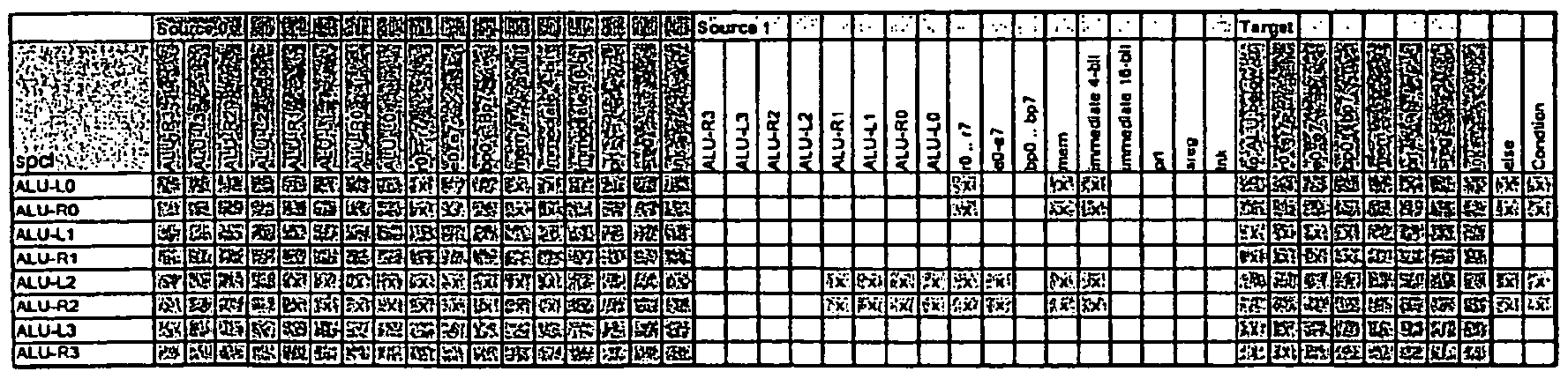

Table 9: Arithmetic, Logic and SFU ALU instructions
2.12.2.2 Move Instructions
These instructions move a source to a target.


Table 10: Move instructions
2.12.2.3 Load / Store Instructions
These instructions transfer data between the ALUs or register files to and from memory. The copy instruction allows to define the source and target in the memory. The address generator uses one ofthe base pointers (bpO ..bp7) and the offset as specified in the tables. Optionally, post-increment / decrement is possible with apO and apl .

m


Table 11: Memory Load / Store instructions
Push / Pop use bp7 /sp as stack pointer with post-decrement rsp pre-increment. Pop from stack loads the results directly to the registers i.e. without using the mem-out registers as with load/store operations.


Table 12: PUSH / POP instructions
2.12.2.4 Program Pointer Modifying Instructions
These instructions modify the program pointer implicitly. The SETLN opcodes are listed here, since they modify the PP indirectly with the next rfl instruction.


Table 13: Jump, Call, Call via Ink

Table 14: Link register load instructions Return is possible via stack, the Ink register or the interrupt Ink register


Table 15: Return from Subroutine and Ink '
2.12.2.5 Port read/write Instructions
These instructions read or write to ports. RDS and WRS transfer two bits ofthe status register from and to the ports.


m
m
w


Table 16: Port read/write instructions
.12.2.6 Miscellaneous Instructions
• hit stops the processor
■ inten enables the interrupts
• intdis disables interrupts.


Table 17: Miscellaneous instructions
2.12.3 Ambiguous Targets
Multiple ALUs may attempl to write within one cycle to the same target register. In this case the following list of priorities applies:

Table 18: register write priority
Only the object with the highest priority writes to the target. Write attempts of the other obji discarded.
2.13 Register Summary
The following section table summarize the registers in the FNC PAE.
General Purpose Register

Table 19: General purpose register file
Address Generator Registers

Table 20: AG Registers
2.13.3 Mem-in, Mem-out Register
The memory registers are use for transfer between the FNC-core and the memory. Reading from memory (!dw, ldbu, Idbs) load the result values to mem-out. The ALUs can access this register in the next cycle. Writing to the register is performed implicitly with the store instructions. The Ram is written in the next cycle.

Table 21: Mem Registers
2.13.4 Link and Intlnk Register
The Ink and intlnk register store program pointers. It is not possible to read the registers.

Table 22: Link Register
2.13.5 Status Register
Direct access to the status register is not possible, however conditional statements in the first ALU row use this register .

Table 23: Status Register Bits
2.13.6 Ports
The usage ofI/O ports is defined as follows

Table 24: Ports
2.14 SFUs
The FNC-PAE supports up to 16 SFUs, while each ofthem can execute up to 7 different defined SFU instructions. SFUs operate in parallel to the ALU data-path. Each instruction may contain up to two SFU commands. Each SFU command disables all or ar3 in the bottom row. The results ofthe SFU operation are fed into the bottom multiplexers, instead of the results ofthe disabled al3. SFU instructions are non- conditional and are executed whether the respective ALU path is active or not.
SFUs may access all registers as sources but no ALU outputs.
The SFU instruction format is shown in Table 25:

Table 25: SFU instruction format
The SFU may generate a 32-bit result (e.g. multiplication). In this case the result is written simultaneously to two adjacent registers, requiring the target register to be even. The least significant 16-bit word ofthe result is written to the even register, the most significant word is written to the odd register.
For each of the 16 SFUs Copro-instruction = 7 is reserved for multi-cycle SFUs. (see 2.14.1)
Copro# selects one of up to 16 SFUs. SFUs 0-7 are reserved for PACT standard releases.
2.14.1 Multi-cycle SFUs
Typically a SFU is required to process its operation within the timeslot (one cycle) determined by the ALU data-path. If the SFU requires multiple cycles (e.g. division), it has to support a valid flag identifying the availability of the result. Pipelined SFU operation is supported by issuing multiple SFU commands. Whenever the availability of a result is indicated by the valid flag and a new SFU command is issued, the result is written into the register file. All SFUs have to support the command "SFU Write Back" (CWB, CMD = 7) that writes available results into the register file.
2.14.2 SFU O
The SFU 0 provides signed and unsigned multiplication on 16 bit operands. The least significant word of the result is written to the specified target register. The most significant word is discarded.
The result is available in the target register in the next clock cycle.

Table 26: SFU 0 instructions
2.14.3 SFU 1
SFU 1 provides a special function to read and write blocks ofbits from a port. Bit-block input (ibit)
The SFU reads a 16-bit word from a port and shifts the specified number ofbits to the target (left-shift). If all bits have been "consumed", a new 16-bit word is read.
Bit-block output (obit)
The specified number of bits ofa source is left-shifted to the SFU. As soon as overall 16 bits have been shifted, the SFU writes the word to the output port.

Table 27: SFU 1 instructions
2.15 Memory Hierarchy
The FNC-PAE uses separate memories foT Data (D EM) and Code (1 E ). Different concepts are implemented:
• DMEM is a tightly coupled memory (TCM) under explicit control by the programmer
■ IMEM is implemented as 4-way associative cache which is transparent for the programmer.
The next hierarchy level outside ofthe F C-PAEs depends on the system implemention in a SoC. In this manual we assume reference design, which provides a good balance between area and performance.
The reference design consists ofa 4-way associative cache and interface to an external GGDR3 DRAM.
Several Function PAEs are mapped into a global 32-bit address space and share both interfaces. Access to the interfaces is arbitrated fairly.
Figure 18depicts the basic structure ofthe memory hierarchy spanning several Function PAEs, the shared D-cache and the shared Sysmem interface. The Instruction decoder accesses the local IRAM, which updates its content automatically according to its LRU access mechanism. The Load-Store unit may access the local TCM, the shared D-cache or the shared SYSMEM. The TCM must be updated under explicit control of the program either using the load /store Opcodes or the Block-Move Unit.
All data busses are 256 Bit wide. Thus a 256 Bit opcode can be transferred in one cycle or up to 8 x 16 bits (16-bit aligned) can be transferred using the block-move unit.
Note
The implementation of the D-cache and SYSMEM are out of scope for this
f. document. However the
! SYSMEM must be designed to support the highest possible bandwidth.
·; (e.g. by using burst transfers to external D AMs).
D-Cache Arbitration:
■ Highest priority has FNCO
■ FNCI to FNCn are using round robin
SYSlVIErvl Arbitration:
• Highesi priority has FNCO
■ FNCI to RNC3 have falling priority
■ FNC4 to FNCn use round-robin.
2.15.1.1 Bootstrap
Needstobedefined
2.15.1.2 ALU/ AM-PAE array (re-)configuration and FNC-PAE booting
Theblockmoveunitofone oftheFNC-PAEsmayboototherFNC-PAEs or(re-)configurethe arrayof ALl)-/RAM-PAEsbyfetchingcode or configuration data from theexternal memory.
Whileconfiguringanotherdevice,theWoclc-move unitis selectingthe targettobereconfiguredor booted, Simultaneously itisrising Iheconfigurationoutputsignal, indicating theconfiguration cycleto thetargetunit.
2.16 Integration into the XPP-array
TheFNC-PABwillbecormecled neartheRAM-PAEsoftheevenrowsofiheXPParray.The FNC- PAEswill haveports toexchangedatadirectlybetween theFNC-PABcoresorexternal components withouttheneedtogothrough the XPPamydatapaths.
2.17 Planned extensions
Some featuresarenotyetimplementedandsummarizedin thefollowingsections.
2.17.1 Shadow Register File
All instructionsmodifyingtheppcontain aSDW(shadow)bit,selectingtheregisterfiletobe used after thejump. IfSDH'issetto \, theshadowregister Aleis used. ForinstructionsretandInktheSDW-bitis restoredaccordingto thecallingsubroutine.
fl Usage ofshadow registers is not Implemented yet
2.17.2 Opcode Execution within Delay Slots
Someopcodescausedelay aloisbecauseofpipelinestageswhenaccessingmemories.HPCdoesnot generateadelayslotbutexecutes the targetinstructionin theverynextcycle. Thedelayslotcausedby LPCinlowperformance implementationsshouldnotbeusedforcompatibilityreasons. Thedelayslot causedbyfJMPOcannotbe usedforexecutionofotheropcodes.
jmp andcall(Assemblerstatement OH/)will leadtoonedelayslotwhich maybeusedbyanother opcode,retcausestwo delayslots.
Usingdelayslots foropcodeexecution-wheneverthetypeofapplication allows suchbehaviour- eliminatesperformancereduction whilejumping. Howeveroperationswhichmodifytheprogramorstack pointersare forbidden. Furthermore,during the first delayslotcausedbyRE no memoryaccessis possible.
0' The current Implementation does not allow the usage of delay slots
2.17.2.1 Jumps over Segments
The definition ofP C¾pcodes reserved bits for longjumps using up to four program segment pointers (psp). .
[j This feature ts planned as future extension.
2.17.3 Data Segment Pointer
The instruction format allows the definition of up to four data segment pointers. Selection ofsegments extends the addressable memory space.
Chapter 3
Assembler
The Function PAE is can be programmed in assembler language and - in a second project phase - in C. The FNC-Assembler supports all features which the hardware provides. Thus, optimised code for high performance applications can be written. The assembler language provides only a few elements which are easy to leam. The usage ofa standard C-preprocessoT allows the definition ofcommands preceded with the "#" symbol. Examples are ^include and conditional assembly with #i ... #endif.
The FNCDBG, which is an integrated assembler, simulator and debugger, allows simulating and testing the programs with cycle accuracy. The debugger shows all ALU outputs, the register files and the memory content. It features single stepping through the program and the definition ofbreakpoints.
General Assembler Elements
3.1.1 Opcode Syntax
The assembler uses a typical three-address code for most instructions: it is possible to define the target and two sources. Multiple ALU instructions are merged into one FNC opcode. The right ALU path is separated with '|' from the left ALU path. Each FNC opcode is terminated with keyword "NEXT.
The example Figun19 shows the structure ofone opcode. Ifa row ofALUs is not required it can be left open (the assembler automatically inserts NOPs here).
The example shows a typical opcode with branching to the right path with the OP1 condition.
t he column delimiter and the instructions for the right column can also-be written in the next code line. This may simplify editing and writing comments (see example chapter 3.6.4). If no column delimiter is defined, the assembler maps the instruction to the left columns (left path).
Ifno modification of the program pointer is required, the assembler sets the HPC automatically to point to the next opcode.
3.1.2 Comments
Comments are specified with
• ";" until end ofline.
■ "//" until end ofline.
■ /* comment */ nested comments arepossible.
3.1.3 Numbers, Constants and Aliases
Numbers can be
■ signed decimals
■ hexadecimal with syntax 0x0000
• binary with syntax ObOOOOOOOOOOOOOOOO
Constant definitions are preceded by keyword CONST. Constants expressions mustbe within parenthesis ( ).
Examples
CONST _linfi_oount = 96
CONST line_lengt = 144
CCM5T frame = rrax_line_count * line_lenght
CONST rracrcbl<xJc_lasC_elerenC = ((8 * 8) - 1)
CONST frame =
CONST MB_I4x4 = 0
Aliases arepreceded by keyword ALIAS
Examples
ALIAS state = r6
ALIAS ctx = m
ALIAS trnsTab = tp3
Object Naming, Default Aliases

Table 28: Assembler naming of objects and registers
Immediate valuesareprecededby The numberofallowed bitsoftheimmediatevaluedepends the ALU instruction.
J Refer to referTable 9 to Table 17 for the definition which Immediae
values areavailable for a specific instruction.
3.1.5 Labels
Labelsdefine addresses intheinstruction memoryandcanbedefinedeverywherein betweenthe opcodes. Labels aredelimitedbyacolon ":".TheinstructionsJMPL, JMPS, HPC,LPCand CALLTefer tolabels. Furthermore,DatamemorysectionscanbenamedusingLabels. Forthe Datasection, (be assemblerassigns theByte-address totheLabel, forprogrammemory >> assignstheabsoluteentry(226- bitopcodeword). Refertosection 3.5 forthedefinitionofreservedlabelsforresetandinterrupt
Optionallytheregistersettobe usedwhenjumpingtoa label can bespecifierwith(RSO)rsp. (RSI) beforethecolon.
3.1.6 Memory
Instruction RAM
The Instruction RAM is initializedwiththekeywordFNC_IRAM(0).Theparameter(here0)defines the F C-PAEcore towhich theinstructionmemory sectionisassigned.FNCJRAM(O)mustbespecified onlyifanotherRAMsection isdefined(defaultisPNCJRAM0)).
Data RAM
DataRAM sectionsarespecifiedwith the keywordFNC_DRAM(0).Theparameter(here0)defines the FNC-PAEcoretowhichthedatamemorysectionisassigned.
ParametersordatastructurescanbenamedusingLabels. Thelengthofthesectionmustbespecifiedif thedataisnot initalizcd:
R7W3ECTICM: 0¥IE[length! ?
0T
RTMSEEnCHi VKHDtlengh] ?
The symbol specifiesunrnitalizeddata.Lengthis thenumberofbyteaorwords,respectively. Word reservestwobyteswithbigendian byteordering1. TheMSB isaddressedwithaddressbit0=0,i.e. storedattheloweststorage address.
Datasectionscan alsobeinitialised usingalist ofvalues.
RAMSBnEN: ΒΪΤΒ lise of values*'
1 Currentybig endian Is supported. It is planned to allow also little endian mode. Then, FNCDBG will display Inltalized'words with reversed byte ordering within the words.
1 XDSDBS from Oct.Z6, 2005 requires the # symbol before numbers.
The values are separated by space characters. The first value is loaded to the lowest address.
The data sections are reserved in the Data RAM in the order oftheir definition. The Labels can be used in programs to point to the RAM section.
Example:
.

Note:
FNCDBG fills uninitialized Data RAM sections with default values:
• Oxfefe: reserved data sections
• Oxdede: free RA
FNCDBG shows the memory content in a separate frame on the right side. Bytes or words which have been changed in the previous cycle(s) are highlighted red. Figure 20
3.1.7 Conditional Operation
Arithmetic and move ALU instructions can be prefixed with one of the conditions. For restrictions on which ALU-instructions conditions can be specified, refer to Table 9 to Table 17 Column "Condition".
The status flags of ALU are available for evaluation for the ALU of the same column the row below. If the condition is TRUE, the subsequent ALUs that column are enabled. Ifthe condition is false, the ALU with the condition statement and all subsequent ALUs ofthat column don't write results to the specified source1.
The status of the ALUs of the bottom column (al3, ar3) are written to the status register for evaluation by the ALUs in the first row during the next opcode.
The conditions OPI (opposite column inactive) and OPA (opposite column active) are used to disable an active column based on the activity status ofthe opposite column. With ACT, a disabled column can be enabled again.
The LCL (last column active left) rsp. LCR (last column active right) are used as conditions which reflect the status ofthe final row of ALUs ofthe previous opcode.
The conditions are derived from three ALU flags:
• ZE: result was zero
■ CY: carry
■ OV: result with overflow.
1 Anyhow, the disabled ALUs provide results at their outputs which can be used by other ALUs

Table 29: Conditions
3.1.8 Program Flow
The FNC-PAE does not have a program counter in the classical sense, instead, a program pointer must point to the next opcode. The assembler allows to set the three opcode fields HPC, LPC and IJMPO which define the next opcode. The maximum branch distance for this type of branches is +-31.
The assembler instructions must be defined in a separate source code line.
3.1,8.1 EXIT branch
The instructions HPC, LPC and JMPS define (he next opcode when exiting a column. HPC, LPC or JMPS can only be specified once per column. The relative pointer must be within the range+-15. For branchesoutside of this range, JMPL must be used.
Syntax
» Default: without specification ofHPC, LPC orJMPS, the HPC field points to thepp+\ .
HPC HPCpointstothepp+\
HPC label HPCpoints tothelabel
KPC jfconst HPC points co ce fptcona
LPC LPCpointsto thep+1
LPC label LPC points to the label.
IPC flccnst LPC pcdncs to che fpwxnst
OMBfl JMPS points tothepp+l
JMPS label JMPSpointsto thelabel
OMPB Sccnst -MPs points Co the fjxmst
Fordefinition ofthe pointers, the assembler uses the followingscheme:
» The specification ofELSEbranches (see 3.1.8.2) has priority. The specified pointers are filled with those settings.
■ Then, the definitions as specified in the assembler code are filled into the not used pointers. • Ifnothingis specified in column, HPC is used ifnot already filled in, else LPC or, ifLPCwas already filled in JMPS.
The following tables (Table 30,Table 31) specify which pointers the assembler enters(during design- time) andwhich pointers are usedbased on the runtime activity ofcolumns. "Default" means, diet the exitpointer was not explicitly specified in the assemblercode.
Settings for the right columns are only applied where when the left column is inactive and theright columnsis active.
jj Note:
I Refer to 3.1.8.2 for the behavior with ELSE branches. If an ECSE branch
jj Is applied, the exit settings are overridden. Also lone jumps (JMPL)
i override the Exit settings.

runtime Note
m
§ V o a
a.
I a. 2
m
mm
m mm
m If right LPC = default, then HPC = 1 is used. m m m HPC = left target, both targets must be equal m mm
m
mm LPC = left target, both targets must be eqal m mm
M
mm
1H JMPS = left target, both targets must be equal

Table 30: EXIT behaviour (1)

Table 31: EXIT behaviour (2)
3.1.8.2 ELSE branch
Some ALU instructions allow the definition of "ELSE" branches. The ELSE branch evaluates the result of a conditional ALU instruction and defines one ofthe HPC, LPC or JMPS fields to point to the next opcode as specified by the target or default (ifno.target is specified). For restrictions, which ALU- instructions ELSE allow branches/refer to Table 9 to Table 17 Column "ELSE".
If the condition is TRUE, the ALU column is enabled and the setting for the EXIT branch is used. If the condition is FALSE, the ALU column is disabled and the setting for the ELSE branch is used. If an ALU column is disabled by a previous condition, the ELSE branch is not evaluated.
In case that more than one ELSE branches are defined in an opcode, the bottom specification is used.
? A long jump (J PL) overrides the ELSE branches if both are active.
Syntax:
The Else statements as defined below must be written in the same instruction line.
■ ! m label : use HPC in case that the condition in the previous instruction was FALSE.
■ ! LPC label : use LPC in case that the condition in the previous instruction was FALSE.
■ ! OMPS label : use IJ PO in case that the condition in the previous instruction was FALSE.
Table 32 shows which pointer is used based on the else statement. Ifthe condition in the line is TRUE, the specification ofthe EXIT branch is used (See Table 30, Table 31 ), If the condition is FALSE the else target (e) is used.


Table 32: ELSE behaviour
3.1.8.3 Long Jump
Long Jumps are performed by ALU instructionsjmp, which add an immediate value or another source to the program pointer If a long jump instruction is executed, the HPC LPC or 1JMP0 fields are ignored.
Syntax:
■ JMRL source : use a register or ALU or 6-bit immediate as relative jump target to the actual program pointer. The source is added to the pp.
■ JMPL ttconst : use an immediate value as relative jump target. The constant value is added to the pp.
Note:
3 Only one JMPL instruction per opcode is allowed
Assembler Instructions
The assembler uses in most cases the ALU instructions. However, some of the hardware instructions are merged (e.g. mov. movr, movai to NOV) in order to simplify programming. Besides the ALU instructions, a set ofinstructions allow to control the program flow on opcode level (e.g. definition of the HPC to point to the next opcode - see previous chapter).
Placeholders for objects:
■ target: the target object to which the result is written. Target "-" means that nothing is written to a register file, however, the ALU output is available.
■ src: the source operand, can also be a 4 bit or 6 bit immediate
■ srcO: the left side source operand, can also be a 4 bit or 6 bit immediate
■ srcI : the right side ALU operand, can also be a 4 bit or 6 bit immediate
■ const: 16 bit immediate value
■ bpreg: one of the base registers of the AGREG
" port: one ofthe I/O ports
Not all ALU instructions can be used on all ALUs. For restrictions refer to
Table 9 to Table 17.

Table 33: Assembler ALU instructions (1)
Note: movai (MOV -, tiCONST) moves an immediate 16-bit value to the ALU output which can be used by the subsequent ALU stages.

Table 34: Assembler ALU instructions (2)

Table 35: Assembler opcode instructions

Table 36: Assembler SFU 0 instructions

Table 37: Assembler SFU 1 instructions
3.3 Shadow Registers
The shadow register set is selected by one of ther following methods:
• RSO (standard register set) specified behind instructions CALL, JMPL or when the Ink register is set selects register set I . Example can, RSO labeli selects the standard register set. RETreverts to the register set of the calling routine.
■ RSI (shadow register set) specified behind instructions CALL, JMPL or when the Ink register is set selects register set I . Example can, RSL labeli selects the standard register set. RETreverts to the register set of the calling routine.
• The register set can also be specified in label with syntax label(RSO): or label(RSl):. Any MOV or ADD to Ink register, CALL or JMPL using that label will switch to the register set as specified with the label. RET reverts to the register set ofthe calling routine.
The (RSO) rsp. (RSI) definition HPC LPC or JMPS point tp the label However with HPC Ink. LPC Ink, JMPS Ink the register set is selected.
3.4 Input/ Output
Stimuli can be defined in a file and can be read with using an FNC-PAE I/O port. Vice Versa, data can be written via a port to a file.
Currently only input and output port 0 is supported.
The files must be specified using the command line switches
■ -inX <file>, X specified the part number (currently 0)
■ -cutx <file>, X specifies the part number (currently 0)
Similarly the SFU instructions IBITreads input bitfields from a file. OBITwrites bitfields to a file. The files must be specified using the command line switches
• -ibit <file>
■ -obit <file>
The numbers in the stimuli files must fit into 16 bit and must be separated with white-space characters. Decimal and hexadecimal (0x0000) figures can be specified.
Reset and Interrupt Vectors
The assembler generates the default module "FNC DISPATCHER" defining the reset and interrupt vectors which are loaded to the program memory at address 0x0000. It consists of a list oflong jumps to the entr oints ofthe reset and u to seven interrupt service routines.

The assembler inserts the branch addresses to the reserved respective labels as defined in Table 38.

Table 38: Reserved Labels
The FNC RESET: label is mandatory, the entry points of ISR routines are optional.
After calling the interrupt routine (ISR), further interrupts are disabled. The ISR must enable further interrupts with the El instruction, either for nested interrupts or before executing RETI.
§ Notes
The ISR must explicitly save and restore all registers which are modified,
fj either using the stack or by other means.
Interrupt requests are only accepted in opcodes using the HPC. Thus,
opcodes which are using the LPC or J PS cannot be interrupted.
Therefore loops should always use the HPC and the LPC when exiting.
3.6 Examples
The following examples demonstrate basic features of the Function PAE. We don't define aliases in the examples in order to demonstrate the hardware features of the architecture'.
3.6.1 Example 1
1 The examples are only intended to show the FNC-PAE features, some examples can be optimised or written differently, but this is not the scope of the examples.
The example shows basic parallel operation without conditions.
The contents of rl ..r5 and eO .. e2 are accumulated with result in rO. The first opcode loads the registers with constants. The second opcode accumulates the registers and writes the results to rO.
Since EREGSs cannot be used as sources in row 0, rl .. r4 are added in the first row.
Exanple 1
The values in rl.. rS and eo .. e2 are accumulated with result written to rO.
Note ERB3S cannot be used as sources in row O
;load test values
MOV rl. #1 I MOV r2, «2
MOV el, «7 I MOV e2, 88
MOV r3, «3 I MOV eO, #6
MOV r4, #4 I MOV r5, #5
NEXT
; Aceunulate all
AO) -,rl,r2 | ACD -,r3,r4
ADD -.alO.arO | ACD -,rS,eO
ADD -,all,arl j ADD -,el,e2
ADD r0,al2,ar2 | NOP
NEXT
HAW MOT
3.6.2 Example2
The example shows how conditions on instruction level (i.e. within an opcode) can be used.
The example delimits the value in register rO to lower and upper boundaries which are defined i r2, respectively. Then, the result is multiplied by 64 with shift left by 6 bits.
Figure 21
This operation requires two comparisons and decisions as depicted in igure 7.
First, rO is compared against the upper limit r2. For this, we subtract r2- rO. If the result is greater /equal 0 (i.e. rO >= upper limit) column L is disabled and Column enabled by means of the OPI condition. Then
the right path moves the r2 (upper limit) to rO.
The second comparison must also be done in the left path. We subtract rl from rO. Ifthe result is greater/equal = (i.e. rO < = lower limit), rl is moved to rO. Otherwise, the right path is enabled and no further operation is performed. Figure22>hows the behaviour during runtime. The shaded ALUs are enabled while "-" means, that those ALUs are disabled.
The code demonstrates this behaviour with three different values for rO. The NOP opcodes which are explicitly defined in assembler source can be omitted. If OPs are not defined in a row, the assembler will insert them automatically. In the example, the second OP1 Is not required, since NOPs don't need to be activated since they are doing nothing. We used the NOPs just to demonstrate the general principle.
******

(
G

3.6.3 Example 3
The exampleshows how conditions on instruction level (i.e. within an opcode) can be used and how a loop can be defined by conditional specification ofthe HPC respectively. Furthermore it demonstrates the compactness ofFNC-PAE Code.
The example multiplies sequentially two 8 bitnumbers in rOand rl with result in r2. The loop-counter is r7. which is decremented until 0. Ifthe loop counter is not 0, the ! HPC loop ("ELSE HPC loop") statement specifies to use the HPCentry ofthe opcode for the loop target address. Iftheresult ofthe SUB which decrements the loop-counterwas not zero, the HPC points to the label "loop"'. Otherwise (after the loop) the LPCentry ofthe opcode points to the next opcode. The assembler loads the HPCand IPCbits accordingly- the LPC must not be defined explicitlyifthe branch points to the next opcode.
The ACTconditional statement is required toreactivate the left column in order to process the loop- counter in those cases when azero was shifted into carry. Thus, only the ADD instruction is omitted. )

1 The assembler uses the absolute value of HPC. On the physical side, the generated 6 bits of the HPC pointer are relative to the current PP.
HALT
NEXT
3.6.4 Examples 4
The examples show how to access the data memory, the visualisation in F CDBG and the behaviour of the auto-incrementing address pointers apO and apl . The examples shows also that the "|" delimiter can be used in the next line. This simplifies commenting left and right columns separately.
Task
In a first loop the data memory is alternatively loaded with 0x1111 and 0x2222 (initloop).
The second loop (modifyloop) first reads the content ofmemory, compares the content with 0x1111. In case that 0x1111 is read, 0x9999 is added (result Oxaaaa), else the low byte are is set to 0x00.
Implementation 4a
The example 4a implementation defines the memory sections as bytes. The debugger shows the bytes in a memory line in increasing order with the smallest byte address at the left.
Initloop:
The base register bpO points to DemoRamO. The address generator uses bpO as base address and adds the offset r3 to build the memory address. Writing to memory uses the byte store STB, thus r3 must be incremented by 1. The offset address bit 1 ofr3 is checked and the value to be written in the next loop is moved to r0.
Modifyloop:
Reading from memory is done with Word access and requires two steps. The result ofthe LDW instruction is available one cycle later in the mem register. Therefore we must launch one LDW before the loop in order to have the first result available in mem during the first loop. The apO read pointer and apl write pointers are explicitly incremented by 2. The compare operation is performed in the first opcode, the result is written in the second opcode in the loop.
. ,- Exanple 4a
' initalize ram "demo" o .. QxlO with Qxllll and 0x2222.
; add 0x9999 to Oxllll values, and replace
; the LSB of 0x2222 by 0x00.
,- The RAM is defined as bytes.
; the pointers are incremented explicitly
FNC_RESET:
FNC_DAM(0)
DemoRanO: BVTE[0x20] ?
DenoRaml: EKTE[2] ?
EhdOfRam:
FNC_IRBM(0)
;init RAM
VCN xl, 80x1111 I VCN r2, #0x2222
VCN bpO.ttDerroRarTC j VCN rO, #0x1111
VCN r3,H0
VCN r7,#0xl0
NEXT
loop handling in first row

Implementation 4b
The example 4b implementation defines the memory sections as words. The debugger shows the words in a memory line in increasing order with the smallest word address at the left. Since we use little endian mode, the debugger shows the LSB in a word correctly aligned at the right.
Initloop:
The memory is loaded using byte accesses. The address bits ofapO are checked and the decisions whether 22 or 11 should be used in the nexts cycle depends on the address bits. We use the postincrement mode of apO. Since LDB is used, apO increments by 1. Since the incremented value ofapO is
not available during the current cycle, apO is read and one is added value before the bit 1 is checked (AND with 0 10). When stepping through the loop one can see that the LSB of each word is written first.
Modifyloop:
Reading from memory is done similarly to example 4a using with Word accesses. However the postincrement mode of the apO read pointer and apl write pointers is used. Since we use LDWrsp. STW, the pointers are incremented by 2.
***********-**************-******■*■-****+*********+***-************+**
; Exarrple 4b
initialize ram "demo" 0 .. 0x10 with 0x1111 and 0x2222.
; add sQx9999 to Oxllll values, and replaces
; Che LSB of 0x2222 by OxOO.
; the RAM is defined as words.
,· Che pointers are incremented using auto increment.

trodifylocp:
LDW bpO + (apO++) ; : read word far next leap
I MV -,irem ; R: gee rem-read result from previous cycle
CMP arO, 80x1111 ; L: carpare
HQ AED rO,arO,rl L: if EQ: add
I OPI AND rO,arO,r2 ; R: if notEQ: trask
NEXT
STW bpO + (apl++),rO ; L: write rO
I NOP ; R:
NOP L:
SUB r7,r7,ttl ; L: deer, loop-counter
I NOP ; R:
ZE NOP ! HPC nodifylcop ; l>: if zero, exit via LPC = next Opcode
; L: else use HPC = modifylccp
I NOP ; R:
NEXT
HALT NEXT
3.6.5 Examples 5
The following examples demonstrate the usage of the branches using the HPC, LPC or IJ P0 pointers. For demonstration of branchnes, a loop increments rO which is compared to a constant value. In example 5a, the full assembler code is shown. Examples 5b to 5d show only the opcode which controls the branch.
; Example 5: Branching and Junps
Branching is controlled by rO which is increcrented.
; a.) EXIT branch via HPC and LPC.
MOV rO, #0
NEXT
loop:
; branch statement:
CMP rO,#0 I NOP
BQ NOP I OPI NOP
HPC destO I LPC destl
NEXT
; branch targets:
dest_next:
MOV rl,(t0xffff
HPC lccpend
NEXT
destO:
MOV rl.ftO ; dunny
HPC loopend
NEXT
destl:
M3V rl,81
HPC lccpend
NEXT
dest2:
MOV rl,»2
NEXT
endless loco
loopend:
ADD rO.rO.Hl
JMPL loop
NEXT
HALT NEXT
Exampe 5a
shows a two target branch using the HPC and LPC assembler statements for the left and right path. Only the HPC rsp. LPC statement of the active path is used for the branch. LPC requires an additional cycle since the current implementation has only one instruction memory. The instruction at label Inopend uses JMPL loop ALU instruction, which allows a 16-bit widejump. In this example, also an unconditional HPC loop would be possible.
Hardware background
The assembler sets the pointers HPC to destO, LPC to destl. Furthermore, it sets the opcode's EX1T-L field to select the HPC-pointer if the left path is enabled and the EX1T-R field to select LPC-pointer if the right path is enabled during exit.
Exampe 5b
shows a two target branch using an ELSE branch and the exit ofthe left path using the LPC. If the comparison is equal the left path is activated and the LPC destO statement is evaluated i.e. the branch goes to destO. Else, the ! HPC destl is used and the jump target is destl .
Hardware background
The assembler sets the pointers HPC to destl, LPC to destO, further the opcode's EXIT-L field to select the LPC. Ifthe condition was TRUE, the EXIT-L field selects LPC as pointer to the next opcode, since the left path is enabled. If the condition was NOT TRUE, the ELSE bits ofthe ALU instruction select the HPC-pointer.
Note:
If the LPC desto statement would be omitted, the assembler would set the LPC per default to point to the next opcode (label destjiext).
CMP ro.flo I NOP
EQ NOP
! HPC destl
LPC destO
NEXT
Exampe 5c
shows a three target branch using an EXIT branches and an ELSE branch. The first comparison enables the left path ifrO >=2, thus LPC dest2 is evaluated and the LPC pointer is used. Otherwise the right path is activated. The second comparison (ALU arJ) enables the right path ifrO = 1, thus JMPS destl is evaluated and the pointer IJMPO is used. Otherwise the ! HPC desto is evaluated and the branch goes to destO using the HPC pointer.
Hardware background
The assembler sets the pointers HPC to destO, LPC to dest2 and IJMPO to destl . The EXIT-L field specifies to use the LPC if the left path is active. The EXIT-R field specifies to use the IJMP1 if the right
path is active. The ELSE bits of the NOP instruction for ALU arl define to use the HPC ifthe condition is NOT TRUE.
During runtime the hardware must decide which pointer to use. First the else bits are checked ifthe condition is NOT TRUE. Otherwise, the enabled path selects the pointer using EXIT-L or EXIT-R, respectively.
Note: if both paths would be enabled, the priority HPC - LPC - IJMPO (lowest) would be applied.
CMP rO,fl2
NOP I OPI CMP rO,#l
LPC desC2
NOP I HQ NOP
I ! HPC destO
I JMPS destl
NEXT
3.6.6 Example 6
The example shows how to read and write from files. Two types ofports exist: the general purpose streaming ports and special ports for the 75/7"and OBITSFV instructions. Both types are show in the following example. The files are specified with the following command line:
xfncdbg -inO infile.dat -outO c tf le.dat -ibit ibitfile.dat -obit obitfile.dat exa6.fnc the stimuli files are defined as follows:

The first loop reads eight values from the file, adds 10 and writes the result back to the outfile.dat.
The second loop shows how the ibit function can be used to extract bitfields and how to read in sequentially a variable number of bits.
The input bitstream is packed into consecutive 16 bit words, with the first bit right aligned at the MSB. The first 4 bits of the bit-stream are a command which defines how many subsequent bits must be read. Command word = 0 stops the loop. SrcO of the ibit instruction is always set to #0. Figure23shows the sequence ofthe sample ibitfile.dat. In the example the extracted bits are accumulated.
Usage of I/O and ibit
; loopl:
; reads data frcrn file adds 0x10
; and writes the result back to a file
; α-nrrand line option -ino infile.dat -cutO outfile.dat
; lcop2:
; the second loop reads bit fields via SFU ibit from a file
; comrand line option -ibit ibitfile.dat -obit obitfile.dat
FNC_RESET:
MOV r7, #8 ; lcopoounter
MOV rl, 80x10 ; to be added
NEXT
lcopl:
VN -, pO ; read port.
ADD r2,al0,rl
NEXT
K3V p0,r2 ; write port
SUB r7,r7,#l ; dec.counter
ZE NOP ! UPC lcopl
NEXT lcop2 reads a structured bit-stream
the bit stream is structured as follows:
4 bits carmand define how trany subsequent bits must be read in.
the read bits are aocunulated in r2
the loop is inalized when command = 0 is detected.
MOV rO, 80
MOV rl. 80
NOV r2, #0 ,- accu init
MOV r3. #4 ; number of c mand bits
NEXT
ADD r2, r2,rl ,- accumulate bits
NOP
NOP
IBIT r0,«0.r3 ; read 4 cumund bits
NEXT
CMP rO, 80 ; was comand <= 0 ?
NOP ! LPC loop2end ; break loop if carmand = 0
NOP
IBIT rl,80,r0 ; read bits, number as specified by previous 4bits
HFC loop2
NEXT
loop2end:
HALT NEXT
3.6.7 Example 7
The example shows the usage of the Stack and subroutine call and return. The calling routine is a loop which increments a pointer to a RAM . Dataram which is passed to the subroutine.
The subroutine picks the pointer from the stack after having registers saved. It calculates the average value of 8 consecutive words and writes the result back to the stack at the same position where the pointer was passed. The subroutine saves all registers which are affected to the stack and recovers them before return. Generally spoken, there is no difference to classical microprocessor designs.
A Note
Ij Subroutines have in most cases some overhead for stack handling and
(i saving registers. Therefore usage of subroutines in inner loops of time- critical algorithms should be carefully evaluated. A faster possibility is the
j usage of the link register Ink, however Ink can only be used once at the
j; same time.
Table 39 shows the stack usage of this example.

Table 39: Stack usage of example 7
; Call, Recum
; the calling routine pushes a pointer onto the stack.
; the subroutine calculates the mean value of a 8 values of the specified memory section ; and pops the resulting value onto the stack. The subroutine also restores changed register ■ values before returning.
FNC_RESE :
!*CJ3RfiM(0)
Dataram:
WORD 01234 5S 7
WORD 891011
Results:
WORD [41 ?
Stack:
WOED (20) ?
TcpOfStack:
FNC_n»M(0)
MDV -, fttfcpOfStack
MOV sp, alO ; defne stack pointer
I MOV bpO,#Results
M3V rO, ttDataram ; initial pointer to data.
M3V r7, «4 ; loop counter
NEXT
lcopl:
FUSH rO push pointer to stack
NEXT
CALL awa ,-puts return address to
NEXT
POP rl pep result from stack
NEXT
STW bpO + rO, rl Store result
SUB r7,r7,t(l dec.loop counter
ZE NOP ! HPC locpl
ACT ADD rO.rO, 82 increment data pointer (for next loop)
NEXT
HALT NEXT
—subroutine awa
pops the pointer from stack, calculates the average value of the B data values. pushes the result to stack and returns.
uses rO, r7,ap0, bpO therefore those registers are saved.
awa:
; save regs
PUSH rO save register of calling routine
NEXT PUSH r7 save register of calling routine
NEXT NOP NOP, since AGregs cannot be accessed in rowO
PUSH apO save register of calling routine
NEXT NOP
PUSH bpO save register of calling routine
NEXT
; extract data from stack
; note : imrediate agreg offsets and negative offset mist be clarified
NOP
ADD sp, sp,#10 ; go up 5 stack entries for parameter
MDV r0,#0
NEXT NOP
LEW sp + rO read stack,
HW apO,#0 clear apO
NEXT
NOP
NEW bpO.rrem pointer
NEXT
; processing loop
LOW bpO + (apO++) ; read first value
M0Vr7,#8 loop counter
NEXT
awalccp:
ADD rO,rO,mem accumulate
LOW bpO + (apO++) read for next loop
SUB r7,r7,#l dec.counter
ZE NOP ! HPC awaloop;
NEXT
SHRS rO,rO,#3 divide by 8
MOV r7,S0 offset for storing to stack
NEXT
STW sp♦ r7,r0 stare result to stack
SUB sp,sp,#10 restore
NEXT
restore registers and return NOP
POP bpO
NEXT
NOP
POP apO
NEXT POP r7
NEXT POP rO
NEXT RET NEXT
-- end of subroutine
Appendix A
FNC Debug Beta (Oct.28, 2005) Figure 24
The following picture shows a commented view of the current status ofthe F CDBG.EXE.
The debugger is invoked by command line with the initial file. A C-preprocessor must be installed on the system.
The frame ofthe previously executed opcode shows:
• green: processed instructions
• red: disabled ALU instructions. The result is available at the ALU outputs anyway.
■ — : NOPs
The breakpoint can be toggled with right mouse click over the opcode.
The following attachment 2 does form part of the present application to -be relied upon for the purpose of disclosure and to be published as integrated part of the application.
Attachment 2
Introduction
IS-95 uses two PN generators to spread the signal poweruniformly over the physical bandwidth ofabout 1.25 MHz. The PN spreading on the reverse linkalso provides near-orthogonality ofand; hence, minimal interference between, signals from each mobile. This allows universal reuse ofthe band offrequencies available, which is a major advantage ofCDMA and facilitates soft and softer handoffs.
A Pseudo-randomNoise (PN) sequence is a sequence ofbinary numbers, e.g. ±1, which appears to be random; but is in fact perfectly deterministic. The sequence appears to be random in the sense that the binary values and groups or runs ofthe same binary value occur in the sequence in the same proportion theywould ifthe sequence were being generated based on a fair "coin tossing" experiment. In the experiment, each head couldresult in one binary value and a tail the other value. The PN sequence appears to have been generated from such an experiment. A software or hardware device designed to produce a PN sequence is called a PN generator.
A PN generator is typically made ofN cascaded flip-flop_circuits and a speciallyselected feedback arrangement as shown in Figure 25 ~
The flip-flop circuits when used in this way is called a shift register since each clock pulse applied to the flip- flops causes the contents ofeach flip-flop to be shifted to the right.The feedbackconnections provide the inputto the left-most flip-flop. WithN binary stages, the largest number ofdifferentpatterns the shiftregister can have is 2N. However, the all-binary-zero state is not allowed because it would cause all remaining states ofthe shift registerand its outputs to be binary zero. The all-binary-ones state does not cause a similar pro¬ blemofrepeated binary ones provided the number offlip-flops input to the module 2 adder is even. The period ofthe PN sequence is therefore 2N-1, but IS-95 introduces an extra binary zero to achieve a period of 2N, where N equals 15.
Starting with the register in state 001 as shown, the next 7 states are 100, 010, 101, 110, 111, 011, and then 001 again and the states continue to repeat. The output taken from the right-most flip-flop is 1001011 and then repeats. With the three stage shift registershown, the period is 23-1 or 7.
The PN sequence in general has 2N/2 binary ones and (2N/2]-l binaryzeros. As an example, note that the PN sequence 1001011 ofperiod 23-1 contains 4 binary ones and 3 binaryzeros. Furthermore, the number of times the binary ones and zeros repeat in groups or runs also appear in the same proportion they would ifthe PN sequence were actually generated by a coin tossing experiment.
The flip-flops which should be tapped-offand fed into the module 2 adder are determined by an advanced algebra which has identified certain binary polynomials called primitive irreducible or unfactorable polyno¬ mials. Such polynomials are used to specify the feedback taps. For example, IS-95 specifies the in-phase PN generator shall be built based on the characteristic polynomial
PI(x) = xl5+xl3 + x9 + x8 + x7 + x5 + 1 (1)
Now visualize a 15 stage shift register with the right-most stage numbered zero and the successive stages to the leftnumbered 1, 2, 3 etc., until the left-most stage is numbered 1. Then the exponents less than 15 in Eq. (1) tell us that stages 0, 5, 7, 8, 9, and 13 should be tapped and summed in a module 2 adder. The outputof the adder is then inputto the left-most stage. The shiftregister PN sequence generator is shown in Figure26
PN spreading is the use ofa PN sequence to distribute or spread the power ofa signal over a bandwidth which is much greater than the bandwidth ofthe signal itself. PN despreading is the process oftasking a signal in its wide PN spread bandwidth and reconstituling it in its own much narrower bandwidth.
NOTE: PN sequences can be used in at least two ways to spread the signal power over a wide bandwidth. One is called Frequency Hopping (FH) in which the center frequency ofa narrowband signal is shifted pseu- do randomly using the PN code. A second method is called Direct Sequence (DS). In DS the signal power is spread over a widebandwidth by in effect multiplyingthe narrow-band signal by a wideband PN sequence. When a wideband signal and a narrowband signal are multiplied together, the resulting product signal has a bandwidth aboutequal to the bandwidth ofthe wideband signal.
IS-95 uses DS PN spreading to achieve several signaling advantages. These advantages include increasing the bandwidth so moreuserscan be accommodated, creating near-orthogonal segments ofPN sequences which provide multiple access separation on the reverse link and universal frequency reuse, increasing tolerance to interference, and allowing the multi-path tobe resolved and constructivelycombinedbythe RAKE receivers. Multipath can be resolved and constructively combined only when the multi-path delaybetween multipath component signals is greater than the reciprocal ofthe signal bandwidth. Spreading, and thus in- creasing the signal band-width, allows resolution ofsignals with relativelysmall delay differences.
Assume a signal s(t) has a symbol rate of 19,200 symsec. Then each symbol has a duration of1/19200 or 52.0833 μsec. Ifs(t)is module 2 added to a PN sequence PN(t) with chips changing at a rate of 1.2288 Mchips/sec, each symbol will contain 1.2288x52.0833 or exactly 64 PN chips. Theband-width ofthe signal is increased by a factorof64 to 64x1 ,200 or 1.2288 MHz. The received spread signal has the form PN(t- t)s(t-t). At the receiver, a replica ofthe PN generator used at the transmitter produces the sequence PN(t-x) and forms the product . When the variable x is adjusted to equal t, PN(t-x)PN(t-t)s(t-t) equals PN(t-t)2s(t-t) which equals the desired symbol stream s(t-t) since PN(t-t)2 always equals one. This illustrates despreading.
Typical PN code length
In IS-95 two different type ofPN sequences are used:

PAE Bit Logic Extension
XPP-llI PAEs support one line oflogic elements within thedata path. Up to three registers can feed data into the Bit-Logic-Line (BLL), the results can be store in up to two registers.
A single Bit-Logic elementcomprises a three input, two output look-up table (LUT). figure27
To achieve high siliconefficiencyeach bit inthe BLL is processed in the same manner, which means only one set ofmemory is needed for the whole line ofLUTs.
Figure 28 shows the configuration ofa BLL asused forPN Generators;
A PAE stores up to 4 BLL configuration, which are accessible using the commands bll, bl2,bl3, bl4 similar to an opcode.
Figure 29 shows the arrangement ofbit level extensions (BLE) in aXPP20 processor. The side ALU- PAEs nextto the memory PAEs offer the BLL extension. For area efficiency reasons thecoreALU-PAEs does nothave the extension implemented.
PN Generator Implementation
Within eachLUT a modulo 2 adderis configured. Sinceeach LUT looks the same, in addition a multiplexer is implemented inthe LUT to bypass the adder, according to theusedpolynomial.
Figure 30 sJ» e the schematics ofa LUTand the according configuration data:
QOo is fed to the flag registerFU3, which is used to store a generatedbit and distribute it tothe consuming algorithms over the event network.
InregisterROthePN datafastored,registerRl containspwhichdefinesth pol nomial »« O eup infr* examplebelowbysettingthemultiplexerineachLUT. ( Figure 31>
Multiplesequentialiterationsgenerate thePNsequence: igure 32
This verybasic method generates PN sequences up to the word length oftheALU.
Long PN sequences
For longer sequences (i.e. IS-95 Long PN Code is'24Z), the generation has to be split intomultiple parts. Since XPP-III is planed for Software Defined Radio application having 24-bit wide ALUs, two processing steps are necessary to compute a42-bit long PN sequence. Figure 33
The first step computes the lower halfofthe PN sequence. The Carry flag (C) is usedto move the lowest bit ofthe higher halfofthe sequence into the shifter. FV3 is used to carry the sum ofthe modulo 2 adders to the processing ofthe higher half. Figure 34
Higher halfprocessing moves the lowest bit into the Carry flag (C) and uses the FV3 flag as carry input for the modulo 2 adder chain.
As a prerequisite the shown operation need to preload the Carry flag before the processing loop starts.
An example algorithm is given below. rO, rl, r2, r3 are preset as constants by configuration. rO and rl contain the base values for the PN generation, r2 and r3 containpolynomial definition for the higherrespective lower part ofthe PN processing. Since rl is shifted right and therefore destroyed it is reloaded right after from the configuration memory.
l

The code requires 7 entries in the configuration memory.
What is described in the preceding text is inter alia a data processing device comprising a multidimensional array of ALUs, having at least two dimensions where the number of ALUs in the dimension is greater or equal to 2, adapted to process data without register caused latency between at least some of the ALUs in the corresponding array.
Furthermore, it is suggested that at least one ALU-chain is provided without registers between ALU-stages of the chain and/or that signals are provided between ALUs in different pipelines referring to states and/or conditions in the other pipeline and/or that at least one ALU, preferably an ALU in a pipeline, preferably each ALU in a pipeline and preferably each ALU in each pipeline, is provided that is capable of evaluating a condition and carrying out an operation in response thereto and/or to not carrying out an operation in response thereto, the evaluation and execution or non-execution of operations in response thereto taking place preferably in one clock, cycle and/or that at least one unit, preferably an ALU, is provided capable to execute or non-execute operations in response to an evaluation of another unit, preferably one in the same or in a neighboring pipeline, preferably either in the same or in an upstream stage and/or that a plurality of cells forming part or being capable of being used as a re- configurable array of cells are provided, and at least one extension comprising registers and a number of bit-logic- lines, in particular a stripe of LUTs, each preferably having the same content and/or preferably being a 3:2 LUT.
Claims
1. Data processing device capable of processing data,
wherein a plurality of elements are provided for processing data in an order to be determined by instructions.
2. Method of operating a processing device wherein data are processed according to a given order and wherein the order of processing steps is adjusted prior to execution.
Applications Claiming Priority (4)
| Application Number | Priority Date | Filing Date | Title |
|---|---|---|---|
| EP10004569.9 | 2010-04-30 | ||
| EP10004575 | 2010-04-30 | ||
| EP10004569 | 2010-04-30 | ||
| EP10004575.6 | 2010-04-30 |
Publications (2)
| Publication Number | Publication Date |
|---|---|
| WO2011151000A1 WO2011151000A1 (en) | 2011-12-08 |
| WO2011151000A9 true WO2011151000A9 (en) | 2012-03-15 |
Family
ID=44479557
Family Applications (1)
| Application Number | Title | Priority Date | Filing Date |
|---|---|---|---|
| PCT/EP2011/002163 WO2011151000A1 (en) | 2010-04-30 | 2011-05-02 | Method and device for data processing |
Country Status (1)
| Country | Link |
|---|---|
| WO (1) | WO2011151000A1 (en) |
Families Citing this family (2)
| Publication number | Priority date | Publication date | Assignee | Title |
|---|---|---|---|---|
| CN113760394B (en) * | 2020-06-03 | 2022-05-13 | 阿里巴巴集团控股有限公司 | Data processing method and device, electronic equipment and storage medium |
| CN116431367B (en) * | 2023-06-12 | 2023-09-08 | 中国航空结算有限责任公司 | Method, system and computer readable storage medium for modifying ticket information |
Family Cites Families (1)
| Publication number | Priority date | Publication date | Assignee | Title |
|---|---|---|---|---|
| EP1849095B1 (en) | 2005-02-07 | 2013-01-02 | Richter, Thomas | Low latency massive parallel data processing device |
-
2011
- 2011-05-02 WO PCT/EP2011/002163 patent/WO2011151000A1/en active Application Filing
Also Published As
| Publication number | Publication date |
|---|---|
| WO2011151000A1 (en) | 2011-12-08 |
Similar Documents
| Publication | Publication Date | Title |
|---|---|---|
| EP1849095B1 (en) | Low latency massive parallel data processing device | |
| US20120017066A1 (en) | Low latency massive parallel data processing device | |
| US10387319B2 (en) | Processors, methods, and systems for a configurable spatial accelerator with memory system performance, power reduction, and atomics support features | |
| US11086816B2 (en) | Processors, methods, and systems for debugging a configurable spatial accelerator | |
| US10469397B2 (en) | Processors and methods with configurable network-based dataflow operator circuits | |
| US10416999B2 (en) | Processors, methods, and systems with a configurable spatial accelerator | |
| US10558575B2 (en) | Processors, methods, and systems with a configurable spatial accelerator | |
| US6829696B1 (en) | Data processing system with register store/load utilizing data packing/unpacking | |
| US20190005161A1 (en) | Processors, methods, and systems for a configurable spatial accelerator with performance, correctness, and power reduction features | |
| US20190018815A1 (en) | Processors, methods, and systems with a configurable spatial accelerator | |
| US7493472B2 (en) | Meta-address architecture for parallel, dynamically reconfigurable computing | |
| US6826674B1 (en) | Program product and data processor | |
| CN111512292A (en) | Apparatus, method and system for unstructured data flow in a configurable spatial accelerator | |
| CN111566623A (en) | Apparatus, method and system for integrated performance monitoring in configurable spatial accelerators | |
| CN111767236A (en) | Apparatus, method and system for memory interface circuit allocation in a configurable space accelerator | |
| US6754809B1 (en) | Data processing apparatus with indirect register file access | |
| CN111767080A (en) | Apparatus, method and system for operations in a configurable spatial accelerator | |
| EP1124181B1 (en) | Data processing apparatus | |
| JP2001202245A (en) | Microprocessor having improved type instruction set architecture | |
| CN114327620A (en) | Apparatus, method, and system for a configurable accelerator having data stream execution circuitry | |
| US6728741B2 (en) | Hardware assist for data block diagonal mirror image transformation | |
| WO2011151000A9 (en) | Method and device for data processing | |
| KR100267092B1 (en) | Single instruction multiple data processing of multimedia signal processor | |
| Glossner et al. | HSA-enabled DSPs and accelerators | |
| Mayer-Lindenberg | High-level FPGA programming through mapping process networks to FPGA resources |
Legal Events
| Date | Code | Title | Description |
|---|---|---|---|
| 121 | Ep: the epo has been informed by wipo that ep was designated in this application |
Ref document number: 11728179 Country of ref document: EP Kind code of ref document: A1 |
|
| NENP | Non-entry into the national phase in: |
Ref country code: DE |
|
| 122 | Ep: pct app. not ent. europ. phase |
Ref document number: 11728179 Country of ref document: EP Kind code of ref document: A1 |