WO2010109785A1 - Dye-sensitized solar cell and method for manufacturing same - Google Patents
Dye-sensitized solar cell and method for manufacturing same Download PDFInfo
- Publication number
- WO2010109785A1 WO2010109785A1 PCT/JP2010/001506 JP2010001506W WO2010109785A1 WO 2010109785 A1 WO2010109785 A1 WO 2010109785A1 JP 2010001506 W JP2010001506 W JP 2010001506W WO 2010109785 A1 WO2010109785 A1 WO 2010109785A1
- Authority
- WO
- WIPO (PCT)
- Prior art keywords
- dye
- porous semiconductor
- solar cell
- sensitized solar
- conductive metal
- Prior art date
Links
- 238000004519 manufacturing process Methods 0.000 title claims abstract description 47
- 238000000034 method Methods 0.000 title claims abstract description 31
- 239000004065 semiconductor Substances 0.000 claims abstract description 133
- 229910052751 metal Inorganic materials 0.000 claims abstract description 103
- 239000002184 metal Substances 0.000 claims abstract description 103
- 239000000758 substrate Substances 0.000 claims abstract description 55
- 239000002245 particle Substances 0.000 claims abstract description 54
- 239000003792 electrolyte Substances 0.000 claims abstract description 21
- 239000010419 fine particle Substances 0.000 claims description 82
- 239000010936 titanium Substances 0.000 claims description 43
- 239000000463 material Substances 0.000 claims description 24
- 239000002904 solvent Substances 0.000 claims description 23
- 238000010438 heat treatment Methods 0.000 claims description 15
- 238000005406 washing Methods 0.000 claims description 14
- PXHVJJICTQNCMI-UHFFFAOYSA-N Nickel Chemical compound [Ni] PXHVJJICTQNCMI-UHFFFAOYSA-N 0.000 claims description 9
- 230000008034 disappearance Effects 0.000 claims description 7
- 230000007797 corrosion Effects 0.000 claims description 6
- 238000005260 corrosion Methods 0.000 claims description 6
- 239000011164 primary particle Substances 0.000 claims description 6
- RTAQQCXQSZGOHL-UHFFFAOYSA-N Titanium Chemical compound [Ti] RTAQQCXQSZGOHL-UHFFFAOYSA-N 0.000 claims description 4
- 239000002923 metal particle Substances 0.000 claims description 4
- 229910052759 nickel Inorganic materials 0.000 claims description 4
- 229910052719 titanium Inorganic materials 0.000 claims description 4
- WFKWXMTUELFFGS-UHFFFAOYSA-N tungsten Chemical compound [W] WFKWXMTUELFFGS-UHFFFAOYSA-N 0.000 claims description 4
- 239000010937 tungsten Substances 0.000 claims description 4
- 229910052721 tungsten Inorganic materials 0.000 claims description 4
- 238000010030 laminating Methods 0.000 claims description 3
- 150000001875 compounds Chemical class 0.000 claims description 2
- 238000000605 extraction Methods 0.000 abstract description 5
- 239000010408 film Substances 0.000 description 110
- GWEVSGVZZGPLCZ-UHFFFAOYSA-N Titan oxide Chemical compound O=[Ti]=O GWEVSGVZZGPLCZ-UHFFFAOYSA-N 0.000 description 57
- WEVYAHXRMPXWCK-UHFFFAOYSA-N Acetonitrile Chemical compound CC#N WEVYAHXRMPXWCK-UHFFFAOYSA-N 0.000 description 24
- 239000000975 dye Substances 0.000 description 16
- XLOMVQKBTHCTTD-UHFFFAOYSA-N Zinc monoxide Chemical compound [Zn]=O XLOMVQKBTHCTTD-UHFFFAOYSA-N 0.000 description 12
- 239000000203 mixture Substances 0.000 description 11
- 239000000835 fiber Substances 0.000 description 10
- 239000000243 solution Substances 0.000 description 10
- 239000011521 glass Substances 0.000 description 9
- OGIDPMRJRNCKJF-UHFFFAOYSA-N titanium oxide Inorganic materials [Ti]=O OGIDPMRJRNCKJF-UHFFFAOYSA-N 0.000 description 9
- ZCYVEMRRCGMTRW-UHFFFAOYSA-N 7553-56-2 Chemical compound [I] ZCYVEMRRCGMTRW-UHFFFAOYSA-N 0.000 description 8
- 238000006243 chemical reaction Methods 0.000 description 8
- 239000013078 crystal Substances 0.000 description 8
- 239000011630 iodine Substances 0.000 description 8
- 229910052740 iodine Inorganic materials 0.000 description 8
- 239000010409 thin film Substances 0.000 description 8
- 238000010586 diagram Methods 0.000 description 7
- 239000008151 electrolyte solution Substances 0.000 description 7
- 125000006850 spacer group Chemical group 0.000 description 7
- 238000004544 sputter deposition Methods 0.000 description 7
- 238000004140 cleaning Methods 0.000 description 6
- 238000010304 firing Methods 0.000 description 6
- XOLBLPGZBRYERU-UHFFFAOYSA-N tin dioxide Chemical compound O=[Sn]=O XOLBLPGZBRYERU-UHFFFAOYSA-N 0.000 description 6
- 229910001887 tin oxide Inorganic materials 0.000 description 6
- 239000011787 zinc oxide Substances 0.000 description 6
- UUIMDJFBHNDZOW-UHFFFAOYSA-N 2-tert-butylpyridine Chemical compound CC(C)(C)C1=CC=CC=N1 UUIMDJFBHNDZOW-UHFFFAOYSA-N 0.000 description 5
- 241001455273 Tetrapoda Species 0.000 description 5
- LFQSCWFLJHTTHZ-UHFFFAOYSA-N Ethanol Chemical compound CCO LFQSCWFLJHTTHZ-UHFFFAOYSA-N 0.000 description 4
- VEXZGXHMUGYJMC-UHFFFAOYSA-N Hydrochloric acid Chemical compound Cl VEXZGXHMUGYJMC-UHFFFAOYSA-N 0.000 description 4
- 239000000075 oxide glass Substances 0.000 description 4
- 238000000717 platinum sputter deposition Methods 0.000 description 4
- 229910002012 Aerosil® Inorganic materials 0.000 description 3
- YXFVVABEGXRONW-UHFFFAOYSA-N Toluene Chemical compound CC1=CC=CC=C1 YXFVVABEGXRONW-UHFFFAOYSA-N 0.000 description 3
- 230000000052 comparative effect Effects 0.000 description 3
- 230000000149 penetrating effect Effects 0.000 description 3
- 239000002002 slurry Substances 0.000 description 3
- XEEYBQQBJWHFJM-UHFFFAOYSA-N Iron Chemical compound [Fe] XEEYBQQBJWHFJM-UHFFFAOYSA-N 0.000 description 2
- 229910010413 TiO 2 Inorganic materials 0.000 description 2
- ATJFFYVFTNAWJD-UHFFFAOYSA-N Tin Chemical compound [Sn] ATJFFYVFTNAWJD-UHFFFAOYSA-N 0.000 description 2
- 238000010521 absorption reaction Methods 0.000 description 2
- 230000015572 biosynthetic process Effects 0.000 description 2
- 238000000576 coating method Methods 0.000 description 2
- 238000009792 diffusion process Methods 0.000 description 2
- 230000000694 effects Effects 0.000 description 2
- 229910052738 indium Inorganic materials 0.000 description 2
- APFVFJFRJDLVQX-UHFFFAOYSA-N indium atom Chemical compound [In] APFVFJFRJDLVQX-UHFFFAOYSA-N 0.000 description 2
- -1 iodide ions Chemical class 0.000 description 2
- PNDPGZBMCMUPRI-UHFFFAOYSA-N iodine Chemical compound II PNDPGZBMCMUPRI-UHFFFAOYSA-N 0.000 description 2
- 230000001678 irradiating effect Effects 0.000 description 2
- 150000002736 metal compounds Chemical class 0.000 description 2
- 229910044991 metal oxide Inorganic materials 0.000 description 2
- 150000004706 metal oxides Chemical class 0.000 description 2
- 239000011859 microparticle Substances 0.000 description 2
- 239000004033 plastic Substances 0.000 description 2
- 229920003023 plastic Polymers 0.000 description 2
- BASFCYQUMIYNBI-UHFFFAOYSA-N platinum Chemical compound [Pt] BASFCYQUMIYNBI-UHFFFAOYSA-N 0.000 description 2
- 239000000843 powder Substances 0.000 description 2
- 239000011347 resin Substances 0.000 description 2
- 229920005989 resin Polymers 0.000 description 2
- 239000007921 spray Substances 0.000 description 2
- 230000003685 thermal hair damage Effects 0.000 description 2
- 229910052718 tin Inorganic materials 0.000 description 2
- 239000004408 titanium dioxide Substances 0.000 description 2
- RSWGJHLUYNHPMX-UHFFFAOYSA-N 1,4a-dimethyl-7-propan-2-yl-2,3,4,4b,5,6,10,10a-octahydrophenanthrene-1-carboxylic acid Chemical compound C12CCC(C(C)C)=CC2=CCC2C1(C)CCCC2(C)C(O)=O RSWGJHLUYNHPMX-UHFFFAOYSA-N 0.000 description 1
- 239000004925 Acrylic resin Substances 0.000 description 1
- 229920000178 Acrylic resin Polymers 0.000 description 1
- PXGOKWXKJXAPGV-UHFFFAOYSA-N Fluorine Chemical compound FF PXGOKWXKJXAPGV-UHFFFAOYSA-N 0.000 description 1
- HBBGRARXTFLTSG-UHFFFAOYSA-N Lithium ion Chemical compound [Li+] HBBGRARXTFLTSG-UHFFFAOYSA-N 0.000 description 1
- 235000010627 Phaseolus vulgaris Nutrition 0.000 description 1
- 244000046052 Phaseolus vulgaris Species 0.000 description 1
- 239000004642 Polyimide Substances 0.000 description 1
- 239000004793 Polystyrene Substances 0.000 description 1
- KJTLSVCANCCWHF-UHFFFAOYSA-N Ruthenium Chemical compound [Ru] KJTLSVCANCCWHF-UHFFFAOYSA-N 0.000 description 1
- XUIMIQQOPSSXEZ-UHFFFAOYSA-N Silicon Chemical compound [Si] XUIMIQQOPSSXEZ-UHFFFAOYSA-N 0.000 description 1
- BQCADISMDOOEFD-UHFFFAOYSA-N Silver Chemical compound [Ag] BQCADISMDOOEFD-UHFFFAOYSA-N 0.000 description 1
- 229910006404 SnO 2 Inorganic materials 0.000 description 1
- 229910010445 TiO2 P25 Inorganic materials 0.000 description 1
- HCHKCACWOHOZIP-UHFFFAOYSA-N Zinc Chemical compound [Zn] HCHKCACWOHOZIP-UHFFFAOYSA-N 0.000 description 1
- QCWXUUIWCKQGHC-UHFFFAOYSA-N Zirconium Chemical compound [Zr] QCWXUUIWCKQGHC-UHFFFAOYSA-N 0.000 description 1
- 239000002253 acid Substances 0.000 description 1
- 239000000956 alloy Substances 0.000 description 1
- 229910045601 alloy Inorganic materials 0.000 description 1
- 239000003054 catalyst Substances 0.000 description 1
- 229920005565 cyclic polymer Polymers 0.000 description 1
- 230000006378 damage Effects 0.000 description 1
- 239000006185 dispersion Substances 0.000 description 1
- 229920006351 engineering plastic Polymers 0.000 description 1
- 239000003822 epoxy resin Substances 0.000 description 1
- 239000011737 fluorine Substances 0.000 description 1
- 229910052731 fluorine Inorganic materials 0.000 description 1
- 239000002608 ionic liquid Substances 0.000 description 1
- 229910052742 iron Inorganic materials 0.000 description 1
- 229910001416 lithium ion Inorganic materials 0.000 description 1
- 230000008018 melting Effects 0.000 description 1
- 238000002844 melting Methods 0.000 description 1
- 238000005649 metathesis reaction Methods 0.000 description 1
- 239000010813 municipal solid waste Substances 0.000 description 1
- 239000003960 organic solvent Substances 0.000 description 1
- 239000011236 particulate material Substances 0.000 description 1
- 230000035515 penetration Effects 0.000 description 1
- 239000001007 phthalocyanine dye Substances 0.000 description 1
- 239000000049 pigment Substances 0.000 description 1
- 229910052697 platinum Inorganic materials 0.000 description 1
- 229920003229 poly(methyl methacrylate) Polymers 0.000 description 1
- 229920000647 polyepoxide Polymers 0.000 description 1
- 229920001721 polyimide Polymers 0.000 description 1
- 238000006116 polymerization reaction Methods 0.000 description 1
- 239000004926 polymethyl methacrylate Substances 0.000 description 1
- 229920005553 polystyrene-acrylate Polymers 0.000 description 1
- 239000011148 porous material Substances 0.000 description 1
- 238000010248 power generation Methods 0.000 description 1
- 230000027756 respiratory electron transport chain Effects 0.000 description 1
- 229910052707 ruthenium Inorganic materials 0.000 description 1
- 238000007789 sealing Methods 0.000 description 1
- 229910052710 silicon Inorganic materials 0.000 description 1
- 239000010703 silicon Substances 0.000 description 1
- 229920002050 silicone resin Polymers 0.000 description 1
- 229910052709 silver Inorganic materials 0.000 description 1
- 239000004332 silver Substances 0.000 description 1
- 239000000126 substance Substances 0.000 description 1
- ANRHNWWPFJCPAZ-UHFFFAOYSA-M thionine Chemical compound [Cl-].C1=CC(N)=CC2=[S+]C3=CC(N)=CC=C3N=C21 ANRHNWWPFJCPAZ-UHFFFAOYSA-M 0.000 description 1
- 238000007740 vapor deposition Methods 0.000 description 1
- 229910052725 zinc Inorganic materials 0.000 description 1
- 239000011701 zinc Substances 0.000 description 1
- 229910052726 zirconium Inorganic materials 0.000 description 1
Images


Classifications
-
- H—ELECTRICITY
- H01—ELECTRIC ELEMENTS
- H01G—CAPACITORS; CAPACITORS, RECTIFIERS, DETECTORS, SWITCHING DEVICES, LIGHT-SENSITIVE OR TEMPERATURE-SENSITIVE DEVICES OF THE ELECTROLYTIC TYPE
- H01G9/00—Electrolytic capacitors, rectifiers, detectors, switching devices, light-sensitive or temperature-sensitive devices; Processes of their manufacture
- H01G9/20—Light-sensitive devices
- H01G9/2027—Light-sensitive devices comprising an oxide semiconductor electrode
- H01G9/2031—Light-sensitive devices comprising an oxide semiconductor electrode comprising titanium oxide, e.g. TiO2
-
- H—ELECTRICITY
- H01—ELECTRIC ELEMENTS
- H01L—SEMICONDUCTOR DEVICES NOT COVERED BY CLASS H10
- H01L31/00—Semiconductor devices sensitive to infrared radiation, light, electromagnetic radiation of shorter wavelength or corpuscular radiation and specially adapted either for the conversion of the energy of such radiation into electrical energy or for the control of electrical energy by such radiation; Processes or apparatus specially adapted for the manufacture or treatment thereof or of parts thereof; Details thereof
- H01L31/04—Semiconductor devices sensitive to infrared radiation, light, electromagnetic radiation of shorter wavelength or corpuscular radiation and specially adapted either for the conversion of the energy of such radiation into electrical energy or for the control of electrical energy by such radiation; Processes or apparatus specially adapted for the manufacture or treatment thereof or of parts thereof; Details thereof adapted as photovoltaic [PV] conversion devices
-
- H—ELECTRICITY
- H01—ELECTRIC ELEMENTS
- H01G—CAPACITORS; CAPACITORS, RECTIFIERS, DETECTORS, SWITCHING DEVICES, LIGHT-SENSITIVE OR TEMPERATURE-SENSITIVE DEVICES OF THE ELECTROLYTIC TYPE
- H01G9/00—Electrolytic capacitors, rectifiers, detectors, switching devices, light-sensitive or temperature-sensitive devices; Processes of their manufacture
- H01G9/20—Light-sensitive devices
- H01G9/2022—Light-sensitive devices characterized by he counter electrode
-
- H—ELECTRICITY
- H01—ELECTRIC ELEMENTS
- H01L—SEMICONDUCTOR DEVICES NOT COVERED BY CLASS H10
- H01L31/00—Semiconductor devices sensitive to infrared radiation, light, electromagnetic radiation of shorter wavelength or corpuscular radiation and specially adapted either for the conversion of the energy of such radiation into electrical energy or for the control of electrical energy by such radiation; Processes or apparatus specially adapted for the manufacture or treatment thereof or of parts thereof; Details thereof
- H01L31/18—Processes or apparatus specially adapted for the manufacture or treatment of these devices or of parts thereof
-
- H—ELECTRICITY
- H01—ELECTRIC ELEMENTS
- H01G—CAPACITORS; CAPACITORS, RECTIFIERS, DETECTORS, SWITCHING DEVICES, LIGHT-SENSITIVE OR TEMPERATURE-SENSITIVE DEVICES OF THE ELECTROLYTIC TYPE
- H01G9/00—Electrolytic capacitors, rectifiers, detectors, switching devices, light-sensitive or temperature-sensitive devices; Processes of their manufacture
- H01G9/20—Light-sensitive devices
- H01G9/2059—Light-sensitive devices comprising an organic dye as the active light absorbing material, e.g. adsorbed on an electrode or dissolved in solution
-
- Y—GENERAL TAGGING OF NEW TECHNOLOGICAL DEVELOPMENTS; GENERAL TAGGING OF CROSS-SECTIONAL TECHNOLOGIES SPANNING OVER SEVERAL SECTIONS OF THE IPC; TECHNICAL SUBJECTS COVERED BY FORMER USPC CROSS-REFERENCE ART COLLECTIONS [XRACs] AND DIGESTS
- Y02—TECHNOLOGIES OR APPLICATIONS FOR MITIGATION OR ADAPTATION AGAINST CLIMATE CHANGE
- Y02E—REDUCTION OF GREENHOUSE GAS [GHG] EMISSIONS, RELATED TO ENERGY GENERATION, TRANSMISSION OR DISTRIBUTION
- Y02E10/00—Energy generation through renewable energy sources
- Y02E10/50—Photovoltaic [PV] energy
- Y02E10/542—Dye sensitized solar cells
-
- Y—GENERAL TAGGING OF NEW TECHNOLOGICAL DEVELOPMENTS; GENERAL TAGGING OF CROSS-SECTIONAL TECHNOLOGIES SPANNING OVER SEVERAL SECTIONS OF THE IPC; TECHNICAL SUBJECTS COVERED BY FORMER USPC CROSS-REFERENCE ART COLLECTIONS [XRACs] AND DIGESTS
- Y02—TECHNOLOGIES OR APPLICATIONS FOR MITIGATION OR ADAPTATION AGAINST CLIMATE CHANGE
- Y02P—CLIMATE CHANGE MITIGATION TECHNOLOGIES IN THE PRODUCTION OR PROCESSING OF GOODS
- Y02P70/00—Climate change mitigation technologies in the production process for final industrial or consumer products
- Y02P70/50—Manufacturing or production processes characterised by the final manufactured product
Definitions
- the present invention relates to a dye-sensitized solar cell and a method for producing the same.
- the dye-sensitized solar cell is called a wet solar cell or a Gretzel battery, and is characterized in that it has an electrochemical cell structure typified by an iodine solution without using a silicon semiconductor.
- a porous semiconductor layer such as a titania layer formed by baking titanium dioxide powder or the like on a transparent conductive glass plate (transparent conductive substrate on which a transparent conductive film is laminated) and adsorbing a pigment to the titanium dioxide powder. It has a simple structure in which an iodine solution or the like is disposed as an electrolytic solution between counter electrodes made of a conductive glass plate (conductive substrate).
- Dye-sensitized solar cells are attracting attention as low-cost solar cells because they are inexpensive and do not require large-scale equipment for production.
- Dye-sensitized solar cells are required to further improve the conversion efficiency of sunlight, and have been studied from various viewpoints. As one of them, in order to improve the power extraction efficiency by improving the conductivity of the electrode, it is considered to omit the transparent conductive film normally formed on the transparent conductive substrate provided on the light incident side. . This is particularly significant when the size of the solar cell is increased.
- a Ti thin film with a hole formed by directly providing a TiO 2 porous semiconductor layer adsorbing a dye on a transparent substrate without a transparent conductive film and sputtering Ti on the surface of the porous semiconductor layer is used as a collector electrode.
- a dye-sensitized solar cell is disclosed (see Non-Patent Document 1). The solar conversion efficiency of this battery is reported to be 3.6%.
- a photoelectric conversion element having a structure in which a semiconductor fine particle layer, a metal network, a charge transfer layer, and a counter electrode are stacked in this order on a glass substrate and the metal network and the charge transfer layer are in direct contact with each other is disclosed. (See Patent Document 1).
- Non-Patent Document 1 Although there is no mention of the thickness or aperture ratio of the Ti thin film, the porous semiconductor layer is formed when the thickness of the Ti thin film formed by sputtering is extremely thin, for example, about 20 nm. Although holes can be formed in the Ti thin film formed on the unevenness of the TiO 2 particles on the surface, there is a possibility that the area resistance (sheet resistance) of the Ti thin film becomes large and does not lead to a significant improvement in power extraction efficiency.
- the thickness of the Ti thin film is increased to, for example, about several hundreds of nanometers in order to reduce the area resistance of the Ti thin film, no hole is formed in the Ti thin film, and the electrolyte penetrates into the porous semiconductor layer May be blocked and may not function as a solar cell.
- the thing of patent document 1 is complicated as a manufacturing method, and there exists a possibility that manufacturing cost may become high.
- the present inventors have a conductive property having a large number of irregularly arranged through holes on the inside of the porous semiconductor layer or on the surface opposite to the light-introducing side of the transparent substrate.
- a dye-sensitized solar cell having a metal film is disclosed (Patent Document 2). According to this, a dye-sensitized solar cell can be easily manufactured, and high conversion efficiency can be obtained even when the thickness of the porous semiconductor layer is increased.
- the present invention was made for the purpose of further improving the invention described in Patent Document 2.
- the dye-sensitized solar cell which can be easily manufactured, has high power extraction efficiency, and is suitable for upsizing, and its An object is to provide a manufacturing method.
- the dye-sensitized solar cell according to the present invention includes a transparent substrate, a porous semiconductor layer adsorbing a dye disposed on the transparent substrate, and the inside of the porous semiconductor layer or the opposite side of the transparent substrate.
- a dye-sensitized solar cell comprising a conductive metal film disposed on a surface and a conductive substrate provided to face the transparent substrate, and having an electrolyte between the conductive metal film and the conductive substrate.
- the conductive metal film has a large number of deep hole-like through holes formed irregularly, one end is exposed to the electrolyte through the conductive metal film, and the other end is joined to the porous semiconductor layer.
- a plurality of porous semiconductor particles, and the conductive metal film is connected to an external electrode.
- the dye-sensitized solar cell according to the present invention is preferably characterized in that the thickness of the conductive metal film is 100 nm or more.
- the porous semiconductor particles are aggregates of particles having a primary particle diameter of 10 to 40 nm, and at least the longitudinal dimension of the aggregates is 100 nm or more. It is characterized by being.
- the dye-sensitized solar cell according to the present invention is preferably characterized in that the material of the conductive metal film is a corrosion-resistant metal.
- the dye-sensitized solar cell according to the present invention is preferably characterized in that the corrosion-resistant metal is one or more selected from tungsten, titanium and nickel, or a compound thereof.
- the method for producing a dye-sensitized solar cell according to the present invention is a method for producing the above dye-sensitized solar cell, A mixed layer forming step of forming a mixed layer of fine particles having shape anisotropy on the porous semiconductor layer, which can be removed by heating or solvent washing with the porous semiconductor particles; A conductive metal film forming step of forming a conductive metal film on the surface of the mixed layer; A fine particle disappearance step of disappearing the fine particles by heating or solvent washing; It is characterized by having.
- the method for producing a dye-sensitized solar cell according to the present invention is a method for producing the above dye-sensitized solar cell, Forming a mixed layer of conductive metal particles, porous semiconductor particles, and fine particles having shape anisotropy, which can be removed by heating or solvent washing, on the porous semiconductor layer; and A fine particle layer disappearance step of eliminating the fine particles by solvent washing; It is characterized by having.
- the method for producing a dye-sensitized solar cell according to the present invention preferably includes a porous semiconductor layer laminating step of forming a porous semiconductor layer different from the porous semiconductor layer on the surface of the conductive metal film. Furthermore, it is characterized by having.
- the fine particles having shape anisotropy are fine particles or needle-shaped fine particles having a number of legs having apexes of polyhedrons as tips.
- the dye-sensitized solar cell according to the present invention includes a conductive metal film disposed on the inside of the porous semiconductor layer or on the surface opposite to the transparent substrate, and deep holes in which the conductive metal film is irregularly formed. A large number of through-holes, and one end exposed to the electrolyte through the conductive metal film and the other end joined to the porous semiconductor layer. Therefore, it is possible to obtain a dye-sensitized solar cell suitable for enlargement by increasing the thickness of the conductive metal film.
- the method for producing a dye-sensitized solar cell according to the present invention is a method for producing the above-described dye-sensitized solar cell, wherein fine particles having shape anisotropy that can be removed by heating or solvent washing are electrically conductive. Since it is used for forming pores of the metal film and the porous semiconductor particles are mixed with the fine particles, the above dye-sensitized solar cell can be suitably obtained.
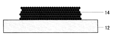
- FIG. 1 is a diagram schematically showing a cross-sectional structure of the dye-sensitized solar cell according to the present embodiment.
- FIG. 2A is a schematic diagram of a battery member structure for explaining a production process of the method for producing a dye-sensitized solar cell according to the present embodiment, and is a view for explaining a porous semiconductor layer forming process. It is.
- FIG. 2B is a schematic diagram of a battery member structure for explaining a production process of the method for producing a dye-sensitized solar cell according to the present embodiment, and is a view for explaining a mixed layer forming process. .
- FIG. 1 is a diagram schematically showing a cross-sectional structure of the dye-sensitized solar cell according to the present embodiment.
- FIG. 2A is a schematic diagram of a battery member structure for explaining a production process of the method for producing a dye-sensitized solar cell according to the present embodiment, and is a view for explaining a porous semiconductor
- FIG. 2C is a schematic diagram of the battery member structure for explaining the production process of the method for producing the dye-sensitized solar cell according to the present embodiment, and is a diagram for explaining the conductive metal film forming process. It is.
- FIG. 2 (D) is a schematic diagram of the battery member structure for explaining the production process of the method for producing the dye-sensitized solar cell according to the present embodiment, for explaining the fine particle layer disappearance process including the firing step.
- FIG. FIG. 2 (E) is a schematic diagram of the battery member structure for explaining the production process of the method for producing the dye-sensitized solar cell according to the present embodiment, and describes the fine particle layer disappearance process not including the firing step.
- FIG. FIG. 3 is a SEM photograph of the Ti film obtained in Example 1.
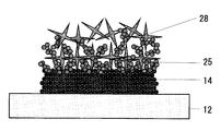
- a dye-sensitized solar cell 10 includes a transparent substrate 12, a porous semiconductor layer 14 that adsorbs a dye disposed on the transparent substrate 12, and a porous structure.
- a conductive metal film 16 disposed on the surface of the porous semiconductor layer 14 opposite to the transparent substrate 12, and a substrate 20 (conductive substrate) provided with the conductive film 18 provided to face the transparent substrate 12.
- An electrolyte 22 is provided between the conductive metal film 16 and the substrate 20 provided with the conductive film 18.
- reference numeral 23 indicates a spacer provided for sealing the electrolyte 22 in the battery.
- the deep hole-shaped through-hole 24 is a hole deep enough to ensure that a hole having a relatively small diameter penetrates the conductive metal film 16 even when the conductive metal film 16 is thick. This means, for example, a long cylindrical hole having a depth dimension several times or several tens of times larger than the diameter of the hole. Further, it has a large number of porous semiconductor particles 25 that penetrate through the conductive metal film 16 and have one end exposed to the electrolyte 22 and the other end joined to the porous semiconductor layer 14.
- the porous semiconductor particles 25 may be the same type as the material of the porous semiconductor layer 14 as the material, or different types of materials may be used. Also, the particle diameter of the porous semiconductor particles 25 may be the same as that of the material of the porous semiconductor layer 14, or materials having different particle diameters may be used.
- the shape of the porous semiconductor particles 25 is not particularly limited. For example, those having needle-like or elliptical columnar shape anisotropy can be used. In order to ensure that the porous semiconductor particles 25 penetrate the conductive metal film 16, it is preferable to adjust at least the dimension in the longitudinal direction to 100 nm or more. As the porous semiconductor particles 25, aggregates of particles having a primary particle diameter of 10 to 40 nm can be used.
- the porous semiconductor particles 25 are preferably fired at a temperature of 300 to 550 ° C., for example.
- the conductive metal film 16 is electrically connected to an external electrode (collector electrode) 26 provided on the periphery of the transparent substrate 12.
- the conductive metal film 16 may be provided inside the porous semiconductor layer 14.
- a plurality of conductive metal films 16 may be alternately formed with the porous semiconductor layer.
- the transparent substrate 12 and the substrate 20 may be glass plates or plastic plates, for example.
- a plastic plate for example, PET, PEN, polyimide, a cured acrylic resin, a cured epoxy resin, a cured silicone resin, various engineering plastics, a cyclic polymer obtained by metathesis polymerization, and the like can be given.
- the transparent substrate 12 may have a conductive film similar to the conductive film 18 described below provided on a substrate such as a glass plate.
- the conductive film 18 may be, for example, ITO (indium film doped with tin), FTO (tin oxide film doped with fluorine), or SnO 2 film.
- a catalyst film such as a platinum film is provided on the surface of the conductive film 18 facing the electrolyte (electrolytic solution) 22.
- the dye adsorbed on the porous semiconductor layer 14 has absorption at a wavelength of 400 nm to 1000 nm, and examples thereof include metal complexes such as ruthenium dye and phthalocyanine dye, and organic dyes such as cyanine dye.
- the electrolyte (electrolytic solution) 22 contains iodine, lithium ions, ionic liquid, t-butylpyridine, and the like.
- iodine a redox material composed of a combination of iodide ions and iodine can be used.
- the redox form contains an appropriate solvent that can dissolve the redox form.
- the thickness of the porous semiconductor layer 14 is not particularly limited, but is preferably 14 ⁇ m or more.
- a method for improving the conversion efficiency of sunlight a method of increasing the absorption efficiency of sunlight by increasing the thickness of the porous semiconductor layer is conceivable.
- the electron diffusion length exceeds the thickness dimension of the porous semiconductor layer, there is no effect even if the thickness of the porous semiconductor layer is further increased, and conversely the open circuit voltage is lowered and the conversion efficiency is lowered. There is.
- the dye-sensitized solar cell 10 according to the present embodiment electrons easily move in the porous semiconductor layer 14 via the conductive metal film 16 acting as a current collecting layer.
- the charge transfer resistance from the conductive metal film 16 to the electrolyte 22 is large and reverse electron transfer hardly occurs, high conversion efficiency can be obtained even when the thickness of the porous semiconductor layer 14 is increased to, for example, 14 ⁇ m or more. .
- the porous metal layer 25 has a large number of porous semiconductor particles 25 penetrating the conductive metal film 16 and having one end exposed to the electrolyte 22 and the other end bonded to the porous semiconductor layer 14, electrons are moved more smoothly. Contributes to the improvement of power generation efficiency.
- the upper limit of the thickness of the porous semiconductor layer 14 is appropriately set according to the value of the conversion efficiency to be obtained, and is, for example, about 40 ⁇ m. Needless to say, the present invention can be suitably applied to the case where the porous semiconductor layer 14 has a normal thickness.
- the porous semiconductor layer 14 is formed by baking a semiconductor material at a temperature of 300 ° C. or higher, more preferably 450 ° C. or higher.
- the temperature is sufficiently lower than the melting point of the material of the porous semiconductor layer 14, and more preferably 550 ° C. or less.
- titanium oxide titanium oxide
- it is preferably fired in a state of anatase crystal having high conductivity of titanium oxide at a temperature that does not shift to a rutile crystal.
- an oxide of a metal such as titanium, tin, zirconium, zinc, indium, tungsten, iron, nickel, or silver can be used.
- titanium oxide (titania) ) Is more preferable.
- the fine particles of titanium oxide include small particles having a particle size of 10 nm or less and large particles having a particle size of about 20 to 30 nm. When the former is made of a fine particle having a small particle size, a relatively dense film is formed. On the other hand, when the latter is made of a fine particle having a large particle size, a highly porous film is formed.
- the surface of the transparent conductive film such as tin oxide has irregularities, and it is desirable to use a relatively dense porous semiconductor layer 14 in order to cover the irregularities with good coverage.
- the porous semiconductor layer 14 has, for example, a two-layer structure, the first layer on the transparent conductive film side is formed of fine particles of titanium oxide having a small particle diameter, and the second layer formed on the surface of the first layer. Forming the layer with fine particles of titanium oxide having a larger particle size than the first layer is a preferred embodiment.
- the conductive metal film 16 preferably does not have at least the thermal history of the temperature necessary for firing the material of the porous semiconductor layer 14 and is sufficiently lower than 500 ° C., more preferably, Those having a heat history of about 200 ° C. or less, or those not substantially undergoing a heating step.
- the porous semiconductor layer 14 preferably has a hole communicating with the hole penetrating the conductive metal film 16.
- an appropriate metal can be selected and used as long as it has moderate conductivity.
- the metal includes not only a single metal but also a metal compound such as a metal oxide or an alloy.
- the conductive metal film 16 may have a metal surface covered with a dense oxide semiconductor such as titania.
- a corrosion-resistant metal from the viewpoint of reliably preventing the conductive metal film 16 from being corroded by the electrolyte 22 containing a redox material such as iodine.
- a corrosion-resistant metal tungsten (W), titanium (Ti), nickel (Ni), or a mixture thereof, or a metal compound thereof can be preferably used, but besides these, for example, the surface is passivated. Metal can be used.
- the conductive metal film 16 can be formed on the surface of the porous semiconductor layer 14 by a simple method such as a coating method, but is preferably formed by sputtering. At this time, for example, the end portion of the porous semiconductor layer 14 is shaved in advance by an appropriate method to form a connection portion with the external electrode 26.
- the thickness of the conductive metal film 16 is desirably as thick as possible from the viewpoint of reducing the sheet resistance of the film, and is preferably 100 nm or more, and more preferably 200 nm or more.
- the upper limit of the thickness of the conductive metal film 16 is not particularly limited, but is about 5 ⁇ m, for example.
- a plurality of conductive metal films 16 may be formed with a porous semiconductor layer interposed therebetween, that is, alternately with the porous semiconductor layer.
- a method for forming a large number of deep holes 24 formed in the conductive metal film 16 and a method for arranging the protruding porous semiconductor particles will be described later.
- the through holes 24 are irregularly arranged and formed innumerably depending on manufacturing conditions. However, it is sufficient that the through holes 24 are formed in an appropriate number as long as the electrolyte 22 can be sufficiently penetrated and permeated.
- the length (depth) of the through hole 24 is determined according to the thickness of the conductive metal film 16, and is preferably 100 nm to 5 ⁇ m.
- the deep hole-like through hole 24 has a higher diffusibility of the electrolyte 22 to the porous semiconductor layer 14 than a random small hole as in Non-Patent Document 1, for example.
- the diameter of the through hole 24 is not particularly limited, but is preferably 0.1 ⁇ m to 5 ⁇ m, and more preferably 0.2 ⁇ m to 3 ⁇ m.
- the transparent conductive film that is usually provided on the transparent substrate is omitted, and instead, disposed inside the porous semiconductor layer or on the surface opposite to the transparent substrate.
- the conductive metal film has a large number of deep holes in which the conductive metal film is irregularly formed, one end is exposed to the electrolyte through the conductive metal film, and the other end is Since it has a large number of porous semiconductor particles bonded to the porous semiconductor layer, it can be easily manufactured, and the power extraction efficiency is high.
- the conductive metal film is increased in thickness to increase the size. It can be set as the dye-sensitized solar cell suitable for.
- a mixed layer of fine particles having shape anisotropy that can be removed by heating or solvent washing is formed on the porous semiconductor layer.
- a mixed layer forming step, a conductive metal film forming step of forming a conductive metal film on the mixed layer, a fine particle layer disappearing step of disappearing fine particles (fine particles having shape anisotropy) by heating or solvent washing, Have
- the material of the porous semiconductor layer 14 is applied to the transparent substrate 12 to form the porous semiconductor layer 14 (see FIG. 2A).
- the porous semiconductor layer 14 refers to a material that is fired after the material of the porous semiconductor layer 14 is applied.
- porous semiconductor particles (particles used as a material for the porous semiconductor layer) 25 and fine particles 28 having shape anisotropy that can be removed by heating or solvent washing are mixed to prepare, for example, a paste-like mixture.
- a mixed layer is formed on the porous semiconductor layer 14 (see a mixed layer forming step in FIG. 2B).
- the mixed layer can be formed, for example, by dispersing a slurry of the mixture on the porous semiconductor layer 14 by electrospray. At this time, the mixed layer may be baked at a temperature of about 300 to 550 ° C., for example. Next, a conductive metal film 16 is formed on the mixed layer (refer to FIG. 2C).
- FIG. 2C schematically shows that the thickness of the mixed layer is about 10 times the thickness of the conductive metal film 16 for understanding the invention.
- the conductive metal film 16 is sufficient if it is about one to several times.
- the fine particles 28 are eliminated by heating or solvent cleaning (refer to FIG. 2D and FIG. 2E). As a result, a large number of deep holes 24, which are deep holes, are irregularly formed in the conductive metal film 16.
- porous semiconductor particle 25 that does not disappear by heating or solvent cleaning is joined to the porous semiconductor layer 14 and the other end is exposed from the conductive metal film 16.
- a porous semiconductor particle layer bonded to the porous semiconductor particles 25 is partially formed on the conductive metal film 16.
- the partially formed porous semiconductor particle layer may be left as it is or may be removed by an appropriate method.
- 2D shows a conductive metal film forming process when including the step of firing the mixed layer
- FIG. 2E shows the conductive metal film when not including the step of firing the mixed layer. A formation process is shown.
- the substrate 20 provided with the conductive film 18 is disposed opposite to the transparent substrate 12, sealed with the spacer 23, and injected with the electrolyte 22, thereby completing the dye-sensitized solar cell 10 (reference numerals 10, 18). , 20, 22 and 23, see FIG.
- the conductive metal film is electrically connected to an external electrode having an appropriate structure in an appropriate process.
- the material of the fine particles 28 to be used when removing the fine particle layer by heating, a material that is thermally decomposed and disappears at a temperature that does not cause thermal damage to the previously formed layer such as the porous semiconductor layer 14 is used. Bake at a temperature near the temperature.
- the temperature that does not cause thermal damage to a previously formed layer such as the porous semiconductor layer 14 is a temperature sufficiently lower than, for example, 500 ° C., and more preferably about 200 ° C. or less. Thereby, for example, the thermal influence on the conductive metal film 16 that may occur when the conductive metal film 16 is heated at a temperature of 500 ° C. or higher is also reduced.
- a combination of a solvent that does not cause chemical damage to a pre-formed layer such as a porous semiconductor layer and a fine particle material that can be easily removed by cleaning using the solvent is not particularly limited, but for example, a resin such as polystyrene or polymethyl methacrylate, or a metal oxide such as zinc oxide can be suitably used.
- the solvent used for solvent cleaning is not particularly limited, and may be appropriately selected according to the fine particle material.
- an organic solvent such as toluene capable of dissolving the resin, or dilute hydrochloric acid capable of dissolving the metal.
- An acid such as can be used.
- fine particles 28 formed of the above material those having shape anisotropy are used.
- fine particles preferably, fine particles having a large number of legs having apexes of polyhedrons or needle-shaped fine particles are used.
- the present invention is not limited thereto, and for example, oval spherical (for example, bean or rugby ball shape) fine particles may be used.
- a fine particle having a large number of legs with the apex of the polyhedron as the tip is used as the fine particle 28, for example, even when only one layer of the fine particle is dispersed on the porous semiconductor layer, the fine particle 28 is formed on the fine particle.
- the size of such fine particles varies depending on the thickness of the conductive metal film. For example, 1 to 30 ⁇ m.
- the acicular fine particles or the like can rise or stand on the porous semiconductor layer by, for example, being dispersed by an electronics spray method.
- the size of such needle-shaped fine particles is not particularly limited, but the length is appropriately set according to the thickness of the conductive metal film 16, and the needle-shaped fine particles are formed on the porous semiconductor layer 14. It is preferable to spray so as to overlap.
- the dimensions of the needle-shaped fine particles and the like can be the same as those of the fine particles having a number of legs with the apex of the polyhedron as the tip.
- a relatively stable conductive metal film 16 can be easily formed on the mixed layer by an appropriate method such as a vapor deposition method or a coating method, In the process in which fine particles disappear and are removed by solvent cleaning or the like, a large number of deep or large long cylindrical through-holes that are irregularly arranged in the conductive metal film 16 can be easily formed. it can. In addition, after the fine particles have disappeared and removed, the porous semiconductor particles 25 in which one end is joined to the porous semiconductor layer 14 and the other end is exposed from the conductive metal film 16 can be obtained.
- a mixed layer of conductive metal particles, porous semiconductor particles, and fine particles having shape anisotropy that can be removed by heating or solvent washing You may comprise so that it may have the mixed layer formation process formed on a porous semiconductor layer, and the fine particle layer disappearance process which lose
- the conductive metal film formed at this time is more firmly supported by the porous semiconductor particles.
- the mixed layer of the conductive metal particles that become the conductive metal film, the porous semiconductor particles, and the fine particles having shape anisotropy is formed in one step, the manufacturing process is simplified.
- the method for producing a dye-sensitized solar cell according to the present embodiment further includes a porous semiconductor layer stacking step of forming a porous semiconductor layer different from the porous semiconductor layer on the surface of the conductive metal film. You may comprise.
- the manufacturing method of the dye-sensitized solar cell according to the present embodiment described above the manufacturing method is simple, and the dye-sensitized solar cell according to the present embodiment can be suitably obtained.
- Titania paste (1 layer of HT paste, 5 layers of D paste: manufactured by Solaronics) was applied to a glass substrate to a thickness of 20 ⁇ m and baked at 500 ° C. for 30 minutes to form titania (titania layer, porous semiconductor layer).
- Zinc oxide tetrapod crystal (trade name: Panatetra, average fiber length of fiber part: about 10 ⁇ m, average fiber diameter: about 1 ⁇ m: manufactured by Amtec Co., Ltd.) and titanium oxide fine particles (trade name: AEROXIDE (registered trademark))
- a mixed composition slurry of TiO2P25, an average primary particle size of about 20 nm, and an aggregate size of 200 nm was dispersed by an electrospray method. The composition in the mixture was adjusted to a ratio of 50:50 zinc oxide fiber and titania fine particles. After electrospray dispersion, baking was performed at 500 ° C. for 30 minutes.
- Ti layer a Ti film (Ti layer) was formed by sputtering (film thickness 300 nm). The remaining tetrapod type crystals were removed by rinsing with dilute hydrochloric acid to produce a conductive Ti layer.
- An SEM photograph of the Ti film obtained at this time is shown in FIG. A deep hole-like through-hole group (black portion in FIG. 3) formed in the Ti film (underlying portion in FIG. 3) and a porous semiconductor particle group (FIG. 3) with the tip exposed through the Ti film. Among them, white particles or gray particle portions similar to the base) can be observed.
- the counter electrode fluorine-doped tin oxide glass (manufactured by Solaronics) subjected to platinum sputtering was used.
- the substrate on which the Ti layer was formed and the counter electrode were sealed with a 50 ⁇ m thick spacer (High Milan, Mitsui DuPont).
- An electrolyte solution composed of an acetonitrile solution of iodine 40 mM, LiI 500 mM, and t-Butylpyridine 580 mM was injected into the obtained cell to produce a 5 mm square battery (battery cell).
- the characteristics of the produced solar cells were evaluated by irradiating the dye-sensitized solar cells with AM1.5 and 100 mW / cm2 pseudo-sunlight using a solar simulator. As a result, an efficiency of 10.8% was obtained.
- Example 2 A titania paste (1 layer of HT paste, 5 layers of D paste: manufactured by Solaronics) was applied to a glass substrate to a thickness of 20 ⁇ m and baked at 500 ° C. for 30 minutes to form titania (titania layer, porous semiconductor layer).
- Zinc oxide tetrapod crystal (trade name: Panatetra, average fiber length of fiber part: about 10 ⁇ m, average fiber diameter: about 1 ⁇ m: manufactured by Amtec Co., Ltd.) and titanium oxide fine particles (trade name: AEROXIDE (registered trademark))
- a mixed composition slurry of TiO2P25, an average primary particle size of about 20 nm, and an aggregate size of 200 nm was dispersed by an electrospray method.
- the composition in the mixture was prepared in a 50:50 ratio of zinc oxide fibers and titania microparticles. Thereafter, a Ti film (Ti layer) was formed by sputtering (film thickness 300 nm).
- the counter electrode fluorine-doped tin oxide glass (manufactured by Solaronics) subjected to platinum sputtering was used.
- the substrate on which the Ti layer was formed and the counter electrode were sealed with a 50 ⁇ m-thick spacer (High Milan, Mitsui DuPont).
- An electrolyte solution composed of an acetonitrile solution of iodine 40 mM, LiI 500 mM, and t-Butylpyridine 580 mM was injected into the obtained cell to produce a 5 mm square battery (battery cell).
- the characteristics of the produced solar cell were measured and evaluated by irradiating the dye-sensitized solar cell with AM1.5 and 100 mW / cm2 pseudo-sunlight using a solar simulator, and an efficiency of 10.6% was obtained.
- Tia paste (1 layer of HT paste, 5 layers of D paste: manufactured by Solaronics) was applied to a glass substrate to a thickness of 20 ⁇ m and baked at 500 ° C. for 30 minutes to form titania (titania layer, porous semiconductor layer).
- Zinc oxide tetrapod type crystals (trade name: Panatetra, average fiber length of fiber part: about 10 ⁇ m: manufactured by Amtec Co., Ltd.) were dispersed on the titania surface of the fired substrate by an electrospray method. Thereafter, a Ti film (Ti layer) was formed by sputtering (film thickness 300 nm).
- the substrate on which the Ti layer was formed and the counter electrode were sealed with a 50 ⁇ m thick spacer (High Milan: Mitsui DuPont).
- An electrolyte solution composed of an acetonitrile solution of iodine 40 mM, LiI 500 mM, and t-Butylpyridine 580 mM was injected into the obtained cell to produce a 5 mm square battery (battery cell).
- an efficiency of 9.5% was obtained.
- Tia paste (1 layer of HT paste, 5 layers of D paste: manufactured by Solaronics) was applied to a glass substrate to a thickness of 20 ⁇ m and baked at 500 ° C. for 30 minutes to form titania (titania layer, porous semiconductor layer). Fine particles of titanium oxide (trade name: AEROXIDE Ⓡ TiO2 P25, average primary particle diameter of about 20 nm, aggregate size: 200 nm: manufactured by Nippon Aerosil Co., Ltd.) were dispersed on the titania surface of the fired substrate by electrospray method. Thereafter, a Ti film (Ti layer) was formed by sputtering (film thickness 300 nm).
- An electrolyte solution composed of an acetonitrile solution of iodine 40 mM, LiI 500 mM, and t-Butylpyridine 580 mM was injected into the obtained cell to produce a 5 mm square battery (battery cell).
- an efficiency of 6.0% was obtained.
Landscapes
- Engineering & Computer Science (AREA)
- Power Engineering (AREA)
- Microelectronics & Electronic Packaging (AREA)
- Physics & Mathematics (AREA)
- Condensed Matter Physics & Semiconductors (AREA)
- Electromagnetism (AREA)
- General Physics & Mathematics (AREA)
- Computer Hardware Design (AREA)
- Manufacturing & Machinery (AREA)
- Hybrid Cells (AREA)
- Photovoltaic Devices (AREA)
- Cell Electrode Carriers And Collectors (AREA)
Abstract
Description
色素増感太陽電池は、材料が安価であり、作製に大掛かりな設備を必要としないことから、低コストの太陽電池として注目されている。 The dye-sensitized solar cell is called a wet solar cell or a Gretzel battery, and is characterized in that it has an electrochemical cell structure typified by an iodine solution without using a silicon semiconductor. Specifically, a porous semiconductor layer such as a titania layer formed by baking titanium dioxide powder or the like on a transparent conductive glass plate (transparent conductive substrate on which a transparent conductive film is laminated) and adsorbing a pigment to the titanium dioxide powder. It has a simple structure in which an iodine solution or the like is disposed as an electrolytic solution between counter electrodes made of a conductive glass plate (conductive substrate).
Dye-sensitized solar cells are attracting attention as low-cost solar cells because they are inexpensive and do not require large-scale equipment for production.
そのうちのひとつとして、電極の導電性の改善による電力取り出し効率の向上を図るために、光入射側に設けられる透明導電性基板上に通常形成される透明導電膜を省略することが検討されている。これは、太陽電池を大型化する際に特に大きな意義を持つ。 Dye-sensitized solar cells are required to further improve the conversion efficiency of sunlight, and have been studied from various viewpoints.
As one of them, in order to improve the power extraction efficiency by improving the conductivity of the electrode, it is considered to omit the transparent conductive film normally formed on the transparent conductive substrate provided on the light incident side. . This is particularly significant when the size of the solar cell is increased.
また、例えば、ガラス基板上に、半導体微粒子層、金属網、電荷移動層および対極をこの順番で含む積層部を有し、金属網と電荷移動層が直接接した構造の光電変換素子が開示されている(特許文献1参照)。 For example, a Ti thin film with a hole formed by directly providing a TiO 2 porous semiconductor layer adsorbing a dye on a transparent substrate without a transparent conductive film and sputtering Ti on the surface of the porous semiconductor layer is used as a collector electrode. A dye-sensitized solar cell is disclosed (see Non-Patent Document 1). The solar conversion efficiency of this battery is reported to be 3.6%.
Further, for example, a photoelectric conversion element having a structure in which a semiconductor fine particle layer, a metal network, a charge transfer layer, and a counter electrode are stacked in this order on a glass substrate and the metal network and the charge transfer layer are in direct contact with each other is disclosed. (See Patent Document 1).
また、特許文献1のものは、製造方法として煩雑であり、製造コストが高くなるおそれがある。 However, in Non-Patent Document 1, although there is no mention of the thickness or aperture ratio of the Ti thin film, the porous semiconductor layer is formed when the thickness of the Ti thin film formed by sputtering is extremely thin, for example, about 20 nm. Although holes can be formed in the Ti thin film formed on the unevenness of the TiO 2 particles on the surface, there is a possibility that the area resistance (sheet resistance) of the Ti thin film becomes large and does not lead to a significant improvement in power extraction efficiency. On the other hand, if the thickness of the Ti thin film is increased to, for example, about several hundreds of nanometers in order to reduce the area resistance of the Ti thin film, no hole is formed in the Ti thin film, and the electrolyte penetrates into the porous semiconductor layer May be blocked and may not function as a solar cell.
Moreover, the thing of patent document 1 is complicated as a manufacturing method, and there exists a possibility that manufacturing cost may become high.
これによれば、色素増感太陽電池を簡易に製造することができ、多孔質半導体層の厚みを厚くする等した場合においても高い変換効率を得ることができる。 In view of these problems, the present inventors have a conductive property having a large number of irregularly arranged through holes on the inside of the porous semiconductor layer or on the surface opposite to the light-introducing side of the transparent substrate. A dye-sensitized solar cell having a metal film is disclosed (Patent Document 2).
According to this, a dye-sensitized solar cell can be easily manufactured, and high conversion efficiency can be obtained even when the thickness of the porous semiconductor layer is increased.
該導電性金属膜が不規則に形成される深い孔状の多数の貫通孔を有するとともに、該導電性金属膜を貫通して一端が電解質に露出し、他端が該多孔質半導体層に接合する多数の多孔質半導体粒子を有し、該導電性金属膜が外部電極に接続されることを特徴とする。 The dye-sensitized solar cell according to the present invention includes a transparent substrate, a porous semiconductor layer adsorbing a dye disposed on the transparent substrate, and the inside of the porous semiconductor layer or the opposite side of the transparent substrate. A dye-sensitized solar cell comprising a conductive metal film disposed on a surface and a conductive substrate provided to face the transparent substrate, and having an electrolyte between the conductive metal film and the conductive substrate. ,
The conductive metal film has a large number of deep hole-like through holes formed irregularly, one end is exposed to the electrolyte through the conductive metal film, and the other end is joined to the porous semiconductor layer. A plurality of porous semiconductor particles, and the conductive metal film is connected to an external electrode.
多孔質半導体粒子と加熱によりまたは溶剤洗浄により除去可能な、形状異方性を有する微粒子の混合層を多孔質半導体層上に形成する混合層形成工程と、
該混合層の表面に導電性金属膜を形成する導電性金属膜形成工程と、
加熱によりまたは溶剤洗浄により該微粒子を消失させる微粒子消失工程と、
を有することを特徴とする。 Moreover, the method for producing a dye-sensitized solar cell according to the present invention is a method for producing the above dye-sensitized solar cell,
A mixed layer forming step of forming a mixed layer of fine particles having shape anisotropy on the porous semiconductor layer, which can be removed by heating or solvent washing with the porous semiconductor particles;
A conductive metal film forming step of forming a conductive metal film on the surface of the mixed layer;
A fine particle disappearance step of disappearing the fine particles by heating or solvent washing;
It is characterized by having.
導電性金属粒子と、多孔質半導体粒子と、加熱によりまたは溶剤洗浄により除去可能な、形状異方性を有する微粒子との混合層を多孔質半導体層上に形成する混合層形成工程と、
溶剤洗浄により該微粒子を消失させる微粒子層消失工程と、
を有することを特徴とする。 Moreover, the method for producing a dye-sensitized solar cell according to the present invention is a method for producing the above dye-sensitized solar cell,
Forming a mixed layer of conductive metal particles, porous semiconductor particles, and fine particles having shape anisotropy, which can be removed by heating or solvent washing, on the porous semiconductor layer; and
A fine particle layer disappearance step of eliminating the fine particles by solvent washing;
It is characterized by having.
また、本発明に係る色素増感太陽電池の製造方法は、上記の色素増感太陽電池の製造方法であって、加熱によりまたは溶剤洗浄により除去可能な、形状異方性を有する微粒子を導電性金属膜の孔の形成に用いるとともに、多孔質半導体粒子を微粒子と混合して用いるため、上記の色素増感太陽電池を好適に得ることができる。 The dye-sensitized solar cell according to the present invention includes a conductive metal film disposed on the inside of the porous semiconductor layer or on the surface opposite to the transparent substrate, and deep holes in which the conductive metal film is irregularly formed. A large number of through-holes, and one end exposed to the electrolyte through the conductive metal film and the other end joined to the porous semiconductor layer. Therefore, it is possible to obtain a dye-sensitized solar cell suitable for enlargement by increasing the thickness of the conductive metal film.
The method for producing a dye-sensitized solar cell according to the present invention is a method for producing the above-described dye-sensitized solar cell, wherein fine particles having shape anisotropy that can be removed by heating or solvent washing are electrically conductive. Since it is used for forming pores of the metal film and the porous semiconductor particles are mixed with the fine particles, the above dye-sensitized solar cell can be suitably obtained.
多孔質半導体粒子25は、形状を特に限定するものではない。例えば、針状や楕円柱状の形状異方性を有するものを用いることができる。
多孔質半導体粒子25は、導電性金属膜16を確実に貫通させるためには、少なくとも長手方向の寸法を100nm以上に調製することが好ましい。
多孔質半導体粒子25は、10~40nmの一次粒子径を有する粒子の凝集物を用いることができる。
多孔質半導体粒子25は、例えば300~550℃の温度で焼成することが好ましい。 The
The shape of the
In order to ensure that the
As the
The
透明基板12は、以下に説明する導電膜18と同様の導電膜をガラス板等の基板上に設けたものであってもよい。
導電膜18は、例えば、ITO(スズをドープしたインジウム膜)であってもよく、またFTO(フッ素をドープした酸化スズ膜)であってもよく、あるいはまたSnO2膜であってもよい。導電膜18の電解質(電解液)22に向けた面には、例えば白金膜等の触媒膜を設ける。 The
The
The
太陽光の変換効率を向上させる方法のひとつとして、多孔質半導体層の厚みを厚くして太陽光の吸収効率を上げる方法が考えられる。しかしながら、電子拡散長が多孔質半導体層の厚み寸法を超えてしまうと、それ以上多孔質半導体層の厚みを厚くしても効果がなく、逆に開放電圧が低下し、変換効率が低下する問題がある。
これに対して、本実施の形態に係る色素増感太陽電池10によれば、集電層として作用する導電性金属膜16を介して多孔質半導体層14内を電子が容易に移動し、また、導電性金属膜16から電解質22への電荷移動抵抗が大きく、逆電子移動が起こりにくいため、多孔質半導体層14の厚みを例えば14μm以上に厚くした場合においても高い変換効率を得ることができる。また、導電性金属膜16を貫通して一端が電解質22に露出し、他端が多孔質半導体層14に接合する多数の多孔質半導体粒子25を有するため、電子の移動がより円滑に行われ、発電効率の向上に寄与する。
多孔質半導体層14の厚みの上限は得られる変換効率の値等に応じて適宜設定されるが、例えば、40μm程度である。なお、本発明を多孔質半導体層14が通常の厚みを有する場合にも本発明を好適に適用できることは勿論である。 The thickness of the
As a method for improving the conversion efficiency of sunlight, a method of increasing the absorption efficiency of sunlight by increasing the thickness of the porous semiconductor layer is conceivable. However, if the electron diffusion length exceeds the thickness dimension of the porous semiconductor layer, there is no effect even if the thickness of the porous semiconductor layer is further increased, and conversely the open circuit voltage is lowered and the conversion efficiency is lowered. There is.
On the other hand, according to the dye-sensitized
The upper limit of the thickness of the
多孔質半導体層14の半導体材料として、例えば、チタン、スズ、ジルコニウム、亜鉛、インジウム、タングステン、鉄、ニッケルあるいは銀等の金属の酸化物を用いることができるが、このうち、チタン酸化物(チタニア)がより好ましい。
チタン酸化物の微粒子には、粒径が10nm以下の小さなものや20~30nm程度の大きなものなどがある。前者の粒径が小さい微粒子で膜を作った場合、比較的緻密な膜ができ、一方、後者の粒径が大きい微粒子で膜を作った場合には、多孔性の高い膜が形成される。酸化錫のような透明導電膜の表面には凹凸があり、その凹凸をカバレッジ良く覆うために、比較的緻密な多孔質半導体層14を用いることが望ましい。このため、多孔質半導体層14を例えば二層構成とし、透明導電膜側の第1層を粒径が小さいチタン酸化物の微粒子で形成し、第1層の表面に形成される第2
層を粒径が第1層に比べて大きなチタン酸化物の微粒子で形成することは好ましい実施態様である。 The
As a semiconductor material of the
The fine particles of titanium oxide include small particles having a particle size of 10 nm or less and large particles having a particle size of about 20 to 30 nm. When the former is made of a fine particle having a small particle size, a relatively dense film is formed. On the other hand, when the latter is made of a fine particle having a large particle size, a highly porous film is formed. The surface of the transparent conductive film such as tin oxide has irregularities, and it is desirable to use a relatively dense
Forming the layer with fine particles of titanium oxide having a larger particle size than the first layer is a preferred embodiment.
導電性金属膜16は、適度の導電性を有するものである限り、適宜の金属を選定して用いることができる。ここで、金属とは、金属単体のみでなく、金属酸化物等の金属化合物や合金を含む。
導電性金属膜16は、金属の表面を緻密な酸化物半導体、例えばチタニアにより被覆したものであってもよい。ただし、ヨウ素等の酸化還元体を含む電解質22による導電性金属膜16の腐食を確実に防ぐ観点からは、耐食性金属を用いることがより好ましい。耐食性金属としては、タングステン(W)、チタン(Ti)もしくはニッケル(Ni)またはこれらの混合物、あるいはこれらの金属化合物を好適に用いることができるが、これら以外にも、例えば表面を不動態化した金属を用いることができる。 The
As the
The
導電性金属膜16の厚みは、膜の面積抵抗を小さくする観点からは厚ければ厚い方が望ましく、好ましくは100nm以上であり、より好ましくは200nm以上である。導電性金属膜16の厚みの上限は特に限定するものではないが、例えば5μm程度である。
また、導電性金属膜16は、多孔質半導体層を間に挟んで、すなわち、多孔質半導体層と交互に複数形成してもよい。
導電性金属膜16に形成される深い孔状の多数の貫通孔24の形成方法ならびに突起状の多孔質半導体粒子の配置方法については後述する。貫通孔24は、不規則に配置され、製造条件によっては無数に形成されるが、電解質22を十分に浸透、透過できるものである限り適当な数形成されれば十分である。貫通孔24の長さ(深さ)は、導電性金属膜16の厚みに対応して定まるものであるが、好ましくは、100nm~5μmである。深い孔状の貫通孔24は、例えば、非特許文献1のようなランダムな小さい孔に比べて電解質22の多孔質半導体層14への拡散性が高い。貫通孔24の径は、特に限定するものではないが、0.1μm~5μmであることが好ましく、0.2μm~3μmであることがより好ましい。 The
The thickness of the
Further, a plurality of
A method for forming a large number of
本実施の形態に係る色素増感太陽電池の製造方法は、多孔質半導体粒子と加熱によりまたは溶剤洗浄により除去可能な、形状異方性を有する微粒子の混合層を多孔質半導体層上に形成する混合層形成工程と、混合層上に導電性金属膜を形成する導電性金属膜形成工程と、加熱によりまたは溶剤洗浄により微粒子(形状異方性を有する微粒子)を消失させる微粒子層消失工程と、を有する。 Here, the manufacturing method of the dye-sensitized solar cell which concerns on this Embodiment suitable as a manufacturing method of the dye-sensitized solar cell which concerns on this Embodiment is demonstrated.
In the method for producing a dye-sensitized solar cell according to the present embodiment, a mixed layer of fine particles having shape anisotropy that can be removed by heating or solvent washing is formed on the porous semiconductor layer. A mixed layer forming step, a conductive metal film forming step of forming a conductive metal film on the mixed layer, a fine particle layer disappearing step of disappearing fine particles (fine particles having shape anisotropy) by heating or solvent washing, Have
まず、透明基板12に多孔質半導体層14の材料を塗布し多孔質半導体層14を形成する(図2(A)参照)。ここで、多孔質半導体層14は、多孔質半導体層14の材料を塗布した後、焼成したものをいう。
ついで、多孔質半導体粒子(多孔質半導体層の材料として用いられる粒子)25と加熱によりまたは溶剤洗浄により除去可能な、形状異方性を有する微粒子28を混合して例えばペースト状の混合物を調製して多孔質半導体層14上に配置して混合層を形成する(混合層形成工程 図2(B)参照)。このとき、微粒子28として例えば微細なファイバー形状の材料を単独で使用するとだま(粒状の塊)になるおそれがあるが、多孔質半導体粒子25を併用することにより、からまりを抑制する効果がある。混合層は、例えば混合物のスラリーをエレクトロスプレーで多孔質半導体層14上に分散させることによって形成することができる。このとき、引き続き、例えば300~550℃程度の温度で混合層に焼成処理を実施してもよい。
ついで、混合層上に導電性金属膜16を形成する(導電性金属膜形成工程 図2(C)参照)。このとき、形状異方性を有する微粒子28と多孔質半導体粒子25の混合物は、導電性金属膜16を貫通して、図2(C)中、混合物の上端が露出し、さらには混合物の一部が全体として露出する。なお、図2(C)は、発明の理解のために混合層の厚みが導電性金属膜16の厚みの10倍近くの厚みであるように模式的に示しているが、混合層の厚みは、導電性金属膜16の一倍~数倍程度であれば十分である。
ついで、加熱によりまたは溶剤洗浄により微粒子28を消失させる(微粒子消失工程 図2(D)、図2(E)参照)。これにより、導電性金属膜16に多数の深い孔である貫通孔24が不規則に形成される。また、このとき、加熱によりまたは溶剤洗浄によっては消失しない多孔質半導体粒子25は、一端が多孔質半導体層14と接合されるとともに他端が導電性金属膜16から露出する。なお、混合層の厚みが導電性金属膜16の厚みよりも大きいときは、導電性金属膜16上に多孔質半導体粒子25と接合された多孔質半導体粒子層が部分的に形成される。部分的に形成される多孔質半導体粒子層は、そのまま残してもよく、また、適当な方法で除去してもよい。
なお、図2(D)は、混合層を焼成するステップを含むときの導電性金属膜形成工程を示し、図2(E)は、混合層を焼成するステップを含まないときの導電性金属膜形成工程を示す。 Hereinafter, a manufacturing example will be specifically described with reference to FIGS. 2A to 2D schematically showing the manufacturing process.
First, the material of the
Next, porous semiconductor particles (particles used as a material for the porous semiconductor layer) 25 and
Next, a
Subsequently, the
2D shows a conductive metal film forming process when including the step of firing the mixed layer, and FIG. 2E shows the conductive metal film when not including the step of firing the mixed layer. A formation process is shown.
さらに、導電膜18を備えた基板20を透明基板12に対向配置し、スペーサ23で封止するとともに、電解質22を注入することで、色素増感太陽電池10が完成する(参照符号10、18、20、22および23については図1参照)。なお、先に本実施の形態に係る色素増感太陽電池の説明のところで触れたように、導電性金属膜は、適宜の工程において、適宜の構成とされる外部電極に電気的に接続させる。 Next, a dye is attached to the
Further, the
このような微粒子材料は、特に限定するものではないが、例えばポリスチレンやポリメタクリル酸メチル等の樹脂や酸化亜鉛等の金属酸化物を好適に用いることができる。また、溶剤洗浄に用いる溶剤は、特に限定するものではなく、微粒子材料に合わせて適宜選択すればよく、例えば樹脂を溶解することができるトルエン等の有機溶剤や、金属を溶解することができる希塩酸などの酸を用いることができる。 As the material of the
Such a particulate material is not particularly limited, but for example, a resin such as polystyrene or polymethyl methacrylate, or a metal oxide such as zinc oxide can be suitably used. Further, the solvent used for solvent cleaning is not particularly limited, and may be appropriately selected according to the fine particle material. For example, an organic solvent such as toluene capable of dissolving the resin, or dilute hydrochloric acid capable of dissolving the metal. An acid such as can be used.
微粒子28として多面体の頂点を先端とする多数の足を有する微粒子を用いる場合、例えば、微粒子が多孔質半導体層の上に1層のみ散布等されたときであっても、微粒子上に形成される適度に厚みの厚い導電性金属膜を確実に貫通して孔を形成することができる程度の寸法を有することが好ましく、そのような微粒子の寸法は、導電性金属膜の厚みに応じて異なるが、例えば1~30μmである。
一方、微粒子28として針状微粒子や楕円球微粒子を用いる場合、例えばエレクトロニクススプレイ法により散布することで、針状微粒子等を多孔質半導体層の上に起き上がり、あるいは立った状態とすることができる。このため、そのような針状微粒子等の寸法は特に限定するものではないが、導電性金属膜16の厚みに応じて適度の長さとし、また、多孔質半導体層14の上に針状微粒子等が重なり合うように散布することが好ましい。針状微粒子等の寸法は、上記多面体の頂点を先端とする多数の足を有する微粒子の同様の寸法とすることができる。
これらの形状異方性を有する微粒子28を多孔質半導体層14上に配置することで、微粒子を消失させた後の多孔質半導体層14にも深い孔が形成される。そして、上記導電性金属膜16を貫通する孔と連通するこの深い孔を介して孔質半導体層14の内部での電解質22の浸透、拡散がより良好に行われる。 As the
In the case where a fine particle having a large number of legs with the apex of the polyhedron as the tip is used as the
On the other hand, in the case where acicular fine particles or elliptical fine particles are used as the
By disposing these
また、微粒子が消滅、除去した後に、一端が多孔質半導体層14と接合されるとともに他端が導電性金属膜16から露出する多孔質半導体粒子25を得ることができる。 By the method for manufacturing a dye-sensitized solar cell according to the present embodiment, a relatively stable
In addition, after the fine particles have disappeared and removed, the
この方法によれば、このとき形成される導電性金属膜は、多孔質半導体粒子によってより強固に支持される。また、導電性金属膜となる導電性金属粒子と多孔質半導体粒子および形状異方性を有する微粒子の混合層を1つの工程で形成するため、製造工程が簡略化される。 In the method for producing a dye-sensitized solar cell according to the present embodiment, a mixed layer of conductive metal particles, porous semiconductor particles, and fine particles having shape anisotropy that can be removed by heating or solvent washing You may comprise so that it may have the mixed layer formation process formed on a porous semiconductor layer, and the fine particle layer disappearance process which lose | disappears microparticles | fine-particles by heating or solvent washing.
According to this method, the conductive metal film formed at this time is more firmly supported by the porous semiconductor particles. Moreover, since the mixed layer of the conductive metal particles that become the conductive metal film, the porous semiconductor particles, and the fine particles having shape anisotropy is formed in one step, the manufacturing process is simplified.
ガラス基板にチタニアペースト(HT ペースト1層、Dペースト5層:ソラロニクス社製)を20μmの厚みに塗布し、500℃で30分焼成してチタニア(チタニア層、多孔質半導体層)を形成した。焼成基板のチタニア表面に酸化亜鉛のテトラポッド型結晶(商品名パナテトラ、ファイバー部位の平均繊維長約10μm 平均繊維径約1μm:株式会社アムテック製)と酸化チタンの微粒子(商品名AEROXIDE(登録商標) TiO2P25、一次粒子の平均粒子径 約20nm、凝集体サイズ200nm:日本アエロジル(株)製)との混合組成物スラリーをエレクトロスプレー法により分散した。混合物中の組成は、酸化亜鉛ファイバーとチタニア微粒子を50:50の比率で調整した。エレクトロスプレー分散後、500℃で30分焼成した。この後、スパッタ法によりTi膜(Ti層)を形成した(膜厚300nm)。残存するテトラポッド型結晶を希塩酸でリンスすることにより、取り除き、導電性Ti層を作製した。
このとき得られるTi膜のSEM写真を図3に示す。Ti膜(図3中、下地部分)中に形成された深い孔状の貫通孔群(図3中、黒い部分)と、Ti膜を貫通して先端が露出する多孔質半導体粒子群(図3中、白い粒子あるいは下地と同様の灰色の粒子部分)を観察することができる。
ついで、0.05 wt %の色素溶液(ブラックダイ、アセトニトリル:tブチルアルコール=1:1:ソラロニクス社製)に上記のTi層を形成した基板を浸漬した(20時間)。
対極には白金スパッタ処理を行ったフッ素ドープ酸化錫ガラス(ソラロニクス社製)を使った。Ti層を形成した基板と対極を50μm厚のスペーサー(ハイミラン、三井デュポン社)で封止した。得られたセルの中に、ヨウ素40mM, LiI 500mM, t-Butylpyridine 580mM のアセトニトリル溶液からなる電解液を注入して、5mm角の電池(電池セル)を作製した。
作製した太陽電池特性を、ソーラーシミュレータを用いAM1.5、100mW/cm2の擬似太陽光を色素増感太陽電池に照射し、測定して評価したところ、10.8%の効率を得た。 Example 1
Titania paste (1 layer of HT paste, 5 layers of D paste: manufactured by Solaronics) was applied to a glass substrate to a thickness of 20 μm and baked at 500 ° C. for 30 minutes to form titania (titania layer, porous semiconductor layer). Zinc oxide tetrapod crystal (trade name: Panatetra, average fiber length of fiber part: about 10μm, average fiber diameter: about 1μm: manufactured by Amtec Co., Ltd.) and titanium oxide fine particles (trade name: AEROXIDE (registered trademark)) A mixed composition slurry of TiO2P25, an average primary particle size of about 20 nm, and an aggregate size of 200 nm (produced by Nippon Aerosil Co., Ltd.) was dispersed by an electrospray method. The composition in the mixture was adjusted to a ratio of 50:50 zinc oxide fiber and titania fine particles. After electrospray dispersion, baking was performed at 500 ° C. for 30 minutes. Thereafter, a Ti film (Ti layer) was formed by sputtering (film thickness 300 nm). The remaining tetrapod type crystals were removed by rinsing with dilute hydrochloric acid to produce a conductive Ti layer.
An SEM photograph of the Ti film obtained at this time is shown in FIG. A deep hole-like through-hole group (black portion in FIG. 3) formed in the Ti film (underlying portion in FIG. 3) and a porous semiconductor particle group (FIG. 3) with the tip exposed through the Ti film. Among them, white particles or gray particle portions similar to the base) can be observed.
Then, the substrate on which the Ti layer was formed was immersed in a 0.05 wt% dye solution (black dye, acetonitrile: tbutyl alcohol = 1: 1: manufactured by Solaronics) (20 hours).
As the counter electrode, fluorine-doped tin oxide glass (manufactured by Solaronics) subjected to platinum sputtering was used. The substrate on which the Ti layer was formed and the counter electrode were sealed with a 50 μm thick spacer (High Milan, Mitsui DuPont). An electrolyte solution composed of an acetonitrile solution of iodine 40 mM, LiI 500 mM, and t-Butylpyridine 580 mM was injected into the obtained cell to produce a 5 mm square battery (battery cell).
The characteristics of the produced solar cells were evaluated by irradiating the dye-sensitized solar cells with AM1.5 and 100 mW / cm2 pseudo-sunlight using a solar simulator. As a result, an efficiency of 10.8% was obtained.
ガラス基板にチタニアペースト(HT ペースト1層、Dペースト5層:ソラロニクス社製)を20μmの厚みに塗布し、500℃で30分焼成してチタニア(チタニア層、多孔質半導体層)を形成した。焼成基板のチタニア表面に酸化亜鉛のテトラポッド型結晶(商品名パナテトラ、ファイバー部位の平均繊維長約10μm 平均繊維径約1μm:株式会社アムテック製)と酸化チタンの微粒子(商品名AEROXIDE(登録商標) TiO2P25、一次粒子の平均粒子径 約20nm、凝集体サイズ200nm:日本アエロジル(株)製)との混合組成物スラリーをエレクトロスプレー法により分散した。前記混合物中の組成は、酸化亜鉛ファイバーとチタニア微粒子と50:50の比率で調製された。この後、スパッタ法によりTi膜(Ti層)を形成した(膜厚300nm)。残存するテトラポッド型結晶を希塩酸でリンスすることにより、取り除き、導電性Ti層を作製した。
このとき得られるTi膜のSEM写真を図3に示す。Ti膜(図3中、下地部分)中に形成された深い孔状の貫通孔群(図3中、黒い部分)と、Ti膜を貫通して先端が露出する多孔質半導体粒子群(図3中、白い粒子あるいは下地と同様の灰色の粒子部分)を観察することができる。
ついで、0.05 wt %の色素溶液(ブラックダイ、アセトニトリル:tブチルアルコール=1:1:ソラロニクス社製)に上記のTi層を形成した基板を浸漬した(20時間)。
対極には白金スパッタ処理を行ったフッ素ドープ酸化錫ガラス(ソラロニクス社製)を使った。Ti層を形成した基板と対極を50μm厚のスペーサー(ハイミラン、三井デュポン社)で封止した。得られたセルの中に、ヨウ素40mM, LiI 500mM, t-Butylpyridine 580mM のアセトニトリル溶液からなる電解液を注入して、5mm角の電池(電池セル)を作製した。
作製した太陽電池特性を、ソーラーシミュレータを用いAM1.5、100mW/cm2の擬似太陽光を色素増感太陽電池に照射し、測定して評価したところ、10.6%の効率を得た。 (Example 2)
A titania paste (1 layer of HT paste, 5 layers of D paste: manufactured by Solaronics) was applied to a glass substrate to a thickness of 20 μm and baked at 500 ° C. for 30 minutes to form titania (titania layer, porous semiconductor layer). Zinc oxide tetrapod crystal (trade name: Panatetra, average fiber length of fiber part: about 10μm, average fiber diameter: about 1μm: manufactured by Amtec Co., Ltd.) and titanium oxide fine particles (trade name: AEROXIDE (registered trademark)) A mixed composition slurry of TiO2P25, an average primary particle size of about 20 nm, and an aggregate size of 200 nm (produced by Nippon Aerosil Co., Ltd.) was dispersed by an electrospray method. The composition in the mixture was prepared in a 50:50 ratio of zinc oxide fibers and titania microparticles. Thereafter, a Ti film (Ti layer) was formed by sputtering (film thickness 300 nm). The remaining tetrapod type crystals were removed by rinsing with dilute hydrochloric acid to produce a conductive Ti layer.
An SEM photograph of the Ti film obtained at this time is shown in FIG. A deep hole-like through-hole group (black portion in FIG. 3) formed in the Ti film (underlying portion in FIG. 3) and a porous semiconductor particle group (FIG. 3) with the tip exposed through the Ti film. Among them, white particles or gray particle portions similar to the base) can be observed.
Then, the substrate on which the Ti layer was formed was immersed in a 0.05 wt% dye solution (black dye, acetonitrile: tbutyl alcohol = 1: 1: manufactured by Solaronics) (20 hours).
As the counter electrode, fluorine-doped tin oxide glass (manufactured by Solaronics) subjected to platinum sputtering was used. The substrate on which the Ti layer was formed and the counter electrode were sealed with a 50 μm-thick spacer (High Milan, Mitsui DuPont). An electrolyte solution composed of an acetonitrile solution of iodine 40 mM, LiI 500 mM, and t-Butylpyridine 580 mM was injected into the obtained cell to produce a 5 mm square battery (battery cell).
The characteristics of the produced solar cell were measured and evaluated by irradiating the dye-sensitized solar cell with AM1.5 and 100 mW / cm2 pseudo-sunlight using a solar simulator, and an efficiency of 10.6% was obtained.
ガラス基板にチタニアペースト(HT ペースト1層、Dペースト5層:ソラロニクス社製)を20μmの厚みに塗布し、500℃で30分焼成してチタニア(チタニア層、多孔質半導体層)を形成した。焼成基板のチタニア表面に酸化亜鉛のテトラポッド型結晶(商品名パナテトラ、ファイバー部位の平均繊維長約10μm:株式会社アムテック製)をエレクトロスプレー法により分散した。この後、スパッタ法によりTi膜(Ti層)を形成した(膜厚300nm)。残存するテトラポッド型結晶を希塩酸でリンスすることにより、取り除いた。これにより、Ti膜中に形成された深い孔状の貫通孔群を配置させたポーラスな導電性Ti層を作製した。ついで、0.05 wt %の色素溶液(ブラックダイ、アセトニトリル:tブチルアルコール=1:1:ソラロニクス社製)に上記のTi層を形成した基板を浸漬した(20時間)。
対極には白金スパッタ処理を行ったフッ素ドープ酸化錫ガラス(ソラロニクス社製)を使った。Ti層を形成した基板と対極を50μm厚のスペーサー(ハイミラン:三井デュポン社)で封止した。得られたセルの中に、ヨウ素40mM, LiI 500mM, t-Butylpyridine 580mM のアセトニトリル溶液からなる電解液を注入して、5mm角の電池(電池セル)を作製した。
作成した5mm角の太陽電池特性を実施例1と同様の方法で評価したところ、9.5%の効率を得た。 (Comparative Example 1)
A titania paste (1 layer of HT paste, 5 layers of D paste: manufactured by Solaronics) was applied to a glass substrate to a thickness of 20 μm and baked at 500 ° C. for 30 minutes to form titania (titania layer, porous semiconductor layer). Zinc oxide tetrapod type crystals (trade name: Panatetra, average fiber length of fiber part: about 10 μm: manufactured by Amtec Co., Ltd.) were dispersed on the titania surface of the fired substrate by an electrospray method. Thereafter, a Ti film (Ti layer) was formed by sputtering (film thickness 300 nm). The remaining tetrapod-type crystals were removed by rinsing with dilute hydrochloric acid. As a result, a porous conductive Ti layer in which deep hole-shaped through-hole groups formed in the Ti film were arranged was produced. Then, the substrate on which the Ti layer was formed was immersed in a 0.05 wt% dye solution (black dye, acetonitrile: tbutyl alcohol = 1: 1: manufactured by Solaronics) (20 hours).
As the counter electrode, fluorine-doped tin oxide glass (manufactured by Solaronics) subjected to platinum sputtering was used. The substrate on which the Ti layer was formed and the counter electrode were sealed with a 50 μm thick spacer (High Milan: Mitsui DuPont). An electrolyte solution composed of an acetonitrile solution of iodine 40 mM, LiI 500 mM, and t-Butylpyridine 580 mM was injected into the obtained cell to produce a 5 mm square battery (battery cell).
When the created 5 mm square solar cell characteristics were evaluated in the same manner as in Example 1, an efficiency of 9.5% was obtained.
ガラス基板にチタニアペースト(HT ペースト1層、Dペースト5層:ソラロニクス社製)を20μmの厚みに塗布し、500℃で30分焼成してチタニア(チタニア層、多孔質半導体層)を形成した。焼成基板のチタニア表面に酸化チタンの微粒子(商品名 AEROXIDE Ⓡ TiO2 P25、一次粒子の平均径約20nm、凝集体サイズ200nm:日本アエロジル(株)製)をエレクトロスプレー法により分散した。この後、スパッタ法によりTi膜(Ti層)を形成した(膜厚300nm)。これにより、Ti膜を貫通してチタニア層(多孔質半導体層)に接合した突起状の多孔質半導体粒子群を配置させた導電性Ti層を作製した。
ついで、0.05 wt %の色素溶液(ブラックダイ、アセトニトリル:tブチルアルコール=1:1:ソラロニクス社製)に上記のTi層を形成した基板を浸漬した(20時間)。
対極には白金スパッタ処理を行ったフッ素ドープ酸化錫ガラス(ソラロニクス社製)を使った。Ti層を形成した基板と対極を50μm厚のスペーサー(ハイミラン:三井デュポン社)で封止した。得られたセルの中に、ヨウ素40mM, LiI 500mM, t-Butylpyridine 580mM のアセトニトリル溶液からなる電解液を注入して、5mm角の電池(電池セル)を作製した。
作成した5mm角の太陽電池特性を実施例1と同様の方法で評価したところ、6.0%の効率を得た。 (Comparative Example 2)
A titania paste (1 layer of HT paste, 5 layers of D paste: manufactured by Solaronics) was applied to a glass substrate to a thickness of 20 μm and baked at 500 ° C. for 30 minutes to form titania (titania layer, porous semiconductor layer). Fine particles of titanium oxide (trade name: AEROXIDE Ⓡ TiO2 P25, average primary particle diameter of about 20 nm, aggregate size: 200 nm: manufactured by Nippon Aerosil Co., Ltd.) were dispersed on the titania surface of the fired substrate by electrospray method. Thereafter, a Ti film (Ti layer) was formed by sputtering (film thickness 300 nm). Thus, a conductive Ti layer was prepared in which protruding porous semiconductor particle groups that penetrated the Ti film and joined to the titania layer (porous semiconductor layer) were arranged.
Then, the substrate on which the Ti layer was formed was immersed in a 0.05 wt% dye solution (black dye, acetonitrile: tbutyl alcohol = 1: 1: manufactured by Solaronics) (20 hours).
As the counter electrode, fluorine-doped tin oxide glass (manufactured by Solaronics) subjected to platinum sputtering was used. The substrate on which the Ti layer was formed and the counter electrode were sealed with a 50 μm thick spacer (High Milan: Mitsui DuPont). An electrolyte solution composed of an acetonitrile solution of iodine 40 mM, LiI 500 mM, and t-Butylpyridine 580 mM was injected into the obtained cell to produce a 5 mm square battery (battery cell).
When the produced 5 mm square solar cell characteristics were evaluated in the same manner as in Example 1, an efficiency of 6.0% was obtained.
12 透明基板
14 多孔質半導体層
16 導電性金属膜
18 導電膜
20 基板
22 電解質
23 スペーサ
24 貫通孔
25 多孔質半導体粒子
26 外部電極
28 微粒子 DESCRIPTION OF
Claims (13)
- 透明基板と、該透明基板上に配置される、色素を吸着した多孔質半導体層と、該多孔質半導体層の内部または該透明基板とは反対側の表面に配置される導電性金属膜と、該透明基板と対向して設けられる導電性基板を備え、該導電性金属膜と該導電性基板の間に電解質を有する色素増感太陽電池であって、
該導電性金属膜が不規則に形成される深い孔状の多数の貫通孔を有するとともに、該導電性金属膜を貫通して一端が電解質に露出し、他端が該多孔質半導体層に接合する多数の多孔質半導体粒子を有し、該導電性金属膜が外部電極に接続されることを特徴とする色素増感太陽電池。 A transparent substrate, a porous semiconductor layer adsorbed with a dye disposed on the transparent substrate, a conductive metal film disposed on the inside of the porous semiconductor layer or on the surface opposite to the transparent substrate, A dye-sensitized solar cell comprising a conductive substrate provided opposite to the transparent substrate, and having an electrolyte between the conductive metal film and the conductive substrate,
The conductive metal film has a large number of deep hole-like through holes formed irregularly, one end is exposed to the electrolyte through the conductive metal film, and the other end is joined to the porous semiconductor layer. A dye-sensitized solar cell, comprising: a plurality of porous semiconductor particles, wherein the conductive metal film is connected to an external electrode. - 前記導電性金属膜の厚みが100nm以上であることを特徴とする請求項1記載の色素増感太陽電池。 The dye-sensitized solar cell according to claim 1, wherein the conductive metal film has a thickness of 100 nm or more.
- 前記多孔質半導体粒子が10~40nmの一次粒子径を有する粒子の凝集物であり、該凝集物の少なくとも長手方向の寸法が100nm以上であることを特徴とする請求項1記載の色素増感太陽電池。 2. The dye-sensitized solar according to claim 1, wherein the porous semiconductor particles are aggregates of particles having a primary particle diameter of 10 to 40 nm, and at least the longitudinal dimension of the aggregates is 100 nm or more. battery.
- 前記導電性金属膜の材料が耐食性金属であることを特徴とする請求項1記載の色素増感太陽電池。 The dye-sensitized solar cell according to claim 1, wherein the material of the conductive metal film is a corrosion-resistant metal.
- 前記耐食性金属が、タングステン、チタンおよびニッケルから選ばれる1または2種以上またはこれらの化合物であることを特徴とする請求項4記載の色素増感太陽電池。 The dye-sensitized solar cell according to claim 4, wherein the corrosion-resistant metal is one or more selected from tungsten, titanium and nickel, or a compound thereof. *
- 請求項1~5のいずれか1項に記載の色素増感太陽電池の製造方法であって、
多孔質半導体粒子と加熱によりまたは溶剤洗浄により除去可能な、形状異方性を有する微粒子の混合層を多孔質半導体層上に形成する混合層形成工程と、
該混合層の表面に導電性金属膜を形成する導電性金属膜形成工程と、
加熱によりまたは溶剤洗浄により該微粒子を消失させる微粒子消失工程と、
を有することを特徴とする色素増感太陽電池の製造方法。 A method for producing a dye-sensitized solar cell according to any one of claims 1 to 5,
A mixed layer forming step of forming a mixed layer of fine particles having shape anisotropy on the porous semiconductor layer, which can be removed by heating or solvent washing with the porous semiconductor particles;
A conductive metal film forming step of forming a conductive metal film on the surface of the mixed layer;
A fine particle disappearance step of disappearing the fine particles by heating or solvent washing;
The manufacturing method of the dye-sensitized solar cell characterized by having. - 請求項1~5のいずれか1項に記載の色素増感太陽電池の製造方法であって、
導電性金属粒子と、多孔質半導体粒子と、溶剤洗浄により除去可能な、形状異方性を有する微粒子との混合層を多孔質半導体層上に形成する混合層形成工程と、
溶剤洗浄により該微粒子を消失させる微粒子層消失工程と、
を有することを特徴とする色素増感太陽電池の製造方法。 A method for producing a dye-sensitized solar cell according to any one of claims 1 to 5,
A mixed layer forming step of forming a mixed layer of conductive metal particles, porous semiconductor particles, and fine particles having shape anisotropy that can be removed by solvent washing on the porous semiconductor layer;
A fine particle layer disappearance step of eliminating the fine particles by solvent washing;
The manufacturing method of the dye-sensitized solar cell characterized by having. - 前記多孔質半導体層とは別の多孔質半導体層を前記導電性金属膜の表面に形成する多孔質半導体層積層工程をさらに有することを特徴とする請求項6記載の色素増感太陽電池の製造方法。 The method for producing a dye-sensitized solar cell according to claim 6, further comprising a porous semiconductor layer laminating step of forming a porous semiconductor layer different from the porous semiconductor layer on the surface of the conductive metal film. Method.
- 前記多孔質半導体層とは別の多孔質半導体層を前記導電性金属膜の表面に形成する多孔質半導体層積層工程をさらに有することを特徴とする請求項7記載の色素増感太陽電池の製造方法。 The method for producing a dye-sensitized solar cell according to claim 7, further comprising a porous semiconductor layer laminating step of forming a porous semiconductor layer different from the porous semiconductor layer on the surface of the conductive metal film. Method.
- 前記形状異方性を有する微粒子が、多面体の頂点を先端とする多数の足を有する微粒子または針状微粒子であることを特徴とする請求項6記載の色素増感太陽電池の製造方法。 The method for producing a dye-sensitized solar cell according to claim 6, wherein the fine particles having shape anisotropy are fine particles having a large number of legs having apexes of polyhedrons as tips, or acicular fine particles.
- 前記形状異方性を有する微粒子が、多面体の頂点を先端とする多数の足を有する微粒子または針状微粒子であることを特徴とする請求項7記載の色素増感太陽電池の製造方法。 The method for producing a dye-sensitized solar cell according to claim 7, wherein the fine particles having shape anisotropy are fine particles having a number of legs having apexes of polyhedrons or needle-shaped fine particles.
- 前記形状異方性を有する微粒子が、多面体の頂点を先端とする多数の足を有する微粒子または針状微粒子であることを特徴とする請求項8記載の色素増感太陽電池の製造方法。 9. The method for producing a dye-sensitized solar cell according to claim 8, wherein the fine particles having shape anisotropy are fine particles having a number of legs having apexes of polyhedrons as tips, or acicular fine particles.
- 前記形状異方性を有する微粒子が、多面体の頂点を先端とする多数の足を有する微粒子または針状微粒子であることを特徴とする請求項9記載の色素増感太陽電池の製造方法。 10. The method for producing a dye-sensitized solar cell according to claim 9, wherein the fine particles having shape anisotropy are fine particles having a large number of legs with apexes of polyhedrons as tips, or acicular fine particles.
Priority Applications (5)
| Application Number | Priority Date | Filing Date | Title |
|---|---|---|---|
| CN2010800049747A CN102282720A (en) | 2009-03-23 | 2010-03-04 | Dye-sensitized solar cell and method for manufacturing same |
| AU2010228801A AU2010228801A1 (en) | 2009-03-23 | 2010-03-04 | Dye-sensitized solar cell and method for manufacturing same |
| EP10755590A EP2413423A4 (en) | 2009-03-23 | 2010-03-04 | Dye-sensitized solar cell and method for manufacturing same |
| US13/148,767 US20110315212A1 (en) | 2009-03-23 | 2010-03-04 | Dye-sensitized solar cell, and method for manufacturing the same |
| JP2011505842A JP5589164B2 (en) | 2009-03-23 | 2010-03-04 | Dye-sensitized solar cell and method for producing the same |
Applications Claiming Priority (4)
| Application Number | Priority Date | Filing Date | Title |
|---|---|---|---|
| JP2009070309 | 2009-03-23 | ||
| JP2009-070309 | 2009-03-23 | ||
| JP2009152105 | 2009-06-26 | ||
| JP2009-152105 | 2009-06-26 |
Publications (1)
| Publication Number | Publication Date |
|---|---|
| WO2010109785A1 true WO2010109785A1 (en) | 2010-09-30 |
Family
ID=42780485
Family Applications (1)
| Application Number | Title | Priority Date | Filing Date |
|---|---|---|---|
| PCT/JP2010/001506 WO2010109785A1 (en) | 2009-03-23 | 2010-03-04 | Dye-sensitized solar cell and method for manufacturing same |
Country Status (7)
| Country | Link |
|---|---|
| US (1) | US20110315212A1 (en) |
| EP (1) | EP2413423A4 (en) |
| JP (1) | JP5589164B2 (en) |
| KR (1) | KR20110129373A (en) |
| CN (1) | CN102282720A (en) |
| AU (1) | AU2010228801A1 (en) |
| WO (1) | WO2010109785A1 (en) |
Cited By (6)
| Publication number | Priority date | Publication date | Assignee | Title |
|---|---|---|---|---|
| JP2012074345A (en) * | 2010-09-01 | 2012-04-12 | Nippon Steel Chem Co Ltd | Dye-sensitized solar cell |
| JP2012094321A (en) * | 2010-10-26 | 2012-05-17 | Nippon Steel Chem Co Ltd | Dye-sensitized solar cell anode electrode manufacturing method |
| JP2013016369A (en) * | 2011-07-05 | 2013-01-24 | Kyushu Institute Of Technology | Manufacturing method of anode for dye-sensitized solar cell and manufacturing method of dye-sensitized solar cell |
| CN103168367A (en) * | 2010-10-19 | 2013-06-19 | 株式会社东进世美肯 | Dye-sensitized solar cell module having light scattering layer and method for manufacturing same |
| WO2013094448A1 (en) * | 2011-12-22 | 2013-06-27 | シャープ株式会社 | Photoelectric conversion element and dye-sensitized solar cell |
| EP2712683A1 (en) * | 2011-05-20 | 2014-04-02 | National Institute of Advanced Industrial Science And Technology | Film forming method, body having film formed thereon, and dye-sensitized solar cell |
Families Citing this family (2)
| Publication number | Priority date | Publication date | Assignee | Title |
|---|---|---|---|---|
| CN107004510B (en) | 2015-02-04 | 2018-12-14 | 株式会社藤仓 | Photo-electric conversion element |
| CN107481862A (en) * | 2017-08-04 | 2017-12-15 | 京东方科技集团股份有限公司 | Purposes, DSSC and the preparation method of metal nanoparticle |
Citations (7)
| Publication number | Priority date | Publication date | Assignee | Title |
|---|---|---|---|---|
| JPH08287969A (en) * | 1995-04-13 | 1996-11-01 | Murata Mfg Co Ltd | Photocell |
| JP2000243465A (en) * | 1999-02-22 | 2000-09-08 | Aisin Seiki Co Ltd | Photoelectric conversion element |
| JP2001283941A (en) * | 2000-03-29 | 2001-10-12 | Hitachi Maxell Ltd | Photoelectric transfer element |
| JP2003197283A (en) * | 2001-12-28 | 2003-07-11 | Toppan Printing Co Ltd | Dye sensitized solar battery |
| JP2004039471A (en) * | 2002-07-04 | 2004-02-05 | Sumitomo Osaka Cement Co Ltd | Pigment-sensitized solar cell |
| JP2007073505A (en) | 2005-08-09 | 2007-03-22 | Sumitomo Chemical Co Ltd | Photoelectric conversion element |
| WO2008001488A1 (en) | 2006-06-29 | 2008-01-03 | National University Corporation Kyushu Institute Of Technology | Dye-sensitized solar cell and process for manufacturing the same |
Family Cites Families (2)
| Publication number | Priority date | Publication date | Assignee | Title |
|---|---|---|---|---|
| US6075203A (en) * | 1998-05-18 | 2000-06-13 | E. I. Du Pont Nemours And Company | Photovoltaic cells |
| KR20100089824A (en) * | 2007-12-11 | 2010-08-12 | 신닛테츠가가쿠 가부시키가이샤 | Dye-sensitized solar cell and manufacturing method of same |
-
2010
- 2010-03-04 AU AU2010228801A patent/AU2010228801A1/en not_active Abandoned
- 2010-03-04 WO PCT/JP2010/001506 patent/WO2010109785A1/en active Application Filing
- 2010-03-04 US US13/148,767 patent/US20110315212A1/en not_active Abandoned
- 2010-03-04 JP JP2011505842A patent/JP5589164B2/en not_active Expired - Fee Related
- 2010-03-04 CN CN2010800049747A patent/CN102282720A/en active Pending
- 2010-03-04 KR KR1020117015088A patent/KR20110129373A/en not_active Application Discontinuation
- 2010-03-04 EP EP10755590A patent/EP2413423A4/en not_active Withdrawn
Patent Citations (7)
| Publication number | Priority date | Publication date | Assignee | Title |
|---|---|---|---|---|
| JPH08287969A (en) * | 1995-04-13 | 1996-11-01 | Murata Mfg Co Ltd | Photocell |
| JP2000243465A (en) * | 1999-02-22 | 2000-09-08 | Aisin Seiki Co Ltd | Photoelectric conversion element |
| JP2001283941A (en) * | 2000-03-29 | 2001-10-12 | Hitachi Maxell Ltd | Photoelectric transfer element |
| JP2003197283A (en) * | 2001-12-28 | 2003-07-11 | Toppan Printing Co Ltd | Dye sensitized solar battery |
| JP2004039471A (en) * | 2002-07-04 | 2004-02-05 | Sumitomo Osaka Cement Co Ltd | Pigment-sensitized solar cell |
| JP2007073505A (en) | 2005-08-09 | 2007-03-22 | Sumitomo Chemical Co Ltd | Photoelectric conversion element |
| WO2008001488A1 (en) | 2006-06-29 | 2008-01-03 | National University Corporation Kyushu Institute Of Technology | Dye-sensitized solar cell and process for manufacturing the same |
Non-Patent Citations (2)
| Title |
|---|
| J. M. KROON ET AL.: "Prog. Photovolt.", 2006, WILEYINTERSCIENCE, article "Nanocrystalline Dye-Sensitized Solar Cells Having Maximum Performance" |
| See also references of EP2413423A4 * |
Cited By (10)
| Publication number | Priority date | Publication date | Assignee | Title |
|---|---|---|---|---|
| JP2012074345A (en) * | 2010-09-01 | 2012-04-12 | Nippon Steel Chem Co Ltd | Dye-sensitized solar cell |
| CN103168367A (en) * | 2010-10-19 | 2013-06-19 | 株式会社东进世美肯 | Dye-sensitized solar cell module having light scattering layer and method for manufacturing same |
| CN103168367B (en) * | 2010-10-19 | 2016-01-20 | 株式会社东进世美肯 | Dye-sensitized solar cell module having light scattering layer and method for manufacturing same |
| JP2012094321A (en) * | 2010-10-26 | 2012-05-17 | Nippon Steel Chem Co Ltd | Dye-sensitized solar cell anode electrode manufacturing method |
| EP2712683A1 (en) * | 2011-05-20 | 2014-04-02 | National Institute of Advanced Industrial Science And Technology | Film forming method, body having film formed thereon, and dye-sensitized solar cell |
| CN103797554A (en) * | 2011-05-20 | 2014-05-14 | 独立行政法人产业技术总合研究所 | Film forming method, body having film formed thereon, and dye-sensitized solar cell |
| EP2712683A4 (en) * | 2011-05-20 | 2015-02-25 | Nat Inst Of Advanced Ind Scien | Film forming method, body having film formed thereon, and dye-sensitized solar cell |
| US9721733B1 (en) | 2011-05-20 | 2017-08-01 | National Institute Of Advanced Industrial Science And Technology | Method for forming a dye-sensitized solar cell having a porous film of an inorganic substance on a base material by spraying dry fine particles of an inorganic substance on the base material |
| JP2013016369A (en) * | 2011-07-05 | 2013-01-24 | Kyushu Institute Of Technology | Manufacturing method of anode for dye-sensitized solar cell and manufacturing method of dye-sensitized solar cell |
| WO2013094448A1 (en) * | 2011-12-22 | 2013-06-27 | シャープ株式会社 | Photoelectric conversion element and dye-sensitized solar cell |
Also Published As
| Publication number | Publication date |
|---|---|
| EP2413423A1 (en) | 2012-02-01 |
| JP5589164B2 (en) | 2014-09-17 |
| JPWO2010109785A1 (en) | 2012-09-27 |
| EP2413423A4 (en) | 2013-02-06 |
| US20110315212A1 (en) | 2011-12-29 |
| AU2010228801A1 (en) | 2011-09-29 |
| CN102282720A (en) | 2011-12-14 |
| KR20110129373A (en) | 2011-12-01 |
Similar Documents
| Publication | Publication Date | Title |
|---|---|---|
| JP5388209B2 (en) | Method for producing dye-sensitized solar cell | |
| JP5589164B2 (en) | Dye-sensitized solar cell and method for producing the same | |
| JP5150818B2 (en) | Dye-sensitized solar cell and method for producing the same | |
| JP5300735B2 (en) | Dye-sensitized solar cell module | |
| JP5678345B2 (en) | Dye-sensitized solar cell and method for producing the same | |
| JP2009245750A (en) | Dye-sensitized solar battery and method of manufacturing the same | |
| JP5585779B2 (en) | Dye-sensitized solar cell | |
| JP5458271B2 (en) | Dye-sensitized solar cell and method for producing the same | |
| WO2011001815A1 (en) | Wet type solar battery module | |
| JP2006236960A (en) | Dye-sensitized solar cell and its manufacturing method | |
| KR20080052082A (en) | Dye-sensitized solar cells having electron recombination protection layer and method for manufacturing the same | |
| JP5688006B2 (en) | Carbon counter electrode and dye-sensitized solar cell provided with the carbon counter electrode | |
| JP2010015830A (en) | Photoelectric conversion element | |
| JP2016004901A (en) | Organic solar battery material and organic solar battery using the material, and method of manufacturing the material | |
| JP5685708B2 (en) | Method for producing dye-sensitized solar cell | |
| JP2009009740A (en) | Dye- sensitized solar cell | |
| CN103021669A (en) | Counter electrode of dye-sensitized solar cell and preparation method of counter electrode | |
| KR101118187B1 (en) | Method for forming Nano-Sized Blocking layer and Dye-Sensitized Photovoltaic Cell Having the Blocking Layer of Metal Oxide and Method for Manufacturing the Same | |
| KR101125654B1 (en) | Glass paste composition, electrode substrate prepared using the same, method of preparing the electrode substrate, and dye sensitized solar cell including the electrode substrate | |
| KR20160101799A (en) | Electrode body including carbon-based nano-template, electronic device including the same, and method of manufacturing the same | |
| JP2014056739A (en) | Dye-sensitized solar cell | |
| JP2015211123A (en) | Photoelectric conversion element | |
| KR20140003742A (en) | Dye-sensitized solar cell using carbon black as a counter electrode and method of fabricating the same |
Legal Events
| Date | Code | Title | Description |
|---|---|---|---|
| WWE | Wipo information: entry into national phase |
Ref document number: 201080004974.7 Country of ref document: CN |
|
| 121 | Ep: the epo has been informed by wipo that ep was designated in this application |
Ref document number: 10755590 Country of ref document: EP Kind code of ref document: A1 |
|
| ENP | Entry into the national phase |
Ref document number: 2011505842 Country of ref document: JP Kind code of ref document: A |
|
| ENP | Entry into the national phase |
Ref document number: 20117015088 Country of ref document: KR Kind code of ref document: A |
|
| WWE | Wipo information: entry into national phase |
Ref document number: 2010228801 Country of ref document: AU |
|
| WWE | Wipo information: entry into national phase |
Ref document number: 13148767 Country of ref document: US |
|
| NENP | Non-entry into the national phase |
Ref country code: DE |
|
| ENP | Entry into the national phase |
Ref document number: 2010228801 Country of ref document: AU Date of ref document: 20100304 Kind code of ref document: A |
|
| WWE | Wipo information: entry into national phase |
Ref document number: 2010755590 Country of ref document: EP |