しかしながら、このようなタッチパネルを備えた表示装置では、圧電アクチュエータの一対の入力電極と、圧電アクチュエータを駆動するアクチュエータ駆動回路の電極とをリード線を用いて配線する必要があり、圧電アクチュエータの取付が煩雑であった。
However, in a display device equipped with such a touch panel, it is necessary to wire the pair of input electrodes of the piezoelectric actuator and the electrodes of the actuator drive circuit that drives the piezoelectric actuator using lead wires. It was complicated.
本発明の目的は、圧電アクチュエータの取付が容易なタッチパネルを備えた表示装置及び該表示装置に用いられる圧電アクチュエータを提供することにある。
An object of the present invention is to provide a display device having a touch panel on which a piezoelectric actuator can be easily attached, and a piezoelectric actuator used in the display device.
本発明の他の目的は、上記目的に加えて、操作者の指からタッチパネルに加わる力の大きさを検知することができ、しかも部品点数を少なくできるタッチパネルを備えた表示装置を提供することにある。
In addition to the above object, another object of the present invention is to provide a display device including a touch panel that can detect the magnitude of force applied to the touch panel from an operator's finger and can reduce the number of components. is there.
本発明のタッチパネルを備えた表示装置は、タッチパネルと、圧電アクチュエータと、回路基板とを備えている。タッチパネルは、表面に操作者が指で触れたことを検知するタッチスイッチを備えている。圧電アクチュエータは、タッチパネルに機械的に接続されて、タッチスイッチに指が触れるとタッチパネルを振動させる。回路基板は、タッチパネルの裏面との間に間隔を開けて配置されて、圧電アクチュエータを駆動するアクチュエータ駆動回路を少なくとも有している。そして、圧電アクチュエータは、回路基板の表面上に支持構造を介して支持され且つアクチュエータ駆動回路により駆動されて発生する振動をタッチパネルに伝達できるようにタッチパネルの裏面と機械的に接続されている。また、圧電アクチュエータは、回路基板と対向する裏面上に所定の間隔を開けて配置された一対の入力電極を備えている。そして、支持構造が、回路基板に設けたアクチュエータ駆動回路の一対の出力電極と一対の入力電極との間に配置され、導電性と弾力性とを有して圧電アクチュエータの振動をできるだけ抑制しないように圧電アクチュエータを支持して、一対の出力電極と一対の入力電極とを電気的に接続する一対の導電性支持部材によって構成されている。
A display device including a touch panel according to the present invention includes a touch panel, a piezoelectric actuator, and a circuit board. The touch panel includes a touch switch that detects that an operator has touched the surface with a finger. The piezoelectric actuator is mechanically connected to the touch panel and vibrates the touch panel when a finger touches the touch switch. The circuit board has at least an actuator drive circuit that is arranged with a space between the back surface of the touch panel and drives the piezoelectric actuator. The piezoelectric actuator is mechanically connected to the back surface of the touch panel so that vibration generated by being supported on the surface of the circuit board via a support structure and driven by the actuator drive circuit can be transmitted to the touch panel. In addition, the piezoelectric actuator includes a pair of input electrodes arranged at a predetermined interval on the back surface facing the circuit board. The support structure is disposed between the pair of output electrodes and the pair of input electrodes of the actuator drive circuit provided on the circuit board, and has conductivity and elasticity so as not to suppress the vibration of the piezoelectric actuator as much as possible. The piezoelectric actuator is supported by a pair of conductive support members that electrically connect the pair of output electrodes and the pair of input electrodes.
本発明のように、圧電アクチュエータを回路基板の表面上に支持する支持構造を導電性と弾力性とを有する一対の導電性支持部材によって構成すれば、一対の導電性支持部材を備えた圧電アクチュエータを回路基板の所定位置に載置して、一対の導電性支持部材を回路基板の一対の出力電極に接続するだけで、圧電アクチュエータを回路基板上に実装することができる。そのため、従来のように、圧電アクチュエータの入力電極と、圧電アクチュエータを駆動するアクチュエータ駆動回路の電極とをリード線を用いて配線する必要がなくなり、圧電アクチュエータの取付が容易になる。
If the support structure for supporting the piezoelectric actuator on the surface of the circuit board is constituted by a pair of conductive support members having conductivity and elasticity as in the present invention, the piezoelectric actuator provided with the pair of conductive support members The piezoelectric actuator can be mounted on the circuit board simply by mounting the sensor at a predetermined position on the circuit board and connecting the pair of conductive support members to the pair of output electrodes of the circuit board. Therefore, unlike the prior art, there is no need to wire the input electrode of the piezoelectric actuator and the electrode of the actuator drive circuit for driving the piezoelectric actuator using the lead wires, and the attachment of the piezoelectric actuator becomes easy.
導電性と弾力性とを有する一対の導電性支持部材としては、導電性フォームを用いることができる。導電性フォームは、スポンジ状の構造を有していてしかも導電性を有している。そのため導電性と弾力性の両方の性質を備えているため、一対の導電性支持部材を構成するのに適している。
As a pair of conductive support members having conductivity and elasticity, a conductive foam can be used. The conductive foam has a sponge-like structure and has conductivity. Therefore, since it has the property of both electroconductivity and elasticity, it is suitable for comprising a pair of electroconductive support member.
圧電アクチュエータを、細長いプレート形状に形成して、一対の入力電極を、圧電アクチュエータの長手方向の両端部にそれぞれ配置することができる。この場合には、圧電アクチュエータとタッチパネルとの機械的に接続のために、一対の入力電極の中間位置に対応する圧電アクチュエータの表面部とタッチパネルの裏面とに接続された弾性部材を備えているのが好ましい。このようにすれば、圧電アクチュエータの長手方向の両端部に位置する一対の導電性支持部材と、圧電アクチュエータの一対の導電性支持部材が位置する側の反対側の中間に位置する弾性部材とにより、少ない数の部材で圧電アクチュエータを支持できる。また、圧電アクチュエータは、一対の導電性支持部材が節となるような振動をするため、圧電アクチュエータの中央部(弾性部材が配置されている部分)が回路基板に対して上下運動することになり、タッチパネルが上下方向に強く振動する。
The piezoelectric actuator can be formed in an elongated plate shape, and a pair of input electrodes can be disposed at both ends in the longitudinal direction of the piezoelectric actuator. In this case, for mechanical connection between the piezoelectric actuator and the touch panel, an elastic member connected to the front surface portion of the piezoelectric actuator corresponding to the intermediate position of the pair of input electrodes and the back surface of the touch panel is provided. Is preferred. According to this configuration, the pair of conductive support members positioned at both ends in the longitudinal direction of the piezoelectric actuator and the elastic member positioned in the middle opposite to the side where the pair of conductive support members of the piezoelectric actuator are positioned. The piezoelectric actuator can be supported by a small number of members. In addition, since the piezoelectric actuator vibrates such that the pair of conductive support members become nodes, the central portion of the piezoelectric actuator (the portion where the elastic member is disposed) moves up and down with respect to the circuit board. The touch panel vibrates strongly in the vertical direction.
このように圧電アクチュエータの表面部とタッチパネルの裏面とを弾性部材で接続する場合、タッチパネルは、ガラスにより形成するのが好ましい。ガラスは比較的硬質なため、タッチパネルを上下方向に強く振動させるのに好適である。
Thus, when the surface portion of the piezoelectric actuator and the back surface of the touch panel are connected by an elastic member, the touch panel is preferably formed of glass. Since glass is relatively hard, it is suitable for strongly vibrating the touch panel in the vertical direction.
また、弾性部材を用いずに、圧電アクチュエータとタッチパネルとを接着層を介して接合することができる。このようにすれば、圧電アクチュエータに生じる撓みがそのまま、タッチパネルに伝達され、タッチパネルは、波打つように振動する。この場合、タッチパネルを合成樹脂により形成するのが好ましい。合成樹脂は比較的柔軟性を有しているので、タッチパネルを波打つように振動させるのに好適である。
Also, the piezoelectric actuator and the touch panel can be joined via an adhesive layer without using an elastic member. If it does in this way, the bending which arises in a piezoelectric actuator will be transmitted to a touch panel as it is, and a touch panel will vibrate so that it may wave. In this case, it is preferable to form the touch panel with a synthetic resin. Since the synthetic resin is relatively flexible, it is suitable for vibrating the touch panel so as to wave.
圧電アクチュエータは、表面と裏面とを備えて表面がタッチパネルの裏面と対向する金属振動板と、金属振動板の裏面上に形成された圧電素子とを備えて構成することができる。この場合、圧電素子は、金属振動板に接続される第1の導電部と、圧電部を介して第1の導電部と対向する第2の導電部と、第1の導電部に接続された導電接続路とを備えるように構成する。圧電素子の回路基板と対向する部分には、第1の導電部に接続された導電接続路の一部と、第2の導電部の一部とが形成されている。そして、一対の入力電極の一方の入力電極は、前述の導電接続路の一部により構成し、一対の入力電極の他方の入力電極は、前述の第2の導電部の一部により構成することができる。このようにすれば、一対の入力電極を圧電アクチュエータの回路基板に対向する面の長手方向に間隔をあけて並べて配置することができる。
The piezoelectric actuator can include a metal diaphragm having a front surface and a back surface, the front surface facing the back surface of the touch panel, and a piezoelectric element formed on the back surface of the metal diaphragm. In this case, the piezoelectric element is connected to the first conductive portion connected to the metal diaphragm, the second conductive portion facing the first conductive portion via the piezoelectric portion, and the first conductive portion. And a conductive connection path. A portion of the piezoelectric element facing the circuit board is formed with a part of a conductive connection path connected to the first conductive part and a part of the second conductive part. One input electrode of the pair of input electrodes is configured by a part of the above-described conductive connection path, and the other input electrode of the pair of input electrodes is configured by a part of the above-described second conductive part. Can do. If it does in this way, a pair of input electrodes can be arranged side by side at intervals in the longitudinal direction of the surface facing the circuit board of the piezoelectric actuator.
圧電部は、複数の圧電層を有するように形成することができる。この場合、第1の導電部は、複数の第1の導電層と、該複数の第1の導電層を連結する第1の連結部とを有しており、第2の導電部は、複数の圧電層を介して第1の導電部とぞれぞれ対向する複数の第2の導電層と、該複数の第2の導電層を連結する第2の連結部とを有するように構成する。第1及び第2の連結部は、圧電素子の長手方向の両端に位置する第1及び第2の側面上にそれぞれ形成し、導電接続路は、複数の圧電層の回路基板と対向する最外層の圧電層の第1の側面上に形成された側面接続路部分と、圧電層の回路基板と対向する面上に形成された対向接続路部分とを有するように構成する。そして、側面接続路部分を第1の連結部に接続する。
The piezoelectric part can be formed to have a plurality of piezoelectric layers. In this case, the first conductive part includes a plurality of first conductive layers and a first connection part that connects the plurality of first conductive layers, and the second conductive part includes a plurality of first conductive parts. A plurality of second conductive layers that respectively oppose the first conductive portion via the piezoelectric layer, and a second connection portion that connects the plurality of second conductive layers. . The first and second connecting portions are respectively formed on first and second side surfaces located at both ends in the longitudinal direction of the piezoelectric element, and the conductive connection path is an outermost layer facing the circuit board of the plurality of piezoelectric layers. A side connection path portion formed on the first side surface of the piezoelectric layer and an opposing connection path portion formed on the surface of the piezoelectric layer facing the circuit board. And a side surface connection path part is connected to a 1st connection part.
このようにすれば、比較的単純な構造で圧電素子を多層構造にすることができ、圧電アクチュエータの振幅量を高めることができる。
In this way, the piezoelectric element can be a multilayer structure with a relatively simple structure, and the amplitude amount of the piezoelectric actuator can be increased.
一対の導電性支持部材の少なくとも一つは、操作者の指からタッチパネルに加わる力の大きさを検知する力センサによって構成することができる。このようにすれば、タッチパネルに加わる力に応じて表示画面の早送りを行う等の機能を付加することができる。この場合、力センサは、一対の入力電極の少なくとも1つと接触する導電性を有する接触子と、接触子を含んで構成されて回路基板上の出力電極に電気的に接続される導電路とを備えるように構成すればよい。このようにすれば、力センサを通して、圧電アクチュエータの一対の入力電極に駆動用の電力を供給することができるので、給電のための別配線を用意する必要がない。
At least one of the pair of conductive support members can be configured by a force sensor that detects the magnitude of the force applied to the touch panel from the operator's finger. In this way, it is possible to add a function such as fast-forwarding the display screen according to the force applied to the touch panel. In this case, the force sensor includes a conductive contact that contacts at least one of the pair of input electrodes, and a conductive path that includes the contact and is electrically connected to the output electrode on the circuit board. What is necessary is just to comprise so that it may be provided. In this way, since driving power can be supplied to the pair of input electrodes of the piezoelectric actuator through the force sensor, it is not necessary to prepare separate wiring for power supply.
なお、一対の導電性支持部材の少なくとも一つを力センサによって構成すると、圧電アクチュエータが振動する際に力センサが振動による力の大きさを検知してしまう。そのため、このような振動による力は、検知しないように回路を設定するのが望ましい。
Note that if at least one of the pair of conductive support members is constituted by a force sensor, the force sensor detects the magnitude of the force due to the vibration when the piezoelectric actuator vibrates. Therefore, it is desirable to set the circuit so as not to detect the force caused by such vibration.
力センサは、種々のタイプのものを用いることができる。例えば、接触子の変位に応じて撓み且つ撓み量に応じた電気信号を出力する複数の拡散抵抗が形成された半導体基体を備える構造として、接触子を導電性の球体から構成するものを用いることができる。また、導電路は、球体と接触するように半導体基体上に形成された接触用電極と半導体基体に形成されて接触用電極と電気的に接続された配線パターンとを含んで構成することができる。このような力センサを導電性支持部材として用いれば、圧電アクチュエータの入力電極と接触子とを接触させるだけで、タッチパネルへの操作者のタッチの検出と、圧電アクチュエータの支持と、圧電アクチュエータへの給電とを簡単に実現することができる。簡単に圧電アクチュエータに対して電気的に接続した状態で配置することができる。
Various types of force sensors can be used. For example, as a structure including a semiconductor substrate formed with a plurality of diffusion resistors that bend according to the displacement of the contact and output an electrical signal according to the amount of deflection, a structure in which the contact is made of a conductive sphere is used. Can do. The conductive path can be configured to include a contact electrode formed on the semiconductor substrate so as to be in contact with the sphere and a wiring pattern formed on the semiconductor substrate and electrically connected to the contact electrode. . If such a force sensor is used as a conductive support member, it is possible to detect an operator's touch on the touch panel, to support the piezoelectric actuator, and to connect the piezoelectric actuator to the piezoelectric actuator simply by bringing the input electrode of the piezoelectric actuator into contact with the contact. Power supply can be easily realized. It can be arranged in a state where it is electrically connected to the piezoelectric actuator.
力センサの接触子は、対応する入力電極に固定された導電性を有する接触子としてもよい。このようにすれば、力センサの接触子と入力電極との接触不良の発生を防止することができる。また、接触子を回路基板上に配置された力センサのケース等に嵌合させるだけで、圧電アクチュエータを回路基板上に間単に位置決めすることができる。
The contact of the force sensor may be a conductive contact fixed to the corresponding input electrode. In this way, it is possible to prevent a contact failure between the contact of the force sensor and the input electrode. Further, the piezoelectric actuator can be simply positioned on the circuit board simply by fitting the contact to the case of the force sensor disposed on the circuit board.
本発明の圧電アクチュエータは、表面と裏面とを備えた金属振動板と、該金属振動板の裏面上に形成された圧電素子とを備えている。圧電素子は、金属振動板に接続される第1の導電部と、圧電部を介して第1の導電部と対向する第2の導電部と、第1の導電部に接続された導電接続路とを備えている。圧電素子の金属振動板の反対側の部分には、導電接続路の一部と、第2の導電部の一部とが形成されている。そして、導電接続路の一部及び第2の導電部の一部により、圧電素子の一対の入力電極がぞれぞれ構成されている。このようにすれば、一対の入力電極を圧電アクチュエータの一方の面に間隔をあけて並べて配置することができ、一対の入力電極の外部への電気的接続を容易に行うことができる。
The piezoelectric actuator of the present invention includes a metal diaphragm having a front surface and a back surface, and a piezoelectric element formed on the back surface of the metal diaphragm. The piezoelectric element includes a first conductive portion connected to the metal diaphragm, a second conductive portion facing the first conductive portion via the piezoelectric portion, and a conductive connection path connected to the first conductive portion. And. A part of the conductive connection path and a part of the second conductive part are formed on the opposite side of the metal diaphragm of the piezoelectric element. A pair of input electrodes of the piezoelectric element are formed by a part of the conductive connection path and a part of the second conductive part, respectively. In this way, the pair of input electrodes can be arranged side by side on one surface of the piezoelectric actuator with a space therebetween, and the electrical connection of the pair of input electrodes to the outside can be easily performed.
支持構造は、弾力性を有して圧電アクチュエータの振動をできるだけ抑制しないように、圧電アクチュエータの長手方向中央と被取付部との間に配置することができる。また、圧電アクチュエータとタッチパネルとの機械的に接続のために、圧電アクチュエータの長手方向の両端に圧電アクチュエータの表面部とタッチパネルの裏面とに接続された弾性部材を備えることができる。このようにすれば、支持構造の高さ寸法を適宜に設定することにより、被取付部上に広い範囲で有効に他の部材等を配置することができる。
The support structure can be arranged between the longitudinal center of the piezoelectric actuator and the attached portion so as to suppress elasticity of the piezoelectric actuator as much as possible. Further, in order to mechanically connect the piezoelectric actuator and the touch panel, elastic members connected to the front surface portion of the piezoelectric actuator and the back surface of the touch panel can be provided at both ends in the longitudinal direction of the piezoelectric actuator. If it does in this way, another member etc. can be effectively arranged in a wide range on a to-be-attached part by setting the height dimension of a support structure suitably.
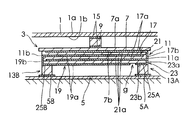
以下、図面を参照して本発明の実施の形態を詳細に説明する。図1は、本発明の一実施の形態のタッチパネルを備えた表示装置の主要部品の配置構成を示す平面図である。図2は、図1のII-II線断面図である。なお、図2では、理解を容易にするため、厚み寸法を誇張して描いている。両図に示すように、本例の表示装置は、タッチパネル1と、2つの圧電アクチュエータ3と、回路基板5とを有している。図1には、タッチパネル1及び回路基板5を収納するケースについては図示していない。タッチパネル1は、透明の板ガラスにより矩形状に形成されている。タッチパネル1の表面には、操作者が指で触れるとオン状態になる透明電極によって形成されたタッチスイッチのスイッチ表示部2が表示されている。なおスイッチ表示部2の詳細は図示していない。
Hereinafter, embodiments of the present invention will be described in detail with reference to the drawings. FIG. 1 is a plan view showing an arrangement configuration of main components of a display device including a touch panel according to an embodiment of the present invention. 2 is a cross-sectional view taken along the line II-II in FIG. In FIG. 2, the thickness dimension is exaggerated for easy understanding. As shown in both drawings, the display device of this example includes a touch panel 1, two piezoelectric actuators 3, and a circuit board 5. FIG. 1 does not show a case for housing the touch panel 1 and the circuit board 5. The touch panel 1 is formed in a rectangular shape by a transparent plate glass. On the surface of the touch panel 1, a switch display unit 2 of a touch switch formed by a transparent electrode that is turned on when an operator touches with a finger is displayed. The details of the switch display unit 2 are not shown.
2つの圧電アクチュエータ3は、タッチパネル1の長手方向の両端部に配置されている。以下、一方の圧電アクチュエータ3について図2を用いてその構造を説明する。圧電アクチュエータ3は、細長いプレート形状を有しており、金属振動板7と、弾性部材9と、圧電素子11と、一対の導電性支持部材13A,13Bとを有している。本例では、圧電アクチュエータ3は、タッチスイッチのスイッチ表示部2に操作者が指で触れたか否かは、前述のスイッチ表示部2を備えるタッチスイッチによって検出される。タッチスイッチがオン状態を検出すると、回路基板5に設けた図示しないアクチュエータ駆動回路から圧電アクチュエータ3に駆動信号(電力)が供給されて、圧電アクチュエータ3は振動する。
The two piezoelectric actuators 3 are arranged at both ends in the longitudinal direction of the touch panel 1. Hereinafter, the structure of one piezoelectric actuator 3 will be described with reference to FIG. The piezoelectric actuator 3 has an elongated plate shape, and includes a metal diaphragm 7, an elastic member 9, a piezoelectric element 11, and a pair of conductive support members 13A and 13B. In this example, the piezoelectric actuator 3 detects whether or not the operator has touched the switch display unit 2 of the touch switch with a finger by the touch switch including the switch display unit 2 described above. When the touch switch detects the ON state, a drive signal (electric power) is supplied from an actuator drive circuit (not shown) provided on the circuit board 5 to the piezoelectric actuator 3, and the piezoelectric actuator 3 vibrates.
金属振動板7は、ステンレス、4-2アロイ等からなり、細長い矩形形状を有している。金属振動板7は、表面7aと裏面7bとを有しており、表面7aがタッチパネル1の裏面1bと弾性部材9を介して対向するように配置されている。本例では、弾性部材9は、弾性を有する合成樹脂材料から形成されている。具体的には、弾性材料として株式会社イノアックから販売されている「PORON・H-48」を用いている。弾性部材9は、後述する一対の入力電極25A,25Bの中間位置に対応する圧電アクチュエータ3の表面部とタッチパネル1の裏面1bとに両面粘着テープ15によりそれぞれ接合されて、圧電アクチュエータ3とタッチパネル1との機械的な連結を図っている。
The metal diaphragm 7 is made of stainless steel, 4-2 alloy, etc., and has an elongated rectangular shape. The metal diaphragm 7 has a front surface 7 a and a back surface 7 b, and is disposed so that the front surface 7 a faces the back surface 1 b of the touch panel 1 with the elastic member 9 interposed therebetween. In this example, the elastic member 9 is formed from a synthetic resin material having elasticity. Specifically, “PORON H-48” sold by Inoac Co., Ltd. is used as an elastic material. The elastic member 9 is bonded to the front surface portion of the piezoelectric actuator 3 corresponding to an intermediate position between a pair of input electrodes 25A and 25B, which will be described later, and the back surface 1b of the touch panel 1 by the double-sided adhesive tape 15, respectively. The mechanical connection with is intended.
圧電素子11は、金属振動板7の裏面7b上に形成されており、第1の導電部17と第2の導電部19と圧電部21と導電接続路23とを有している。第1の導電部17は、2つの第1の導電層17aと、該2つの第1の導電層17aを連結する第1の連結部17bとを有している。2つの第1の導電層17aの内の金属振動板7側に位置する第1の導電層17aは、金属振動板7の裏面7bに接合されている。第2の導電部19も、2つの第2の導電層19aと、該2つの第2の導電層19aを連結する第2の連結部19bとを有している。圧電部21は、圧電セラミックスからなる3つの圧電層21aを含んでいる。1つの圧電層21aは、第1の導電層17aと第2の導電層19aとの間に形成されている。これによって、第1の導電層17aと第2の導電層19aとは圧電層21aを介して対向して配置されている。また、第1及び第2の連結部17b,19bは、圧電素子11の長手方向の両端に位置する第1及び第2の側面11a,11b上にそれぞれ形成されている。
The piezoelectric element 11 is formed on the back surface 7 b of the metal diaphragm 7 and has a first conductive portion 17, a second conductive portion 19, a piezoelectric portion 21, and a conductive connection path 23. The first conductive portion 17 includes two first conductive layers 17a and a first connecting portion 17b that connects the two first conductive layers 17a. The first conductive layer 17 a located on the metal diaphragm 7 side of the two first conductive layers 17 a is bonded to the back surface 7 b of the metal diaphragm 7. The second conductive portion 19 also has two second conductive layers 19a and a second connecting portion 19b that connects the two second conductive layers 19a. The piezoelectric part 21 includes three piezoelectric layers 21a made of piezoelectric ceramics. One piezoelectric layer 21a is formed between the first conductive layer 17a and the second conductive layer 19a. Thus, the first conductive layer 17a and the second conductive layer 19a are arranged to face each other with the piezoelectric layer 21a interposed therebetween. The first and second connecting portions 17b and 19b are formed on the first and second side surfaces 11a and 11b located at both ends in the longitudinal direction of the piezoelectric element 11, respectively.
導電接続路23は、3つの圧電層21aの回路基板5と対向する最外層の圧電層21a(以下、最外圧電層21aと言う)上に形成されており、側面接続路部分23aと対向接続路部分23bとを有している。側面接続路部分23aは、最外圧電層21aの第1の側面11a上に形成されており、端部が第1の導電部17の第1の連結部17bに接続されている。対向接続路部分23bは、側面接続路部分23aに連続して最外圧電層21aの回路基板5と対向する面上に形成されている。対向接続路部分23bと、最外圧電層21a上に形成された第2の導電層19aとの間には、両者が接触しないように間隙gが形成されている。本例では、対向接続路部分23b(導電接続路23の一部)により一対の入力電極25A,25Bの一方の入力電極25Aが構成されており、回路基板5と対向する最外圧電層21a上に形成された第2の導電層19aの対向接続路部分23bから離れた部分(第2の導電部19の一部)により一対の入力電極25A,25Bの他方の入力電極25Bが構成されている。言い換えるならば、圧電素子11の金属振動板7と反対側の部分に一方の入力電極25A(導電接続路23の一部)と、他方の入力電極25B(第2の導電部19の一部)とが形成されている。これにより、第1の導電部17は、一方の入力電極25Aと電気的に接続され、第2の導電部19は、他方の入力電極25Bに電気的に接続される。本例では、第1の導電部17、第2の導電部19及び導電接続路23は、ガラス銀ペーストを用いて印刷により形成されている。圧電層21aは、圧電セラミックスのグリーンシートを焼成して形成されている。グリーンシートを焼成する際に、導電層を形成するガラス銀ペーストの焼成も同時に行われる。複数の導電層と複数の圧電層の焼成は、適宜の順番で行う。そして第1の導電部17の第1の連結部17b、第2の導電部19の第2の連結部19b及び導電接続路23は、全ての導電層と圧電層の焼成が完了した後に形成される。なお、本例では、圧電層21aが3層となっているが、圧電アクチュエータの振幅量を十分に高めるには、圧電層21aが10層以上になるように第1の導電層17aと第2の導電層19aと圧電層21aを積層するのが好ましい。
The conductive connection path 23 is formed on the outermost piezoelectric layer 21a (hereinafter referred to as the outermost piezoelectric layer 21a) facing the circuit board 5 of the three piezoelectric layers 21a, and is connected to the side connection path portion 23a. And a road portion 23b. The side connection path portion 23 a is formed on the first side surface 11 a of the outermost piezoelectric layer 21 a, and the end portion is connected to the first coupling portion 17 b of the first conductive portion 17. The opposing connection path portion 23b is formed on the surface of the outermost piezoelectric layer 21a that faces the circuit board 5 continuously to the side connection path portion 23a. A gap g is formed between the opposing connection path portion 23b and the second conductive layer 19a formed on the outermost piezoelectric layer 21a so that they do not contact each other. In this example, one input electrode 25A of the pair of input electrodes 25A and 25B is configured by the opposing connection path portion 23b (a part of the conductive connection path 23), and on the outermost piezoelectric layer 21a facing the circuit board 5 The other input electrode 25B of the pair of input electrodes 25A and 25B is configured by a portion (a part of the second conductive portion 19) away from the opposing connection path portion 23b of the second conductive layer 19a formed on the second conductive layer 19a. . In other words, one input electrode 25 </ b> A (a part of the conductive connection path 23) and the other input electrode 25 </ b> B (a part of the second conductive part 19) are disposed on the opposite side of the piezoelectric element 11 from the metal diaphragm 7. And are formed. Accordingly, the first conductive portion 17 is electrically connected to one input electrode 25A, and the second conductive portion 19 is electrically connected to the other input electrode 25B. In this example, the 1st electroconductive part 17, the 2nd electroconductive part 19, and the electroconductive connection path 23 are formed by printing using the glass silver paste. The piezoelectric layer 21a is formed by firing a green sheet of piezoelectric ceramic. When the green sheet is fired, the glass silver paste forming the conductive layer is fired at the same time. Firing of the plurality of conductive layers and the plurality of piezoelectric layers is performed in an appropriate order. The first connecting portion 17b of the first conductive portion 17, the second connecting portion 19b of the second conductive portion 19, and the conductive connection path 23 are formed after the baking of all the conductive layers and the piezoelectric layers is completed. The In this example, the piezoelectric layer 21a has three layers. However, in order to sufficiently increase the amplitude of the piezoelectric actuator, the first conductive layer 17a and the second conductive layer 17a are formed so that the piezoelectric layer 21a has ten or more layers. The conductive layer 19a and the piezoelectric layer 21a are preferably laminated.
以上のようにして、各入力電極25A,25Bが形成されることにより、一対の入力電極25A,25Bは、圧電アクチュエータ3の回路基板5と対向する裏面上において、圧電アクチュエータ3の長手方向の両端部にそれぞれ配置されることになる。
As described above, the input electrodes 25A and 25B are formed, so that the pair of input electrodes 25A and 25B are arranged at both ends in the longitudinal direction of the piezoelectric actuator 3 on the back surface facing the circuit board 5 of the piezoelectric actuator 3. It will be arranged in each part.
一対の導電性支持部材13A,13Bは、いずれも直方体形状の導電性フォームによって形成されており、圧電アクチュエータ3と回路基板5との間に配置されている。導電性フォームは、ポリウレタンからなる発泡樹脂内にNiの金属粉が分散して構成されて形成されており、導電性と弾力性の両方の特性を有している。本例では、導電性フォームとしてゴアテックス株式会社のGS8000を用いている。一対の導電性支持部材13A,13Bの一方の導電性支持部材13Aは、一対の入力電極25A,25Bの一方の入力電極25Aと、回路基板5上に設けられた一対の出力電極5A,5Bの一方の出力電極5Aとに導電性を有する導電性感圧接着剤により接続されている。一対の導電性支持部材13A,13Bの他方の導電性支持部材13Bは、一対の入力電極25A,25Bの他方の入力電極25Bと、回路基板5の一対の出力電極5A,5Bの他方の出力電極5Bとに導電性感圧接着剤により接続されている。一対の導電性支持部材13A,13Bは、圧電アクチュエータ3の振動をできるだけ抑制しないように、圧電アクチュエータ3を回路基板5の表面上に支持している。これにより、圧電アクチュエータ3は、回路基板5の表面上に一対の導電性支持部材13A,13Bからなる支持構造を介して支持されることになる。
The pair of conductive support members 13A and 13B are both formed of a rectangular parallelepiped conductive foam, and are disposed between the piezoelectric actuator 3 and the circuit board 5. The conductive foam is formed by dispersing Ni metal powder in a foamed resin made of polyurethane, and has both characteristics of conductivity and elasticity. In this example, GS8000 manufactured by Gore-Tex Corporation is used as the conductive foam. One conductive support member 13A of the pair of conductive support members 13A and 13B includes one input electrode 25A of the pair of input electrodes 25A and 25B and a pair of output electrodes 5A and 5B provided on the circuit board 5. It is connected to one output electrode 5A by a conductive pressure-sensitive adhesive having conductivity. The other conductive support member 13B of the pair of conductive support members 13A and 13B includes the other input electrode 25B of the pair of input electrodes 25A and 25B and the other output electrode of the pair of output electrodes 5A and 5B of the circuit board 5. It is connected to 5B by a conductive pressure sensitive adhesive. The pair of conductive support members 13 </ b> A and 13 </ b> B support the piezoelectric actuator 3 on the surface of the circuit board 5 so as not to suppress the vibration of the piezoelectric actuator 3 as much as possible. As a result, the piezoelectric actuator 3 is supported on the surface of the circuit board 5 via the support structure including the pair of conductive support members 13A and 13B.
本例のタッチパネルを備えた表示装置は、次のように作動する。まず。タッチパネル1のスイッチ表示部2に操作者が指で触れると、図示しないタッチスイッチが接触を検出する。この接触の検出に基づいて、回路基板5上に形成した図示しないアクチュエータ駆動回路から出力電極5A,5Bを介して圧電アクチュエータ3の一対の入力電極25A及び25Bに駆動信号(電力)が供給される。この駆動信号が一対の入力電極入力25A及び25Bに入力されると、圧電アクチュエータ3は、一対の導電性支持部材13A,13Bが節となるような振動をする。その結果、圧電アクチュエータ3の中央部(弾性部材9が配置されている部分)が回路基板5に対して上下運動することになり、タッチパネル1が振動する。これにより、耳や目の不自由な人でも触感により、スイッチが適切に入力されたことを知ることができる。なお圧電アクチュエータの振動時間は、タイマにより定めるようにしてもよいし、タッチスイッチがオン状態になっている間だけ振動させるようにしてもよい。
The display device equipped with the touch panel of this example operates as follows. First. When the operator touches the switch display unit 2 of the touch panel 1 with a finger, a touch switch (not shown) detects contact. Based on this contact detection, a drive signal (electric power) is supplied from a not-shown actuator drive circuit formed on the circuit board 5 to the pair of input electrodes 25A and 25B of the piezoelectric actuator 3 via the output electrodes 5A and 5B. . When this drive signal is input to the pair of input electrode inputs 25A and 25B, the piezoelectric actuator 3 vibrates so that the pair of conductive support members 13A and 13B become nodes. As a result, the central portion of the piezoelectric actuator 3 (the portion where the elastic member 9 is disposed) moves up and down with respect to the circuit board 5, and the touch panel 1 vibrates. As a result, even a person who is blind or visually impaired can know that the switch has been properly input by tactile sensation. The vibration time of the piezoelectric actuator may be determined by a timer, or may be vibrated only while the touch switch is on.
本例のタッチパネルを備えた表示装置では、圧電アクチュエータ3を回路基板5の表面上に支持する支持構造を導電性フォームからなる一対の導電性支持部材13A,13Bによって構成するので、一対の導電性支持部材13A,13Bを備えた圧電アクチュエータ3を回路基板5の所定位置に載置して、一対の導電性支持部材13A,13Bを回路基板5の一対の出力電極5A,5Bに接続するだけで、圧電アクチュエータ3を回路基板5上に実装することができる。そのため、従来のように、圧電アクチュエータの入力電極と、圧電アクチュエータを駆動するアクチュエータ駆動回路の電極とをリード線を用いて配線する必要がなくなり、圧電アクチュエータの取付が容易になる。
In the display device including the touch panel of this example, the support structure for supporting the piezoelectric actuator 3 on the surface of the circuit board 5 is configured by the pair of conductive support members 13A and 13B made of a conductive foam. The piezoelectric actuator 3 provided with the supporting members 13A and 13B is placed at a predetermined position on the circuit board 5, and the pair of conductive supporting members 13A and 13B is simply connected to the pair of output electrodes 5A and 5B on the circuit board 5. The piezoelectric actuator 3 can be mounted on the circuit board 5. Therefore, unlike the prior art, there is no need to wire the input electrode of the piezoelectric actuator and the electrode of the actuator drive circuit for driving the piezoelectric actuator using the lead wires, and the attachment of the piezoelectric actuator becomes easy.
上記実施の形態では、タッチパネルに操作者が指を触れたか否かの検出をタッチパネル上に形成した透明電極からなるタッチスイッチを用いて行っているが、圧電アクチュエータ自身をタッチスイッチとして利用することもできる。この場合には、タッチパネル1が押されたことにより、圧電アクチュエータ内の圧電素子で発生する圧電電圧を検出する検出回路を回路基板5に形成する。そして検出回路の出力でアクチュエータ駆動回路を起動し、アクチュエータ駆動回路から駆動信号を圧電アクチュエータの一対の入力電極に供給する。このようにすると、タッチの検出と振動の発生を圧電アクチュエータを利用して実現できるので部品点数を更に少なくすることができる。
In the above embodiment, whether or not an operator touches the touch panel is detected using a touch switch made of a transparent electrode formed on the touch panel, but the piezoelectric actuator itself may be used as a touch switch. it can. In this case, when the touch panel 1 is pressed, a detection circuit for detecting a piezoelectric voltage generated by the piezoelectric element in the piezoelectric actuator is formed on the circuit board 5. Then, the actuator drive circuit is activated by the output of the detection circuit, and a drive signal is supplied from the actuator drive circuit to the pair of input electrodes of the piezoelectric actuator. In this way, touch detection and vibration generation can be realized by using the piezoelectric actuator, so that the number of parts can be further reduced.
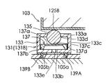
図3は、本発明の他の実施の形態のタッチパネルを備えた表示装置の断面図である。本例の表示装置では、一対の導電性支持部材として導電性フォームの代わりに力センサ(半導体力センサ)を用いている。その他は、図1及び図2に示す実施の形態と同じ構造を有している。そこで、図1及び図2に示す実施の形態と同じ部材には、当該部材に付した符号に100を加えた符号を付して説明を省略する。本例の圧電アクチュエータで用いる一対の導電性支持部材(131)は、操作者の指からタッチパネル101に加わる力の大きさを検知する一対の半導体力センサ131により構成されている。半導体力センサ131は、図4に示すように、ケース133と接触子を構成する導電性を有する球体135と半導体基体137と複数の端子139A,139Bとを有している。ケース133は直方体の箱形を呈しており、圧電素子111と対向する上方壁部133aと、上方壁部133aと対向する下方壁部133bと、上方壁部133aと下方壁部133bとを連結する周壁部133cとを有している。上方壁部133aの中央には上方壁部133aを貫通する円形の開口部133dが形成されており、下方壁部133bの中央には孔部133eが形成されている。接触子を構成する球体135は、導電性を有する金属により形成されている。この球体135は、ケース133の開口部133dから一部分が突出している。開口部133dは球体135の直径より小さい直径寸法を有している。そのため球体135が開口部133dから突出する部分は球体135の半分以下であり、球体135が、開口部133dから抜け出ることはない。一対の半導体力センサ131の一方の半導体力センサ131(131A)の球体135は、一方の入力電極125Aに接触している。また、一対の半導体力センサ131の他方の半導体力センサ131(131B)の球体135は、他方の入力電極125Bに接触している。
FIG. 3 is a cross-sectional view of a display device including a touch panel according to another embodiment of the present invention. In the display device of this example, a force sensor (semiconductor force sensor) is used instead of the conductive foam as the pair of conductive support members. Others have the same structure as the embodiment shown in FIGS. Therefore, the same members as those in the embodiment shown in FIG. 1 and FIG. 2 are denoted by reference numerals obtained by adding 100 to the reference numerals assigned to the members, and description thereof is omitted. The pair of conductive support members (131) used in the piezoelectric actuator of this example includes a pair of semiconductor force sensors 131 that detect the magnitude of the force applied to the touch panel 101 from the operator's finger. As shown in FIG. 4, the semiconductor force sensor 131 includes a conductive sphere 135 that forms a contact with the case 133, a semiconductor base 137, and a plurality of terminals 139A and 139B. The case 133 has a rectangular parallelepiped box shape, and connects the upper wall portion 133a facing the piezoelectric element 111, the lower wall portion 133b facing the upper wall portion 133a, and the upper wall portion 133a and the lower wall portion 133b. And a peripheral wall portion 133c. A circular opening 133d penetrating the upper wall 133a is formed at the center of the upper wall 133a, and a hole 133e is formed at the center of the lower wall 133b. The sphere 135 constituting the contact is made of a conductive metal. A part of the sphere 135 protrudes from the opening 133 d of the case 133. The opening 133 d has a smaller diameter than the diameter of the sphere 135. Therefore, the part where the sphere 135 protrudes from the opening 133d is less than half of the sphere 135, and the sphere 135 does not escape from the opening 133d. The sphere 135 of one semiconductor force sensor 131 (131A) of the pair of semiconductor force sensors 131 is in contact with one input electrode 125A. The sphere 135 of the other semiconductor force sensor 131 (131B) of the pair of semiconductor force sensors 131 is in contact with the other input electrode 125B.
半導体基体137は、ダイヤフラム部137aと、ダイヤフラム部137aの周囲に一体に接続されてダイヤフラム部137aを支持する筒状の支持部137bとを有している。ダイヤフラム部137aの中心には球体135が載置されている。ダイヤフラム部137aには、球体135の変位に応じて撓み且つ撓み量に応じた電気信号を出力する図示しない複数の拡散抵抗が形成されている。また、ダイヤフラム部137a上には、球体135と接触するように接触用電極137cが形成されている。そして、半導体基体137には、接触用電極137cと電気的に接続された配線パターン137dが形成されている。接触用電極137c及び配線パターン137dは、薄膜形成技術を用いて半導体基体137上にアルミニウムや金等の導電性材料により形成されている。本例では、接触用電極137c及び配線パターン137dにより導電路が構成されている。
The semiconductor substrate 137 has a diaphragm portion 137a and a cylindrical support portion 137b that is integrally connected to the periphery of the diaphragm portion 137a and supports the diaphragm portion 137a. A spherical body 135 is placed at the center of the diaphragm portion 137a. The diaphragm portion 137 a is formed with a plurality of diffusion resistors (not shown) that bend according to the displacement of the sphere 135 and output an electrical signal according to the amount of deflection. Further, a contact electrode 137c is formed on the diaphragm portion 137a so as to be in contact with the sphere 135. The semiconductor substrate 137 is provided with a wiring pattern 137d that is electrically connected to the contact electrode 137c. The contact electrode 137c and the wiring pattern 137d are formed of a conductive material such as aluminum or gold on the semiconductor substrate 137 using a thin film formation technique. In this example, a conductive path is constituted by the contact electrode 137c and the wiring pattern 137d.
複数の端子139A,139Bの一部の端子139Aは、配線パターン137dに電気的に接続されている。また残りの一部の端子139Bを含む複数の端子からは、前述したダイヤフラム部137aの撓み量に応じた拡散抵抗の変更を示す電気信号が出力される。端子139Aは、回路基板105のアクチュエータ駆動回路の出力電極105aに半田付け接続されている。また端子139Bを含む複数の出力端子は、回路基板105の複数の検出用電極105bに半田付け接続されている。
Some terminals 139A of the plurality of terminals 139A and 139B are electrically connected to the wiring pattern 137d. In addition, an electrical signal indicating a change in diffusion resistance corresponding to the amount of deflection of the diaphragm portion 137a is output from a plurality of terminals including the remaining part of the terminals 139B. The terminal 139A is soldered to the output electrode 105a of the actuator drive circuit of the circuit board 105. The plurality of output terminals including the terminal 139B are soldered to the plurality of detection electrodes 105b of the circuit board 105.
本例のタッチパネルを備えた表示装置では、タッチパネル101の表面101aに操作者が指で触れると、圧電アクチュエータ103を介して球体135に押圧力が加わる。その結果、半導体力センサ131の端子139Bからは、押圧力の検出に必要な信号が出力され、回路基板105上に設けた図示しない検出回路からは押圧力に応じた検出信号が出力される。また、圧電アクチュエータ103を駆動するアクチュエータ駆動回路は、この検出信号を受信すると、端子139A、半導体力センサ131の配線パターン137dを通して、圧電アクチュエータ103の入力電極125Bに駆動信号を供給する。一方の入力電極125Aにも同様にして半導体力センサ131Aから駆動信号が供給される。その結果、圧電アクチュエータ103が駆動されてタッチパネルが振動する。圧電アクチュエータ103の振動時間については、前の実施の形態と同様に、タイマで定めてもよいし、半導体力センサから検出信号が出力されている期間としてもよい。
In the display device including the touch panel of this example, when an operator touches the surface 101 a of the touch panel 101 with a finger, a pressing force is applied to the sphere 135 via the piezoelectric actuator 103. As a result, a signal necessary for detecting the pressing force is output from the terminal 139B of the semiconductor force sensor 131, and a detection signal corresponding to the pressing force is output from a detection circuit (not shown) provided on the circuit board 105. When the actuator driving circuit that drives the piezoelectric actuator 103 receives this detection signal, the actuator driving circuit supplies the driving signal to the input electrode 125B of the piezoelectric actuator 103 through the terminal 139A and the wiring pattern 137d of the semiconductor force sensor 131. Similarly, a drive signal is supplied to the one input electrode 125A from the semiconductor force sensor 131A. As a result, the piezoelectric actuator 103 is driven and the touch panel vibrates. The vibration time of the piezoelectric actuator 103 may be determined by a timer as in the previous embodiment, or may be a period during which a detection signal is output from the semiconductor force sensor.
本例のタッチパネルを備えた表示装置では、例えば、タッチパネル101に加わる力の大きさを半導体力センサ131によって検知することにより、タッチパネル101に加わる力に応じて表示画面の早送りができる機能を付加することができる。
In the display device including the touch panel of this example, for example, by detecting the magnitude of the force applied to the touch panel 101 by the semiconductor force sensor 131, a function capable of fast-forwarding the display screen according to the force applied to the touch panel 101 is added. be able to.
なお、本例のように一対の導電性支持部材の少なくとも一つを半導体力センサ131によって構成すると、圧電アクチュエータ103が振動する際に半導体力センサ131が圧電アクチュエータ103の振動による力の大きさを検知してしまう。そのため、このような振動による力は、検知しないように(差し引くように)回路基板105の回路は設定されている。
If at least one of the pair of conductive support members is configured by the semiconductor force sensor 131 as in this example, when the piezoelectric actuator 103 vibrates, the semiconductor force sensor 131 determines the magnitude of the force due to the vibration of the piezoelectric actuator 103. It will be detected. Therefore, the circuit of the circuit board 105 is set so as not to detect (subtract) the force caused by such vibration.
また、本例では、一対の導電性支持部材の両方を半導体力センサにより構成したが、一対の導電性支持部材のいずれか一方の導電性支持部材だけを半導体力センサによって構成してもよい。この場合、他方の導電性支持部材は、図1及び図2に示す導電性フォームにより構成すればよい。
In this example, both of the pair of conductive support members are configured by the semiconductor force sensor, but only one of the pair of conductive support members may be configured by the semiconductor force sensor. In this case, what is necessary is just to comprise the other electroconductive support member by the electroconductive foam shown in FIG.1 and FIG.2.
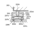
図5は、本発明の更に他の実施の形態のタッチパネルを備えた表示装置の部分断面図である。本例の表示装置は、接触子の構造を除いては、図3及び図4に示す実施の形態と同じ構造を有している。そこで、図3及び図4に示す実施の形態と同じ部材には、当該部材に付した符号に100を加えた符号を付して説明を省略する。本例の表示装置の半導体力センサ231の導電性を有する接触子235は、圧電アクチュエータ203の入力電極(225Aまたは225B)に固定されている。電気的に接続されるように、圧電アクチュエータ203に固定されている。接触子235は、導電性を有する銅により形成されており、円柱部235aと該円柱部235aの端部に形成された半球部235bとを有している。そして、接触子235の半球部235bが位置する側と反対側の一方の端部が半田により入力電極(225Aまたは225B)上に接続されている。そして半球部235bが半導体基体237のダイヤフラム部237aの中心に接触している。
FIG. 5 is a partial cross-sectional view of a display device including a touch panel according to still another embodiment of the present invention. The display device of this example has the same structure as the embodiment shown in FIGS. 3 and 4 except for the structure of the contact. Therefore, the same members as those in the embodiment shown in FIGS. 3 and 4 are denoted by the reference numerals obtained by adding 100 to the reference numerals attached to the members, and the description thereof is omitted. The conductive contact 235 of the semiconductor force sensor 231 of the display device of this example is fixed to the input electrode (225A or 225B) of the piezoelectric actuator 203. The piezoelectric actuator 203 is fixed so as to be electrically connected. The contact 235 is made of conductive copper, and has a cylindrical portion 235a and a hemispherical portion 235b formed at the end of the cylindrical portion 235a. One end of the contact 235 opposite to the side where the hemispherical portion 235b is located is connected to the input electrode (225A or 225B) by soldering. The hemispherical portion 235b is in contact with the center of the diaphragm portion 237a of the semiconductor substrate 237.
本例のタッチパネルを備えた表示装置では、接触子235が圧電アクチュエータ203に固定されているので、半導体力センサ231の接触子235と入力電極(225Aまたは225B)との間で接触不良が発生するのを有効に防ぐことができる。また、接触子235を回路基板205上に配置された半導体力センサ231のケース233に嵌合させるだけで、圧電アクチュエータ203を回路基板205上に間単に位置決めすることができる。
In the display device including the touch panel of this example, since the contact 235 is fixed to the piezoelectric actuator 203, a contact failure occurs between the contact 235 of the semiconductor force sensor 231 and the input electrode (225A or 225B). Can be effectively prevented. Further, the piezoelectric actuator 203 can be simply positioned on the circuit board 205 simply by fitting the contact 235 to the case 233 of the semiconductor force sensor 231 disposed on the circuit board 205.
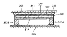
図6は、本発明の更に他の実施の形態のタッチパネルを備えた表示装置の断面図である。本例の表示装置は、圧電アクチュエータとタッチパネルとの接合構造及びタッチパネルの材質を除いて、図1及び図2に示す実施の形態と同じ構造を有している。そこで、図1及び図2に示す実施の形態と同じ部材には、当該部材に付した符号に300を加えた符号を付して説明を省略する。本例の表示装置は、圧電アクチュエータ303とタッチパネル301とが弾性部材を用いずに、接着層341を介して接合されている。また、タッチパネル301は、アクリルからなる合成樹脂により形成されている。
FIG. 6 is a cross-sectional view of a display device including a touch panel according to still another embodiment of the present invention. The display device of this example has the same structure as that of the embodiment shown in FIGS. 1 and 2 except for the joining structure of the piezoelectric actuator and the touch panel and the material of the touch panel. Therefore, the same members as those in the embodiment shown in FIGS. 1 and 2 are denoted by the reference numerals obtained by adding 300 to the reference numerals given to the members, and the description thereof is omitted. In the display device of this example, the piezoelectric actuator 303 and the touch panel 301 are joined via an adhesive layer 341 without using an elastic member. The touch panel 301 is made of a synthetic resin made of acrylic.
本例のタッチパネルを備えた表示装置によれば、圧電アクチュエータ303に生じる撓みがそのまま、タッチパネル301に伝達され、タッチパネル301は、波打つように振動する。そのため、アクリル等の合成樹脂をタッチパネルとして用いた場合でも、タッチパネルを十分に振動させることができる。
According to the display device including the touch panel of this example, the bending generated in the piezoelectric actuator 303 is transmitted as it is to the touch panel 301, and the touch panel 301 vibrates like a wave. Therefore, even when a synthetic resin such as acrylic is used as the touch panel, the touch panel can be sufficiently vibrated.
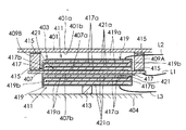
図7は、本発明の更に他の実施の形態のタッチパネルを備えた表示装置の断面図である。なお、図7では、金属振動板407の上方に配置された圧電素子411の厚み寸法を誇張して描いているのに伴って弾性部材409A,409Bの厚み寸法も誇張して描いている。本例の表示装置に用いる圧電アクチュエータ403は、細長いプレート形状を有しており、金属振動板407と、2つの弾性部材409A,409Bと、2つの圧電素子411と、支持部材413からなる支持構造とを有している。圧電アクチュエータ403は、被取付部404上に支持部材413を介して支持されている。
FIG. 7 is a cross-sectional view of a display device including a touch panel according to still another embodiment of the present invention. In FIG. 7, the thickness dimensions of the elastic members 409A and 409B are exaggerated as the thickness dimension of the piezoelectric element 411 disposed above the metal diaphragm 407 is exaggerated. The piezoelectric actuator 403 used in the display device of this example has an elongated plate shape, and includes a support structure including a metal diaphragm 407, two elastic members 409A and 409B, two piezoelectric elements 411, and a support member 413. And have. The piezoelectric actuator 403 is supported on the attached portion 404 via a support member 413.
金属振動板407は、ステンレス、4-2アロイ等からなり、細長い矩形形状を有している。金属振動板407は、表面407aと裏面407bとを有しており、表面407aがタッチパネル401の裏面401bと2つの弾性部材409A,409Bを介して対向するように配置されている。
The metal diaphragm 407 is made of stainless steel, 4-2 alloy, etc., and has an elongated rectangular shape. The metal diaphragm 407 has a front surface 407a and a back surface 407b, and is disposed so that the front surface 407a faces the back surface 401b of the touch panel 401 via two elastic members 409A and 409B.
2つの圧電素子411は、金属振動板407の両面407a,407b上にそれぞれ形成されている。1つの圧電素子411は、第1の導電部417と第2の導電部419と圧電部421とを有している。第1の導電部417は、2つの第1の導電層417aと、該2つの第1の導電層417aを連結する第1の連結部417bとを有している。2つの第1の導電層417aの内の金属振動板407側に位置する第1の導電層417aは、金属振動板407に接合されている。第2の導電部419も、2つの第2の導電層419aと、該2つの第2の導電層419aを連結する第2の連結部419bとを有している。圧電部421は、圧電セラミックスからなる3つの圧電層421aを含んでいる。1つの圧電層421aは、第1の導電層417aと第2の導電層419aとの間に形成されている。これによって、第1の導電層417aと第2の導電層419aとは圧電層421aを介して対向して配置されている。また、第1及び第2の連結部417b,419bは、圧電素子411の長手方向の両端に位置する第1及び第2の側面411a,411b上にそれぞれ形成されている。
The two piezoelectric elements 411 are formed on both surfaces 407a and 407b of the metal diaphragm 407, respectively. One piezoelectric element 411 includes a first conductive portion 417, a second conductive portion 419, and a piezoelectric portion 421. The first conductive portion 417 includes two first conductive layers 417a and a first connecting portion 417b that connects the two first conductive layers 417a. Of the two first conductive layers 417a, the first conductive layer 417a located on the metal diaphragm 407 side is joined to the metal diaphragm 407. The second conductive portion 419 also includes two second conductive layers 419a and a second connecting portion 419b that connects the two second conductive layers 419a. The piezoelectric part 421 includes three piezoelectric layers 421a made of piezoelectric ceramics. One piezoelectric layer 421a is formed between the first conductive layer 417a and the second conductive layer 419a. Thus, the first conductive layer 417a and the second conductive layer 419a are disposed to face each other with the piezoelectric layer 421a interposed therebetween. The first and second connecting portions 417b and 419b are respectively formed on the first and second side surfaces 411a and 411b located at both ends in the longitudinal direction of the piezoelectric element 411.
本例では、第1の導電部417及び第2の導電部419は、ガラス銀ペーストを用いて印刷により形成されている。圧電層421aは、圧電セラミックスのグリーンシートを焼成して形成されている。グリーンシートを焼成する際に、導電層を形成するガラス銀ペーストの焼成も同時に行われる。複数の導電層と複数の圧電層の焼成は、適宜の順番で行う。そして第1の導電部417の第1の連結部417b及び第2の導電部419の第2の連結部419bは、全ての導電層と圧電層の焼成が完了した後に形成される。なお、本例では、圧電層421aが3層となっているが、圧電アクチュエータの振幅量を十分に高めるには、圧電層421aが10層以上になるように第1の導電層417aと第2の導電層419aと圧電層421aを積層するのが好ましい。
In this example, the first conductive portion 417 and the second conductive portion 419 are formed by printing using a glass silver paste. The piezoelectric layer 421a is formed by firing a green sheet of piezoelectric ceramic. When the green sheet is fired, the glass silver paste forming the conductive layer is fired at the same time. Firing of the plurality of conductive layers and the plurality of piezoelectric layers is performed in an appropriate order. The first connecting portion 417b of the first conductive portion 417 and the second connecting portion 419b of the second conductive portion 419 are formed after the baking of all the conductive layers and the piezoelectric layers is completed. In this example, the piezoelectric layer 421a has three layers. However, in order to sufficiently increase the amplitude amount of the piezoelectric actuator, the first conductive layer 417a and the second conductive layer 417a are formed so that the piezoelectric layer 421a has ten or more layers. The conductive layer 419a and the piezoelectric layer 421a are preferably stacked.
弾性部材409A,409Bは、弾性を有する合成樹脂材料から形成されている。具体的には、弾性材料として株式会社イノアックから販売されている「PORON・H-48」を用いている。弾性部材409A,409Bは、圧電アクチュエータ403の長手方向の両端において、圧電アクチュエータ403の表面部(金属振動板407の表面407a)とタッチパネル401の裏面401bとに両面粘着テープ415によりそれぞれ接合されて、圧電アクチュエータ403とタッチパネル401との機械的な連結を図っている。
The elastic members 409A and 409B are made of a synthetic resin material having elasticity. Specifically, “PORON H-48” sold by Inoac Co., Ltd. is used as an elastic material. The elastic members 409A and 409B are bonded to the front surface portion of the piezoelectric actuator 403 (surface 407a of the metal diaphragm 407) and the back surface 401b of the touch panel 401 by double-sided adhesive tape 415 at both ends in the longitudinal direction of the piezoelectric actuator 403, respectively. The piezoelectric actuator 403 and the touch panel 401 are mechanically connected.
支持部材413は、弾性部材409A,409Bと同様の弾性を有する合成樹脂材料によって形成されており、圧電アクチュエータ403の長手方向中央(被取付部404と対向する圧電素子411の長手方向中央)と被取付部404との間に配置されている。支持部材413は、圧電アクチュエータ403の振動をできるだけ抑制しないように、圧電アクチュエータ403を被取付部404の表面上に支持している。これにより、圧電アクチュエータ403は、被取付部404の表面上に支持部材413からなる支持構造を介して支持されることになる。
The support member 413 is made of a synthetic resin material having elasticity similar to that of the elastic members 409A and 409B. The support member 413 has a center in the longitudinal direction of the piezoelectric actuator 403 (a center in the longitudinal direction of the piezoelectric element 411 facing the mounted portion 404). It arrange | positions between the attaching parts 404. FIG. The support member 413 supports the piezoelectric actuator 403 on the surface of the attached portion 404 so as not to suppress the vibration of the piezoelectric actuator 403 as much as possible. As a result, the piezoelectric actuator 403 is supported on the surface of the attached portion 404 via the support structure including the support member 413.
本例の表示装置では、金属振動板407に接続されたリード線L1と、2つの圧電素子411の第2の導電部419にそれぞれ接続されたリード線L2,L3とを用いて所定の配線を行っている。
In the display device of this example, predetermined wiring is performed using the lead wire L1 connected to the metal diaphragm 407 and the lead wires L2 and L3 connected to the second conductive portions 419 of the two piezoelectric elements 411, respectively. Is going.