WO2009128337A1 - Semiconductor device and method for manufacturing the same - Google Patents
Semiconductor device and method for manufacturing the same Download PDFInfo
- Publication number
- WO2009128337A1 WO2009128337A1 PCT/JP2009/056331 JP2009056331W WO2009128337A1 WO 2009128337 A1 WO2009128337 A1 WO 2009128337A1 JP 2009056331 W JP2009056331 W JP 2009056331W WO 2009128337 A1 WO2009128337 A1 WO 2009128337A1
- Authority
- WO
- WIPO (PCT)
- Prior art keywords
- transistor
- gate electrode
- base portion
- local wiring
- type
- Prior art date
Links
- 239000004065 semiconductor Substances 0.000 title claims description 289
- 238000000034 method Methods 0.000 title claims description 61
- 238000004519 manufacturing process Methods 0.000 title claims description 44
- 229910052751 metal Inorganic materials 0.000 claims description 27
- 239000002184 metal Substances 0.000 claims description 27
- 239000007769 metal material Substances 0.000 claims description 13
- 238000000151 deposition Methods 0.000 claims description 7
- 230000008878 coupling Effects 0.000 claims description 5
- 238000010168 coupling process Methods 0.000 claims description 5
- 238000005859 coupling reaction Methods 0.000 claims description 5
- 230000003068 static effect Effects 0.000 claims description 4
- 239000010408 film Substances 0.000 description 47
- 239000000758 substrate Substances 0.000 description 43
- 239000012535 impurity Substances 0.000 description 32
- 239000012212 insulator Substances 0.000 description 30
- 230000008569 process Effects 0.000 description 27
- 238000001459 lithography Methods 0.000 description 22
- 238000003860 storage Methods 0.000 description 20
- 238000009792 diffusion process Methods 0.000 description 19
- 229910021332 silicide Inorganic materials 0.000 description 19
- FVBUAEGBCNSCDD-UHFFFAOYSA-N silicide(4-) Chemical compound [Si-4] FVBUAEGBCNSCDD-UHFFFAOYSA-N 0.000 description 19
- 239000000463 material Substances 0.000 description 14
- 239000010409 thin film Substances 0.000 description 14
- 238000010586 diagram Methods 0.000 description 13
- 230000006870 function Effects 0.000 description 11
- 230000000694 effects Effects 0.000 description 8
- 230000015572 biosynthetic process Effects 0.000 description 7
- 238000005530 etching Methods 0.000 description 7
- 238000002955 isolation Methods 0.000 description 7
- 230000004048 modification Effects 0.000 description 6
- 238000012986 modification Methods 0.000 description 6
- 101100268665 Caenorhabditis elegans acc-1 gene Proteins 0.000 description 5
- 101100268668 Caenorhabditis elegans acc-2 gene Proteins 0.000 description 5
- 230000008901 benefit Effects 0.000 description 5
- 239000004020 conductor Substances 0.000 description 5
- 238000005516 engineering process Methods 0.000 description 5
- 230000010354 integration Effects 0.000 description 5
- 229910052710 silicon Inorganic materials 0.000 description 4
- 229910004298 SiO 2 Inorganic materials 0.000 description 3
- XUIMIQQOPSSXEZ-UHFFFAOYSA-N Silicon Chemical compound [Si] XUIMIQQOPSSXEZ-UHFFFAOYSA-N 0.000 description 3
- 230000008859 change Effects 0.000 description 3
- 230000005669 field effect Effects 0.000 description 3
- 229910021420 polycrystalline silicon Inorganic materials 0.000 description 3
- 229920005591 polysilicon Polymers 0.000 description 3
- 238000012545 processing Methods 0.000 description 3
- 239000010703 silicon Substances 0.000 description 3
- IJGRMHOSHXDMSA-UHFFFAOYSA-N Atomic nitrogen Chemical compound N#N IJGRMHOSHXDMSA-UHFFFAOYSA-N 0.000 description 2
- 229910019001 CoSi Inorganic materials 0.000 description 2
- RYGMFSIKBFXOCR-UHFFFAOYSA-N Copper Chemical compound [Cu] RYGMFSIKBFXOCR-UHFFFAOYSA-N 0.000 description 2
- 229910000577 Silicon-germanium Inorganic materials 0.000 description 2
- 229910052782 aluminium Inorganic materials 0.000 description 2
- XAGFODPZIPBFFR-UHFFFAOYSA-N aluminium Chemical compound [Al] XAGFODPZIPBFFR-UHFFFAOYSA-N 0.000 description 2
- 238000013459 approach Methods 0.000 description 2
- 229910052802 copper Inorganic materials 0.000 description 2
- 239000010949 copper Substances 0.000 description 2
- 229910044991 metal oxide Inorganic materials 0.000 description 2
- 150000004706 metal oxides Chemical class 0.000 description 2
- 229910052914 metal silicate Inorganic materials 0.000 description 2
- 229910052759 nickel Inorganic materials 0.000 description 2
- 230000001681 protective effect Effects 0.000 description 2
- WFKWXMTUELFFGS-UHFFFAOYSA-N tungsten Chemical compound [W] WFKWXMTUELFFGS-UHFFFAOYSA-N 0.000 description 2
- 229910052721 tungsten Inorganic materials 0.000 description 2
- 239000010937 tungsten Substances 0.000 description 2
- VLJQDHDVZJXNQL-UHFFFAOYSA-N 4-methyl-n-(oxomethylidene)benzenesulfonamide Chemical compound CC1=CC=C(S(=O)(=O)N=C=O)C=C1 VLJQDHDVZJXNQL-UHFFFAOYSA-N 0.000 description 1
- ZOXJGFHDIHLPTG-UHFFFAOYSA-N Boron Chemical compound [B] ZOXJGFHDIHLPTG-UHFFFAOYSA-N 0.000 description 1
- 229910019974 CrSi Inorganic materials 0.000 description 1
- 229910003855 HfAlO Inorganic materials 0.000 description 1
- 229910004129 HfSiO Inorganic materials 0.000 description 1
- 229910016006 MoSi Inorganic materials 0.000 description 1
- 229910005883 NiSi Inorganic materials 0.000 description 1
- 229910005881 NiSi 2 Inorganic materials 0.000 description 1
- OAICVXFJPJFONN-UHFFFAOYSA-N Phosphorus Chemical compound [P] OAICVXFJPJFONN-UHFFFAOYSA-N 0.000 description 1
- 229910052581 Si3N4 Inorganic materials 0.000 description 1
- VYPSYNLAJGMNEJ-UHFFFAOYSA-N Silicium dioxide Chemical compound O=[Si]=O VYPSYNLAJGMNEJ-UHFFFAOYSA-N 0.000 description 1
- 229910008484 TiSi Inorganic materials 0.000 description 1
- NRTOMJZYCJJWKI-UHFFFAOYSA-N Titanium nitride Chemical compound [Ti]#N NRTOMJZYCJJWKI-UHFFFAOYSA-N 0.000 description 1
- 229910008812 WSi Inorganic materials 0.000 description 1
- 229910007875 ZrAlO Inorganic materials 0.000 description 1
- 229910006249 ZrSi Inorganic materials 0.000 description 1
- 229910006501 ZrSiO Inorganic materials 0.000 description 1
- -1 ZrSiON Inorganic materials 0.000 description 1
- 238000009825 accumulation Methods 0.000 description 1
- 229910052785 arsenic Inorganic materials 0.000 description 1
- RQNWIZPPADIBDY-UHFFFAOYSA-N arsenic atom Chemical compound [As] RQNWIZPPADIBDY-UHFFFAOYSA-N 0.000 description 1
- QVGXLLKOCUKJST-UHFFFAOYSA-N atomic oxygen Chemical compound [O] QVGXLLKOCUKJST-UHFFFAOYSA-N 0.000 description 1
- 230000004888 barrier function Effects 0.000 description 1
- 229910052796 boron Inorganic materials 0.000 description 1
- 239000000470 constituent Substances 0.000 description 1
- 238000013461 design Methods 0.000 description 1
- 239000007772 electrode material Substances 0.000 description 1
- 238000007667 floating Methods 0.000 description 1
- 229910052735 hafnium Inorganic materials 0.000 description 1
- VBJZVLUMGGDVMO-UHFFFAOYSA-N hafnium atom Chemical compound [Hf] VBJZVLUMGGDVMO-UHFFFAOYSA-N 0.000 description 1
- 230000012447 hatching Effects 0.000 description 1
- 238000010438 heat treatment Methods 0.000 description 1
- 230000006872 improvement Effects 0.000 description 1
- 238000009413 insulation Methods 0.000 description 1
- 238000005468 ion implantation Methods 0.000 description 1
- 230000007257 malfunction Effects 0.000 description 1
- 238000002844 melting Methods 0.000 description 1
- 230000008018 melting Effects 0.000 description 1
- 229910052757 nitrogen Inorganic materials 0.000 description 1
- 230000003647 oxidation Effects 0.000 description 1
- 238000007254 oxidation reaction Methods 0.000 description 1
- 229910052760 oxygen Inorganic materials 0.000 description 1
- 239000001301 oxygen Substances 0.000 description 1
- 229910052698 phosphorus Inorganic materials 0.000 description 1
- 239000011574 phosphorus Substances 0.000 description 1
- 238000009832 plasma treatment Methods 0.000 description 1
- 229910021340 platinum monosilicide Inorganic materials 0.000 description 1
- 230000009467 reduction Effects 0.000 description 1
- 239000003870 refractory metal Substances 0.000 description 1
- 230000007261 regionalization Effects 0.000 description 1
- HQVNEWCFYHHQES-UHFFFAOYSA-N silicon nitride Chemical compound N12[Si]34N5[Si]62N3[Si]51N64 HQVNEWCFYHHQES-UHFFFAOYSA-N 0.000 description 1
- 229910052814 silicon oxide Inorganic materials 0.000 description 1
- 238000009751 slip forming Methods 0.000 description 1
- 239000000126 substance Substances 0.000 description 1
- 238000001947 vapour-phase growth Methods 0.000 description 1
Images


Classifications
-
- H—ELECTRICITY
- H01—ELECTRIC ELEMENTS
- H01L—SEMICONDUCTOR DEVICES NOT COVERED BY CLASS H10
- H01L23/00—Details of semiconductor or other solid state devices
- H01L23/52—Arrangements for conducting electric current within the device in operation from one component to another, i.e. interconnections, e.g. wires, lead frames
- H01L23/535—Arrangements for conducting electric current within the device in operation from one component to another, i.e. interconnections, e.g. wires, lead frames including internal interconnections, e.g. cross-under constructions
-
- H—ELECTRICITY
- H01—ELECTRIC ELEMENTS
- H01L—SEMICONDUCTOR DEVICES NOT COVERED BY CLASS H10
- H01L21/00—Processes or apparatus adapted for the manufacture or treatment of semiconductor or solid state devices or of parts thereof
- H01L21/70—Manufacture or treatment of devices consisting of a plurality of solid state components formed in or on a common substrate or of parts thereof; Manufacture of integrated circuit devices or of parts thereof
- H01L21/71—Manufacture of specific parts of devices defined in group H01L21/70
- H01L21/768—Applying interconnections to be used for carrying current between separate components within a device comprising conductors and dielectrics
- H01L21/76838—Applying interconnections to be used for carrying current between separate components within a device comprising conductors and dielectrics characterised by the formation and the after-treatment of the conductors
- H01L21/76895—Local interconnects; Local pads, as exemplified by patent document EP0896365
-
- H—ELECTRICITY
- H01—ELECTRIC ELEMENTS
- H01L—SEMICONDUCTOR DEVICES NOT COVERED BY CLASS H10
- H01L21/00—Processes or apparatus adapted for the manufacture or treatment of semiconductor or solid state devices or of parts thereof
- H01L21/70—Manufacture or treatment of devices consisting of a plurality of solid state components formed in or on a common substrate or of parts thereof; Manufacture of integrated circuit devices or of parts thereof
- H01L21/77—Manufacture or treatment of devices consisting of a plurality of solid state components or integrated circuits formed in, or on, a common substrate
- H01L21/78—Manufacture or treatment of devices consisting of a plurality of solid state components or integrated circuits formed in, or on, a common substrate with subsequent division of the substrate into plural individual devices
- H01L21/82—Manufacture or treatment of devices consisting of a plurality of solid state components or integrated circuits formed in, or on, a common substrate with subsequent division of the substrate into plural individual devices to produce devices, e.g. integrated circuits, each consisting of a plurality of components
- H01L21/84—Manufacture or treatment of devices consisting of a plurality of solid state components or integrated circuits formed in, or on, a common substrate with subsequent division of the substrate into plural individual devices to produce devices, e.g. integrated circuits, each consisting of a plurality of components the substrate being other than a semiconductor body, e.g. being an insulating body
-
- H—ELECTRICITY
- H01—ELECTRIC ELEMENTS
- H01L—SEMICONDUCTOR DEVICES NOT COVERED BY CLASS H10
- H01L27/00—Devices consisting of a plurality of semiconductor or other solid-state components formed in or on a common substrate
- H01L27/02—Devices consisting of a plurality of semiconductor or other solid-state components formed in or on a common substrate including semiconductor components specially adapted for rectifying, oscillating, amplifying or switching and having potential barriers; including integrated passive circuit elements having potential barriers
- H01L27/12—Devices consisting of a plurality of semiconductor or other solid-state components formed in or on a common substrate including semiconductor components specially adapted for rectifying, oscillating, amplifying or switching and having potential barriers; including integrated passive circuit elements having potential barriers the substrate being other than a semiconductor body, e.g. an insulating body
- H01L27/1203—Devices consisting of a plurality of semiconductor or other solid-state components formed in or on a common substrate including semiconductor components specially adapted for rectifying, oscillating, amplifying or switching and having potential barriers; including integrated passive circuit elements having potential barriers the substrate being other than a semiconductor body, e.g. an insulating body the substrate comprising an insulating body on a semiconductor body, e.g. SOI
-
- H—ELECTRICITY
- H01—ELECTRIC ELEMENTS
- H01L—SEMICONDUCTOR DEVICES NOT COVERED BY CLASS H10
- H01L29/00—Semiconductor devices specially adapted for rectifying, amplifying, oscillating or switching and having potential barriers; Capacitors or resistors having potential barriers, e.g. a PN-junction depletion layer or carrier concentration layer; Details of semiconductor bodies or of electrodes thereof ; Multistep manufacturing processes therefor
- H01L29/40—Electrodes ; Multistep manufacturing processes therefor
- H01L29/41—Electrodes ; Multistep manufacturing processes therefor characterised by their shape, relative sizes or dispositions
- H01L29/423—Electrodes ; Multistep manufacturing processes therefor characterised by their shape, relative sizes or dispositions not carrying the current to be rectified, amplified or switched
- H01L29/42312—Gate electrodes for field effect devices
- H01L29/42316—Gate electrodes for field effect devices for field-effect transistors
- H01L29/4232—Gate electrodes for field effect devices for field-effect transistors with insulated gate
- H01L29/42384—Gate electrodes for field effect devices for field-effect transistors with insulated gate for thin film field effect transistors, e.g. characterised by the thickness or the shape of the insulator or the dimensions, the shape or the lay-out of the conductor
- H01L29/42392—Gate electrodes for field effect devices for field-effect transistors with insulated gate for thin film field effect transistors, e.g. characterised by the thickness or the shape of the insulator or the dimensions, the shape or the lay-out of the conductor fully surrounding the channel, e.g. gate-all-around
-
- H—ELECTRICITY
- H01—ELECTRIC ELEMENTS
- H01L—SEMICONDUCTOR DEVICES NOT COVERED BY CLASS H10
- H01L29/00—Semiconductor devices specially adapted for rectifying, amplifying, oscillating or switching and having potential barriers; Capacitors or resistors having potential barriers, e.g. a PN-junction depletion layer or carrier concentration layer; Details of semiconductor bodies or of electrodes thereof ; Multistep manufacturing processes therefor
- H01L29/66—Types of semiconductor device ; Multistep manufacturing processes therefor
- H01L29/68—Types of semiconductor device ; Multistep manufacturing processes therefor controllable by only the electric current supplied, or only the electric potential applied, to an electrode which does not carry the current to be rectified, amplified or switched
- H01L29/76—Unipolar devices, e.g. field effect transistors
- H01L29/772—Field effect transistors
- H01L29/78—Field effect transistors with field effect produced by an insulated gate
- H01L29/786—Thin film transistors, i.e. transistors with a channel being at least partly a thin film
- H01L29/78642—Vertical transistors
-
- H—ELECTRICITY
- H10—SEMICONDUCTOR DEVICES; ELECTRIC SOLID-STATE DEVICES NOT OTHERWISE PROVIDED FOR
- H10B—ELECTRONIC MEMORY DEVICES
- H10B10/00—Static random access memory [SRAM] devices
-
- H—ELECTRICITY
- H10—SEMICONDUCTOR DEVICES; ELECTRIC SOLID-STATE DEVICES NOT OTHERWISE PROVIDED FOR
- H10B—ELECTRONIC MEMORY DEVICES
- H10B10/00—Static random access memory [SRAM] devices
- H10B10/12—Static random access memory [SRAM] devices comprising a MOSFET load element
- H10B10/125—Static random access memory [SRAM] devices comprising a MOSFET load element the MOSFET being a thin film transistor [TFT]
-
- H—ELECTRICITY
- H01—ELECTRIC ELEMENTS
- H01L—SEMICONDUCTOR DEVICES NOT COVERED BY CLASS H10
- H01L29/00—Semiconductor devices specially adapted for rectifying, amplifying, oscillating or switching and having potential barriers; Capacitors or resistors having potential barriers, e.g. a PN-junction depletion layer or carrier concentration layer; Details of semiconductor bodies or of electrodes thereof ; Multistep manufacturing processes therefor
- H01L29/66—Types of semiconductor device ; Multistep manufacturing processes therefor
- H01L29/68—Types of semiconductor device ; Multistep manufacturing processes therefor controllable by only the electric current supplied, or only the electric potential applied, to an electrode which does not carry the current to be rectified, amplified or switched
- H01L29/76—Unipolar devices, e.g. field effect transistors
- H01L29/772—Field effect transistors
- H01L29/78—Field effect transistors with field effect produced by an insulated gate
- H01L29/7827—Vertical transistors
-
- H—ELECTRICITY
- H01—ELECTRIC ELEMENTS
- H01L—SEMICONDUCTOR DEVICES NOT COVERED BY CLASS H10
- H01L2924/00—Indexing scheme for arrangements or methods for connecting or disconnecting semiconductor or solid-state bodies as covered by H01L24/00
- H01L2924/0001—Technical content checked by a classifier
- H01L2924/0002—Not covered by any one of groups H01L24/00, H01L24/00 and H01L2224/00
-
- H—ELECTRICITY
- H10—SEMICONDUCTOR DEVICES; ELECTRIC SOLID-STATE DEVICES NOT OTHERWISE PROVIDED FOR
- H10B—ELECTRONIC MEMORY DEVICES
- H10B10/00—Static random access memory [SRAM] devices
- H10B10/12—Static random access memory [SRAM] devices comprising a MOSFET load element
Definitions
- the present invention relates to a semiconductor device having local wiring with a special structure and a method for manufacturing the same.
- a semiconductor device including a plurality of MIS field effect transistors (hereinafter sometimes simply referred to as “transistors”) has been used.
- miniaturization is demanded, and improvement in integration and performance have been realized simultaneously by miniaturization of transistor dimensions.
- miniaturization has progressed drastically, and miniaturization has progressed to such a level that the gate insulating film thickness of a transistor is 2 nm or less and the gate length is 50 nm or less. Therefore, it is becoming difficult to advance the miniaturization by simply reducing the dimensions of each part of the transistor for reasons such as an increase in leakage current and an increase in characteristic variation.
- the related planar transistor in which a channel region is formed in the vicinity of the surface of the substrate has a large occupation area, and thus there is a limit to miniaturization.
- a technique using a so-called vertical transistor having a lower impurity diffusion region, a semiconductor region, and an upper impurity diffusion region in this order has been studied.
- a channel current flows parallel to the surface direction of the substrate.
- this vertical transistor has a feature that a channel current flows in a direction (vertical direction) perpendicular to the substrate surface. Further, the vertical transistor has an advantage that the occupied area can be reduced as compared with the planar transistor.
- JP-A-06-066941, JP-A-07-099311, JP-A-08-088328, JP-A-09-232447, JP-A-10-077942, and JP-A-2003-224211 A semiconductor device including a vertical transistor is disclosed.
- a wiring layer made of a low-resistance metal such as aluminum or copper is generally disposed above the transistor.
- a wiring layer made of a low-resistance metal such as aluminum or copper is generally disposed above the transistor.
- high-temperature treatment is performed in the transistor formation process, so that when a transistor is formed after the formation of the wiring layer, the low-resistance metal constituting the wiring layer cannot withstand the high temperature at the time of transistor formation and deteriorates. . For this reason, it is necessary to form a wiring layer after forming the transistor.
- the source, drain, and gate electrode are electrically connected to the upper wiring layer through contact plugs extending in the direction perpendicular to the surface direction of the substrate.
- either one of the source and the drain is positioned below as a lower impurity diffusion region due to the structure. Therefore, there arises a problem of how to electrically connect the lower impurity diffusion region and the wiring above the transistor.
- a contact plug cannot be provided directly above the lower impurity diffusion region and electrically connected to the upper wiring layer.
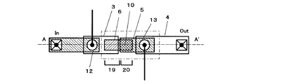
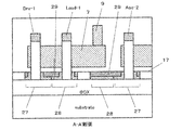
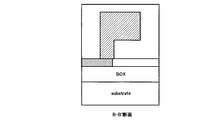
- FIGS. 1A and 1B are a top view showing a connection portion between a lower impurity diffusion region and a wiring layer
- FIG. 1B is a cross-sectional view taken along the line A-A ′ of FIG. 1A.
- the lower impurity diffusion region can be extended in the surface direction of the substrate, and the extended portion can be electrically connected to the upper wiring layer via the contact plug.
- this method is used, an extra area for electrically connecting the lower impurity diffusion region with the contact plug is required. For this reason, the occupied area becomes large, which may be disadvantageous in miniaturization.
- FIGS. 1C and 1D Another method for electrically connecting the lower impurity diffusion region and the wiring layer is shown in FIGS. 1C and 1D.
- FIG. 1C is a top view showing a connection portion between the lower impurity diffusion region and the wiring layer
- FIG. 1D is a cross-sectional view taken along the line A-A ′ of FIG. 1C.
- another method is to place the wiring layer below the vertical transistor.
- vertical transistors are disclosed in this manner.
- the wiring layer disposed below the vertical transistor is exposed to a high temperature in the process of forming the vertical transistor. Therefore, it is necessary to use a material that can be used at a high temperature such as a refractory metal or silicon as a material for the wiring layer.
- a material that can be used at a high temperature such as a refractory metal or silicon
- the wiring resistance is significantly increased as compared with an aluminum or copper wiring layer.
- the present invention has been made in view of the above problems, and an object of the present invention is to provide a miniaturized semiconductor device by reducing the area occupied by wirings that electrically connect vertical transistors.
- a semiconductor device comprising at least first and second transistors and a first local wiring
- the first and second transistors are: A pillar portion made of a semiconductor protruding from the surface of the base portion; A lower conductive region serving as one of a source and a drain provided in the base portion; An upper conductive region serving as the other of the source and the drain provided on the upper part of the column part; A gate electrode provided on a side surface of the column part; A gate insulating film interposed between the gate electrode and the pillar portion;
- the first local wiring is Convex portions protruding from the surface of the base portion; A protrusion protruding from the side surface of the protrusion; With The convex portion of the first local wiring is connected to the lower conductive region of the first transistor, The protruding portion of the first local wiring is connected to the gate electrode of the second transistor,
- the lower surface of the protruding portion of the first local wiring is disposed at a height equal to or lower than the upper surface of the gate electrode of the
- a method of manufacturing a semiconductor device including at least first and second transistors and a first local wiring, (1) a pillar portion made of a semiconductor protruding from the surface of the base portion; A lower conductive region serving as one of a source and a drain provided in the base portion; An upper conductive region serving as the other of the source and the drain provided on the upper part of the column part; A gate electrode provided on a side surface of the column part; A gate insulating film interposed between the gate electrode and the pillar portion; Forming first and second transistors comprising: (2) a convex portion protruding from the surface of the base portion; A protrusion protruding from the side surface of the protrusion; With The convex portion is connected to the lower conductive region of the first transistor, The protrusion is connected to the gate electrode of the second transistor; Forming a first local wiring in which the lower surface of the protruding portion is disposed at a height below the upper surface of the gate electrode of the second transistor;
- the lower surface of the protruding portion of the first local wiring is disposed at a height below the upper surface of the gate electrode of the second transistor. For this reason, it is possible to increase the density as compared with the case of using a wiring whose lower surface is higher than the upper surface of the gate electrode.
- the first local wiring can be formed by a single lithography process except when it is necessary to insulate the lower conductive region below the gate electrode from the first local wiring.
- the height of the first local wiring can be reduced, an increase in the height of the upper wiring due to the use of the first local wiring can be suppressed.
- Acc-1, Acc-2 Access transistor Drv-1, Drv-2: Driver transistor Load-1, Load-2: Load transistor nSD: N-type source and drain pSD: P-type source and drain STI: Device Isolation insulator LI: Wiring IC: Wiring BOX: Embedded insulator SD1 First connection base portion SD2 Second connection base portion Gate Gate electrode 1 First inverter 2 Second inverters 3, 4, 14 Lower conductive region, connection Base part 5 Second connecting gate electrode 7 First connecting gate electrode 6 First local wiring 8 Contact plugs 9, 13 Wirings 11a, 11b Third inverter 12 First transistor 13 Second transistor 14 Substrate 15 Gate electrode Upper surface 17 Base portion surface 18 Column portion 19 Protruding portion 20 Protruding portion 21 Upper conductive region 22 Lower surface 23 of local wiring Upper surface 27 of local wiring First conductive type semiconductor region 28 Second conductive type semiconductor region 29 Silicide layer
- the semiconductor device has a first transistor, a second transistor, and a first local wiring.
- the first and second transistors are provided on a pillar portion made of a semiconductor projecting from the surface of the base portion, a lower conductive region serving as one of a source and a drain provided on the base portion, and an upper portion of the pillar portion.
- a field effect transistor having an upper conductive region which is the other of a source and a drain, a gate electrode provided on a side surface of a column part, and a gate insulating film interposed between the gate electrode and the column part.
- the first and second transistors are formed on the same surface.
- the “base portion” represents a specific region in the substrate including at least a part of the lower conductive region of each transistor.
- the base portion may be provided as a single region for each transistor or may be provided as a connecting base portion common to a plurality of transistors.
- the first local wiring electrically connects the lower conductive region of the first transistor and the gate electrode of the second transistor directly.
- the first local wiring includes a protruding portion protruding from the base portion and a protruding portion protruding from the side surface of the protruding portion.
- the projecting portion is connected to the lower conductive region of the first transistor, and the projecting portion is connected to the gate electrode of the second transistor.
- the lower surface of the protruding portion of the first local wiring is disposed at a height that is lower than the upper surface of the gate electrode of the second transistor. That is, the lower surface is located at a height between the height of the upper surface of the gate electrode with which the protruding portion contacts and the surface of the base portion.
- the first local wiring is (a) a point where the lower conductive region of the transistor is directly electrically connected to the gate electrode, and (b) the protruding portion is disposed at a height below the upper surface of the gate electrode. It is distinguished from a wiring structure that is electrically connected through a contact plug and an upper wiring in that it has a lower surface. The above definition is the same for the second local wiring and the third local wiring described later.
- a step portion is generated at the boundary portion where the “first local wiring”, “second local wiring”, and “third local wiring” are electrically connected to the gate electrode. . Therefore, for example, in this boundary portion, the gate electrode and the wiring overlap in FIGS. 4A, 5, 6 A, 7 to 9, 11 A, 19 A, 23 A, 23 B, 24 A, 24 B, 27, 30 A, 30 B, 31 and 33. (In some drawings, this overlapping portion is indicated by reference numeral 10).
- the top surfaces of these local wirings may be the same height as the top surface of the gate electrode or may have a different height.
- the protruding portions of “first local wiring”, “second local wiring”, and “third local wiring” have two lower surfaces with different heights even if they have one lower surface. May be.
- the lower surface of the protruding portion is disposed at a height equal to or lower than the upper surface of the gate electrode”.
- At least one lower surface of the protrusion is disposed at a height equal to or lower than at least one upper surface of the gate electrode.
- all the lower surfaces of the protrusions are arranged at a height equal to or lower than the upper surface (the upper surface having the shortest distance to the substrate surface) located on the surface of the gate electrode.
- the lower conductive region” and the “upper conductive region” constitute the source and drain of each transistor.
- the lower conductive region may be a source and the upper conductive region may be a drain, the upper conductive region may be a source, and the lower conductive region may be a drain.
- the lower conductive region is a semiconductor or conductive region.
- the lower conductive region is made of a semiconductor containing impurities.
- the entire lower conductive region may be made of a metal material (a metal material is generally a material whose resistance increases as the temperature increases). Note that when the entire lower conductive region of the transistor is made of metal, the transistor has a so-called metal source and drain.
- the semiconductor device can reduce the area occupied by the electrical connection portion as compared with the case where the lower conductive region of the first transistor and the gate electrode of the second transistor are connected by the contact plug and the upper layer wiring. .
- the lower surface of the first local wiring is positioned between the height of the upper surface of the gate electrode with which the protruding portion contacts and the surface of the base portion. For this reason, it is possible to increase the density as compared with the case of using a wiring whose lower surface is higher than the upper surface of the gate electrode. Except when it is necessary to insulate the lower conductive region below the gate electrode from the first local wiring, the first local wiring can be formed by one lithography process. In addition, since the height of the first local wiring can be reduced, an increase in the height of the upper wiring due to the use of the first local wiring can be suppressed.
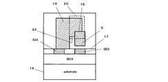
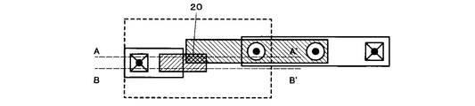
- 35 to 37, 39, and 40 show an example of the semiconductor device of the present invention.
- 35A is a top view of the semiconductor device
- FIGS. 35B, 36A, 36B, 37A, and 37B are A-A ′ cross-sectional views of a portion surrounded by a dotted line in the semiconductor device of FIG. 35A.
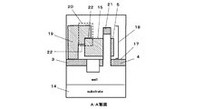
- this semiconductor device includes a first transistor 12 and a second transistor 13.
- the lower conductive region 3 of the first transistor 12 is electrically connected to the gate electrode 5 of the second transistor 13 by the first local wiring 6.
- the first and second transistors have a column portion 18 made of a semiconductor protruding from the base portion surface 17.
- the gate electrode 5 of the second transistor 13 has an upper surface 15 facing in the same direction as the base body surface 17 of the second transistor 13.
- the first local wiring 6 has a protrusion 19 that contacts the lower conductive region 3 of the first transistor, and a protrusion 20 that protrudes from the side surface of the protrusion 19 and contacts the gate electrode 5 of the second transistor (FIG. And a portion surrounded by a dotted line in 35B).
- the protruding portion 20 has a lower surface facing the base portion surface 17.
- this lower surface is in contact with the upper surface of the gate electrode 5 and has the same height as the upper surface.
- the side surface of the gate electrode 5 is in contact with the side surface of the convex portion 19.
- the lower surface of the protruding portion 20 of the first local wiring is disposed at a height equal to or lower than the upper surface 15 of the gate electrode 5 with which the protruding portion contacts. That is, the lower surface of the protruding portion 20 is positioned at a height between the height of the upper surface 15 of the gate electrode 5 and the surface 17 of the base portion. There may be one or a plurality of lower surfaces.
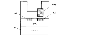
- FIG. 36A shows a semiconductor device in which the side surface of the convex portion 19 of the first local wiring is not in contact with the side surface of the gate electrode 5 and only the lower surface 22 of the first local wiring is in contact with the upper surface 15 of the gate electrode 5. Yes.
- the lower surface 22 has the same height as the upper surface 15 of the gate electrode 5.
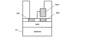
- FIG. 37A shows a semiconductor device in which the protruding portion 20 of the first local wiring has two lower surfaces 22, and one of the lower surfaces 22 is in contact with the upper surface 15 of the gate electrode 5.
- one of the lower surfaces 22 has the same height as the upper surface 15 of the gate electrode 5.
- the other of the lower surface 22 is lower than the upper surface 15 of the gate electrode 5 and is located on the substrate surface 17 side.
- the side surface of the convex portion 19 of the first local wiring and the lower surface 22 of the protruding portion 20 are in contact with the gate electrode 5, but the first local wiring is entirely lower than the upper surface 15 of the gate electrode 5.
- the semiconductor device which exists in the part surface 17 side is represented.
- the lower surface 22 is disposed on the base portion surface 17 side which is lower than the upper surface 15 of the gate electrode 5.
- the upper surface 23 of the first local wiring is also disposed on the base portion surface 17 side, which is lower than the upper surface 15 of the gate electrode 5.
- FIG. 39 is a diagram showing another example of the semiconductor device of the present invention.
- 39A is a top view of the semiconductor device
- FIGS. 39B and 39C are A-A ′ sectional view and B-B ′ sectional view of the semiconductor device of FIG. 39A, respectively.
- the contact portion between the first local wiring and the gate electrode partially overlaps. That is, the first local wiring is in contact with the gate electrode at a position different from that directly above the base portion, and the first local wiring is formed by one lithography process.
- the contact plug connected to the left base portion and the column portion of the transistor belonging to the right base portion are omitted. As shown in FIG.
- FIG. 40 is a diagram showing another example of the semiconductor device of the present invention.
- 40A is a top view of the semiconductor device
- FIGS. 40B and 40C are A-A ′ sectional view and B-B ′ sectional view of the semiconductor device of FIG. 40A, respectively.
- the first local wiring is in contact with the gate electrode at a position immediately above the base portion, and the first local wiring is formed by two lithography processes to separate the first local wiring from the base portion immediately below the gate electrode. Yes.
- contact plugs connected to the left base portion and transistor column portions belonging to the right base portion are omitted. As shown in FIG.
- a region where the right-side base portion and the local wiring overlap each other corresponds to the protruding portion as viewed from above (20 in FIGS. 40A and B). This region is defined by one of two lithography processes. In FIG. 40B, the column portion is omitted.
- the first and second transistors may be n-type transistors or p-type transistors.
- the first and second transistors may be transistors of the same conductivity type or may be transistors of different conductivity types.
- the convex portion, the protruding portion, the lower surface, and the like of the first local wiring have been described.
- the second and third local wirings are also referred to as the first local wiring.
- it has a convex part, a protrusion part, and a lower surface.
- the lower surfaces of the protrusions of the second and third local wirings are arranged at a height that is lower than the upper surface of the gate electrode to which the protrusions are connected.
- the second and third local wirings can have the same effect as the first local wiring.
- Inverter Chain An embodiment of the present invention relates to an inverter chain.
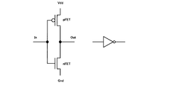
- This inverter chain is formed by connecting a plurality of inverters shown in FIG. 2 as shown in FIG. 3, and can be used as a buffer or a delay element.
- each inverter is composed of a p-type vertical transistor and an n-type vertical transistor.
- Each vertical transistor includes a column portion, a lower conductive region that is one of a source and a drain provided in the base portion, an upper conductive region that is the other of the source and drain provided in the upper portion of the column portion,
- This is a field effect transistor having a gate electrode provided on the side surface of the part and a gate insulating film interposed between the gate electrode and the column part.
- the gate electrodes of the vertical transistors constituting each inverter are shared and integrally formed as a connection gate electrode. By integrating the gate electrodes in this way to form a connection gate electrode, it is possible to increase the density.
- the lower conductive regions of the first and third transistors and the second connection gate electrode are electrically connected by the first local wiring.
- the lower surface of the protruding portion of the first local wiring is disposed at a height that is lower than the upper surface of the second connection gate electrode.
- the lower conductive regions of the second and fourth transistors and the third connection gate electrode are electrically connected by the second local wiring.
- the lower surface of the protruding portion of the second local wiring is disposed at a height that is lower than the upper surface of the third connection gate electrode.
- the first to sixth transistors are formed on the same surface.
- the lower conductive region may be any region of the source and the drain.
- the upper conductive region may be any region of the source and the drain as long as it is a region different from the lower conductive region.
- the constituent material of the gate insulating film is not particularly limited.
- a metal oxide, a metal silicate, a metal oxide, or a high dielectric constant insulating film in which nitrogen is introduced into a metal silicate can be used.
- the “high dielectric constant insulating film” refers to an insulating film having a relative dielectric constant (about 3.6 in the case of SiO 2 ) larger than SiO 2 widely used as a gate insulating film in a semiconductor device.
- the dielectric constant of the high dielectric constant insulating film can be from ten to several thousand.
- the high dielectric constant insulating film for example, HfSiO, HfSiON, HfZrSiO, HfZrSiON, ZrSiO, ZrSiON, HfAlO, HfAlON, HfZrAlO, HfZrAlON, ZrAlO, ZrAlON, or the like can be used.
- the gate electrode can be composed of, for example, conductive polysilicon, metal, silicide, or a laminate thereof.
- the conductive polysilicon can be obtained, for example, by incorporating impurities into the polysilicon.
- the impurity concentration is preferably in the range of 1.0 ⁇ 10 20 to 1.0 ⁇ 10 21 / cm 3 .
- the impurity include phosphorus, arsenic, and boron.
- the same metal material as the material of the gate electrode.
- it can manufacture easily by making a gate electrode into the same metal material.
- different materials are used for the n-type vertical transistor gate electrode and the p-type vertical transistor gate electrode constituting the same inverter. Also good.
- Silicide can also be used as a material for the gate electrode.
- Specific examples of the silicide include NiSi, Ni 2 Si, Ni 3 Si, NiSi 2 , WSi, TiSi 2 , VSi 2 , CrSi 2 , ZrSi 2 , NbSi 2 , MoSi 2 , TaSi 2 , CoSi, CoSi 2 , PtSi, Pt 2 Si, and the like Pd 2 Si.
- the n-type and p-type transistors are electrically connected.
- Each of the p-type transistors can take various arrangements. In the following, a specific arrangement of each transistor and a wiring structure for electrically connecting the respective inverters will be described by way of examples. The following examples are presented for easy understanding of the present invention, and the present invention is not limited to the following examples.
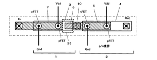
- FIG. 4A is a top view showing a two-stage inverter chain including the first inverter 1 and the second inverter 2 in the present embodiment.
- the first inverter 1 includes a first n-type transistor (nFET) (corresponding to a first transistor) and a first p-type transistor (pFET) (corresponding to a third transistor).
- the second inverter 2 includes a second n-type transistor (nFET) (corresponding to the second transistor) and a second p-type transistor (pFET) (corresponding to the fourth transistor). ing.
- the gate electrodes of the first n-type transistor and the first p-type transistor are connected to form a first connection gate electrode.
- the gate electrodes of the second n-type transistor and the second p-type transistor are connected to form a second connection gate electrode.
- the direction from the first n-type transistor toward the first p-type transistor is parallel to the direction from the second n-type transistor toward the second p-type transistor.
- the lower conductive region 3 of the n-type transistor (nFET) constituting the first inverter 1 and the lower conductive region 3 of the p-type transistor (pFET) are separated from each other. Not adjacent. Further, the lower conductive region 3 of the n-type transistor, the lower conductive region 3 of the p-type transistor, and the second connection gate electrode 5 constituting the first inverter are electrically connected via the first local wiring 6. Connected.
- the first local wiring 6 and the second connection gate electrode 5 are formed by extending the first local wiring in FIG. 4A and an extension of the gate electrode 5 (the gate electrode extends to a region other than above the lower conductive region).
- the portion 10 is electrically connected at the overlapping portion 10.
- the lower surface of the protruding portion of the first local wiring faces the surface of the base portion and is disposed at a height equal to or lower than the upper surface of the second connection gate electrode. That is, the lower surface of the protruding portion of the first local wiring is positioned at a height between the height of the upper surface of the second connection gate electrode 5 and the surface of the base portion.
- the square represents the position of the contact hole, and the contact plug electrically connected to the upper conductive region of the transistor is not shown, and only “ ⁇ ” indicates that there is an electrical connection. .
- the first connection gate electrode 7 and the upper conductive region 8 of each transistor are electrically connected to external wiring via a contact plug.
- the lower conductive region 4 of the n-type and p-type transistors of the second inverter is electrically connected to the external wiring via the wiring 21 and the contact plug.
- FIG. 4B is a diagram illustrating an example in which the same electrical connection between the inverters as in FIG. 4A is realized by a normal contact plug and an upper layer wiring without using the first local wiring.
- the occupation area of this arrangement is 44F 2 in an ideal case.
- the contact hole and the wiring are formed by separate lithography processes.
- the first local wiring can be formed by one lithography process, the number of wiring forming processes can be minimized.
- the lower surface of the protruding portion of the first local wiring 6 is positioned at a height equal to or lower than the upper surface of the connection gate electrode 5. is doing.
- the first local wiring preferably has a structure in contact with at least a part of the side surface of the connection gate electrode 5 in order to reduce contact resistance. In order to obtain this advantage, the first local wiring is not applied to the wiring that intersects the connection gate electrode 5 without contacting the connection gate electrode 5.
- the distance from the lower conductive region to the upper wiring tends to be longer than that of a normal planar transistor.
- the use of the first local wiring increases the height of the upper wiring (the upper wiring has a certain distance from the local wiring). Can be suppressed as compared to the case of a planar transistor.
- the local wiring includes the function of connecting the output of the inverter to the input of the next-stage inverter, and the lower conductive region of the n-type transistor and the lower conductive region of the p-type transistor that are separated from each other. Plays an electrical connection function. That is, two functions are realized simultaneously while preventing an increase in area.
- FIG. 5 is a top view showing a four-stage inverter chain including the first inverter 1, the second inverter 2, and the two third inverters 11a and 11b.
- Each of the third inverters 11a and 11b includes a third n-type transistor (nFET) (corresponding to a fifth transistor) and a third p-type transistor (pFET) (corresponding to a sixth transistor).
- nFET n-type transistor
- pFET third p-type transistor
- the pillars, upper conductive region, lower conductive region, gate electrode and gate insulating film of the fifth and sixth transistors have the same structure as the first to fourth transistors.
- the gate electrodes of the third n-type transistor and the third p-type transistor are connected to form a third connection gate electrode.
- a wiring 21 that electrically connects the lower conductive regions 4 of the n-type and p-type transistors constituting the second inverter 2 (this wiring 21 is formed simultaneously with the first local wiring. However, it was electrically connected to external wiring via a contact plug. However, in this embodiment, the lower conductive region 4 of the n-type and p-type transistors is further electrically connected to the third connection gate electrode 12 constituting the third inverter 11a by the second local wiring 9. This is different from the first embodiment. Similarly, the third inverter 11 a and the third inverter 11 b are electrically connected via the second local wiring 9. Similar to the first local wiring 6, the second local wiring 9 has a convex portion and a protruding portion.
- the lower surface of the projecting portion is disposed at a height equal to or lower than the upper surface of the third connection gate electrode. That is, the lower surface of the protrusion is opposed to the surface of the base portion and is located at a height between the height of the upper surface of the gate electrode 5 and the surface of the base portion. Further, the lower conductive region 14 of the n-type and p-type transistors constituting the third inverter 11b is electrically connected to the external wiring via the wiring 13 and the contact plug.
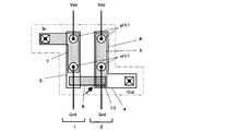
- FIG. 6A is a top view showing a two-stage inverter chain having a different transistor arrangement from that of the first embodiment.
- the lower conductive region of the first n-type transistor (nFET) constituting the first inverter 1 and the lower conductive region of the first p-type transistor (pFET) are connected and integrated.
- the first connection base 3 is formed.
- These lower conductive regions are electrically connected to the lower conductive region by a silicide layer provided by salicide technology.
- the lower conductive region of the second n-type transistor (nFET) constituting the second inverter 2 and the lower conductive region of the second p-type transistor (pFET) are connected and integrated.
- the second connecting base portion 4 is formed. These lower conductive regions are electrically connected to the lower conductive region by a silicide layer provided by salicide technology.
- the first connection base portion 3 includes a first conductivity type semiconductor region 27 and a second conductivity type semiconductor region 28 joined to the first conductivity type semiconductor region 27.
- the first and second conductive semiconductor regions 27 and 28 form a two-dimensional planar region when viewed from above (in the normal direction of the substrate surface).
- the first conductive type semiconductor region 27 is provided with a column portion of the first n-type transistor.
- the second conductive semiconductor region 28 is provided with a column portion of the first p-type transistor.
- the second connection base portion similarly to the first connection base portion, the second connection base portion includes a first conductive type semiconductor region, a second conductive type semiconductor region, and a silicide layer, and the first and second conductive base portions are provided.
- the type semiconductor regions are electrically connected.
- the area can be further reduced by using the first connection base portion in which the n-type and p-type lower conductive regions are connected and integrated.
- connection means of the lower conductive region 3 of the n-type and p-type transistors is not limited to the silicide layer.
- each lower conductive region 3 is made of a metal material, whereby the adjacent lower conductive regions 3 can be electrically connected.
- the first connection base 3 has a first base extension 23 extending in a direction from one of the first n-type transistor and the first p-type transistor to the other.
- the convex portion of the first local wiring 6 is connected to the first base body extension portion 23.
- connection portion between the first local wiring 6 and the connection gate electrode 5 is represented by a portion 10 where the first local wiring and the connection gate electrode overlap in FIG. 6A.
- the protruding portion of the first local wiring is connected between the second connection gate electrode, the column portion of the second n-type transistor, and the column portion of the second p-type transistor.
- the first local wiring is insulated from the second connecting base portion. 6A, as in FIG. 24B described later, the first local wiring 6 is connected to the connection gate electrode 5 above the second connection base portion 4, and the second connection base portion. 4 indicates that the insulation is separated. The effect of using such local wiring is the same as that of the ninth embodiment described later.
- the protruding portion of the first local wiring is an intermediate between the second connection gate electrode, the column portion of the second n-type transistor, and the column portion of the second p-type transistor. It is preferable to be connected at a point. As a result, the distance between the local wiring and each transistor becomes equal, and the possibility of occurrence of a short-circuit failure between the local wiring and the transistor due to misalignment in manufacturing can be minimized.
- FIG. 6B is a diagram illustrating an example in which the same electrical connection between the inverters as in FIG. 6A is realized by the normal contact plug and the upper layer wiring without using the first local wiring.
- the occupation area of this arrangement is 32F 2 in an ideal case.
- FIG. 7 is a top view showing a four-stage inverter chain including the first inverter 1, the second inverter 2, and the two third inverters 1a and 11b.
- the lower conductive region 3 of the third n-type transistor (nFET) constituting the third inverters 11a and 11b and the lower conductive region 3 of the third p-type transistor (pFET) are provided. They are connected and formed integrally to form a third connecting base part.
- the second connecting base portion 4 is electrically connected to the external wiring.
- this embodiment is different from the third embodiment in that the second connection base portion 4 is electrically connected to the connection gate electrode 12 of the third inverter 11a by the second local wiring 9. .
- the connection base portion 14 of the third inverter 11 a and the connection gate electrode 12 of the third inverter 11 b are electrically connected via the second local wiring 9.
- the connecting base portion 14 of the third inverter 11b is electrically connected to the external wiring through the contact plug.
- the second connecting base portion 4 includes a second base extending portion 24 extending in a direction opposite to the extending direction of the first connecting base portion 3.
- the third connection base portion 14 of the third inverter 11 a includes a base extension portion 25 extending in a direction opposite to the extension direction of the second connection base portion 4.
- the third connection base part 14 of the third inverter 11b includes a base extension part 25 extending in the direction opposite to the extension direction of the third connection base part 4 of the third inverter 11a.
- the protruding portion of the first local wiring is connected between the second connection gate electrode, the column portion of the second n-type transistor, and the column portion of the second p-type transistor. It is preferred that Further, the protruding portion of the second local wiring may be connected at an intermediate point between the third connection gate electrode and the column portion of the third n-type transistor and the column portion of the third p-type transistor. preferable. As a result, the distance between the local wiring and each transistor becomes equal, and the possibility of occurrence of a short-circuit failure between the local wiring and the transistor due to misalignment in manufacturing can be minimized.
- FIG. 8 is a top view showing a two-stage inverter chain having a different transistor arrangement from the third embodiment.
- the lower conductive region of the first n-type transistor (nFET) constituting the first inverter 1 and the lower conductive region of the first p-type transistor (pFET) are connected and integrated.
- the first connection base 3 is formed.
- These lower conductive regions are electrically connected by a silicide layer provided on the lower conductive region by the salicide technique as shown in FIG. 41, or the lower conductive regions are made of a metal material. It is electrically connected by constituting.
- the first connection base 3 has a first base extension 23 extending in a direction from one of the first n-type transistor and the first p-type transistor to the other.
- the convex portion of the first local wiring is connected to the first base body extending portion 23.
- the second connection gate electrode 5 includes a first gate extension portion extending in the connection direction (a portion where the gate electrode 5 extends to a region other than above the second connection base portion 4).
- the protruding portion of the first local wiring is connected to the first gate extension.
- the connection part of the 1st local wiring 6 and the connection gate electrode 5 is represented by the part 10 with which the 1st local wiring and the gate extension part overlapped in FIG.
- each inverter can be constituted by a vertical transistor, and the first inverter and the second inverter can be electrically connected with a special wiring structure to achieve miniaturization.
- FIG. 9 is a top view showing a two-stage inverter chain having a different transistor arrangement from that of the third embodiment.
- the lower conductive region of the first n-type transistor (nFET) constituting the first inverter 1 and the lower conductive region of the first p-type transistor (pFET) are connected and integrated.
- the first connection base 3 is formed.
- These lower conductive regions are electrically connected as in the fifth embodiment.
- the first connection base 3 is electrically connected to the second connection gate electrode 5 by the first local wiring 6.
- the connection part of the 1st local wiring 6 and the connection gate electrode 5 is represented in FIG. 9 by the part 10 with which the 1st local wiring and the connection gate electrode overlapped.
- the first local wiring 6 is electrically insulated from the second connection base portion 4 while being separated. The effect of using such local wiring is the same as that of the ninth embodiment described later.
- each inverter can be constituted by a vertical transistor, and the first inverter and the second inverter can be electrically connected with a special wiring structure to achieve miniaturization.
- the inverter chain of this embodiment has two or more inverters.
- the number of inverters constituting this semiconductor device is not particularly limited as long as it is at least two of the first and second inverters. That is, the inverter chain may include one or more third inverters in addition to the first and second inverters, and may be composed of three or more inverters.
- the electrical connection between the plurality of inverters is typically as follows.
- the connection gate electrode constituting one inverter is electrically connected to the external wiring through the contact plug.
- the lower conductive regions of the n-type and p-type transistors constituting another inverter are electrically connected to the external wiring through contact plugs.
- the lower conductive region of the n-type and p-type transistors constituting the inverter other than the one other inverter is directly connected via the first and second local wirings without using the contact plug and the external wiring. It is electrically connected to a connecting gate electrode constituting the adjacent inverter. For this reason, the area occupied by the wiring portion connecting the inverters can be reduced and miniaturization can be performed.
- the upper conductive region of the transistor constituting each inverter is electrically connected to an external wiring through a contact plug.
- the first n-type transistor is the first transistor and the first p-type transistor is the third transistor.
- the first and third transistors are not limited to n-type and p-type transistors, respectively.
- the first n-type transistor is the third transistor, and the first p-type transistor is the first transistor. It is good also as this transistor.
- the second and fourth transistors are not limited to n-type and p-type transistors, respectively.
- the second n-type transistor is the fourth transistor, and the second p-type transistor is the second transistor.
- a second transistor may be used.
- the fifth and sixth transistors are not limited to n-type and p-type transistors, respectively.
- the third n-type transistor is the sixth transistor, and the third p-type transistor is the fifth transistor. It is good also as this transistor.
- the same materials as those of the first to fourth transistors can be used as materials for the lower conductive region, the upper conductive region, the gate electrode, and the gate insulating film of the fifth and sixth transistors.
- the lower conductive regions of the n-type transistor and the p-type transistor are not directly connected to each other. For this reason, a bulk substrate can be used similarly to the example of FIG. 11B.
- the lower conductive regions of the n-type transistor and the p-type transistor are directly connected, the lower conductive region is insulated from the substrate as in the example of FIG. 19B. Need to be. The reason is the same as that of the following SRAM.
- the positions of the n-type transistor and the p-type transistor may be interchanged as appropriate. However, when the positions of the n-type transistor and the p-type transistor are interchanged, the positions of the power supply line and the ground line need to be interchanged accordingly.
- SRAM Static Random Access Memory
- the SRAM includes a memory cell, and the memory cell includes a first n-type transistor, a first p-type transistor, a second n-type transistor, a second p-type transistor, A second access transistor; and first and third local wirings.
- the first inverter includes a first n-type transistor (corresponding to a first transistor) and a first p-type transistor (corresponding to a third transistor).
- the second inverter is composed of a second n-type transistor (corresponding to the second transistor) and a second p-type transistor (corresponding to the fourth transistor).
- the first to fourth transistors, the first and second access transistors include a semiconductor pillar portion projecting from the surface of the base portion, and a lower conductive region serving as one of a source and a drain provided in the base portion.
- the first and third local wirings have a protruding portion protruding from the base portion and a protruding portion protruding from the side surface of the protruding portion.
- the convex portion of the first local wiring is connected to the lower conductive region of the first n-type transistor, the lower conductive region of the first p-type transistor, and the lower conductive region of the first access transistor. ing.
- the protruding portion of the first local wiring is connected to the second connection gate electrode, and the lower surface of the protruding portion of the first local wiring is arranged at a height equal to or lower than the upper surface of the second connection gate electrode.
- the convex portion of the third local wiring is connected to the lower conductive region of the second n-type transistor, the lower conductive region of the second p-type transistor, and the lower conductive region of the second access transistor. ing. Further, the protruding portion of the third local wiring is connected to the first connection gate electrode, and the lower surface of the protruding portion of the third local wiring is disposed at a height equal to or lower than the upper surface of the first connection gate electrode.
- the first to fourth transistors and the first and second access transistors are formed on the same plane.
- the protruding portion of the first local wiring is an intermediate between the second connection gate electrode, the column portion of the second n-type transistor, and the column portion of the second p-type transistor. It is preferable to be connected at a point. Further, the protruding portion of the third local wiring may be connected at an intermediate point between the first connection gate electrode and the column portion of the first n-type transistor and the column portion of the first p-type transistor. preferable. As a result, the distance between the local wiring and each transistor becomes equal, and the possibility of occurrence of a short-circuit failure between the local wiring and the transistor due to misalignment in manufacturing can be minimized.
- the gate electrodes of the first n-type and p-type transistors constituting the first inverter are shared and integrally formed to constitute a first connection gate electrode.
- the gate electrodes of the second n-type and p-type transistors constituting the second inverter are shared and integrally formed to constitute a second connection gate electrode.
- the gate electrodes constituting the respective inverters are integrated to form a connection gate electrode, whereby high density can be achieved.
- the gate electrodes of the first and second access transistors must be finally electrically connected to each other, they are not necessarily formed integrally with the gate electrodes of the first to fourth transistors. It is not necessary. This is because the gate electrode of the first access transistor is in principle connected to a word line which is an external wiring, and thus can be electrically connected via the word line without being integrated. .
- a bit line, a word line, a power supply line (Vdd), or a ground line (Gnd) is provided on the memory cell.
- the gate electrodes of the first and second access transistors are each electrically connected to the same word line.
- the upper conductive regions of the first and second access transistors are electrically connected to the bit line.
- the memory cell has a total of six vertical transistors, that is, the first to fourth transistors constituting the first and second inverters and the first and second access transistors.
- the first n-type and p-type transistors constituting the first inverter correspond to the first driver transistor and the first load transistor.
- the second n-type and p-type transistors constituting the second inverter correspond to the second driver transistor and the second load transistor.
- the first and second access transistors will be described as n-type vertical transistors unless otherwise specified.
- the first and second driver transistors are n-type transistors, and the first and second access transistors are p-type transistors.
- the upper conductive region of the driver transistor is electrically connected to the ground line (Gnd), and the upper conductive region of the load transistor is electrically connected to the power supply line (Vdd).
- the lower conductive region of the first access transistor, the lower conductive region of the first n-type and p-type transistors, the first local wiring, and the second connection gate electrode constitute a first storage node. To do. Similarly, the lower conductive region of the second access transistor, the lower conductive region of the second n-type and p-type transistors, the third local wiring, and the first connection gate electrode are connected to the second storage node. Configure.
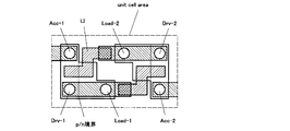
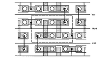
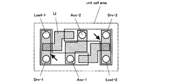
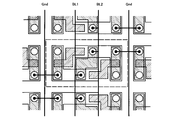
- FIG. 10 is a circuit diagram showing an example of the SRAM memory cell of the present embodiment.
- the first load transistor Load-1 that is a p-type transistor and the first driver transistor Drv-1 that is an n-type transistor constitute a first inverter.
- the second load transistor Load-2, which is a p-type transistor, and the second driver transistor Drv-2, which is an n-type transistor, constitute a second inverter.
- the output node N1 of the first inverter is input to the second inverter via the connection gate electrode of the second inverter
- the output node N2 of the second inverter is input to the second inverter via the connection gate electrode of the first inverter. 1 is input to the inverter.
- the nodes N1 and N2 constitute an accumulation node. If one node is at the ground potential (Gnd), the other is at the power supply potential (Vdd), and if one is at the power supply potential (Vdd), the other is at the ground potential (Gnd).
- the memory cell stores information with the above two states as the “1” state or the “0” state.
- the storage node N1 is connected to the first bit line BL1 via the first access transistor Acc-1 which is an n-type transistor.
- the storage node N2 is connected to the bit line BL2 via a second access transistor Acc-2 which is an n-type transistor.
- the gate electrodes of the two access transistors Acc-1 and Acc-2 are connected to a common word line Word.
- the upper conductive region opposite to the storage node of the two load transistors Load-1 and Load-2 is connected to the power supply line Vdd.
- the upper conductive region on the opposite side of the storage nodes of the two driver transistors Drv-1 and Drv-2 is connected to the ground line Gnd.
- each of the six vertical transistors constituting the memory cell has a pair of a lower conductive region and an upper conductive region.
- the lower conductive region is electrically connected to any one of the storage nodes N1 or N2.
- the storage node N1 or N2 only needs to be electrically connected to the gate electrode of the vertical transistor in the memory cell, and is electrically connected to any of the wirings (Vdd, Gnd, BL1, BL2, Word) connected to the outside of the cell. Not connected to.
- the same materials as those of the transistors constituting the first and second inverters can be used. .
- the semiconductor device constituting the SRAM of this embodiment has the following effects. (1) By using six transistors constituting a memory cell as vertical transistors, the area occupied by the transistors can be reduced. (2) Of each vertical transistor, the source or drain connected to the gate electrode can be disposed on the lower side as the lower conductive region. As a result, the area of the memory cell can be easily miniaturized. (3) The gate electrode is directly electrically connected to the other lower conductive region in the same memory cell without using a contact plug and an external wiring. For this reason, it is not necessary to provide a region for electrically connecting the lower conductive region to the contact plug and the external wiring, and the area of the memory cell can be reduced and miniaturization can be easily performed.
- the wiring resistance can be as low as that of a planar transistor. As a result, a high performance SRAM can be realized.
- Electrical connection to the external wiring is made through the upper conductive regions of the first and second access transistors Acc-1 and Acc-2. Therefore, it is possible to easily make contact with the external wiring without occupying an extra area.
- the semiconductor device can be manufactured by a simple manufacturing process.
- each vertical transistor can take various arrangements.
- the specific arrangement of the vertical transistors constituting the SRAM memory cell and the wiring structure for electrically connecting the inverters will be described by way of examples. However, the present invention is limited to the following examples. It is not done.
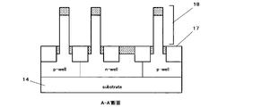
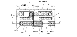
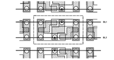
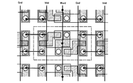
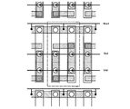
- FIG. 11A is a top view showing an example of a memory cell
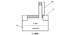
- FIG. 11B is a cross-sectional view taken along the line AA ′ of FIG. 11A
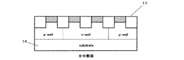
- FIG. 12A is a cross-sectional view taken along the line BB ′ of FIG. 'Cross section.
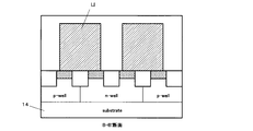
- FIG. 11A hatching of the portion constituting the lower conductive region is omitted.
- the gate insulating film is usually extremely thin, the gate insulating film is not shown in FIGS. Note that, in the drawings subsequent to FIG. 13, the gate insulating film and the lower conductive region are not hatched in the top view.
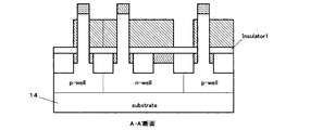
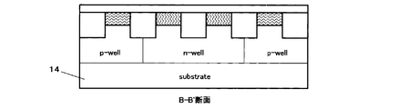
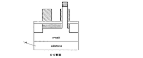
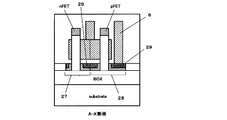
- the memory cell is formed using a bulk semiconductor substrate.
- Si is typically used, but SiGe, Ge, or other semiconductors may be used.
- This memory cell is composed of six vertical transistors, and each transistor has a column part 18 projecting upward from the base part surface 17 of the semiconductor substrate. Further, the upper part of each column part 18 is an upper conductive region. Further, a gate insulating film and a gate electrode are provided on the side surface of the column portion. When each transistor is turned on, a column portion between the lower conductive region and the upper conductive region becomes a channel region, and a channel current flows between the lower conductive region and the upper conductive region. In the lower conductive region of each transistor, a region in a direction parallel to the surface direction of the substrate is defined by an element isolation insulator (STI), and a lower boundary is defined by the depth of the element isolation insulator.
- STI element isolation insulator
- the lower conductive region and the upper conductive region are heavily doped n-type semiconductor regions, and the column portion between the lower conductive region and the upper conductive region is typically doped to a low concentration n or p-type. It has become a semiconductor region.
- the lower conductive region and the upper conductive region are typically high-concentration p-type semiconductor regions, and the semiconductor region between the lower conductive region and the upper conductive region is typically low-concentration n or p. It is a semiconductor region doped in the mold.
- the base portions of the first access transistor Acc-1 and the first driver transistor Drv-1 are integrally formed to form a first connection base portion.
- the lower conductive region of the first access transistor and the lower conductive region of the first driver transistor are electrically connected without using a wiring to form a part of the first storage node.
- the lower conductive region of the first load transistor Load-1 is formed separately from the base portions of the first access transistor and the first driver transistor.
- the lower conductive region of the second access transistor Acc-2 and the second driver transistor Drv-2 are integrally formed to form the second connection base portion. Yes.
- the lower conductive region of the second access transistor and the lower conductive region of the second driver transistor are electrically connected without using a wiring to form a part of the second storage node.
- the lower conductive region of the second load transistor Load-2 is formed separately from the base portions of the second access transistor and the second driver transistor.
- the reason why the lower conductive region of the n-type transistor and the lower conductive region of the p-type transistor that constitute the same inverter is separated is short-circuited between the power supply and the ground, resulting in malfunction. This is to prevent the occurrence of. That is, this is to prevent the lower conductive region (n-type) of the n-type transistor from being short-circuited with the power supply via the n-well. Another reason is to prevent the lower conductive region (p-type) of the p-type transistor from being short-circuited to the ground via the p-well.
- the second driver transistor and the second load transistor constitute a second connection gate electrode 5 formed integrally, and this connection gate electrode 5 is leftward in the drawing.
- the second gate extension 30 is extended. That is, when viewed from above, the second gate extension 30 extends from above the lower conductive region 4 of the n-type and p-type transistors constituting the second inverter to the outside. .
- the lower conductive region 3 of the first access transistor, the first driver transistor, and the first load transistor is electrically connected to the second gate extension 30 by the first local wiring 6. ing.
- the lower conductive region 3, the gate electrode 5, and the first local wiring 6 of the first access transistor, the first driver transistor, and the first load transistor constitute a first storage node. .
- the first driver transistor and the first load transistor constitute a first connection gate electrode 7 formed integrally, and this connection gate electrode 7 is extended in the right direction in the drawing.
- a first gate extension 31 is provided. That is, when viewed from above, the gate extension 31 extends from above the lower conductive region 3 of the n-type and p-type transistors constituting the first inverter to the outside.
- the lower conductive region 4 of the second access transistor, the second driver transistor, and the second load transistor are electrically connected to the first gate extension 31 by the third local wiring 9. ing.
- the lower conductive region 4, the gate electrode 7, and the third local wiring 9 of the second access transistor, the second driver transistor, and the second load transistor constitute a second storage node. .
- the first local wiring 6 has a protrusion 19 and a protrusion 20, and the lower surface of the protrusion 20 is in contact with the upper surface 15 of the connection gate electrode 5 and has the same height as the upper surface 15. It has become.
- the third local wiring 9 also has a convex portion and a protruding portion, like the first local wiring 6. The lower surface of the third local wiring 9 is in contact with the upper surface of the gate electrode 7 and has the same height as this surface.
- the upper conductive region of the first and second driver transistors is a ground line, and the upper conductive region of the first and second load transistors is a power line. Electrically connected.
- the upper conductive region of the first access transistor is electrically connected to the first bit line, and the upper conductive region of the second access transistor is electrically connected to the second bit line.
- the lower conductive region and the upper conductive region are not in contact with the gate insulating film, and the gate electrode is provided on the lower conductive region and the upper conductive region. It is not done.
- the lower conductive region and the upper conductive region of the vertical transistor of this embodiment are not limited to such a form.
- 13A and 13B are views showing a cross section of a portion corresponding to the A-A ′ cross section of FIG. 11A, and are views showing different shapes of the lower conductive region and the upper conductive region from FIG. 11B.
- the lower conductive region and the upper conductive region are present in a wider region up to the gate electrode side of the pillar portion and are in contact with the gate insulating film, and the gate electrode is formed on the lower conductive region and the upper conductive region. Is provided.
- each transistor and memory cell can be operated without any problem. Further, whether or not the lower conductive region and the upper conductive region are brought into contact with the gate insulating film in this manner is a region in which impurities for the lower conductive region and the upper conductive region are diffused in the pillar portion in the manufacturing process of the semiconductor device. And by controlling the region where the gate insulating film and the gate electrode are formed.
- a p-well and an n-well are formed as in the related planar type vertical transistor.
- the p-well exists in a region where an n-type transistor is provided, and is usually supplied with a ground potential (Gnd).
- the n-well exists in a region where a p-type transistor is provided, and is usually supplied with a power supply potential (Vdd). This ensures that the lower conductive region and the upper conductive region and the well and the n well and the p well are all reversely biased and insulated.
- the size and cross-sectional shape of the base portion of each transistor are the same. This increases the regularity of the pattern and facilitates processing. Further, the increase in the area of the base portion can increase the electric capacity of the storage node, and can stabilize the operation of the SRAM against disturbance. It should be noted that the load transistor base portion may be made smaller than the integrally formed access transistor and driver transistor base portion as long as it can be connected to the wiring. Each transistor is formed so as to have substantially the same height. In this embodiment, the transistors are not multilayered as disclosed in Patent Documents 1 and 6, and the manufacturing process can be simplified.
- FIG. 14 shows a plurality of memory cells of FIGS. 11 and 12 arranged in an array, and for each memory cell, a power supply line Vdd, a ground line Gnd, first and second bit lines BL1 and BL2, a word line It is a figure showing an example of the semiconductor device which electrically connected Word.
- a rectangular broken line area corresponds to a single memory cell. Assuming that the minimum width and the minimum interval of each structure in FIG. 14 are both F, the dimensions of this memory cell are approximately 8F in width and 4F in width, and 32F 2 when the area is ideal. It becomes.
- FIG. 14 shows an example in which memory cells are similarly arranged in the vertical direction as mirror images.
- the arrangement method of the memory cells is not limited to this, and the unit cells may be arranged in the vertical direction so as to be translated (cells are simply arranged in parallel). This is because, in any case, the connection portion of the wiring cannot be shared between adjacent memory cells.
- a desired region is protected by providing a mask by lithography technology, and the substrate is selectively etched only in the region of the semiconductor substrate that is not protected, thereby removing the substrate in the region that becomes the element isolation insulator.
- the surface of the insulator is flattened by a CMP technique. Further, an element isolation insulator is formed by selectively etching back the insulator.
- an n-type impurity is ion-implanted vertically from above, so that the upper portion of the column portion for the n-type transistor and the vicinity of the base are formed.
- the upper conductive region and the lower conductive region are formed, respectively.
- the region for forming the n-type transistor is covered with the mask.
- an upper conductive region and a lower conductive region are formed in the upper portion of the column portion for the p-type transistor and in the vicinity of the root thereof, respectively.
- the mask covering the region for forming the n-type transistor is removed. Note that the order of forming the lower and upper conductive regions of the n-type transistor and the lower and upper conductive regions of the p-type transistor may be reversed. In order to form the lower conductive region as shown in FIGS. 13A and 13B, the source and drain impurities may be appropriately diffused in the gate direction in the manufacturing process.
- FIGS. 15 and 16 were obtained.
- 15A is a top view showing an intermediate manufacturing process
- FIG. 15B is a cross-sectional view taken along line AA ′ of FIG. 15A
- FIG. 16A is a cross-sectional view taken along line BB ′ of FIG. 15A
- FIG. A sectional view is shown.
- the upper conductive region and the lower conductive region can be simultaneously formed in the upper portion of the pillar portion and in the vicinity of the root thereof.
- the surface of the insulator is flattened by a CMP technique. Thereafter, the insulator is selectively etched back to form a first insulator film having the same height as the lower end of the gate electrode to be formed later and covering the entire surface of the region where the pillar portion does not exist. . Next, the surface of the column portion is covered with a gate insulating film by thermal oxidation or CVD. Next, after depositing a metal which is a gate electrode material so as to have a thickness higher than that of the pillar portion, the surface of the metal is flattened by a CMP technique.
- FIGS. 17 and 18 were obtained.
- 17A is a top view showing an intermediate manufacturing process
- FIG. 17B is a cross-sectional view taken along line AA ′ of FIG. 17A
- FIG. 18A is a cross-sectional view taken along line BB ′ of FIG. 17A
- FIG. A sectional view is shown.
- an insulator film covering the entire surface is formed by flattening the surface of the insulator by a CMP technique.
- a desired region was protected with a mask formed by a lithography technique, and the insulating film was selectively etched only in the unprotected region to form a trench for embedding the wiring.
- the surface of the conductor is flattened by a CMP technique, so that the conductor is embedded in the groove to form a wiring.
- the structure shown in FIGS. 11 and 12 can be obtained by forming an insulator on the entire surface.
- a high melting point metal such as tungsten which has been conventionally used for contact embedding can be used.
- tungsten it is preferable to stack tungsten on a thin barrier film such as titanium nitride.
- FIG. 19 and 20 are diagrams showing another example of the memory cell.
- 19A is a top view showing the memory cell of this embodiment
- FIG. 19B is a cross-sectional view taken along line AA ′ of FIG. 19A
- FIG. 20A is a cross-sectional view taken along line BB ′ of FIG. 19A
- FIG. A sectional view is shown.
- This embodiment is different from the seventh embodiment in that a semiconductor thin film is provided on an insulator and a lower conductive region of each transistor is formed in the semiconductor thin film.
- a typical example of a substrate having a semiconductor thin film on an insulator is a silicon-on-insulator (SOI) substrate.
- SOI silicon-on-insulator
- the semiconductor thin film may be made of SiGe, Ge, or another semiconductor. good.
- the lower conductive region of the first load transistor is integrally formed in addition to the first access transistor and the first driver transistor, and a part of the first storage node is formed.
- a base member belonging to the above is configured. That is, the base portion of the first access transistor, the base portion of the first driver transistor, and the base portion of the first load transistor are integrated to form a first connection base portion.
- the lower conductive region of the second load transistor is integrally formed, and the base portion belonging to a part of the second storage node is formed. This is different from the seventh embodiment. That is, the base portion of the second access transistor, the base portion of the second driver transistor, and the base portion of the second load transistor are integrated to form a second connection base portion.
- the lower conductive region (n-type) of the n-type transistor is short-circuited to the power supply via the n-well because the lower portion of the semiconductor thin film is insulated by the buried insulator. There is nothing. Further, the lower conductive region (p-type) of the p-type transistor is not short-circuited to the ground via the p-well.
- the lower conductive region of the n-type transistor and the lower conductive region of the p-type transistor are usually not necessarily short-circuited only by direct contact. Therefore, the local wiring is formed so as to straddle the lower conductive region (n-type region) of the n-type transistor constituting the same inverter and the lower conductive region (p-type region) of the p-type vertical transistor. Can do.
- the lower conductive region and the upper conductive region are semiconductor regions doped with impurities.
- the lower conductive region 3 of the first access transistor, first driver transistor, and first load transistor is electrically connected to the connection gate electrode 5 by the first local wiring 6.
- the lower conductive region 4 of the second access transistor, the second driver transistor, and the second load transistor are electrically connected to the connection gate electrode 7 by the second local wiring 9. ing.
- connection portion between the first local wiring 6 and the connection gate electrode 5 is the second gate extension portion of the first local wiring and the connection gate electrode 5 (the gate electrode is located above the second connection base portion). (Part extending to a region other than) is represented by a portion 10 where 30 overlaps. The connection portion 10 is a region other than the upper side of the second connection base portion SD2. Further, in FIG. 19A, the connection portion between the second local wiring 9 and the connection gate electrode 7 is the first gate extension portion of the second local wiring and the connection gate electrode 7 (the gate electrode is located above the first connection base portion). (Part extending to a region other than) is represented by a portion 10 where 31 overlaps. The connection portion 10 is a region other than the upper portion of the first connection base portion SD1.
- the first local wiring 6 has a convex portion 19 and a projecting portion 20, and the lower surface of the projecting portion 20 is in contact with the upper surface 15 of the connection gate electrode 5 and is the same height as the upper surface 15. It has become.
- the third local wiring 9 also has a convex portion and a protruding portion, like the first local wiring 6. Further, the lower surface of the third local wiring 9 is in contact with the upper surface of the connection gate electrode 7 and has the same height as this surface.
- the connection portion between the first and third local wirings 6 and 9 and the connection gate electrode has the above-described structure, the first and third local wirings are formed in one lithography process. be able to. Furthermore, since the height of the first and third local wirings can be reduced, the height of the upper wiring is increased by using the local wiring (the upper wiring needs to be separated from the local wiring by a certain distance). Can be suppressed.
- connection method between the lower conductive regions is not limited to the above method.
- a silicide layer may be formed on a semiconductor region doped with impurities by a salicide technique, and the lower conductive regions may be electrically connected by this silicide layer.
- the lower conductive region of the n-type and p-type transistors may be electrically connected by being made of a metal material.
- the lower conductive region of the n-type and p-type transistors is made of a metal material or has a salicide structure, so that the lower conductive regions of the n-type and p-type transistors are directly brought into contact with each other. It will be automatically connected electrically. Therefore, in such a case, it is not necessary to form a local wiring that is electrically connected across the lower conductive region of the n-type and p-type transistors, and the process can be simplified.
- a metal such as Ni silicide is formed in a self-aligned manner only on the surface of the lower conductive region. Further, the insulating protective film is removed as necessary.
- the lower conductive region may be completely made of metal so that the lower conductive region formed by ion implantation is completely silicided.
- the n-type and p-type impurities implanted in advance are adjusted so that the effective work functions of the metal source and the drain are preferably adjusted for the n-type vertical transistor and the p-type vertical transistor. Can be made.
- FIG. 38 shows an example of a semiconductor device having a salicide structure.
- 38A to 38C are views corresponding to cross sections in the A-A ′ direction, the B-B ′ direction, and the C-C ′ direction, respectively, of the semiconductor device of FIG. 19A.
- the first connection base portion SD1 includes a first conductivity type semiconductor region 27 and a second conductivity type semiconductor region 28 joined to the first conductivity type semiconductor region 27.
- the first and second conductive semiconductor regions 27 and 28 form a two-dimensional planar region when viewed from above (in the normal direction of the substrate surface).
- the first conductive type semiconductor region 27 is provided with a column portion of the first n-type transistor.
- the second conductive semiconductor region 28 is provided with a column portion of the first p-type transistor.
- the second connection base portion SD2 in the same manner as the first connection base portion SD1, includes a first conductive type semiconductor region 27, a second conductive type semiconductor region 28, and a silicide layer 29.
- the first and second conductivity type semiconductor regions are electrically connected.
- the area can be further reduced by using the first and second connection base portions in which the n-type and p-type lower conductive regions are connected and integrated.
- connection means of the lower conductive region 3 of the n-type and p-type transistors is not limited to the silicide layer.
- each lower conductive region 3 is made of a metal material, whereby the adjacent lower conductive regions 3 can be electrically connected.
- the shape of the local wiring is not limited to that of the present embodiment, and can be appropriately selected.
- the shape of the local wiring is Has a high degree of freedom.
- the metal region or the salicide structure wiring can be formed so that the upper part or the whole of the lower conductive region of the n-type and p-type transistors is electrically connected continuously. This eliminates the need for the local wiring to straddle the lower conductive region of the n-type and p-type transistors. For this reason, even when the miniaturization is advanced, the first and second local wirings can be easily formed.
- FIG. 21 and 22 are views showing a structure in the middle of manufacture of this example.
- 21A is a top view showing an intermediate manufacturing process
- FIG. 21B is a sectional view taken along line AA ′ in FIG. 21A
- FIG. 22A is a sectional view taken along line BB ′ in FIG. 21A
- FIG. A sectional view is shown.
- the first access transistor, the first driver transistor and the first load transistor, and the second access transistor, the second driver transistor and the first The planar structure of the base portion of the second load transistor is substantially square. This simplifies the pattern and facilitates its processing. Further, the increase in the area of the base portion increases the electric capacity of the storage node, and the operation of the SRAM can be stabilized against disturbance.
- the shape of the base portion is not limited to a substantially square shape, and the shape of the base portion can be a desired shape.
- the cell area can be reduced by appropriately changing the shape of the base portion.
- FIG. 23 shows another example of a semiconductor device having a different arrangement of transistors.
- the base portions of the first access transistor, the first driver transistor, and the first load transistor are integrated to form a first connection base portion.
- the base parts of the second access transistor, the second driver transistor, and the second load transistor are integrated to form a second connection base part.
- the semiconductor device of FIGS. 19 and 20 is different in that the planar structure of these integrated connecting base portions is not substantially square.
- the shape of the square apex of the base portion is set so that the vicinity of the apex where none of the transistors are arranged close to each other is retreated.
- the first access transistor is opposed to the second load transistor, and the second access transistor is opposed to the first load transistor. This shortens the distance between the first access transistor and the second load transistor and the distance between the second access transistor and the first load transistor.
- the horizontal width of the unit cell can be reduced from about 8F to 7F, and the cell area can be reduced from 32F 2 to 28F 2 .
- substrate part which can reduce such a cell area can be suitably selected from various choices.
- FIG. 24 is a diagram illustrating another example of the memory cell.
- 24A is a top view of the semiconductor device
- FIG. 24B is a cross-sectional view taken along line AA ′ of FIG. 24A.
- a semiconductor thin film is provided on an insulator, and a lower conductive region of each transistor is formed in the semiconductor thin film.
- the semiconductor device of this example is different from the eighth example in the arrangement of the transistors and the position to which the wiring on the gate electrode is connected. Also in this embodiment, restrictions on the wiring structure are reduced, and the cell area can be easily reduced.
- the portion where the first and third local wirings are connected to the connecting gate electrode is an extended portion extending to a region other than the upper portion of the connecting base portion constituting each inverter.
- the first local wiring 6 is connected between the column portion of the second n-type transistor and the column portion of the second p-type transistor. Connected to the electrode 5.
- the first local wiring 6 is connected to the connection gate electrode 5 above the second connection base portion SD2, and the first local wiring 6 is insulated from the second connection base portion SD2. .
- the third local wiring 9 is connected to the connection gate electrode 7 between the column portion of the first n-type transistor and the column portion of the first p-type transistor. Further, the third local wiring 9 is connected to the connection gate electrode 7 above the first connection base portion SD1, and the third local wiring 9 is insulated from the first connection base portion SD1 while being separated from the first connection base portion SD1. .
- the first local wiring 6 has a convex portion 19 and a protruding portion 20, and the protruding portion 20 has two lower surfaces. Among these, one lower surface of the projecting portion comes into contact with the upper surface 15 of the connecting gate electrode 5 and becomes the same height as the upper surface 15, and the other lower surface 22 of the projecting portion is present on the substrate surface 17 side of the upper surface 15. ing.
- the third local wiring 9 also has a convex portion and a protruding portion, like the first local wiring 6.
- the protruding portion of the third local wiring 9 has a lower surface that is in contact with the upper surface of the connection gate electrode 6 and has the same height as the upper surface, and a lower surface that is located closer to the base body surface 17 than the upper surface.
- a connection portion between the first local wiring 9 and the connection gate electrode 5 is represented by a portion 10 where the first local wiring and the gate electrode overlap in FIG. 24A.
- the height of the first and third local wirings can be reduced, the height of the upper wiring is increased by using the local wiring (the upper wiring needs to be separated from the local wiring by a certain distance). Can be suppressed.
- the above effects are the same in the inverters shown in the third, fourth and sixth embodiments.
- the first and third local wirings may be formed in two stages. That is, an example in which one local wiring is formed will be described below as an example.
- a wide groove that reaches the gate electrode but does not reach the lower conductive region is provided in the insulating film by the first lithography and etching process.
- FIG. 25B a narrow groove reaching only the lower conductive region to be electrically connected is formed by the second lithography and etching process.
- local wiring is formed by embedding a conductor in the wide and narrow grooves shown in FIGS. 25A and 25B.
- the contact hole and the local wiring are formed by two lithography processes in the same manner as the related wiring structure in which the contact holes and the local wiring are formed by separate lithography processes.
- the pattern formation corresponding to the contact hole for the gate electrode is omitted.
- the local wiring can be miniaturized as compared with arranging one contact hole at each of the two points to be connected.
- the lower surface of the protruding portion of the local wiring is disposed at a height equal to or lower than the upper surface of the gate electrode.
- the local wiring has a structure in contact with at least a part of the side surface of the gate electrode in order to reduce contact resistance. In order to obtain this advantage, the local wiring is not applied to the wiring that intersects the gate electrode without contacting the gate electrode.
- the local wiring in FIG. 24B and the local wiring in FIG. 12B can be mixed on the same substrate without complicating the manufacturing process. Since only the formation of the deep groove for obtaining the structure of FIG. 24B is applied and the formation of the shallow groove is omitted, the structure of FIG. 12B can be obtained. Therefore, a special process is added to the process of forming the structure of FIG. 24B. The structure of FIG. 12B can be formed without this.
- the lower conductive regions of the load transistor and the driver transistor are connected by the base portion, and the gate electrodes of the load transistor and the driver transistor are also connected thereabove.
- the gate electrode and the base portion are arranged at substantially the same position when viewed from above the substrate, but they are separated from each other in the vertical direction and function as independent wiring.
- Such a structure is peculiar to the vertical transistor. This is because, in an ordinary planar transistor, when viewed from above the substrate, if the semiconductor region corresponding to the base portion and the gate electrode are arranged so as to overlap at the same position, the element region in this overlapping region has a channel portion. This is because is automatically formed. As a result, the channel portion in the overlapping region cannot function as a wiring.
- the high density of the SRAM cell is realized by combining the structure peculiar to this vertical transistor with the local wiring structure of FIG. 24B.
- FIG. 26 is a diagram showing a semiconductor device in which a plurality of memory cells of FIG. 24 are arranged in an array and the power supply line Vdd, the ground line Gnd, the first and second bit lines BL1 and BL2, and the word line Word are connected. It is. 26A shows the bit line and the ground line Gnd, and FIG. 26B shows the word line and the power supply line Vdd, respectively.
- a rectangular broken line area is a memory cell. Note that the arrangement of the memory cells in the horizontal direction is arranged in a mirror image symmetry with the boundary line of the memory cells as the center, as in FIG. Thereby, the connection portion between the word line and the gate electrode of the access transistor can be shared between adjacent cells, and the degree of integration can be increased.
- FIG. 26 shows an example in which cells are similarly arranged in the vertical direction in the mirror image object, but unit cells may be arranged in the vertical direction as objects to be translated.
- FIG. 28 and 29 are semiconductor devices in which a plurality of the memory cells of FIG. 27 are arranged in an array, and the power supply line Vdd, the ground line Gnd, the first and second bit lines BL1 and BL2, and the word line Word are connected.
- FIG. 28A shows a word line and a power supply line Vdd
- FIG. 28B shows a bit line and a ground line Gnd.
- FIG. 29A shows a bit line
- FIG. 29B shows a word line and wiring (Vdd, Gnd). 28 the word lines are formed in the horizontal direction and the bit lines are formed in the vertical direction.
- the bit lines are formed in the horizontal direction and the word lines are formed in the vertical direction.
- this embodiment has an advantage that the direction in which the word line and the bit line run can be selected as appropriate. In other embodiments, it is not impossible to change the direction in which the word line and the bit line run, but if the direction in which the word line and the bit line run is changed due to layout restrictions, unnatural wiring is required. It may become.
- FIG. 32 shows a semiconductor device in which a plurality of cells shown in FIG. 31 are arranged in an array, and the power supply line Vdd, the ground line Gnd, the first and second bit lines BL1 and BL2, and the word line Word are electrically connected. It is a figure showing an example. 32A shows word lines and wirings (Vdd, Gnd), and FIG. 32B shows bit lines.
- the arrangement of cells in the horizontal direction is mirror-symmetric with respect to the boundary of the unit cells, and the arrangement of cells in the vertical direction is translational symmetry. Even if it is arrangement
- FIG. 33 is a diagram illustrating another example of the memory cell.
- the present embodiment relates to a memory cell having a lower conductive region in a semiconductor thin film formed on an insulator.
- the gate electrode of one inverter and the base portion of the lower conductive region of the other inverter protrude so as to face each other in a lateral direction, and are easily electrically connected to each other.
- the cell of this embodiment has a horizontal width of about 5F and a vertical width of about 6F, and a memory cell with an area of 30F 2 can be realized.
- the method of connecting the power supply line Vdd, the ground line Gnd, the first and second bit lines BL1 and BL2, and the word line Word is the same as in the eleventh embodiment. As good.
- the tenth to twelfth embodiments have a feature that the gate electrode of the access transistor can be continuously formed across adjacent cells.
- the gate electrode itself of the access transistor can also be used as the word line wiring, and it is possible to omit separately providing the word line wiring above.
- the number of contacts can be reduced by providing the contact between the word line wiring and the gate electrode of the access transistor not for each cell but for each of a plurality of cells without omitting the upper word line wiring. .
- FIG. 34 shows a schematic diagram for organizing and capturing the memory cells of the above-described Examples 7 to 12.
- circles indicate the positions of the vertical transistors.
- a rectangle including the two circles indicates an inverter composed of a driver transistor and a load transistor.
- a square including one circle indicates an access transistor.
- a solid line (connecting line) connecting the squares symbolically indicates that the connected squares belong to the same storage node (first or second storage node).
- the positional relationship between the n-type transistor and the p-type transistor is limited. This is because the base portion of the n-type transistor and the p-type transistor is insulated by the well, but the well needs to have a continuous pattern when the memory cells are arranged so that a constant potential can be applied from the outside. Because. For example, in FIG. 14, in the seventh embodiment, the n-well and the p-well occupy a continuous band-like region so that a well potential can be applied to the outer periphery of the aligned cells. In order to realize a similar arrangement when the access transistor is a p-type transistor, the positions of the driver transistor and the load transistor may be switched.
- the degree of freedom in the positional relationship between the n-type transistor and the p-type transistor is increased. That is, the positions of the driver transistor and the load transistor can be switched as appropriate.
- the first and second access transistors are p-type transistors, it is not always necessary to interchange the positions of the driver transistor and the load transistor.
- it is difficult to form the local wiring so as to straddle the lower conductive region of the n-type transistor and the lower conductive region of the p-type transistor. In such a case, it is desirable that these lower conductive regions are made of metal or have a salicide structure.
- the lower conductive region of the n-type and p-type transistors adjacent to each other can be used by using a salicide structure.
- the lower conductive region can be automatically electrically connected, for example, by being made of a metal material.
- the positions of the first driver transistor and the first load transistor are switched appropriately, or the second driver transistor and the second load transistor are appropriately switched within a range that does not interfere with the arrangement of the upper layer wiring. It is possible to change the position. However, in this case, it is necessary to change the wiring of Vdd and Gnd in the upper layer.
- FIG. 24A the positions of the first driver transistor and the first load transistor are interchanged, and the positions of the second driver transistor and the second load transistor are interchanged.
- Vdd and Gnd Can be replaced.
- the driver transistor is an n-type transistor and the load transistor is a p-type transistor.
- the types of the driver transistor and the load transistor are not limited to this, and the driver transistor may be a p-type transistor and the load transistor may be an n-type transistor.
- exchanging the n-type and the p-type in this way is completely equivalent to exchanging the positions of the driver transistor and the load transistor in the above description. Therefore, even if the driver transistor is limited to n-type and the load transistor is limited to p-type, the generality of the description is not lost.
- the first n-type transistor is the first transistor and the first p-type transistor is the third transistor.
- the first and third transistors are not limited to n-type and p-type transistors, respectively.
- the first n-type transistor is the third transistor, and the first p-type transistor is the first transistor. It is good also as this transistor.
- the second and fourth transistors are not limited to n-type and p-type transistors, respectively.
- the second n-type transistor is the fourth transistor, and the second p-type transistor is the second transistor.
- a second transistor may be used.
- wiring running in the horizontal direction and the wiring running in the vertical direction need to be formed in different steps in different layers so as not to short-circuit each other.
- wirings running in the horizontal direction or wirings running in the vertical direction may be appropriately formed in separate steps.
- the ground line Gnd and the word line Word may be formed in separate steps.
- the wirings formed in separate steps can be arranged closer to each other than the minimum pitch limited by the resolution of the lithography technique, and the wiring density can be increased.
- the sectional structure of the vertical transistor viewed from above is circular, but the sectional structure is not limited to a circular shape, and may be changed as appropriate, such as an ellipse or a rectangle.
- each part is determined with the following restrictions. That is, the dimension of each element such as the base portion, the gate electrode, the wiring, and the transistor viewed from above is at least approximately F or more. In addition, the distance between the base portions, the gate electrodes, the wirings, and the transistors viewed from above is at least approximately F or more. In order to establish electrical connection between elements, an overlap of approximately F or more is provided. With a cell structure that satisfies these restrictions, it is possible to manufacture a cell using a manufacturing apparatus that actually has the capability of the minimum line width F.
- the semiconductor device of the present invention can be mounted on various integrated circuits, and in particular, can be used as an SRAM.
Landscapes
- Engineering & Computer Science (AREA)
- Power Engineering (AREA)
- Microelectronics & Electronic Packaging (AREA)
- Condensed Matter Physics & Semiconductors (AREA)
- General Physics & Mathematics (AREA)
- Physics & Mathematics (AREA)
- Computer Hardware Design (AREA)
- Ceramic Engineering (AREA)
- Manufacturing & Machinery (AREA)
- Metal-Oxide And Bipolar Metal-Oxide Semiconductor Integrated Circuits (AREA)
- Semiconductor Memories (AREA)
- Internal Circuitry In Semiconductor Integrated Circuit Devices (AREA)
- Thin Film Transistor (AREA)
- Insulated Gate Type Field-Effect Transistor (AREA)
Abstract
Description
少なくとも第1および第2のトランジスタ、並びに第1局所配線を備えた半導体装置であって、
第1および第2のトランジスタは、
基体部表面から突出した半導体からなる柱部と、
前記基体部に設けられたソースおよびドレインの一方となる下側導電領域と、
前記柱部の上部に設けられたソースおよびドレインの他方となる上側導電領域と、
前記柱部の側面上に設けられたゲート電極と、
前記ゲート電極と前記柱部との間に介在するゲート絶縁膜と、
を備え、
第1局所配線は、
基体部表面から突出した凸部と、
前記凸部の側面から突出した突出部と、
を備え、
第1局所配線の凸部は、第1のトランジスタの下側導電領域に接続され、
第1局所配線の突出部は、第2のトランジスタのゲート電極に接続され、
第1局所配線の突出部の下面は、第2のトランジスタのゲート電極の上面以下の高さに配置される、
ことを特徴とする半導体装置に関する。 One embodiment of the present invention
A semiconductor device comprising at least first and second transistors and a first local wiring,
The first and second transistors are:
A pillar portion made of a semiconductor protruding from the surface of the base portion;
A lower conductive region serving as one of a source and a drain provided in the base portion;
An upper conductive region serving as the other of the source and the drain provided on the upper part of the column part;
A gate electrode provided on a side surface of the column part;
A gate insulating film interposed between the gate electrode and the pillar portion;
With
The first local wiring is
Convex portions protruding from the surface of the base portion;
A protrusion protruding from the side surface of the protrusion;
With
The convex portion of the first local wiring is connected to the lower conductive region of the first transistor,
The protruding portion of the first local wiring is connected to the gate electrode of the second transistor,
The lower surface of the protruding portion of the first local wiring is disposed at a height equal to or lower than the upper surface of the gate electrode of the second transistor.
The present invention relates to a semiconductor device.
少なくとも第1および第2のトランジスタ、並びに第1局所配線を備えた半導体装置の製造方法であって、
(1)基体部表面から突出した半導体からなる柱部と、
前記基体部に設けられたソースおよびドレインの一方となる下側導電領域と、
前記柱部の上部に設けられたソースおよびドレインの他方となる上側導電領域と、
前記柱部の側面上に設けられたゲート電極と、
前記ゲート電極と前記柱部との間に介在するゲート絶縁膜と、
を備えた第1および第2のトランジスタを形成する工程と、
(2)前記基体部表面から突出した凸部と、
前記凸部の側面から突出した突出部と、
を備え、
前記凸部は、第1のトランジスタの下側導電領域に接続され、
前記突出部は、第2のトランジスタのゲート電極に接続され、
前記突出部の下面は、第2のトランジスタのゲート電極の上面以下の高さに配置される、第1局所配線を形成する工程と、
を有することを特徴とする半導体装置の製造方法に関する。 In addition, other embodiments of the present invention
A method of manufacturing a semiconductor device including at least first and second transistors and a first local wiring,
(1) a pillar portion made of a semiconductor protruding from the surface of the base portion;
A lower conductive region serving as one of a source and a drain provided in the base portion;
An upper conductive region serving as the other of the source and the drain provided on the upper part of the column part;
A gate electrode provided on a side surface of the column part;
A gate insulating film interposed between the gate electrode and the pillar portion;
Forming first and second transistors comprising:
(2) a convex portion protruding from the surface of the base portion;
A protrusion protruding from the side surface of the protrusion;
With
The convex portion is connected to the lower conductive region of the first transistor,
The protrusion is connected to the gate electrode of the second transistor;
Forming a first local wiring in which the lower surface of the protruding portion is disposed at a height below the upper surface of the gate electrode of the second transistor;
The present invention relates to a method for manufacturing a semiconductor device.
Drv-1、Drv-2: ドライバ・トランジスタ
Load-1、Load-2: ロード・トランジスタ
nSD: N型ソースおよびドレイン
pSD: P型ソースおよびドレイン
STI: 素子分離絶縁体
LI: 配線
IC: 配線
BOX: 埋め込み絶縁体
SD1 第1の連結基体部
SD2 第2の連結基体部
Gate ゲート電極
1 第1インバータ
2 第2インバータ
3、4、14 下側導電領域、連結基体部
5 第2の連結ゲート電極
7 第1の連結ゲート電極
6 第1局所配線
8 コンタクトプラグ
9、13 配線
11a、11b 第3インバータ
12 第1のトランジスタ
13 第2のトランジスタ
14 基板
15 ゲート電極の上面
17 基体部表面
18 柱部
19 凸部
20 突出部
21 上側導電領域
22 局所配線の下面
23 局所配線の上面
27 第1導電型半導体領域
28 第2導電型半導体領域
29 シリサイド層 Acc-1, Acc-2: Access transistor Drv-1, Drv-2: Driver transistor Load-1, Load-2: Load transistor nSD: N-type source and drain pSD: P-type source and drain STI: Device Isolation insulator LI: Wiring IC: Wiring BOX: Embedded insulator SD1 First connection base portion SD2 Second connection base portion
図36Aは、第1局所配線の凸部19の側面がゲート電極5の側面と接触しておらず、第1局所配線の下面22のみがゲート電極5の上面15に接触する半導体装置を表している。この半導体装置では、下面22はゲート電極5の上面15と同じ高さとなっている。 In the following, another mode in which the first local wiring and the gate electrode of the second transistor are electrically connected is shown in FIGS. In the following drawings, description of each part is omitted.
FIG. 36A shows a semiconductor device in which the side surface of the
次に、本発明の実施形態について図面を参照して詳細に説明する。 In the above description, the convex portion, the protruding portion, the lower surface, and the like of the first local wiring have been described. However, in the semiconductor device having the second and third local wirings, the second and third local wirings are also referred to as the first local wiring. Similarly, it has a convex part, a protrusion part, and a lower surface. Further, the lower surfaces of the protrusions of the second and third local wirings are arranged at a height that is lower than the upper surface of the gate electrode to which the protrusions are connected. Furthermore, the second and third local wirings can have the same effect as the first local wiring.
Next, embodiments of the present invention will be described in detail with reference to the drawings.
本発明の一実施形態は、インバータ・チェーンに関するものである。このインバータ・チェーンは、図2に示すインバータを、図3のように複数、連ねたものであり、バッファや遅延素子として用いることができる。このインバータ・チェーンにおいては、各インバータは、p型の縦型トランジスタとn型の縦型トランジスタとから構成されている。このように縦型トランジスタからインバータを構成することによって、プレナー型トランジスタを使用した場合と比べて、トランジスタの占有面積を小さくすることができる。この結果、微細化を行なうことができる。 1. Inverter Chain An embodiment of the present invention relates to an inverter chain. This inverter chain is formed by connecting a plurality of inverters shown in FIG. 2 as shown in FIG. 3, and can be used as a buffer or a delay element. In this inverter chain, each inverter is composed of a p-type vertical transistor and an n-type vertical transistor. By constructing the inverter from the vertical transistors in this way, the area occupied by the transistors can be reduced as compared with the case where planar transistors are used. As a result, miniaturization can be performed.
図4Aは、本実施例における、第1インバータ1と第2インバータ2とから構成される、2段インバータ・チェーンを表す上面図である。第1インバータ1は、第1のn型のトランジスタ(nFET)(第1のトランジスタに相当する)、第1のp型のトランジスタ(pFET)(第3のトランジスタに相当する)から構成されている。また、第2インバータ2は、第2のn型のトランジスタ(nFET)(第2のトランジスタに相当する)、第2のp型のトランジスタ(pFET)(第4のトランジスタに相当する)から構成されている。 (First embodiment)
FIG. 4A is a top view showing a two-stage inverter chain including the
(第2実施例)
図5は、第1インバータ1、第2インバータ2、および2つの第3インバータ11a、11bとから構成される、4段インバータ・チェーンを表す上面図である。第3インバータ11a、11bは、それぞれ第3のn型のトランジスタ(nFET)(第5のトランジスタに相当する)、第3のp型のトランジスタ(pFET)(第6のトランジスタに相当する)から構成されている。この第5および第6のトランジスタの柱部、上側導電領域、下側導電領域、ゲート電極およびゲート絶縁膜は、第1~第4のトランジスタと同様の構造となっている。この第3のn型のトランジスタおよび第3のp型のトランジスタのゲート電極は連結されており、第3の連結ゲート電極を構成する。 In this embodiment, the local wiring includes the function of connecting the output of the inverter to the input of the next-stage inverter, and the lower conductive region of the n-type transistor and the lower conductive region of the p-type transistor that are separated from each other. Plays an electrical connection function. That is, two functions are realized simultaneously while preventing an increase in area.
(Second embodiment)
FIG. 5 is a top view showing a four-stage inverter chain including the
図6Aは、第1実施例とはトランジスタの配置が異なる2段インバータ・チェーンを示す上面図である。本実施例では、第1インバータ1を構成する第1のn型のトランジスタ(nFET)の下側導電領域と、第1のp型のトランジスタ(pFET)の下側導電領域とが連結して一体的に形成され、第1の連結基体部3を構成している。そして、これらの下側導電領域は、下側導電領域上に、サリサイド技術により設けられたシリサイド層により電気的に接続されている。同様にして、第2インバータ2を構成する第2のn型のトランジスタ(nFET)の下側導電領域と、第2のp型のトランジスタ(pFET)の下側導電領域とが連結して一体的に形成され、第2の連結基体部4を構成している。これらの下側導電領域は、下側導電領域上に、サリサイド技術により設けられたシリサイド層により電気的に接続されている。 (Third embodiment)
FIG. 6A is a top view showing a two-stage inverter chain having a different transistor arrangement from that of the first embodiment. In the present embodiment, the lower conductive region of the first n-type transistor (nFET) constituting the
図7は、第1インバータ1、第2インバータ2、および2つの第3インバータ1a、11bとから構成される、4段インバータ・チェーンを表す上面図である。本実施例では、第3インバータ11a、11bを構成する第3のn型のトランジスタ(nFET)の下側導電領域3と、第3のp型のトランジスタ(pFET)の下側導電領域3とが連結して一体的に形成され、第3の連結基体部を構成している。 (Fourth embodiment)
FIG. 7 is a top view showing a four-stage inverter chain including the
図8は、第3実施例とはトランジスタの配置が異なる2段インバータ・チェーンを示す上面図である。本実施例では、第1インバータ1を構成する第1のn型のトランジスタ(nFET)の下側導電領域と、第1のp型のトランジスタ(pFET)の下側導電領域とが連結して一体的に形成され、第1の連結基体部3を構成している。そして、これらの下側導電領域は、図41に示したように下側導電領域上にサリサイド技術により設けられたシリサイド層により電気的に接続されているか、または、下側導電領域を金属材料から構成することにより電気的に接続されている。 (5th Example)
FIG. 8 is a top view showing a two-stage inverter chain having a different transistor arrangement from the third embodiment. In the present embodiment, the lower conductive region of the first n-type transistor (nFET) constituting the
図9は、第3実施例とはトランジスタの配置が異なる2段インバータ・チェーンを示す上面図である。本実施例では、第1インバータ1を構成する第1のn型のトランジスタ(nFET)の下側導電領域と、第1のp型のトランジスタ(pFET)の下側導電領域とが連結して一体的に形成され、第1の連結基体部3を構成している。そして、これらの下側導電領域は、第5実施例と同様に電気的に接続されている。また、第1の連結基体部3は、第1局所配線6によって、第2の連結ゲート電極5と電気的に接続されている。なお、第1局所配線6と連結ゲート電極5の接続部分は、図9中では、第1局所配線と連結ゲート電極が重なった部分10で表される。また、第1局所配線6は、第2の連結基体部4とは離間して電気的に絶縁されている。このような局所配線の利用による効果は後に説明する第9実施例と同様である。 (Sixth embodiment)
FIG. 9 is a top view showing a two-stage inverter chain having a different transistor arrangement from that of the third embodiment. In the present embodiment, the lower conductive region of the first n-type transistor (nFET) constituting the
本発明の他の一実施形態は、SRAM(スタティックランダムアクセスメモリセル)に関するものである。このSRAMは、メモリセルを有し、このメモリセルは、第1のn型トランジスタと、第1のp型トランジスタと、第2のn型トランジスタと、第2のp型トランジスタと、第1および第2のアクセストランジスタと、第1及び第3局所配線と、を備える。第1インバータは、第1のn型トランジスタ(第1のトランジスタに相当する)および第1のp型トランジスタ(第3のトランジスタに相当する)から構成されている。第2インバータは、第2のn型トランジスタ(第2のトランジスタに相当する)および第2のp型トランジスタ(第4のトランジスタに相当する)から構成されている。 2. SRAM (Static Random Access Memory)
Another embodiment of the invention relates to an SRAM (Static Random Access Memory Cell). The SRAM includes a memory cell, and the memory cell includes a first n-type transistor, a first p-type transistor, a second n-type transistor, a second p-type transistor, A second access transistor; and first and third local wirings. The first inverter includes a first n-type transistor (corresponding to a first transistor) and a first p-type transistor (corresponding to a third transistor). The second inverter is composed of a second n-type transistor (corresponding to the second transistor) and a second p-type transistor (corresponding to the fourth transistor).
(1)メモリセルを構成する6つのトランジスタを縦型トランジスタとすることによって、トランジスタの占有面積を小さくすることができる。
(2)各縦型トランジスタのうち、ゲート電極と接続されるソースまたはドレインを、下側導電領域として全て下側に配置できる。この結果、メモリセルの面積を容易に微細化することができる。
(3)ゲート電極は、コンタクトプラグおよび外部配線等を介さずに、直接、同一のメモリセル内の他の下側導電領域に電気的に接続されている。このため、下側導電領域をコンタクトプラグおよび外部配線等に電気的に接続するための領域を設ける必要がなく、メモリセルの面積を小さくして微細化を容易に行なうことができる。
(4)メモリセル間を結ぶ配線をすべて上方に形成することで、配線抵抗を、プレナー型トランジスタと同等に低抵抗とすることができる。この結果、高性能なSRAMを実現することができる。
(5)外部配線との電気的接続は、第一および二のアクセス・トランジスタAcc-1、Acc-2の上側導電領域を介して行なわれる。このため、余分な面積を占有することなく、容易に外部配線とのコンタクトをとることができる。
(6)構造が単純であるため、簡易な製造工程で、半導体装置を製造することができる。 As described above, the semiconductor device constituting the SRAM of this embodiment has the following effects.
(1) By using six transistors constituting a memory cell as vertical transistors, the area occupied by the transistors can be reduced.
(2) Of each vertical transistor, the source or drain connected to the gate electrode can be disposed on the lower side as the lower conductive region. As a result, the area of the memory cell can be easily miniaturized.
(3) The gate electrode is directly electrically connected to the other lower conductive region in the same memory cell without using a contact plug and an external wiring. For this reason, it is not necessary to provide a region for electrically connecting the lower conductive region to the contact plug and the external wiring, and the area of the memory cell can be reduced and miniaturization can be easily performed.
(4) By forming all the wirings connecting the memory cells upward, the wiring resistance can be as low as that of a planar transistor. As a result, a high performance SRAM can be realized.
(5) Electrical connection to the external wiring is made through the upper conductive regions of the first and second access transistors Acc-1 and Acc-2. Therefore, it is possible to easily make contact with the external wiring without occupying an extra area.
(6) Since the structure is simple, the semiconductor device can be manufactured by a simple manufacturing process.
半導体装置
図11Aは、メモリセルの一例を示す上面図、図11Bは図11AのA-A’断面図、図12Aは図11AのB-B’断面図、図12Bは図11AのC-C’断面図である。なお、図11Aにおいて、下側導電領域を構成する部分のハッチングは省略している。また、ゲート絶縁膜は通常、極めて薄いため、図11および12において、ゲート絶縁膜は図示していない。なお、図13以降の図面においても、上面図についてはゲート絶縁膜および下側導電領域のハッチングを省略している。 (Seventh embodiment)
Semiconductor Device FIG. 11A is a top view showing an example of a memory cell, FIG. 11B is a cross-sectional view taken along the line AA ′ of FIG. 11A, FIG. 12A is a cross-sectional view taken along the line BB ′ of FIG. 'Cross section. In FIG. 11A, hatching of the portion constituting the lower conductive region is omitted. Further, since the gate insulating film is usually extremely thin, the gate insulating film is not shown in FIGS. Note that, in the drawings subsequent to FIG. 13, the gate insulating film and the lower conductive region are not hatched in the top view.
以下に、図15~18を参照して、第7実施例の半導体装置の製造方法を説明する。まず、シリコンなどの半導体基板において、リソグラフィ技術によりマスクを設けることによって所望領域を保護する。次に、保護されない半導体基板の領域のみ基板を選択的にエッチングして、半導体基板の基体部表面17から上方に突起した6つの柱部18を形成する。 Semiconductor Device Manufacturing Method A semiconductor device manufacturing method according to the seventh embodiment will be described below with reference to FIGS. First, in a semiconductor substrate such as silicon, a desired region is protected by providing a mask by a lithography technique. Next, the substrate is selectively etched only in the region of the semiconductor substrate that is not protected to form six
図19および20は、メモリセルの他の一例を示す図である。図19Aは本実施例のメモリセルを表す上面図、図19Bは図19AのA-A’断面図、図20Aは図19AのB-B’断面図、図20Bは図19AのC-C’断面図を表す。本実施例では、絶縁体上に半導体薄膜を有し、この半導体薄膜の中に各トランジスタの下側導電領域が形成されている点が第7実施例とは異なる。このように絶縁体上に半導体薄膜を有する基板の典型例としては、シリコン・オン・インシュレータ(SOI)基板を挙げることができるが、この半導体薄膜はSiGeやGeや他の半導体からなっていても良い。 (Eighth embodiment)
19 and 20 are diagrams showing another example of the memory cell. 19A is a top view showing the memory cell of this embodiment, FIG. 19B is a cross-sectional view taken along line AA ′ of FIG. 19A, FIG. 20A is a cross-sectional view taken along line BB ′ of FIG. 19A, and FIG. A sectional view is shown. This embodiment is different from the seventh embodiment in that a semiconductor thin film is provided on an insulator and a lower conductive region of each transistor is formed in the semiconductor thin film. A typical example of a substrate having a semiconductor thin film on an insulator is a silicon-on-insulator (SOI) substrate. The semiconductor thin film may be made of SiGe, Ge, or another semiconductor. good.
図24は、メモリセルの他の一例を示す図である。図24Aは、半導体装置の上面図、図24Bは図24AのA-A’断面図を示したものである。本実施例では、第8実施例と同様に、絶縁体上に半導体薄膜を有し、この半導体薄膜の中に各トランジスタの下側導電領域が形成されている。しかし、本実施例の半導体装置は、図24Aに示されるように、第8実施例とは各トランジスタの配置、およびゲート電極上の配線が接続される位置が異なる。本実施例においても、配線構造の制約が減り、容易にセル面積を縮小することができる。 (Ninth embodiment)
FIG. 24 is a diagram illustrating another example of the memory cell. 24A is a top view of the semiconductor device, and FIG. 24B is a cross-sectional view taken along line AA ′ of FIG. 24A. In this embodiment, as in the eighth embodiment, a semiconductor thin film is provided on an insulator, and a lower conductive region of each transistor is formed in the semiconductor thin film. However, as shown in FIG. 24A, the semiconductor device of this example is different from the eighth example in the arrangement of the transistors and the position to which the wiring on the gate electrode is connected. Also in this embodiment, restrictions on the wiring structure are reduced, and the cell area can be easily reduced.
図27は、メモリセルの他の一例を示す図である。本実施例は、絶縁体上に形成された半導体薄膜中に下側導電領域を有するメモリセルに関するものである。本実施例によれば、セルの横幅は略7F、縦幅は略4Fであり、面積28F2のメモリセルが実現できる。 (Tenth embodiment)
FIG. 27 is a diagram illustrating another example of the memory cell. The present embodiment relates to a memory cell having a lower conductive region in a semiconductor thin film formed on an insulator. According to this embodiment, the horizontal width of the cell is about 7F, the vertical width is about 4F, and a memory cell with an area of 28F 2 can be realized.
図31は、メモリセルの他の一例を示す図である。本実施例は、絶縁体上に形成された半導体薄膜中に下側導電領域を有するメモリセルに関するものである。本実施例によれば、セルの横幅は略4F、縦幅は略8Fであり、面積32F2のメモリセルが実現できる。 (Eleventh embodiment)
FIG. 31 is a diagram showing another example of the memory cell. The present embodiment relates to a memory cell having a lower conductive region in a semiconductor thin film formed on an insulator. According to this embodiment, the horizontal width of the cell is about 4F, the vertical width is about 8F, and a memory cell with an area of 32F 2 can be realized.
図33は、メモリセルの他の一例を示す図である。本実施例は、絶縁体上に形成された半導体薄膜中に下側導電領域を有するメモリセルに関するものである。本実施例では、一方のインバータのゲート電極と、他方のインバータの下側導電領域の基体部とが横方向に対向するように突出しており、互いに電気的に接続しやすくなっている。 (Twelfth embodiment)
FIG. 33 is a diagram illustrating another example of the memory cell. The present embodiment relates to a memory cell having a lower conductive region in a semiconductor thin film formed on an insulator. In this embodiment, the gate electrode of one inverter and the base portion of the lower conductive region of the other inverter protrude so as to face each other in a lateral direction, and are easily electrically connected to each other.
This application claims priority based on Japanese Patent Application No. 2008-107011 filed on Apr. 16, 2008, the entire disclosure of which is incorporated herein.
Claims (18)
- 少なくとも第1および第2のトランジスタ、並びに第1局所配線を備えた半導体装置であって、
第1および第2のトランジスタは、
基体部表面から突出した半導体からなる柱部と、
前記基体部に設けられたソースおよびドレインの一方となる下側導電領域と、
前記柱部の上部に設けられたソースおよびドレインの他方となる上側導電領域と、
前記柱部の側面上に設けられたゲート電極と、
前記ゲート電極と前記柱部との間に介在するゲート絶縁膜と、
を備え、
第1局所配線は、
基体部表面から突出した凸部と、
前記凸部の側面から突出した突出部と、
を備え、
第1局所配線の凸部は、第1のトランジスタの下側導電領域に接続され、
第1局所配線の突出部は、第2のトランジスタのゲート電極に接続され、
第1局所配線の突出部の下面は、第2のトランジスタのゲート電極の上面以下の高さに配置される、
ことを特徴とする半導体装置。 A semiconductor device comprising at least first and second transistors and a first local wiring,
The first and second transistors are:
A pillar portion made of a semiconductor protruding from the surface of the base portion;
A lower conductive region serving as one of a source and a drain provided in the base portion;
An upper conductive region serving as the other of the source and the drain provided on the upper part of the column part;
A gate electrode provided on a side surface of the column part;
A gate insulating film interposed between the gate electrode and the pillar portion;
With
The first local wiring is
Convex portions protruding from the surface of the base portion;
A protrusion protruding from the side surface of the protrusion;
With
The convex portion of the first local wiring is connected to the lower conductive region of the first transistor,
The protruding portion of the first local wiring is connected to the gate electrode of the second transistor,
The lower surface of the protruding portion of the first local wiring is disposed at a height equal to or lower than the upper surface of the gate electrode of the second transistor.
A semiconductor device. - 第1局所配線は、第2のトランジスタの基体部上方で第2のトランジスタのゲート電極に接続され、
第1局所配線は、第2のトランジスタの基体部とは離間して絶縁されている、
ことを特徴とする請求項1に記載の半導体装置。 The first local wiring is connected to the gate electrode of the second transistor above the base portion of the second transistor,
The first local wiring is insulated away from the base portion of the second transistor.
The semiconductor device according to claim 1. - 前記半導体装置は、少なくとも第3および第4のトランジスタをさらに備え、
第3および第4のトランジスタは、
基体部表面から突出した半導体からなる柱部と、
前記基体部に設けられたソースおよびドレインの一方となる下側導電領域と、
前記柱部の上部に設けられたソースおよびドレインの他方となる上側導電領域と、
前記柱部の側面上に設けられたゲート電極と、
前記ゲート電極と前記柱部との間に介在するゲート絶縁膜と、
を備え、
第1のトランジスタのゲート電極と第3のトランジスタのゲート電極とが連結された第1の連結ゲート電極と、
第2のトランジスタのゲート電極と第4のトランジスタのゲート電極とが連結された第2の連結ゲート電極と、
を備え、
第1局所配線の突出部の下面は、第2の連結ゲート電極の上面以下の高さに配置され、
第1局所配線の凸部は、第1のトランジスタの下側導電領域と第3のトランジスタの下側導電領域とに接続され、
第2のトランジスタの下側導電領域と第4のトランジスタの下側導電領域とは電気的に接続されており、
第1のトランジスタは、第1のn型トランジスタおよび第1のp型トランジスタの一方であり、第3のトランジスタは、第1のn型トランジスタおよび第1のp型トランジスタの他方であり、
第2のトランジスタは、第2のn型トランジスタおよび第2のp型トランジスタの一方であり、第4のトランジスタは、第2のn型トランジスタおよび第2のp型トランジスタの他方である、
ことを特徴とする請求項1または2に記載の半導体装置。 The semiconductor device further includes at least a third and a fourth transistor,
The third and fourth transistors are
A pillar portion made of a semiconductor protruding from the surface of the base portion;
A lower conductive region serving as one of a source and a drain provided in the base portion;
An upper conductive region serving as the other of the source and the drain provided on the upper part of the column part;
A gate electrode provided on a side surface of the column part;
A gate insulating film interposed between the gate electrode and the pillar portion;
With
A first connection gate electrode in which a gate electrode of a first transistor and a gate electrode of a third transistor are connected;
A second connection gate electrode in which the gate electrode of the second transistor and the gate electrode of the fourth transistor are connected;
With
The lower surface of the protruding portion of the first local wiring is disposed at a height below the upper surface of the second connection gate electrode,
The convex portion of the first local wiring is connected to the lower conductive region of the first transistor and the lower conductive region of the third transistor,
The lower conductive region of the second transistor and the lower conductive region of the fourth transistor are electrically connected,
The first transistor is one of a first n-type transistor and a first p-type transistor, and the third transistor is the other of the first n-type transistor and the first p-type transistor,
The second transistor is one of a second n-type transistor and a second p-type transistor, and the fourth transistor is the other of the second n-type transistor and the second p-type transistor.
The semiconductor device according to claim 1, wherein: - 第1のn型トランジスタと、第1のp型トランジスタと、第2のn型トランジスタと、第2のp型トランジスタとは、第1のn型トランジスタから第1のp型トランジスタへ向かう方向と、第2のn型トランジスタから第2のp型トランジスタへ向かう方向とが、平行となるように配置されている、
ことを特徴とする請求項3に記載の半導体装置。 The first n-type transistor, the first p-type transistor, the second n-type transistor, and the second p-type transistor are in a direction from the first n-type transistor toward the first p-type transistor. , And the direction from the second n-type transistor to the second p-type transistor is arranged in parallel.
The semiconductor device according to claim 3. - 第1のn型トランジスタの基体部と、第1のp型トランジスタの基体部とが一体に形成された第1の連結基体部と、
第2のn型トランジスタの基体部と、第2のp型トランジスタの基体部とが一体に形成された第2の連結基体部と、
を備え、
第1の連結ゲート電極は、第1の連結基体部の上方に設けられ、
第2の連結ゲート電極は、第2の連結基体部の上方に設けられている、
ことを特徴とする請求項3または4に記載の半導体装置。 A first connection base portion in which a base portion of the first n-type transistor and a base portion of the first p-type transistor are integrally formed;
A second connection base portion in which a base portion of the second n-type transistor and a base portion of the second p-type transistor are integrally formed;
With
The first connection gate electrode is provided above the first connection base portion,
The second connection gate electrode is provided above the second connection base portion.
The semiconductor device according to claim 3, wherein the semiconductor device is a semiconductor device. - 第1の連結基体部は、第1のn型トランジスタおよび第1のp型トランジスタの一方から他方へ向かう方向に延在する第1の基体延在部を備え、
第1局所配線の凸部は、第1の基体延在部に接続されている、
ことを特徴とする請求項5に記載の半導体装置。 The first connection base portion includes a first base extension portion extending in a direction from one to the other of the first n-type transistor and the first p-type transistor,
The convex portion of the first local wiring is connected to the first base body extension portion,
The semiconductor device according to claim 5. - 第1局所配線の突出部は、第2のn型トランジスタの柱部と第2のp型トランジスタの柱部との間で、第2の連結ゲート電極に接続され、
第1局所配線は、第2の連結基体部とは離間して絶縁されている、
ことを特徴とする請求項6に記載の半導体装置。 The protruding portion of the first local wiring is connected to the second connection gate electrode between the column portion of the second n-type transistor and the column portion of the second p-type transistor,
The first local wiring is insulated away from the second connection base portion.
The semiconductor device according to claim 6. - 前記半導体装置は、少なくとも第5および第6のトランジスタ、並びに第2局所配線をさらに備え、
第5および第6のトランジスタは、
基体部表面から突出した半導体からなる柱部と、
前記基体部に設けられたソースおよびドレインの一方となる下側導電領域と、
前記柱部の上部に設けられたソースおよびドレインの他方となる上側導電領域と、
前記柱部の側面上に設けられたゲート電極と、
前記ゲート電極と前記柱部との間に介在するゲート絶縁膜と、
を備え、
第2局所配線は、
基体部表面から突出した凸部と、
前記凸部の側面から突出した突出部と、
を備え、
第5のトランジスタのゲート電極と第6のトランジスタのゲート電極とが連結された第3の連結ゲート電極と、
第5のトランジスタの基体部と、第6のトランジスタの基体部とが一体に形成された第3の連結基体部と、
を備え、
第2局所配線の突出部は、第5のトランジスタの柱部と第6のトランジスタの柱部との間で、第3の連結ゲート電極に接続され、
第2局所配線の突出部の下面は、第3の連結ゲート電極の上面以下の高さに配置され、
第2局所配線は、第3の連結基体部とは離間して絶縁され、
第2の連結基体部は、第1の連結基体部の延在方向と反対方向に延在する第2の基体延在部を備え、
第2局所配線の凸部は、第2のn型トランジスタの下側導電領域と第2のp型トランジスタの下側導電領域とに接続され、
第2局所配線の凸部は、第2の基体延在部に接続され、
第5のトランジスタの下側導電領域と第6のトランジスタの下側導電領域とは電気的に接続され、
第5のトランジスタは、第3のn型トランジスタおよび第3のp型トランジスタの一方であり、第6のトランジスタは、第3のn型トランジスタおよび第3のp型トランジスタの他方である、
ことを特徴とする請求項7に記載の半導体装置。 The semiconductor device further includes at least fifth and sixth transistors and a second local wiring,
The fifth and sixth transistors are
A pillar portion made of a semiconductor protruding from the surface of the base portion;
A lower conductive region serving as one of a source and a drain provided in the base portion;
An upper conductive region serving as the other of the source and the drain provided on the upper part of the column part;
A gate electrode provided on a side surface of the column part;
A gate insulating film interposed between the gate electrode and the pillar portion;
With
The second local wiring is
Convex portions protruding from the surface of the base portion;
A protrusion protruding from the side surface of the protrusion;
With
A third connection gate electrode in which the gate electrode of the fifth transistor and the gate electrode of the sixth transistor are connected;
A third connection base portion in which a base portion of the fifth transistor and a base portion of the sixth transistor are integrally formed;
With
The protruding portion of the second local wiring is connected to the third connection gate electrode between the column portion of the fifth transistor and the column portion of the sixth transistor,
The lower surface of the protruding portion of the second local wiring is disposed at a height below the upper surface of the third connection gate electrode,
The second local wiring is insulated away from the third connection base portion,
The second connection base part includes a second base extension part extending in a direction opposite to the extension direction of the first connection base part,
The convex portion of the second local wiring is connected to the lower conductive region of the second n-type transistor and the lower conductive region of the second p-type transistor,
The convex part of the second local wiring is connected to the second base body extension part,
The lower conductive region of the fifth transistor and the lower conductive region of the sixth transistor are electrically connected,
The fifth transistor is one of a third n-type transistor and a third p-type transistor, and the sixth transistor is the other of the third n-type transistor and the third p-type transistor.
The semiconductor device according to claim 7. - 第2の連結ゲート電極は、その連結方向に延長される第1のゲート延長部を備え、
第1局所配線の突出部は、第1のゲート延長部に接続される、
ことを特徴とする請求項5または6に記載の半導体装置。 The second connection gate electrode includes a first gate extension extending in the connection direction,
The protrusion of the first local wiring is connected to the first gate extension.
The semiconductor device according to claim 5, wherein: - 第1局所配線の突出部は、第2の連結基体部上方で第1のゲート延長部に接続され、
第1局所配線は、第2の連結基体部とは離間して絶縁されている、
ことを特徴とする請求項9に記載の半導体装置。 The protruding portion of the first local wiring is connected to the first gate extension above the second connecting base portion,
The first local wiring is insulated away from the second connection base portion.
The semiconductor device according to claim 9. - 第1の連結基体部は、第1導電型半導体領域と、該第1導電型半導体領域に接合する第2導電型半導体領域とを備え、
第1の連結基体部の第1導電型半導体領域には、第1のn型トランジスタの柱部が設けられ、
第1の連結基体部の第2導電型半導体領域には、第1のp型トランジスタの柱部が設けられ、
第1の連結基体部の第1導電型半導体領域と第2導電型半導体領域との境界を含む領域上に、金属含有導電層が設けられ、
第2の連結基体部は、第1導電型半導体領域と、該第1導電型半導体領域に接合する第2導電型半導体領域とを備え、
第2の連結基体部の第1導電型半導体領域には、第2のn型トランジスタの柱部が設けられ、
第2の連結基体部の第2導電型半導体領域には、第2のp型トランジスタの柱部が設けられ、
第2の連結基体部の第1導電型半導体領域と第2導電型半導体領域との境界を含む領域上に、金属含有導電層が設けられている、
ことを特徴とする請求項5から10のいずれか1項に記載の半導体装置。 The first connection base portion includes a first conductivity type semiconductor region and a second conductivity type semiconductor region joined to the first conductivity type semiconductor region,
A column portion of the first n-type transistor is provided in the first conductive semiconductor region of the first connection base portion,
A column portion of the first p-type transistor is provided in the second conductive semiconductor region of the first connection base portion,
A metal-containing conductive layer is provided on a region including a boundary between the first conductive type semiconductor region and the second conductive type semiconductor region of the first connection base portion,
The second connection base portion includes a first conductivity type semiconductor region and a second conductivity type semiconductor region joined to the first conductivity type semiconductor region,
A column portion of the second n-type transistor is provided in the first conductivity type semiconductor region of the second connection base portion,
A column part of the second p-type transistor is provided in the second conductivity type semiconductor region of the second connection base part,
A metal-containing conductive layer is provided on a region including a boundary between the first conductive type semiconductor region and the second conductive type semiconductor region of the second connection base portion.
The semiconductor device according to claim 5, wherein the semiconductor device is a semiconductor device. - 前記半導体装置は、スタティックランダムアクセスメモリセルを備え、
前記スタティックランダムアクセスメモリセルは、
第1のn型トランジスタと、第1のp型トランジスタと、
第2のn型トランジスタと、第2のp型トランジスタと、
第1および第2のアクセストランジスタと、
第3局所配線と、
を少なくとも備え、
第1および第2のアクセストランジスタは、
基体部表面から突出した半導体からなる柱部と、
前記基体部に設けられたソースおよびドレインの一方となる下側導電領域と、
前記柱部の上部に設けられたソースおよびドレインの他方となる上側導電領域と、
前記柱部の側面上に設けられたゲート電極と、
前記ゲート電極と前記柱部との間に介在するゲート絶縁膜と、
を備え、
第3局所配線は、
前記基体部から突出した凸部と、
前記凸部の側面から突出した突出部と、
を備え、
第1局所配線の凸部は、第1のn型トランジスタの下側導電領域と、第1のp型トランジスタの下側導電領域と、第1のアクセストランジスタの下側導電領域と、に接続され、
第1局所配線の突出部は、第2の連結ゲート電極に接続され、
第1局所配線の突出部の下面は、第2の連結ゲート電極の上面以下の高さに配置され、
第3局所配線の凸部は、第2のn型トランジスタの下側導電領域と、第2のp型トランジスタの下側導電領域と、第2のアクセストランジスタの下側導電領域と、に接続され、
第3局所配線の突出部は、第1の連結ゲート電極に接続され、
第3局所配線の突出部の下面は、第1の連結ゲート電極の上面以下の高さに配置される、
ことを特徴とする請求項3または4に記載の半導体装置。 The semiconductor device includes a static random access memory cell,
The static random access memory cell is
A first n-type transistor, a first p-type transistor,
A second n-type transistor, a second p-type transistor,
First and second access transistors;
A third local wiring;
Comprising at least
The first and second access transistors are:
A pillar portion made of a semiconductor protruding from the surface of the base portion;
A lower conductive region serving as one of a source and a drain provided in the base portion;
An upper conductive region serving as the other of the source and the drain provided on the upper part of the column part;
A gate electrode provided on a side surface of the column part;
A gate insulating film interposed between the gate electrode and the pillar portion;
With
The third local wiring is
A convex portion protruding from the base portion;
A protrusion protruding from the side surface of the protrusion;
With
The convex portion of the first local wiring is connected to the lower conductive region of the first n-type transistor, the lower conductive region of the first p-type transistor, and the lower conductive region of the first access transistor. ,
The protrusion of the first local wiring is connected to the second connection gate electrode,
The lower surface of the protruding portion of the first local wiring is disposed at a height below the upper surface of the second connection gate electrode,
The convex portion of the third local wiring is connected to the lower conductive region of the second n-type transistor, the lower conductive region of the second p-type transistor, and the lower conductive region of the second access transistor. ,
The protruding portion of the third local wiring is connected to the first connection gate electrode,
The lower surface of the protruding portion of the third local wiring is disposed at a height equal to or lower than the upper surface of the first connection gate electrode.
The semiconductor device according to claim 3, wherein the semiconductor device is a semiconductor device. - 第1のn型トランジスタの基体部と、第1のp型トランジスタの基体部とが一体に形成された第1の連結基体部と、
第2のn型トランジスタの基体部と、第2のp型トランジスタの基体部とが一体に形成された第2の連結基体部と、
を備え、
第1の連結ゲート電極は、第1の連結基体部の上方に設けられ、
第3局所配線の突出部は、第1のn型トランジスタの柱部と第1のp型トランジスタの柱部との間で、第1の連結ゲート電極に接続され、
第3局所配線は、第1の連結基体部とは離間して絶縁され、
第2の連結ゲート電極は、第2の連結基体部の上方に設けられ、
第1局所配線の突出部は、第2のn型トランジスタの柱部と第2のp型トランジスタの柱部との間で、第2の連結ゲート電極に接続され、
第1局所配線は、第2の連結基体部とは離間して絶縁されている、
ことを特徴とする請求項12に記載の半導体装置。 A first connection base portion in which a base portion of the first n-type transistor and a base portion of the first p-type transistor are integrally formed;
A second connection base portion in which a base portion of the second n-type transistor and a base portion of the second p-type transistor are integrally formed;
With
The first connection gate electrode is provided above the first connection base portion,
The protruding portion of the third local wiring is connected to the first coupling gate electrode between the column portion of the first n-type transistor and the column portion of the first p-type transistor,
The third local wiring is insulated away from the first connection base portion,
The second connection gate electrode is provided above the second connection base portion,
The protruding portion of the first local wiring is connected to the second connection gate electrode between the column portion of the second n-type transistor and the column portion of the second p-type transistor,
The first local wiring is insulated away from the second connection base portion.
The semiconductor device according to claim 12. - 第1の連結基体部は、第1導電型半導体領域と、該第1導電型半導体領域に接合する第2導電型半導体領域とを備え、
第1の連結基体部の第1導電型半導体領域には、
第1のアクセストランジスタの柱部と、
第1のn型トランジスタおよび第1のp型トランジスタの一方のトランジスタの柱部と、
が設けられ、
第1の連結基体部の第2導電型半導体領域には、第1のn型トランジスタおよび第1のp型トランジスタの他方のトランジスタの柱部が設けられ、
第1の連結基体部の第1導電型半導体領域と第2導電型半導体領域との境界を含む領域上に、金属含有導電層が設けられ、
第2の連結基体部は、第1導電型半導体領域と、該第1導電型半導体領域に接合する第2導電型半導体領域とを備え、
第2の連結基体部の第1導電型半導体領域には、
第2のアクセストランジスタの柱部と、
第2のn型トランジスタおよび第2のp型トランジスタの一方のトランジスタの柱部と、
が設けられ、
第2の連結基体部の第2導電型半導体領域には、第2のn型トランジスタおよび第2のp型トランジスタの他方のトランジスタの柱部が設けられ、
第2の連結基体部の第1導電型半導体領域と第2導電型半導体領域との境界を含む領域上に、金属含有導電層が設けられている、
ことを特徴とする請求項12または13に記載の半導体装置。 The first connection base portion includes a first conductivity type semiconductor region and a second conductivity type semiconductor region joined to the first conductivity type semiconductor region,
In the first conductive type semiconductor region of the first connection base portion,
A column of the first access transistor;
A column portion of one of the first n-type transistor and the first p-type transistor;
Is provided,
The second conductive type semiconductor region of the first connection base portion is provided with a column portion of the other of the first n-type transistor and the first p-type transistor,
A metal-containing conductive layer is provided on a region including a boundary between the first conductive type semiconductor region and the second conductive type semiconductor region of the first connection base portion,
The second connection base portion includes a first conductivity type semiconductor region and a second conductivity type semiconductor region joined to the first conductivity type semiconductor region,
In the first conductive type semiconductor region of the second connection base portion,
A column of a second access transistor;
A column portion of one of the second n-type transistor and the second p-type transistor;
Is provided,
The second conductive type semiconductor region of the second connection base portion is provided with a column portion of the other of the second n-type transistor and the second p-type transistor,
A metal-containing conductive layer is provided on a region including a boundary between the first conductive type semiconductor region and the second conductive type semiconductor region of the second connection base portion.
The semiconductor device according to claim 12, wherein the semiconductor device is a semiconductor device. - 少なくとも第1および第2のトランジスタ、並びに第1局所配線を備えた半導体装置の製造方法であって、
(1)基体部表面から突出した半導体からなる柱部と、
前記基体部に設けられたソースおよびドレインの一方となる下側導電領域と、
前記柱部の上部に設けられたソースおよびドレインの他方となる上側導電領域と、
前記柱部の側面上に設けられたゲート電極と、
前記ゲート電極と前記柱部との間に介在するゲート絶縁膜と、
を備えた第1および第2のトランジスタを形成する工程と、
(2)前記基体部表面から突出した凸部と、
前記凸部の側面から突出した突出部と、
を備え、
前記凸部は、第1のトランジスタの下側導電領域に接続され、
前記突出部は、第2のトランジスタのゲート電極に接続され、
前記突出部の下面は、第2のトランジスタのゲート電極の上面以下の高さに配置される、第1局所配線を形成する工程と、
を有することを特徴とする半導体装置の製造方法。 A method of manufacturing a semiconductor device including at least first and second transistors and a first local wiring,
(1) a pillar portion made of a semiconductor protruding from the surface of the base portion;
A lower conductive region serving as one of a source and a drain provided in the base portion;
An upper conductive region serving as the other of the source and the drain provided on the upper part of the column part;
A gate electrode provided on a side surface of the column part;
A gate insulating film interposed between the gate electrode and the pillar portion;
Forming first and second transistors comprising:
(2) a convex portion protruding from the surface of the base portion;
A protrusion protruding from the side surface of the protrusion;
With
The convex portion is connected to the lower conductive region of the first transistor,
The protrusion is connected to the gate electrode of the second transistor;
Forming a first local wiring in which the lower surface of the protruding portion is disposed at a height below the upper surface of the gate electrode of the second transistor;
A method for manufacturing a semiconductor device, comprising: - 前記工程(2)において、
第1局所配線は、第2のトランジスタの基体部上方で第2のトランジスタのゲート電極に接続され、
第1局所配線は、第2のトランジスタの基体部とは離間して絶縁されるように、第1局所配線を形成することを特徴とする請求項15に記載の半導体装置の製造方法。 In the step (2),
The first local wiring is connected to the gate electrode of the second transistor above the base portion of the second transistor,
16. The method of manufacturing a semiconductor device according to claim 15, wherein the first local wiring is formed so as to be insulated from the base portion of the second transistor. - 前記工程(2)は、
全面に絶縁膜を形成する工程と、
第2のトランジスタのゲート電極が露出するまで第1および第2のトランジスタ上の絶縁膜を除去する工程と、
第1のトランジスタの下側導電領域上の絶縁膜を、第1のトランジスタの下側導電領域が露出するまで除去する工程と、
第1のトランジスタの下側導電領域と、第2のトランジスタのゲート電極とを電気的に接続するように金属材料を堆積させることによって前記第1局所配線を形成する工程と、
を有することを特徴とする請求項16に記載の半導体装置の製造方法。 The step (2)
Forming an insulating film on the entire surface;
Removing the insulating film on the first and second transistors until the gate electrode of the second transistor is exposed;
Removing the insulating film on the lower conductive region of the first transistor until the lower conductive region of the first transistor is exposed;
Forming the first local wiring by depositing a metal material so as to electrically connect the lower conductive region of the first transistor and the gate electrode of the second transistor;
The method of manufacturing a semiconductor device according to claim 16, comprising: - 前記工程(2)は、
全面に絶縁膜を形成する工程と、
第1のトランジスタの下側導電領域上の絶縁膜を、第1のトランジスタの下側導電領域が露出するまで除去する工程と、
露出した第1のトランジスタの下側導電領域上にマスクを設ける工程と、
第2のトランジスタのゲート電極が露出するまで第1および第2のトランジスタ上の絶縁膜およびマスクを除去する工程と、
残留した第1のトランジスタの下側導電領域上のマスクを除去して第1のトランジスタの下側導電領域を露出させる工程と、
第1のトランジスタの下側導電領域と、第2のトランジスタのゲート電極とを電気的に接続するように金属材料を堆積させることによって前記第1局所配線を形成する工程と、
を有することを特徴とする請求項16に記載の半導体装置の製造方法。 The step (2)
Forming an insulating film on the entire surface;
Removing the insulating film on the lower conductive region of the first transistor until the lower conductive region of the first transistor is exposed;
Providing a mask over the exposed lower conductive region of the first transistor;
Removing the insulating film and mask on the first and second transistors until the gate electrode of the second transistor is exposed;
Removing the remaining mask on the lower conductive region of the first transistor to expose the lower conductive region of the first transistor;
Forming the first local wiring by depositing a metal material so as to electrically connect the lower conductive region of the first transistor and the gate electrode of the second transistor;
The method of manufacturing a semiconductor device according to claim 16, comprising:
Priority Applications (2)
| Application Number | Priority Date | Filing Date | Title |
|---|---|---|---|
| JP2010508165A JP5299422B2 (en) | 2008-04-16 | 2009-03-27 | Semiconductor device and manufacturing method thereof |
| US12/922,316 US8581333B2 (en) | 2008-04-16 | 2009-03-27 | Semiconductor device and method for manufacturing the same |
Applications Claiming Priority (2)
| Application Number | Priority Date | Filing Date | Title |
|---|---|---|---|
| JP2008107011 | 2008-04-16 | ||
| JP2008-107011 | 2008-04-16 |
Publications (1)
| Publication Number | Publication Date |
|---|---|
| WO2009128337A1 true WO2009128337A1 (en) | 2009-10-22 |
Family
ID=41199036
Family Applications (1)
| Application Number | Title | Priority Date | Filing Date |
|---|---|---|---|
| PCT/JP2009/056331 WO2009128337A1 (en) | 2008-04-16 | 2009-03-27 | Semiconductor device and method for manufacturing the same |
Country Status (3)
| Country | Link |
|---|---|
| US (1) | US8581333B2 (en) |
| JP (1) | JP5299422B2 (en) |
| WO (1) | WO2009128337A1 (en) |
Cited By (5)
| Publication number | Priority date | Publication date | Assignee | Title |
|---|---|---|---|---|
| JP2015228530A (en) * | 2015-09-17 | 2015-12-17 | ユニサンティス エレクトロニクス シンガポール プライベート リミテッドUnisantis Electronics Singapore Pte Ltd. | Semiconductor device manufacturing method and semiconductor device |
| JP2019507502A (en) * | 2016-02-18 | 2019-03-14 | インターナショナル・ビジネス・マシーンズ・コーポレーションInternational Business Machines Corporation | Ultra high density vertical transport FET circuit |
| WO2020202554A1 (en) * | 2019-04-05 | 2020-10-08 | ユニサンティス エレクトロニクス シンガポール プライベート リミテッド | Columnar semiconductor device, and method for manufacturing same |
| WO2020245946A1 (en) * | 2019-06-05 | 2020-12-10 | ユニサンティス エレクトロニクス シンガポール プライベート リミテッド | Method for manufacturing columnar semiconductor device |
| WO2022123633A1 (en) * | 2020-12-07 | 2022-06-16 | ユニサンティス エレクトロニクス シンガポール プライベート リミテッド | Columnar semiconductor memory device and method for manufacturing same |
Families Citing this family (23)
| Publication number | Priority date | Publication date | Assignee | Title |
|---|---|---|---|---|
| US8378425B2 (en) * | 2008-01-29 | 2013-02-19 | Unisantis Electronics Singapore Pte Ltd. | Semiconductor storage device |
| US8692317B2 (en) * | 2008-04-16 | 2014-04-08 | Nec Corporation | Semiconductor storage device |
| JP2011040421A (en) * | 2009-08-06 | 2011-02-24 | Elpida Memory Inc | Semiconductor device and method of manufacturing the same |
| US9103143B2 (en) | 2011-09-26 | 2015-08-11 | Tesla Motors, Inc. | Door handle apparatus for vehicles |
| US9151089B2 (en) | 2011-09-26 | 2015-10-06 | Tesla Motors, Inc. | Controller apparatus and sensors for a vehicle door handle |
| US9373675B2 (en) | 2012-02-06 | 2016-06-21 | Taiwan Semiconductor Manufacturing Company, Ltd. | Capacitor structure and method of forming the same |
| US9865716B2 (en) * | 2012-08-24 | 2018-01-09 | Taiwan Semiconductor Manufacturing Company, Ltd. | System and method for a vertical tunneling field-effect transistor cell |
| JP5686932B1 (en) * | 2013-07-30 | 2015-03-18 | ユニサンティス エレクトロニクス シンガポール プライベート リミテッドUnisantis Electronics Singapore Pte Ltd. | Semiconductor device |
| US9099385B2 (en) * | 2013-11-08 | 2015-08-04 | Sandisk 3D Llc | Vertical 1T-1R memory cells, memory arrays and methods of forming the same |
| JP5779739B1 (en) * | 2014-02-18 | 2015-09-16 | ユニサンティス エレクトロニクス シンガポール プライベート リミテッドUnisantis Electronics Singapore Pte Ltd. | Semiconductor device manufacturing method and semiconductor device |
| US9711510B2 (en) | 2014-04-30 | 2017-07-18 | Taiwan Semiconductor Manufacturing Co., Ltd. | Memory device and manufacturing method thereof |
| US9853033B2 (en) * | 2014-04-30 | 2017-12-26 | Taiwan Semiconductor Manufacturing Co., Ltd. | Memory device and manufacturing method thereof |
| US9520296B2 (en) * | 2014-06-12 | 2016-12-13 | Taiwan Semiconductor Manufacturing Company Limited | Semiconductor device having a low divot of alignment between a substrate and an isolation thereof and method of forming the same |
| US9691471B2 (en) * | 2014-09-15 | 2017-06-27 | Taiwan Semiconductor Manufacturing Company, Ltd. | SRAM cells with vertical gate-all-round MOSFETs |
| US11018235B2 (en) * | 2016-06-13 | 2021-05-25 | Imec Vzw | Vertically stacked semiconductor devices having vertical channel transistors |
| US9711511B1 (en) * | 2016-06-27 | 2017-07-18 | Globalfoundries Inc. | Vertical channel transistor-based semiconductor memory structure |
| US9647112B1 (en) * | 2016-09-22 | 2017-05-09 | International Business Machines Corporation | Fabrication of strained vertical P-type field effect transistors by bottom condensation |
| US10376911B2 (en) | 2017-01-05 | 2019-08-13 | Graco Minnesota Inc. | Handheld fluid meter |
| US10083971B1 (en) * | 2017-07-19 | 2018-09-25 | Globalfoundries Inc. | Vertical SRAM structure with cross-coupling contacts penetrating through common gates to bottom S/D metal contacts |
| US10290639B2 (en) * | 2017-09-12 | 2019-05-14 | Globalfoundries Inc. | VNW SRAM with trinity cross-couple PD/PU contact and method for producing the same |
| US10439064B1 (en) * | 2018-05-29 | 2019-10-08 | Globalfoundries Inc. | Dual port vertical transistor memory cell |
| US11152307B2 (en) * | 2018-12-18 | 2021-10-19 | International Business Machines Corporation | Buried local interconnect |
| EP3900307A1 (en) | 2018-12-20 | 2021-10-27 | Ecolab USA, Inc. | Adaptive route, bi-directional network communication |
Citations (6)
| Publication number | Priority date | Publication date | Assignee | Title |
|---|---|---|---|---|
| JPH02156664A (en) * | 1988-12-09 | 1990-06-15 | Toshiba Corp | Semiconductor device |
| JP2002217315A (en) * | 2001-01-15 | 2002-08-02 | Seiko Epson Corp | Memory device and manufacture method therefor |
| JP2003142684A (en) * | 2001-11-02 | 2003-05-16 | Toshiba Corp | Semiconductor element and semiconductor device |
| JP2004193588A (en) * | 2002-12-11 | 2004-07-08 | Internatl Business Mach Corp <Ibm> | Vertical mosfet sram cell |
| JP2004319808A (en) * | 2003-04-17 | 2004-11-11 | Takehide Shirato | Mis field effect transistor and its manufacturing method |
| JP2006310651A (en) * | 2005-04-28 | 2006-11-09 | Toshiba Corp | Method of manufacturing semiconductor device |
Family Cites Families (19)
| Publication number | Priority date | Publication date | Assignee | Title |
|---|---|---|---|---|
| JPS6479482A (en) | 1987-09-21 | 1989-03-24 | Toto Ltd | Automatic faucet |
| US5258635A (en) * | 1988-09-06 | 1993-11-02 | Kabushiki Kaisha Toshiba | MOS-type semiconductor integrated circuit device |
| JP3325072B2 (en) | 1992-03-02 | 2002-09-17 | モトローラ・インコーポレイテッド | Semiconductor memory device |
| US5364810A (en) | 1992-07-28 | 1994-11-15 | Motorola, Inc. | Methods of forming a vertical field-effect transistor and a semiconductor memory cell |
| JP3403231B2 (en) | 1993-05-12 | 2003-05-06 | 三菱電機株式会社 | Semiconductor device and manufacturing method thereof |
| US5670803A (en) | 1995-02-08 | 1997-09-23 | International Business Machines Corporation | Three-dimensional SRAM trench structure and fabrication method therefor |
| JP2921468B2 (en) | 1996-02-19 | 1999-07-19 | 日本電気株式会社 | Semiconductor memory device |
| JPH1079482A (en) | 1996-08-09 | 1998-03-24 | Rai Hai | Ultrahigh-density integrated circuit |
| US5990509A (en) | 1997-01-22 | 1999-11-23 | International Business Machines Corporation | 2F-square memory cell for gigabit memory applications |
| TW429620B (en) | 1997-06-27 | 2001-04-11 | Siemens Ag | SRAM cell arrangement and method for its fabrication |
| US6304483B1 (en) * | 1998-02-24 | 2001-10-16 | Micron Technology, Inc. | Circuits and methods for a static random access memory using vertical transistors |
| US6903411B1 (en) | 2000-08-25 | 2005-06-07 | Agere Systems Inc. | Architecture for circuit connection of a vertical transistor |
| JP2003068883A (en) | 2001-08-24 | 2003-03-07 | Hitachi Ltd | Semiconductor storage device |
| US6670642B2 (en) | 2002-01-22 | 2003-12-30 | Renesas Technology Corporation. | Semiconductor memory device using vertical-channel transistors |
| JP4343571B2 (en) | 2002-07-31 | 2009-10-14 | 株式会社ルネサステクノロジ | Manufacturing method of semiconductor device |
| JP2004356469A (en) | 2003-05-30 | 2004-12-16 | Renesas Technology Corp | Manufacturing method of semiconductor integrated circuit device |
| JP2007289933A (en) | 2006-03-30 | 2007-11-08 | Sumitomo Metal Ind Ltd | Visible light-response type titanium oxide photocatalyst, manufacturing method and application of the same |
| JP5503971B2 (en) | 2007-11-07 | 2014-05-28 | ルネサスエレクトロニクス株式会社 | Semiconductor device |
| US8692317B2 (en) * | 2008-04-16 | 2014-04-08 | Nec Corporation | Semiconductor storage device |
-
2009
- 2009-03-27 WO PCT/JP2009/056331 patent/WO2009128337A1/en active Application Filing
- 2009-03-27 JP JP2010508165A patent/JP5299422B2/en not_active Expired - Fee Related
- 2009-03-27 US US12/922,316 patent/US8581333B2/en active Active
Patent Citations (6)
| Publication number | Priority date | Publication date | Assignee | Title |
|---|---|---|---|---|
| JPH02156664A (en) * | 1988-12-09 | 1990-06-15 | Toshiba Corp | Semiconductor device |
| JP2002217315A (en) * | 2001-01-15 | 2002-08-02 | Seiko Epson Corp | Memory device and manufacture method therefor |
| JP2003142684A (en) * | 2001-11-02 | 2003-05-16 | Toshiba Corp | Semiconductor element and semiconductor device |
| JP2004193588A (en) * | 2002-12-11 | 2004-07-08 | Internatl Business Mach Corp <Ibm> | Vertical mosfet sram cell |
| JP2004319808A (en) * | 2003-04-17 | 2004-11-11 | Takehide Shirato | Mis field effect transistor and its manufacturing method |
| JP2006310651A (en) * | 2005-04-28 | 2006-11-09 | Toshiba Corp | Method of manufacturing semiconductor device |
Cited By (13)
| Publication number | Priority date | Publication date | Assignee | Title |
|---|---|---|---|---|
| JP2015228530A (en) * | 2015-09-17 | 2015-12-17 | ユニサンティス エレクトロニクス シンガポール プライベート リミテッドUnisantis Electronics Singapore Pte Ltd. | Semiconductor device manufacturing method and semiconductor device |
| JP2019507502A (en) * | 2016-02-18 | 2019-03-14 | インターナショナル・ビジネス・マシーンズ・コーポレーションInternational Business Machines Corporation | Ultra high density vertical transport FET circuit |
| JP7138969B2 (en) | 2019-04-05 | 2022-09-20 | ユニサンティス エレクトロニクス シンガポール プライベート リミテッド | Columnar semiconductor device and manufacturing method thereof |
| WO2020202554A1 (en) * | 2019-04-05 | 2020-10-08 | ユニサンティス エレクトロニクス シンガポール プライベート リミテッド | Columnar semiconductor device, and method for manufacturing same |
| JPWO2020202554A1 (en) * | 2019-04-05 | 2021-04-30 | ユニサンティス エレクトロニクス シンガポール プライベート リミテッドUnisantis Electronics Singapore Pte Ltd. | Columnar semiconductor device and its manufacturing method |
| TWI735197B (en) * | 2019-04-05 | 2021-08-01 | 新加坡商新加坡優尼山帝斯電子私人有限公司 | Pillar-shaped semiconductor device and manufacturing method thereof |
| KR20210135283A (en) * | 2019-04-05 | 2021-11-12 | 유니산티스 일렉트로닉스 싱가포르 프라이빗 리미티드 | Columnar semiconductor device and its manufacturing method |
| KR102603854B1 (en) | 2019-04-05 | 2023-11-17 | 유니산티스 일렉트로닉스 싱가포르 프라이빗 리미티드 | Columnar semiconductor device and manufacturing method thereof |
| CN113678242A (en) * | 2019-04-05 | 2021-11-19 | 新加坡优尼山帝斯电子私人有限公司 | Columnar semiconductor device and method for manufacturing the same |
| WO2020245946A1 (en) * | 2019-06-05 | 2020-12-10 | ユニサンティス エレクトロニクス シンガポール プライベート リミテッド | Method for manufacturing columnar semiconductor device |
| JP7231282B2 (en) | 2019-06-05 | 2023-03-01 | ユニサンティス エレクトロニクス シンガポール プライベート リミテッド | Method for manufacturing columnar semiconductor device |
| JPWO2020245946A1 (en) * | 2019-06-05 | 2021-11-18 | ユニサンティス エレクトロニクス シンガポール プライベート リミテッドUnisantis Electronics Singapore Pte Ltd. | Manufacturing method of columnar semiconductor device |
| WO2022123633A1 (en) * | 2020-12-07 | 2022-06-16 | ユニサンティス エレクトロニクス シンガポール プライベート リミテッド | Columnar semiconductor memory device and method for manufacturing same |
Also Published As
| Publication number | Publication date |
|---|---|
| JPWO2009128337A1 (en) | 2011-08-04 |
| US20110018056A1 (en) | 2011-01-27 |
| US8581333B2 (en) | 2013-11-12 |
| JP5299422B2 (en) | 2013-09-25 |
Similar Documents
| Publication | Publication Date | Title |
|---|---|---|
| JP5299422B2 (en) | Semiconductor device and manufacturing method thereof | |
| US11152393B2 (en) | Semiconductor device and method of manufacturing the same | |
| JP5469058B2 (en) | Semiconductor memory device | |
| US7586147B2 (en) | Butted source contact and well strap | |
| JP5503971B2 (en) | Semiconductor device | |
| US20130114333A1 (en) | Semiconductor memory device and fabrication process thereof | |
| US7898032B2 (en) | Semiconductor device and a method of manufacturing the same | |
| US20080179676A1 (en) | Semiconductor memory device | |
| TWI533427B (en) | Semiconductor device and manufacturing method thereof | |
| US7057302B2 (en) | Static random access memory | |
| JP2011204745A (en) | Semiconductor device and manufacturing method of the same | |
| US6921942B2 (en) | Structure of a lateral diffusion MOS transistor in widespread use as a power control device | |
| WO2014181819A1 (en) | Semiconductor device | |
| JP2008041895A (en) | Semiconductor device, and manufacturing method thereof | |
| US9576881B2 (en) | Semiconductor device | |
| JP2008166330A (en) | Semiconductor device | |
| JP5155617B2 (en) | Semiconductor device and manufacturing method thereof | |
| US9941284B2 (en) | Semiconductor device | |
| JP2008078331A (en) | Semiconductor device | |
| CN110752212A (en) | Semiconductor device with a plurality of transistors | |
| JP2007067440A (en) | Semiconductor device | |
| JP2005136436A (en) | Semiconductor device and its manufacturing method | |
| JP2014056862A (en) | Method for manufacturing semiconductor device | |
| JP2007258739A (en) | Semiconductor integrated circuit device | |
| JP2008277623A (en) | Semiconductor device, and manufacturing method therefor |
Legal Events
| Date | Code | Title | Description |
|---|---|---|---|
| 121 | Ep: the epo has been informed by wipo that ep was designated in this application |
Ref document number: 09732324 Country of ref document: EP Kind code of ref document: A1 |
|
| WWE | Wipo information: entry into national phase |
Ref document number: 12922316 Country of ref document: US |
|
| WWE | Wipo information: entry into national phase |
Ref document number: 2010508165 Country of ref document: JP |
|
| NENP | Non-entry into the national phase |
Ref country code: DE |
|
| 122 | Ep: pct application non-entry in european phase |
Ref document number: 09732324 Country of ref document: EP Kind code of ref document: A1 |