WO2006068130A1 - Fluorescent material and method for preparation thereof, radiation detector using fluorescent material, and x-ray ct device - Google Patents
Fluorescent material and method for preparation thereof, radiation detector using fluorescent material, and x-ray ct device Download PDFInfo
- Publication number
- WO2006068130A1 WO2006068130A1 PCT/JP2005/023347 JP2005023347W WO2006068130A1 WO 2006068130 A1 WO2006068130 A1 WO 2006068130A1 JP 2005023347 W JP2005023347 W JP 2005023347W WO 2006068130 A1 WO2006068130 A1 WO 2006068130A1
- Authority
- WO
- WIPO (PCT)
- Prior art keywords
- fluorescent material
- single crystal
- ray
- light
- emission intensity
- Prior art date
Links
Classifications
-
- G—PHYSICS
- G01—MEASURING; TESTING
- G01T—MEASUREMENT OF NUCLEAR OR X-RADIATION
- G01T1/00—Measuring X-radiation, gamma radiation, corpuscular radiation, or cosmic radiation
- G01T1/16—Measuring radiation intensity
- G01T1/20—Measuring radiation intensity with scintillation detectors
- G01T1/202—Measuring radiation intensity with scintillation detectors the detector being a crystal
- G01T1/2023—Selection of materials
-
- C—CHEMISTRY; METALLURGY
- C04—CEMENTS; CONCRETE; ARTIFICIAL STONE; CERAMICS; REFRACTORIES
- C04B—LIME, MAGNESIA; SLAG; CEMENTS; COMPOSITIONS THEREOF, e.g. MORTARS, CONCRETE OR LIKE BUILDING MATERIALS; ARTIFICIAL STONE; CERAMICS; REFRACTORIES; TREATMENT OF NATURAL STONE
- C04B35/00—Shaped ceramic products characterised by their composition; Ceramics compositions; Processing powders of inorganic compounds preparatory to the manufacturing of ceramic products
- C04B35/01—Shaped ceramic products characterised by their composition; Ceramics compositions; Processing powders of inorganic compounds preparatory to the manufacturing of ceramic products based on oxide ceramics
- C04B35/44—Shaped ceramic products characterised by their composition; Ceramics compositions; Processing powders of inorganic compounds preparatory to the manufacturing of ceramic products based on oxide ceramics based on aluminates
-
- C—CHEMISTRY; METALLURGY
- C04—CEMENTS; CONCRETE; ARTIFICIAL STONE; CERAMICS; REFRACTORIES
- C04B—LIME, MAGNESIA; SLAG; CEMENTS; COMPOSITIONS THEREOF, e.g. MORTARS, CONCRETE OR LIKE BUILDING MATERIALS; ARTIFICIAL STONE; CERAMICS; REFRACTORIES; TREATMENT OF NATURAL STONE
- C04B35/00—Shaped ceramic products characterised by their composition; Ceramics compositions; Processing powders of inorganic compounds preparatory to the manufacturing of ceramic products
- C04B35/622—Forming processes; Processing powders of inorganic compounds preparatory to the manufacturing of ceramic products
- C04B35/626—Preparing or treating the powders individually or as batches ; preparing or treating macroscopic reinforcing agents for ceramic products, e.g. fibres; mechanical aspects section B
- C04B35/62605—Treating the starting powders individually or as mixtures
- C04B35/62645—Thermal treatment of powders or mixtures thereof other than sintering
- C04B35/6268—Thermal treatment of powders or mixtures thereof other than sintering characterised by the applied pressure or type of atmosphere, e.g. in vacuum, hydrogen or a specific oxygen pressure
-
- C—CHEMISTRY; METALLURGY
- C04—CEMENTS; CONCRETE; ARTIFICIAL STONE; CERAMICS; REFRACTORIES
- C04B—LIME, MAGNESIA; SLAG; CEMENTS; COMPOSITIONS THEREOF, e.g. MORTARS, CONCRETE OR LIKE BUILDING MATERIALS; ARTIFICIAL STONE; CERAMICS; REFRACTORIES; TREATMENT OF NATURAL STONE
- C04B35/00—Shaped ceramic products characterised by their composition; Ceramics compositions; Processing powders of inorganic compounds preparatory to the manufacturing of ceramic products
- C04B35/622—Forming processes; Processing powders of inorganic compounds preparatory to the manufacturing of ceramic products
- C04B35/64—Burning or sintering processes
- C04B35/645—Pressure sintering
- C04B35/6455—Hot isostatic pressing
-
- C—CHEMISTRY; METALLURGY
- C09—DYES; PAINTS; POLISHES; NATURAL RESINS; ADHESIVES; COMPOSITIONS NOT OTHERWISE PROVIDED FOR; APPLICATIONS OF MATERIALS NOT OTHERWISE PROVIDED FOR
- C09K—MATERIALS FOR MISCELLANEOUS APPLICATIONS, NOT PROVIDED FOR ELSEWHERE
- C09K11/00—Luminescent, e.g. electroluminescent, chemiluminescent materials
- C09K11/08—Luminescent, e.g. electroluminescent, chemiluminescent materials containing inorganic luminescent materials
- C09K11/77—Luminescent, e.g. electroluminescent, chemiluminescent materials containing inorganic luminescent materials containing rare earth metals
- C09K11/7766—Luminescent, e.g. electroluminescent, chemiluminescent materials containing inorganic luminescent materials containing rare earth metals containing two or more rare earth metals
- C09K11/7774—Aluminates
-
- C—CHEMISTRY; METALLURGY
- C30—CRYSTAL GROWTH
- C30B—SINGLE-CRYSTAL GROWTH; UNIDIRECTIONAL SOLIDIFICATION OF EUTECTIC MATERIAL OR UNIDIRECTIONAL DEMIXING OF EUTECTOID MATERIAL; REFINING BY ZONE-MELTING OF MATERIAL; PRODUCTION OF A HOMOGENEOUS POLYCRYSTALLINE MATERIAL WITH DEFINED STRUCTURE; SINGLE CRYSTALS OR HOMOGENEOUS POLYCRYSTALLINE MATERIAL WITH DEFINED STRUCTURE; AFTER-TREATMENT OF SINGLE CRYSTALS OR A HOMOGENEOUS POLYCRYSTALLINE MATERIAL WITH DEFINED STRUCTURE; APPARATUS THEREFOR
- C30B13/00—Single-crystal growth by zone-melting; Refining by zone-melting
- C30B13/16—Heating of the molten zone
- C30B13/22—Heating of the molten zone by irradiation or electric discharge
- C30B13/24—Heating of the molten zone by irradiation or electric discharge using electromagnetic waves
-
- C—CHEMISTRY; METALLURGY
- C30—CRYSTAL GROWTH
- C30B—SINGLE-CRYSTAL GROWTH; UNIDIRECTIONAL SOLIDIFICATION OF EUTECTIC MATERIAL OR UNIDIRECTIONAL DEMIXING OF EUTECTOID MATERIAL; REFINING BY ZONE-MELTING OF MATERIAL; PRODUCTION OF A HOMOGENEOUS POLYCRYSTALLINE MATERIAL WITH DEFINED STRUCTURE; SINGLE CRYSTALS OR HOMOGENEOUS POLYCRYSTALLINE MATERIAL WITH DEFINED STRUCTURE; AFTER-TREATMENT OF SINGLE CRYSTALS OR A HOMOGENEOUS POLYCRYSTALLINE MATERIAL WITH DEFINED STRUCTURE; APPARATUS THEREFOR
- C30B29/00—Single crystals or homogeneous polycrystalline material with defined structure characterised by the material or by their shape
- C30B29/10—Inorganic compounds or compositions
- C30B29/16—Oxides
- C30B29/22—Complex oxides
- C30B29/28—Complex oxides with formula A3Me5O12 wherein A is a rare earth metal and Me is Fe, Ga, Sc, Cr, Co or Al, e.g. garnets
-
- C—CHEMISTRY; METALLURGY
- C04—CEMENTS; CONCRETE; ARTIFICIAL STONE; CERAMICS; REFRACTORIES
- C04B—LIME, MAGNESIA; SLAG; CEMENTS; COMPOSITIONS THEREOF, e.g. MORTARS, CONCRETE OR LIKE BUILDING MATERIALS; ARTIFICIAL STONE; CERAMICS; REFRACTORIES; TREATMENT OF NATURAL STONE
- C04B2235/00—Aspects relating to ceramic starting mixtures or sintered ceramic products
- C04B2235/02—Composition of constituents of the starting material or of secondary phases of the final product
- C04B2235/30—Constituents and secondary phases not being of a fibrous nature
- C04B2235/32—Metal oxides, mixed metal oxides, or oxide-forming salts thereof, e.g. carbonates, nitrates, (oxy)hydroxides, chlorides
- C04B2235/3205—Alkaline earth oxides or oxide forming salts thereof, e.g. beryllium oxide
- C04B2235/3206—Magnesium oxides or oxide-forming salts thereof
-
- C—CHEMISTRY; METALLURGY
- C04—CEMENTS; CONCRETE; ARTIFICIAL STONE; CERAMICS; REFRACTORIES
- C04B—LIME, MAGNESIA; SLAG; CEMENTS; COMPOSITIONS THEREOF, e.g. MORTARS, CONCRETE OR LIKE BUILDING MATERIALS; ARTIFICIAL STONE; CERAMICS; REFRACTORIES; TREATMENT OF NATURAL STONE
- C04B2235/00—Aspects relating to ceramic starting mixtures or sintered ceramic products
- C04B2235/02—Composition of constituents of the starting material or of secondary phases of the final product
- C04B2235/30—Constituents and secondary phases not being of a fibrous nature
- C04B2235/32—Metal oxides, mixed metal oxides, or oxide-forming salts thereof, e.g. carbonates, nitrates, (oxy)hydroxides, chlorides
- C04B2235/3217—Aluminum oxide or oxide forming salts thereof, e.g. bauxite, alpha-alumina
-
- C—CHEMISTRY; METALLURGY
- C04—CEMENTS; CONCRETE; ARTIFICIAL STONE; CERAMICS; REFRACTORIES
- C04B—LIME, MAGNESIA; SLAG; CEMENTS; COMPOSITIONS THEREOF, e.g. MORTARS, CONCRETE OR LIKE BUILDING MATERIALS; ARTIFICIAL STONE; CERAMICS; REFRACTORIES; TREATMENT OF NATURAL STONE
- C04B2235/00—Aspects relating to ceramic starting mixtures or sintered ceramic products
- C04B2235/02—Composition of constituents of the starting material or of secondary phases of the final product
- C04B2235/30—Constituents and secondary phases not being of a fibrous nature
- C04B2235/32—Metal oxides, mixed metal oxides, or oxide-forming salts thereof, e.g. carbonates, nitrates, (oxy)hydroxides, chlorides
- C04B2235/3224—Rare earth oxide or oxide forming salts thereof, e.g. scandium oxide
- C04B2235/3225—Yttrium oxide or oxide-forming salts thereof
-
- C—CHEMISTRY; METALLURGY
- C04—CEMENTS; CONCRETE; ARTIFICIAL STONE; CERAMICS; REFRACTORIES
- C04B—LIME, MAGNESIA; SLAG; CEMENTS; COMPOSITIONS THEREOF, e.g. MORTARS, CONCRETE OR LIKE BUILDING MATERIALS; ARTIFICIAL STONE; CERAMICS; REFRACTORIES; TREATMENT OF NATURAL STONE
- C04B2235/00—Aspects relating to ceramic starting mixtures or sintered ceramic products
- C04B2235/02—Composition of constituents of the starting material or of secondary phases of the final product
- C04B2235/30—Constituents and secondary phases not being of a fibrous nature
- C04B2235/32—Metal oxides, mixed metal oxides, or oxide-forming salts thereof, e.g. carbonates, nitrates, (oxy)hydroxides, chlorides
- C04B2235/3224—Rare earth oxide or oxide forming salts thereof, e.g. scandium oxide
- C04B2235/3229—Cerium oxides or oxide-forming salts thereof
-
- C—CHEMISTRY; METALLURGY
- C04—CEMENTS; CONCRETE; ARTIFICIAL STONE; CERAMICS; REFRACTORIES
- C04B—LIME, MAGNESIA; SLAG; CEMENTS; COMPOSITIONS THEREOF, e.g. MORTARS, CONCRETE OR LIKE BUILDING MATERIALS; ARTIFICIAL STONE; CERAMICS; REFRACTORIES; TREATMENT OF NATURAL STONE
- C04B2235/00—Aspects relating to ceramic starting mixtures or sintered ceramic products
- C04B2235/02—Composition of constituents of the starting material or of secondary phases of the final product
- C04B2235/30—Constituents and secondary phases not being of a fibrous nature
- C04B2235/32—Metal oxides, mixed metal oxides, or oxide-forming salts thereof, e.g. carbonates, nitrates, (oxy)hydroxides, chlorides
- C04B2235/3231—Refractory metal oxides, their mixed metal oxides, or oxide-forming salts thereof
- C04B2235/3232—Titanium oxides or titanates, e.g. rutile or anatase
-
- C—CHEMISTRY; METALLURGY
- C04—CEMENTS; CONCRETE; ARTIFICIAL STONE; CERAMICS; REFRACTORIES
- C04B—LIME, MAGNESIA; SLAG; CEMENTS; COMPOSITIONS THEREOF, e.g. MORTARS, CONCRETE OR LIKE BUILDING MATERIALS; ARTIFICIAL STONE; CERAMICS; REFRACTORIES; TREATMENT OF NATURAL STONE
- C04B2235/00—Aspects relating to ceramic starting mixtures or sintered ceramic products
- C04B2235/02—Composition of constituents of the starting material or of secondary phases of the final product
- C04B2235/30—Constituents and secondary phases not being of a fibrous nature
- C04B2235/32—Metal oxides, mixed metal oxides, or oxide-forming salts thereof, e.g. carbonates, nitrates, (oxy)hydroxides, chlorides
- C04B2235/327—Iron group oxides, their mixed metal oxides, or oxide-forming salts thereof
- C04B2235/3279—Nickel oxides, nickalates, or oxide-forming salts thereof
-
- C—CHEMISTRY; METALLURGY
- C04—CEMENTS; CONCRETE; ARTIFICIAL STONE; CERAMICS; REFRACTORIES
- C04B—LIME, MAGNESIA; SLAG; CEMENTS; COMPOSITIONS THEREOF, e.g. MORTARS, CONCRETE OR LIKE BUILDING MATERIALS; ARTIFICIAL STONE; CERAMICS; REFRACTORIES; TREATMENT OF NATURAL STONE
- C04B2235/00—Aspects relating to ceramic starting mixtures or sintered ceramic products
- C04B2235/02—Composition of constituents of the starting material or of secondary phases of the final product
- C04B2235/30—Constituents and secondary phases not being of a fibrous nature
- C04B2235/32—Metal oxides, mixed metal oxides, or oxide-forming salts thereof, e.g. carbonates, nitrates, (oxy)hydroxides, chlorides
- C04B2235/3286—Gallium oxides, gallates, indium oxides, indates, thallium oxides, thallates or oxide forming salts thereof, e.g. zinc gallate
-
- C—CHEMISTRY; METALLURGY
- C04—CEMENTS; CONCRETE; ARTIFICIAL STONE; CERAMICS; REFRACTORIES
- C04B—LIME, MAGNESIA; SLAG; CEMENTS; COMPOSITIONS THEREOF, e.g. MORTARS, CONCRETE OR LIKE BUILDING MATERIALS; ARTIFICIAL STONE; CERAMICS; REFRACTORIES; TREATMENT OF NATURAL STONE
- C04B2235/00—Aspects relating to ceramic starting mixtures or sintered ceramic products
- C04B2235/65—Aspects relating to heat treatments of ceramic bodies such as green ceramics or pre-sintered ceramics, e.g. burning, sintering or melting processes
- C04B2235/652—Reduction treatment
-
- C—CHEMISTRY; METALLURGY
- C04—CEMENTS; CONCRETE; ARTIFICIAL STONE; CERAMICS; REFRACTORIES
- C04B—LIME, MAGNESIA; SLAG; CEMENTS; COMPOSITIONS THEREOF, e.g. MORTARS, CONCRETE OR LIKE BUILDING MATERIALS; ARTIFICIAL STONE; CERAMICS; REFRACTORIES; TREATMENT OF NATURAL STONE
- C04B2235/00—Aspects relating to ceramic starting mixtures or sintered ceramic products
- C04B2235/65—Aspects relating to heat treatments of ceramic bodies such as green ceramics or pre-sintered ceramics, e.g. burning, sintering or melting processes
- C04B2235/656—Aspects relating to heat treatments of ceramic bodies such as green ceramics or pre-sintered ceramics, e.g. burning, sintering or melting processes characterised by specific heating conditions during heat treatment
- C04B2235/6562—Heating rate
-
- C—CHEMISTRY; METALLURGY
- C04—CEMENTS; CONCRETE; ARTIFICIAL STONE; CERAMICS; REFRACTORIES
- C04B—LIME, MAGNESIA; SLAG; CEMENTS; COMPOSITIONS THEREOF, e.g. MORTARS, CONCRETE OR LIKE BUILDING MATERIALS; ARTIFICIAL STONE; CERAMICS; REFRACTORIES; TREATMENT OF NATURAL STONE
- C04B2235/00—Aspects relating to ceramic starting mixtures or sintered ceramic products
- C04B2235/65—Aspects relating to heat treatments of ceramic bodies such as green ceramics or pre-sintered ceramics, e.g. burning, sintering or melting processes
- C04B2235/66—Specific sintering techniques, e.g. centrifugal sintering
- C04B2235/661—Multi-step sintering
- C04B2235/662—Annealing after sintering
- C04B2235/663—Oxidative annealing
-
- C—CHEMISTRY; METALLURGY
- C04—CEMENTS; CONCRETE; ARTIFICIAL STONE; CERAMICS; REFRACTORIES
- C04B—LIME, MAGNESIA; SLAG; CEMENTS; COMPOSITIONS THEREOF, e.g. MORTARS, CONCRETE OR LIKE BUILDING MATERIALS; ARTIFICIAL STONE; CERAMICS; REFRACTORIES; TREATMENT OF NATURAL STONE
- C04B2235/00—Aspects relating to ceramic starting mixtures or sintered ceramic products
- C04B2235/70—Aspects relating to sintered or melt-casted ceramic products
- C04B2235/74—Physical characteristics
- C04B2235/76—Crystal structural characteristics, e.g. symmetry
- C04B2235/762—Cubic symmetry, e.g. beta-SiC
- C04B2235/764—Garnet structure A3B2(CO4)3
-
- C—CHEMISTRY; METALLURGY
- C04—CEMENTS; CONCRETE; ARTIFICIAL STONE; CERAMICS; REFRACTORIES
- C04B—LIME, MAGNESIA; SLAG; CEMENTS; COMPOSITIONS THEREOF, e.g. MORTARS, CONCRETE OR LIKE BUILDING MATERIALS; ARTIFICIAL STONE; CERAMICS; REFRACTORIES; TREATMENT OF NATURAL STONE
- C04B2235/00—Aspects relating to ceramic starting mixtures or sintered ceramic products
- C04B2235/70—Aspects relating to sintered or melt-casted ceramic products
- C04B2235/74—Physical characteristics
- C04B2235/77—Density
Definitions
- Fluorescent material and manufacturing method, radiation detector using fluorescent material, and X-ray CT apparatus Fluorescent material and manufacturing method, radiation detector using fluorescent material, and X-ray CT apparatus
- the present invention relates to a fluorescent material that absorbs and emits radiation such as X-rays, a radiation detector using the fluorescent material, and an X-ray CT apparatus.
- X-ray CT Computed Tomography
- This CT consists of an X-ray tube that irradiates a fan-shaped fan beam X-ray and an X-ray detector equipped with a number of X-ray detection elements.
- the device emits fan beam X-rays from an X-ray tube toward an X-ray detector, and changes X-ray absorption data by changing the angle, for example, by 1 degree with respect to the tomographic plane each time irradiation is performed.
- the X-ray absorption rate at each position of the tomographic plane is calculated by analyzing this data with a computer, and an image corresponding to the absorption rate is formed.
- a xenon (Xe) gas detector has been used as the X-ray detector.
- This xenon gas detector encloses xenon gas in a gas chamber, applies a voltage between a large number of arranged electrodes and irradiates X-rays, and the X-rays ionize the xenon gas, and a current corresponding to the intensity of the X-rays. The signal can be retrieved, thereby composing an image.
- this xenon gas detector requires a thick window to enclose high-pressure xenon gas in the gas chamber, which has the problem of poor X-ray utilization efficiency and low sensitivity.
- GOS Pr
- GAGG polycrystalline oxide of garnet structure
- the scintillator emits light when it absorbs X-rays, and this light is detected by a silicon photodiode to detect X-rays.
- the fluorescent material serving as the scintillator emits light having a wavelength corresponding to the energy level created by the light emitting element added to the base material.
- the detection efficiency of the silicon photodiode is good, so it becomes a particularly sensitive X-ray detector.
- the base material is described on the left side with: being sandwiched, and the luminescent ions are described on the right side.
- the uniformity of the material is high, the variation in X-ray characteristics is small, the radiation deterioration is small, and the light emission characteristics change with changes in the environment such as temperature. Examples include low processability, good processability, small degradation, hygroscopicity and deliquescent chemical stability.
- the fluorescent material used as the scintillator material is required to have a large ( ⁇ ) ⁇ -ray absorption coefficient, and (2) a high transmittance of emitted light!
- X-ray CT is required to improve resolution, that is, to reduce the size of the detection element and to shorten the scanning time in order to reduce the influence of body movement.
- the integration time in one detection element is shortened, and the total amount of X-rays absorbed during the integration time is reduced, so that particularly high emission efficiency (high emission intensity) is required.
- the detection element In order to increase the time resolution, it is necessary that the light emission (afterglow) after X-ray irradiation stops be instantaneously reduced. For this purpose, it is necessary that the decay time constant of light emission and the afterglow intensity are small.
- the decay time constant of light emission is the time from when X-ray irradiation is stopped until the light emission intensity becomes lZe of the light emission intensity during X-ray irradiation
- the afterglow intensity is the time when X-ray irradiation is stopped. It represents the ratio of the luminescence intensity after a certain period of time to the luminescence intensity during X-ray irradiation. If the attenuation is completely exponential, the afterglow intensity will inevitably decrease if the attenuation time constant is small. In fact, the decay of afterglow is not exponential.
- Table 1 shows the emission intensity, decay time constant, and afterglow intensity of various fluorescent materials used in the past.
- GdAlGaO: Ce (GGAG: Ce) is a luminescent element Ce.
- Patent Document 1 and Patent Document 2 disclose a GGAG: Ce polycrystalline material as a scintillator material having both high emission intensity and small afterglow.
- Patent Document 1 Japanese Patent Laid-Open No. 2001-4753
- Patent Document 2 Japanese Patent Laid-Open No. 2003-119070
- the present invention has been made in view of such problems, and an object thereof is to provide an invention that solves the above problems.
- the present invention has the following configurations to solve the above problems.
- the gist of the invention of claim 1 is a garnet-structured fluorescent material containing Ce as a light-emitting element and containing at least Gd, Al, Ga and O, and the atomic number ratio of Ga / (Gd + Ga + Al + Single crystal fluorescent material in which Ce) is 0.2 to 0.3, Al / (Gd + Ga + Al + Ce) is 0.35 to 0.4, and Ce / (Gd + Ga + Al + Ce) is 0.0005 to 0.006 Exist.
- the gist of the invention described in claim 2 resides in the fluorescent material according to claim 1, wherein the fluorescent material contains Zr at a concentration of 0.0001 to 3% by mass.
- the gist of the invention of claim 3 is a fluorescent material having a garnet structure containing Ce as a light-emitting element and containing at least Gd, Lu, Al, Ga and O, the composition of which is represented by the following general formula (I): It exists in the fluorescent material characterized by being.
- the gist of the invention described in claim 4 resides in the fluorescent material according to claim 3, which is a single crystal.
- the gist of the invention described in claim 5 resides in the fluorescent material according to claim 3, which is polycrystalline.
- the gist of the invention described in claim 6 resides in the fluorescent material according to claim 3, which is single crystal or polycrystal.
- the above general formula (I) 1.0 0 ⁇ p ⁇ 2.0.
- the gist of the invention described in claim 7 is a fluorescent material having a garnet structure containing Ce as a light-emitting element and containing at least Gd, Al, Ga and O, Lu and Z or Y.
- Lu and Z or Y are fluorescent materials represented by the following general formula (II) and having a garnet structure.
- the gist of the invention described in claim 8 is a phosphor material according to claim 7, characterized in that it is a single crystal.
- the gist of the invention described in claim 9 resides in the fluorescent material according to claim 7, which is a single crystal.
- L is Lu
- L force 0.2 ⁇ x ⁇ 0.67
- L is Lu and If Y, it is the Lu and Y it ratio ⁇ V: (1—V) (but 0 ⁇ ⁇ 1), and 0.0925v + 0.2 (l -v) ⁇ x ⁇ 0 5v + 0. 67 (1—v).
- the gist of the invention described in claim 10 resides in the fluorescent material according to claim 7, which is a single crystal.
- the fluorescent material according to claim 7, which is a single crystal is a single crystal.
- the gist of the invention described in claim 11 resides in the optical material according to claim 7, which is polycrystalline.
- the gist of the invention of claim 12 is polycrystalline, according to claim 7, characterized in that it is polycrystalline.
- L force Lu when L force Lu is 0, 092 5 ⁇ x ⁇ 0.5, when L force is 0.2 2 ⁇ x ⁇ 0.67, L force Lu If Y and Y: It is assumed that the rate of Lu and Y is V: (1—V) (where 0 ⁇ ⁇ 1), and 0. 0925v + 0.2 (1—v) ⁇ x ⁇ 0.5 v + 0.67 (1—V).
- the gist of the invention described in claim 13 resides in the fluorescent material according to claim 7, which is polycrystalline.
- L force Lu when 0.032 ⁇ a ⁇ 0.15, L force Lu, 0.0925 ⁇ x ⁇ 0.5, and L force 0.2, 0.2 ⁇ x ⁇ 0. 67,
- the gist of the invention described in claim 14 resides in the fluorescent material according to any one of claims 7 to 13, wherein scandium (Sc) is added in an amount of 0.004 to 10 mol%.
- the gist of the described invention is characterized in that 0.003 to 0.2 mol% of magnesium (Mg) and Z or nickel (Ni) and Z or titanium (Ti) are added, respectively. It exists in the fluorescent material of any one of these.
- the gist of the invention described in claim 16 resides in the fluorescent material according to any one of claims 1 to 15, wherein the transmittance of light having a wavelength of 550 nm is 60% or more.
- the gist of the invention of claim 17 is a method for producing a fluorescent material for crystal growth from a liquid phase, wherein the fluorescent material contains Ce as a light emitting element and contains at least Gd, Al, Ga and O.
- the present invention resides in a method for producing a fluorescent material, which is a single crystal having (Gd + Ga + Al + Ce) of 0.0005 to 0.006, and the atmosphere in the crystal growth is a mixed gas of oxygen gas and inert gas.
- the subject matter of claim 18 resides in the method for producing a fluorescent material according to claim 17, wherein the oxygen gas concentration of the atmosphere is in the range of 0.01 to 50 vol%.
- the gist of the invention according to claim 19 is the method for producing a fluorescent material according to any one of claims 7 to 10, wherein the composition ratio of A1 and Ga in the raw material before firing is set to (1 k X u ): (K X u), k is manufactured in the range of 1.005 to 1.3, and the fired body is heated and melted to obtain the Tyoklalsky (CZ) method or the floating zone (FZ) method.
- the fluorescent material is obtained by the method described above.
- the gist of the invention described in claim 20 is the method for producing a fluorescent material according to any one of claims 1 to 16, wherein oxygen is contained in the fluorescent material that is single crystal or polycrystalline.
- the present invention resides in a method for producing a fluorescent material, characterized in that heat treatment is performed at a temperature of 1100 ° C to 1800 ° C in an atmosphere.
- the subject matter of claim 21 resides in the method for producing a fluorescent material according to claim 20, wherein the oxygen concentration in the atmosphere is 0.01 vol% or more.
- the gist of the invention described in claim 22 is a radiation detector having a scintillator that absorbs radiation and emits light and a light receiving element that detects light emission of the scintillator, and the scintillator is claimed in claims 1 to 16.
- the gist of the invention of claim 23 resides in the radiation detector according to claim 22, wherein the thickness of the fluorescent material is in the range of 0.5 to: LOmm.
- the gist of the invention described in claim 24 is an X-ray CT having an X-ray source for irradiating X-rays and an X-ray detector disposed opposite to the X-ray source, wherein the X-ray detector is the X-ray CT.
- the present invention resides in an X-ray CT apparatus using the radiation detector according to claim 23. The invention's effect
- the fluorescent material of the present invention it is possible to provide a scintillator with high emission intensity and low afterglow.
- the radiation detector and X-ray CT apparatus of the present invention using a powerful fluorescent material as a scintillator have high sensitivity, contribute to improvement of resolution through downsizing of the detection element and shortening of scanning time, and stable. Detection performance can also be demonstrated.
- the fluorescent material and the method for producing the fluorescent material, the radiation detector, and the X-ray CT apparatus of the present invention will be described in detail.
- the X-ray CT apparatus is not limited to the following embodiment.
- the fluorescent material according to the first embodiment has a small afterglow and a particularly high emission intensity by increasing the light transmittance.
- This fluorescent material is a garnet-structured fluorescent material that contains cerium (Ce) as a light emitting element and contains at least gadolinium (Gd), aluminum (A1), gallium (Ga), and oxygen (O).
- Ga / (Gd + Ga + A 1 + Ce) is 0.2 to 0.3
- Al / (Gd + Ga + Al + Ce) is 0.35 to 0.4
- Ce / (Gd + Ga + Al + Ce) is It is a single crystal of 0.0005 to 0.006.
- Gd, Ga, and Al constituting the base material sufficient emission intensity cannot be obtained when the composition is out of the above range. This is from the stoichiometric composition of garnet represented by the chemical formula (Gd Ce) (Al Ga) O
- the defect level caused by non-stoichiometric defects does not cause light emission. This is thought to be because it works as a cause of phonon transition.
- the concentration of Ce which is a luminescent element, sufficient fluorescence intensity cannot be obtained outside the above range. This is because if the number is less than 0.0005, the number of Ce atoms is too small, so the absorbed X-ray energy cannot be efficiently converted into light energy. It is considered that the phenomenon of so-called quenching without light emission occurs because of the excessively small size of the light.
- Ga / (Gd + Ga + Al + Ce) is more preferably 0.24 to 0.27
- Al / (Gd + Ga + Al + Ce) is 0.37 to 0.39
- Ce / (Gd + Ga + Al + Ce) is 0.001 to 0.002.
- the fluorescent material is a single crystal manufactured using a liquid phase method.
- Single crystals include those in an incomplete crystal state obtained by an ordinary liquid phase method in addition to a complete single crystal state. Since it is not manufactured by a powder metallurgy method, there can be no or very few grain boundaries. Therefore, it is possible to avoid that adjacent crystal grains have different crystal orientations, so that stress generation and distortion inside the crystal are extremely small. As a result, unevenness in the light emission state of Ce is less likely to occur, and the original light emission characteristics of Ce can be obtained. In addition, since the generation of defect levels due to strain at the grain interface can be suppressed, it is possible to prevent electrons from being trapped in such levels and to reduce the afterglow.
- trivalent Ce which is a light-emitting element, emits light due to the 5d ⁇ 4f transition, so the decay time constant is extremely short, tens to hundreds of nanoseconds.
- Ce existing near the grain boundary becomes a tetravalent state that does not contribute to light emission due to the above-mentioned strain and the like.
- This fluorescent material has a transmittance of 60% or more for light having a wavelength of 550 nm.
- the transmittance in the present invention was based on the transmittance at a thickness of 3 mm. Moreover, what was measured in the state which performed optical polishing on both surfaces was used.
- the wavelength of 550 nm corresponds to the central wavelength of light emitted by the 5d ⁇ 4f transition of trivalent Ce, which is a light emitting element.
- the transmittance in the present invention is a transmittance value measured with a commercially available spectrophotometer without using an integrating sphere. Show.
- the reflected light component from the incident component to the material and the reflection component at the exit surface, the component absorbed while propagating through the material, and the presence of the scatterer change the direction of the light and arrive at the detector.
- the material is the same, there are many scatterers, but this transmittance is affected.
- This transmittance is preferably a large value because it is absorbed by the substance present in the film, resulting in a low value of the substantial fluorescence characteristics.
- the number of scatterers is reduced by using a single crystal. Therefore, by using this single crystal fluorescent material, the transmittance can
- a highly sensitive radiation detector can be constructed.
- the transmittance can be significantly improved even compared to the case of Patent Document 2 that discloses the transmittance of a GGAG polycrystal having a thickness of 1.8 mm. If the transmittance is less than 60%, the emitted light cannot be received efficiently, and the substantial fluorescence characteristics are greatly deteriorated.
- the fluorescent material preferably contains Zr at a concentration of 0.0001 to 3 mass%.
- This phosphor material does not contribute to the light emission of the contained Ce due to the light emission due to the 5d ⁇ 4f transition of trivalent Ce! /, The emission intensity decreases as the proportion of tetravalent Ce increases .
- trivalent Ce can be prevented from changing to tetravalent Ce, and high emission intensity can be obtained.
- Zr has a stable tetravalence, and the inclusion of this makes it possible to effectively prevent a Ce titer. If the Zr content force is less than 0.0001% by mass, the substantial effect of containing Zr will not be exhibited.
- the content is more preferably 0.001 to 0.5% by mass.
- Si, Ge, or Ti which is an element that easily takes the same tetravalence in addition to Zr, may be included.
- This fluorescent material is manufactured using a liquid phase method, crucible isotropic force Ir, Pt or the like is easily mixed when the raw material is dissolved. When these elements are mixed in a large amount, the fluorescence characteristics such as emission intensity deteriorate, so the content of these elements is preferably 1% by mass or less.
- This fluorescent material is manufactured by a liquid phase method. For example, Gd O, Al 2 O, Ga 2 O, and glass
- Starting materials are cerium salts such as cerium acid.
- the starting raw materials are weighed appropriately and mixed using a ball mill or the like, then placed in a container and calcined for several hours at a temperature ranging from 1000 ° C to 1700 ° C.
- the container is preferably made of alumina.
- the starting raw material the above-mentioned oxide is optimal.
- Other raw materials can be used as long as the target GGAG: Ce single crystal can be produced.
- the raw material is preferably 99.99% or more in purity, more preferably 99.999% or more.
- any method can be used as long as it is a liquid phase method!
- the heating method may be resistance growth, high-frequency heating, condensing heating, pull-up growth, pull-down growth, or growth in liquid, but to a certain extent when the melting point is high and a scintillator material for CT is produced. Therefore, the Chiyoklarsky method (CZ method for short) is the most suitable.
- the floating zone method (abbreviated as FZ method) is superior from the viewpoint of preventing impurities from entering.
- iridium is suitable as the crucible material because the melting point is as high as 1700 ° C or higher.
- Ce's prayer is frustrating in this fluorescent material. Therefore, it is desirable to prevent the composition of the solution from changing by supplying raw materials with the same components as the grown crystal as needed during the growth.
- a rare gas such as argon or helium, or a mixed gas of inert gas such as nitrogen and oxygen is used.
- the present inventor has found that the presence of oxygen in this atmosphere has a function of suppressing evaporation of the Ga component of the growth solution and contributes to the expression of high emission intensity.
- this single crystal fluorescent material obtained by the liquid phase method is further heat-treated in the presence of oxygen.
- Powerful annealing is particularly effective when the single crystal fluorescent material is grown at a low oxygen concentration.
- the oxygen concentration in the atmosphere in which the single crystal is grown is 10 vol% or less, particularly less than 4 vol%, the afterglow that may be caused by oxygen defects may increase. After application, afterglow can be reduced.
- the oxygen concentration at the time of annealing is preferably higher than the oxygen concentration in the atmosphere during crystal growth, more preferably 10 to: LOOvol%, and more preferably Is 20-100 vol%.
- the temperature of the annealing is 1000-1700.
- the annealing time is appropriately determined depending on the size of the single crystal.
- the cooling rate is preferably 20 ° CZmin or less.
- the shape of the seed crystal may be arbitrary, but it is desirable that the seed crystal be a cylinder with a diameter of several millimeters or a rectangular parallelepiped with several millimeters square.
- the fluorescent material according to the second embodiment has a small afterglow and a particularly high emission intensity by increasing the X-ray absorption coefficient.
- This fluorescent material uses cerium (Ce) A fluorescent material with a garnet structure that contains at least gadolinium (Gd), lutetium (Lu), aluminum (A1), gallium (Ga), and oxygen (O) as a light-emitting element, and has a general formula force Gd
- Luminous intensity decreases. This is because non-stoichiometric defects are generated in the crystal and act as a cause of electronic transitions without light emission.
- the composition of Ce which is a light emitting element, sufficient light emission intensity cannot be obtained outside the range of q. This is because if the number is less than 0.001, the number of Ce atoms is too small, so the absorbed X-ray energy cannot be efficiently converted into light energy. This is because the distance between Ce atoms becomes too small, causing the phenomenon of quenching without light emission.
- the emission intensity is large in the range of 2 ⁇ r ⁇ 4, and r is the maximum at 3.
- the composition of Gd and Lu is determined from the X-ray absorption coefficient and transmittance.
- Figure 1 shows the relationship between X-ray energy and absorption coefficient
- Fig. 2 shows the relationship between X-ray energy and transmittance when the sample thickness is 3 mm.
- the absorption coefficient is small in the X-ray energy region of 80 KeV or higher.
- the content of the X-ray energy is 80 KeV or higher.
- the absorption coefficient increases with the increase, and the absorption coefficient decreases in the vicinity of Lu's K absorption edge (61. IKeV).
- the X-rays used in the X-ray CT system mainly have energy of 60 keV or more as shown in the spectrum of Fig. 1 and Fig.
- the emission intensity is large in the range of 0.l ⁇ p ⁇ 3.0 as the composition of Gd and Lu. In particular, the emission intensity is higher in 1.0 ⁇ p ⁇ 2.0.
- Table 2 is a table comparing the density, absorption coefficient, emission intensity, decay time constant, and afterglow intensity between the fluorescent material of the present embodiment and the conventional fluorescent material.
- the emission intensity is the value when the CdW04 single crystal is 100
- the afterglow intensity is the ratio (%) of the emission intensity 30 ms after the X-ray irradiation stop and the emission intensity during X-ray irradiation. It showed in.
- a to E are conventional fluorescent materials
- F to I are the fluorescent materials of the present embodiment.
- the absorption coefficient strength in the region of 80 keV or higher is increased by the addition of SLu, and the emission intensity is also increased.
- the emission intensity is the same as that of the fluorescent material according to the present embodiment, and the afterglow intensity is low, but since the decay time constant is large, the afterglow characteristics are Unsatisfactory.
- the fluorescent materials of the present embodiment all have high emission intensity, an attenuation time constant of 0.5 s, and an afterglow intensity of 0.01%.
- This fluorescent material is composed of a single crystal material or a polycrystalline material.
- the single crystal material is most preferable because there is no crystal grain boundary, and thus the emitted light is not scattered in the material and high emission intensity is easily obtained.
- the fluorescent material having a gannet structure of the present invention is a cubic crystal, and theoretically has no crystal anisotropy. Therefore, even if it is polycrystalline, the light scattering at the grain boundary is small. It is also possible to configure with However, in an actual polycrystalline material, the crystal structure on the surface of the polycrystalline particle is scattered and the light is scattered, and as shown in Table 1, the emission intensity is lower than that of the single crystal material even with the same composition. To do. However, since the emission intensity is particularly high in the range of 1.0 0 ⁇ p ⁇ 2.0, it can be preferably used even with polycrystals.
- This single crystal material is manufactured by a liquid phase method, like the fluorescent material according to the first embodiment.
- cerium salts such as GdO, LuO, AlO, Ga ⁇ , and cerium nitrate
- the starting raw materials are respectively suitable. Weigh out and mix using a ball mill, etc., then place in a container and calcinate for several hours at a temperature in the range of 1000 ° C to 1700 ° C.
- the container is preferably made of alumina.
- the starting material is optimally selected from the above-mentioned oxides, but other raw materials can be used as long as the target GA GG: Ce single crystal can be produced. It is preferable to use a raw material having a purity of 99.99% or more. It is more preferable to use a material having a purity of 99.999% or more.
- the heating method may be resistance growth, high-frequency heating, condensing heating, pull-up growth, pull-down growth, or growth in liquid, but to a certain extent when the melting point is high and a scintillator material for CT is produced.
- CZ method is the most suitable because a crystal plate with a large area is required.
- the FZ method is superior from the viewpoint of preventing impurities from entering.
- iridium is suitable as the crucible material because the melting point is as high as 1700 ° C or higher.
- the present inventor has found that in this fluorescent material, the prayer of Ce is difficult.
- the composition of the solution from changing by supplying raw materials having the same components as the growing crystal as needed during the growth.
- a rare gas such as argon or helium, or a mixed gas of inert gas such as nitrogen and oxygen is used.
- the present inventor has found that the presence of oxygen in the atmosphere has a function of suppressing evaporation of the gallium component of the growing solution.
- the cooling rate is preferably 20 ° C Zmin or less.
- the shape of the seed crystal may be arbitrary, but in terms of handling, a cylinder with a diameter of several mm, or a few mm square Desirable to be a rectangular parallelepiped.
- this polycrystalline material is manufactured as a sintered body using a hot press or a hot isostatic press (HIP). Similar to the method for synthesizing calcined powder of single crystal material, Gd O. Lu O. Al
- cerium salts such as O, GaO, and cerium nitrate, and use a ball mill or the like.
- the calcined powder is pulverized by a method such as a ball mill and press-molded using a mold to produce a molded body.
- the resulting compact is further increased in density by cold isostatic pressing (CIP), placed in an alumina mortar, and temporarily sintered in an inert gas at a temperature of 1500 ° C to 1700 ° C. Do.
- the obtained sintered body is further subjected to HIP sintering at a pressure of 50 MPa or more and a temperature of 1300 ° C to 1700 ° C.
- the fluorescent material according to the third embodiment has a higher light emission intensity and particularly a reduced afterglow.
- This fluorescent material uses cerium (Ce) as a light-emitting element, and contains at least gadolinium (Gd), aluminum (A1), gallium (Ga) and oxygen (O), and lutetium (Lu) or Z and yttrium (Y).
- Gd L Ce gadolinium
- Al Ga gallium
- O oxygen
- Lu lutetium
- Y yttrium
- the attenuation time constant is the same even in the present embodiment where the attenuation time constant is sufficiently small. For this reason, only the afterglow intensity will be a problem in the afterglow unless otherwise stated.
- the fluorescent material may be single crystal or polycrystalline.
- the afterglow is caused by the fact that a level capable of electron transition is formed in the forbidden band in addition to the level that causes the original light emission formed by Ce 3+. If this happens, it may occur. When vacancies are generated at the C site (8-coordinate), this level is suppressed by setting the force to 0a. Therefore, the afterglow intensity can be lowered while obtaining high emission intensity. On the other hand, when a increases, perovskite phase (different phase) GdAlO or the like different from the garnet structure is easily formed in the fluorescent material. This layer
- the emission intensity is high, but the afterglow intensity is also high.
- the afterglow intensity decreases rapidly for the above reasons.
- a belovskite phase is generated, so that the relative light emission intensity is further reduced and cracks are likely to occur. Therefore, if the lower limit of the relative emission intensity is 80%, the upper limit of a is 0.15, which results in a fluorescent material with low afterglow intensity and high emission intensity. If a is larger than this, the afterglow intensity is low. However, the relative light emission intensity is less than 80% and cracks are likely to occur.
- z determines the composition of Ce, which is a light-emitting element, and the emission intensity is particularly large in the range of 0.0003 ⁇ z ⁇ 0.0167. If z is less than 0.003, the number of Ce atoms, which are luminescent elements, is too small, and the absorbed X-ray energy can be efficiently converted into light energy. Can not. If it is larger than 0.0167, the distance force S between Ce atoms becomes too small, so that the light emission intensity decreases because the so-called quenching and! /, Phenomenon occurs without light emission.
- u determines the composition ratio of A1 and Ga, and the emission intensity is particularly increased in the range of 0.2 ⁇ u ⁇ 0.6. In particular, the emission intensity is maximized when u is 0.4. When u is less than 0.2, the above-mentioned paveskite phase appears and the emission intensity decreases. When u is larger than 0.6, the emission intensity decreases and the afterglow increases significantly.
- X is 0 ⁇ x ⁇ 1.0 (where x + z ⁇ 1.0), and this fluorescent material necessarily contains Lu or Z and Y as L.
- the average ionic radius of the C site (8-coordinate) in the garnet structure can be reduced, and as a result, the lattice constant can be reduced.
- ⁇ A1 will be able to exist stably at the A site (six coordination). This suppresses the perovskite phase from appearing in the above ranges for a, u, and z.
- Lu is contained as L, the atomic weight is large, so that the density of this fluorescent material can be increased and the X-ray absorption coefficient can be increased.
- the upper limit of a is 0.15 as described above, but the lower limit is more preferably 0.032. If a is less than this value, the production yield is lowered because cracks are likely to occur in the fluorescent material. Since A1 in the A site (6-coordinate) has a small ion radius, the lattice distortion is increased. By making the atomic ratio of the C site (8 coordination) greater than 3, excess rare earth ions enter the A site (6 coordination), and the average ionic radius of the A site (6 coordination) is increased to increase the lattice. Although the strain is alleviated, if the value of a is 0.032 or less, this effect is not sufficient, and cracking force S is likely to occur due to lattice distortion.
- the crystal yield indicates the ratio of cracks in the crystal obtained after crystal growth by the CZ method.
- the relative emission intensity gradually decreases as a increases, and the crystal yield increases between about 0.032 ⁇ a ⁇ 0.15. That is, by setting a within the range of 0.032 ⁇ a ⁇ 0.15, it is possible to combine high emission intensity, low afterglow intensity, and high yield.
- a is 0.032 or less, the crystal yield is poor, and when a is greater than 0.15, the emission intensity is as described above. At the same time, the yield of crystals becomes worse.
- X is less than 0.1, a perovskite phase (heterogeneous phase) is generated, so that the relative light emission intensity is low, and cracks are easily generated due to the heterogeneous phase formation. From the viewpoint of relative light emission intensity, 0.033 ⁇ x is more preferable.
- 0.0925 and X are more preferable.
- the emission intensity gradually decreases. If X is greater than 0.5, the emission wavelength of this fluorescent material is shortened, so that the light receiving sensitivity of the photodiode is lowered, so that the relative emission intensity is substantially lowered.
- X is less than 0.20, as in the case of Lu, a heterogeneous phase is generated and the relative emission intensity is low.
- cracks are likely to occur in the fluorescent material due to the occurrence of heterogeneous phases.
- Y is a lighter element than Gd (atomic weight is 157 for Gd, Y is 89). If the X force is greater than SO. 67, the density of the entire fluorescent material will be reduced and X-ray absorption will be reduced. Is insufficient.
- L can include both Lu and Y.
- the ratio of Lu and Y is V: (1—v) (where 0 ⁇ ⁇ 1), 0. 0925v + 0.2 (l -v) ⁇ x ⁇ 0.5.5v + 0. 67 ( The emission intensity can be increased by setting the range of 1—v).
- a specific element (afterglow reducing element) can be further doped in order to further reduce the afterglow intensity.
- a new level force is formed in the forbidden band of this fluorescent material, and the transition of electrons through the level causing afterglow can be suppressed.
- the 5d level force of Ced + which is the original light emission of this fluorescent material, and the light emission due to the allowable transition of the 4f level are also affected. Therefore, there is an optimum range for the amount of addition.
- an afterglow reducing element scandium (Sc), which is a trivalent impurity, can be used.
- the amount of Sc added is the mol ratio (%) of the amount of Sc added to the whole fluorescent material.
- the relative light emission intensity is 100% when no Sc is added.
- the afterglow intensity was expressed as the ratio (ppm) of the luminescence intensity after 300ms after the cessation of X-ray irradiation and the luminescence intensity during X-ray irradiation.
- the afterglow intensity decreases greatly with the addition of a small amount of Sc, and there is no change at lmol% or more.
- the relative emission intensity has a peak at 2 mol% and decreases as the amount added increases.
- the preferred amount of Sc added is 0.004 to: LOmol% in the range where the relative emission intensity is 80% or more and the afterglow intensity is 20 ppm or less. More preferably, the relative light emission intensity is 95% or more, and the afterglow intensity is 10 ppm or less in the range of 10 ppm or less. In either range, the afterglow intensity is high below the lower limit, and the light emission intensity is low above the upper limit.
- Fig. 8 shows the dependence of relative emission intensity and afterglow intensity on the amount of Mg added in the same fluorescent material as above.
- Figure 9 shows the dependence of relative emission intensity and afterglow intensity on the amount of Ti addition.
- the relative emission intensity is 100% when no Mg or Ti is added.
- the afterglow intensity was expressed as the ratio (ppm) of the emission intensity after 300 ms after the X-ray irradiation was stopped and the emission intensity during the X-ray irradiation.
- the afterglow intensity decreases greatly with the addition of a small amount of Mg or Ti, and there is almost no change at 0.1 mol% or more.
- the relative luminescence intensity decreases as the additive amount increases.
- the preferable addition amount is 0.003-0. 2 mol% when Mg or Ti is added within the range where the relative light emission intensity is 80% or more and the afterglow intensity is 20 ppm or less. More preferably, the relative light emission intensity is 95% or more, and the afterglow intensity is 10 ppm or less in either case. In either range, the afterglow intensity is high below the lower limit, and the emission intensity is low above the upper limit.
- Ni nickel
- Sc, Mg, Ni, and Ti which are the afterglow reducing elements described above, are effective by adding each element as described above. The above may be added simultaneously, and the afterglow intensity can be similarly reduced.
- the CZ method or the FZ method can be used as in the case of the second embodiment.
- the specific manufacturing method can be similarly performed.
- ScO, MgO, NiO, and TiO can be used as starting element materials for Sc, Mg, Ni, and Ti, which are afterglow reducing elements, respectively.
- the molar ratio of A1 to Ga in the obtained single crystal fluorescent material is 3.0. : 2.
- This fired body is heated and melted to grow a single crystal by the CZ method.
- the molar ratio in the raw material when manufacturing the fired body is different from the molar ratio in the finally obtained single crystal.
- the Ga component segregates during the growth of the single crystal and the Ga component evaporates.
- the molar ratio of A1 to Ga in the raw material is set to 2.8: 2.2
- the molar ratio of A1 to Ga in the finally obtained single crystal is set to 3.0: 2.0.
- the molar ratio of A1 to Ga in this fluorescent material is (1 u): u.
- the force is A.
- the molar ratio of A1 to Ga in the raw material composition (raw material) for producing the fired body is (1 ⁇ k X u) : (K X u), and k is preferably 1.0005-1.3. Note that the above-mentioned force FZ method described for the CZ method is the same in terms of manufacturing the fired body and melting it, and thus this manufacturing method can be applied in exactly the same way.
- heat treatment can be added to the fluorescent material.
- This heat treatment temperature is preferably in the range of 1100 to 1800 ° C.
- the atmosphere preferably contains oxygen, and the oxygen concentration is preferably 0.01 vol% or more.
- the heat treatment time was 2 hours and the atmosphere was 100 vol% oxygen.
- the afterglow intensity is lower when heat treatment at 1100 ° C or higher is performed compared to before heat treatment. At temperatures exceeding 1800 ° C, this fluorescent material is soft and deforms, making it difficult to apply.
- Fig. 11 shows the results of examining the relationship between the oxygen concentration of the atmosphere and the afterglow intensity when the heat treatment temperature is 1500 ° C and the heat treatment time is 2 hours. As the oxygen concentration increases, the afterglow intensity decreases. From this result, it is particularly effective for reducing the afterglow intensity that the oxygen concentration is not less than 0. Olvol%.
- this fluorescent material is polycrystalline, it can also be manufactured as a sintered body using a hot press or a hot isostatic press (HIP) as in the case of the second embodiment.
- HIP hot isostatic press
- Polycrystals are less expensive than single crystals of the same composition but have the advantage of being inexpensive because they can be produced at low cost.
- a radiation detector according to the fourth embodiment will be described.
- the fluorescent material according to the first to third embodiments described above is a single crystal
- the visible light transmittance of the material can be increased, and the thickness of the crystal can be increased. Even the fluorescence output can be taken out. Therefore, when this fluorescent material is used as a scintillator, problems such as a decrease in X-ray sensitivity and X-ray leakage can be solved, and a high-performance radiation detector can be obtained.
- the transmittance is inferior compared to a single crystal of the same composition, so that the performance is inferior to that of this.
- a fluorescent material can be obtained at low cost. When used as a scintillator, an inexpensive radiation detector can be obtained.
- the transmittance of light having a wavelength of 550 nm is 60% or more, whether it is a single crystal or a polycrystal, This radiation detector can be used without causing X-ray leakage because it can be used with a larger thickness.
- This radiation detector includes a scintillator and a light detector for detecting light emission of the fluorescent material, and the above-described fluorescent material is used as the scintillator.
- a photodetector As a photodetector, it has high sensitivity and high-speed response, and its wavelength sensitivity range is in the visible light near infrared region. It is desirable to use a PIN photodiode because of good matching with the fluorescent material of the invention.
- the thickness of the fluorescent material used for this detector is preferably 0.5 to: LOmm. When the thickness is less than 0.5 mm, the fluorescence output decreases.The leakage X-ray increases.On the other hand, when the thickness exceeds 10 mm, the element itself becomes too heavy. Such a use is not preferable.
- the thickness of the scintillator is preferably 1.5 to 3 mm from the viewpoint of obtaining a high fluorescence output and avoiding attenuation of emitted light to constitute a highly sensitive radiation detector.
- the length of one side of the light-receiving surface of the scintillator can be set to 0.5 to lmm. It is suitable for detectors used in line CT equipment.
- this fluorescent material used as a scintillator is more transmissive than a polycrystalline material, even when the scintillator is thickened, the emitted light can be prevented from being attenuated. Therefore, a thicker scintillator can be used than when a polycrystalline material is used, and X-rays can be sufficiently absorbed in the scintillator to prevent leakage of X-rays.
- the scintillator thickness is preferably 7 to: LOmm.
- This X-ray CT apparatus is an X-ray CT apparatus having an X-ray source for irradiating X-rays and an X-ray detector arranged opposite to the X-ray source, and the X-ray detector as the X-ray detector.
- the radiation detector according to the fourth embodiment is used.
- the X-ray source and the X-ray detector arranged to face the X-ray source are provided, for example, on a rotating body that is driven to rotate around the subject. And before The X-ray irradiated to the subject is detected by the X-ray detector while the rotating body is driven to rotate, and a tomographic image of the subject is formed based on the X-ray intensity.
- X-ray detector a combination of the above-described fluorescent material of the present invention and a PIN photodiode is used. Using this X-ray detector improves X-ray detection efficiency and reduces afterglow, so it has higher sensitivity, higher image quality, and higher resolution than conventional X-ray CT systems using scintillators. X-ray CT system can be realized.
- Examples 1 to 3 it is a fluorescent material having a garnet structure composed of Ce, Gd, Al, Ga, and O, and the atomic number ratio of Ga / (Gd + Ga + Al + Ce) is 0.2 to A single crystal fluorescent material having a range of 0.3, Al / (Gd + Ga + Al + Ce) of 0.35 to 0.4, and Ce / (Gd + Ga + Al + Ce) of 0.0005 to 0.006 was prepared. .
- the emission intensity in these Examples and the transmittance of light having a wavelength of 550 nm in a sample having a thickness of 3 mm were examined.
- a white paint mainly composed of titanium oxide is applied to the surface other than the bottom of the sample, and the X-ray tube 1, sample (fluorescent material) 3, and photodiode 5 are arranged as shown in Fig. 12.
- the emission intensity when irradiated with X-rays generated under the conditions of a tube voltage of 110 kV and a tube current of 5 mA was measured.
- the composition of the fluorescent material was determined by ICP emission spectrometry. The same measurement was performed for Comparative Examples 1 to 3.o
- the crystal was grown using the FZ method.
- the raw material rod was on the upper side and the seed crystal was on the lower side, and they were mounted in the apparatus so that they were aligned in the vertical direction.
- the light of the pump is condensed and melted, the seed crystal is gradually raised and brought into contact with the liquid phase part, and then the mirror is moved up to move the liquid phase part upward, thereby forming the crystal below the liquid phase. Allowed to grow.
- the atmosphere of the growth part was a mixed gas of oxygen and argon, and the oxygen concentration was 50%.
- the moving speed of the mirror was set to 2 mmZhr, and the raw material rod that had just been started after crystal growth was lowered at a speed of 0.5 mmZhr.
- the raw material rod was pulled up and separated from the crystal, and cooled to room temperature in about 4 hours.
- the cooling rate at this time was 7.5 ° CZmin.
- a 3 mm thick plate was mechanically subjected to mechanical polishing, and the surface was optically polished to prepare a single crystal fluorescent material as a sample.
- the crystal composition was analyzed by ICP emission spectrometry for the cut crystal pieces and the above-mentioned raw material rods used as growth raw materials.
- a fluorescent material was produced in the same manner as in Example 1 except that the moving speed of the mirror at the time of crystal growth was 4 mmZhr and the descending speed of the raw material rod was lm mZhr.
- the obtained crystal was machined into a 3 mm thick plate, and the surface was optically polished to prepare a single crystal fluorescent material as a sample.
- a fluorescent material was produced in the same manner as in Example 1 except that 2 3 3 3 2 2 3 2 3 g was weighed. The obtained crystal was machined into a 3 mm thick plate, and the surface was optically polished to prepare a single crystal fluorescent material as a sample.
- Example 1 AlO was 12.6 g, and the atmosphere at the time of crystal growth was pure argon.
- a fluorescent material was prepared in the same manner as described above.
- the obtained crystal was machined into a 3 mm thick plate, and the surface was optically polished to prepare a single crystal fluorescent material as a sample.
- This molded body was put in an aluminum mortar, covered, and subjected to primary sintering at 1625 ° C for 3 hours in a nitrogen atmosphere, and a sintered body of 98% of the theoretical density was obtained.
- This sintered body was subjected to hot isostatic pressing at 1500 ° C for 3 hours at 100 MPa to obtain a polycrystal of GGAG: Ce.
- the obtained sintered body had a density of 99.9% of the theoretical density.
- This sintered body was machined into a wafer shape with a thickness of 3. Omm, and a polycrystalline fluorescent material was prepared as a sample.
- % Was added, filled into a mild steel capsule and vacuum-sealed. This was hot isostatically pressed (HIP) under the conditions of 1300 ° C, 101MPa, 2h, and the thickness was 30mm x 20mm cross section by machine cage 1.2 After processing into a plate of mm, heat treatment was performed at 1100 ° C for lh in argon gas to prepare a polycrystalline fluorescent material as a sample.
- HIP hot isostatically pressed
- Example 3 The composition (atomic number ratio) in Examples 1 to 3 and Comparative Example 1 above is shown in Table 3, and the relative emission intensity and transmittance at a wavelength of 550 nm are measured for Examples 1 to 3 and Comparative Examples 1 to 3.
- Table 4 shows the determined results.
- the relative emission intensity is the relative value when GGAG: Ce polycrystal (Comparative Example 2) is taken as 100.
- the transmittances of Comparative Example 2 and Comparative Example 3 are diffuse transmittance values obtained by measurement using an integrating sphere.
- Each of Examples 1 to 3 has higher transmittance and higher emission intensity than Comparative Examples 1 to 3.
- this mixed raw material powder was put in an alumina container, covered with alumina, and then calcined in the atmosphere at 1400 ° C. for 2 hours. After cooling, the raw material was loosened, packed in a rubber tube, and cold isostatic pressed at a pressure of 98 MPa to obtain a rod-shaped molded body. Thereafter, this compact was placed in an alumina mortar, capped, and sintered in the atmosphere at 1500 ° C. for 2 hours. Using this sintered body as a raw material rod and seed crystal, the crystal was grown using the FZ method. The raw material rod was on the upper side and the seed crystal was on the lower side, and they were installed in the apparatus so that they were aligned in the vertical direction.
- the light from the lamp is condensed and melted at the bottom of the raw material rod, the seed crystal is gradually raised and brought into contact with the liquid phase part, and then the mirror is moved up to move the liquid phase part upward. Crystals were grown below the liquid phase.
- the atmosphere of the growth part was a mixed gas of oxygen and argon, and the oxygen concentration was 3%.
- the moving speed of the mirror was set to 2 mmZhr, and the raw material rod was lowered at a speed of 0.5 mmZhr shortly after the start of crystal growth. When the length of the grown crystal reached about 20 mm, the raw material rod was pulled up and separated from the crystal, and cooled to room temperature in about 4 hours. The cooling rate at this time was 7.5 ° CZmin. After mechanical cleaning of a 3 mm thick plate using an inner slicer, the surface was optically polished to prepare a single crystal fluorescent material as a sample.
- a single crystal fluorescent material was prepared as a sample.
- a single crystal fluorescent material was prepared as a sample.
- a single crystal fluorescent material was prepared as a sample.
- a single crystal fluorescent material was prepared as a sample.
- a polycrystalline fluorescent material was prepared as a sample.
- a single-crystal fluorescent material was prepared in the same manner as in Example 4 except that 47 g and Ga O was 93.72 g.
- a single crystal fluorescent material was prepared as a sample.
- Table 5 shows the composition, X-ray absorption coefficient, emission intensity, and afterglow intensity in Examples 4 to 10 and Comparative Examples 4 to 6.
- the relative emission intensity is 100 for CdWO single crystals.
- the afterglow intensity is expressed as the ratio (%) of the emission intensity 30 ms after the X-ray irradiation stop and the emission intensity during X-ray irradiation.
- the afterglow was also equal to or less than that of the comparative example.
- the emission intensity of the single crystal was larger than that of the polycrystal in the same composition.
- Comparative Example 4 did not contain Lu
- Comparative Example 5 did not contain A1
- Comparative Example 6 did not have Ce in the optimum composition range, so that the characteristics as in the present invention could not be obtained.
- the mixture was placed in a B5 size alumina crucible and baked at 1400 ° C for 2 hours.
- the obtained raw material powder was packed in a rubber tube and subjected to cold isostatic pressing at a pressure of 98 MPa to obtain a rod-shaped molded body.
- This molded body was melted at high frequency in an iridium crucible, and then seed crystals were immersed, and a single crystal of 2 inches size was grown by a CZ method with a pulling speed of lmmZh and a rotation speed of lOrpm.
- the growth atmosphere was nitrogen gas containing 2vol% oxygen, and the growth direction was the ⁇ 111> direction.
- the obtained crystal was machined into a 3 mm thick plate using an inner slicer and then heat-treated at 1500 ° C. for 2 hours in a 100 vol% oxygen atmosphere.
- the heating rate for heat treatment was 300 ° CZh.
- the surface was optically polished to prepare a single crystal fluorescent material as a sample.
- a single crystal fluorescent material was prepared as a sample in the same manner as in Example 11 except for the above.
- a single crystal fluorescent material was prepared as a sample in the same manner as in Example 11 except for the above.
- a single crystal fluorescent material was prepared as a sample in the same manner as in Example 11 except for the above.
- a single crystal fluorescent material was used as a sample in the same manner as in Example 11 except that O was changed to 4.137 g.
- Example 11 Except for 2 3 2 3 2 of 0.048 g and ScO of 4. 137 g, the same method as in Example 11 was used.
- An optical material was prepared as a sample.
- a single crystal fluorescent material was prepared as a sample in the same manner as in Example 11 except for the above.
- a single crystal fluorescent material was prepared as a sample in the same manner as in Example 11 except for the above.
- a single crystal fluorescent material was prepared as a sample in the same manner as in Example 11 except that 0.048 g was used.
- the weighed values of the raw materials were the same as in Example 11, and these raw materials were mixed with a wet ball mill and dried. Next, this raw material mixed powder was put into a B5 size alumina crucible and fired at 1200 ° C for 2 hours. After cooling, the raw material was sufficiently loosened. Thus, a scintillator powder having an average particle size of about 1 ⁇ m was obtained.
- This powder of pure water was 5 wt% ⁇ Ka ⁇ , uniaxial pre scan molded at a pressure of 500KgZcm 2, Thereafter, cold isostatic pressing at a pressure 3tonZcm 2, 64% of the molded body to a theoretical density Obtained.
- This molded body is put in an alumina mortar, covered, and subjected to primary sintering at 1650 ° C for 3 hours in a nitrogen atmosphere containing 2% oxygen. As a result, a sintered body of 98% of the theoretical density is obtained. It was. In order to obtain a dense sintered body with a high density, the heating rate at 1350 ° C or higher was set to 50 ° C / h. This sintered body was put in Ar atmosphere, 1500 ° C, 3 hours, 1 X 10 8 Pa Hot isostatic pressing was performed under conditions. The obtained sintered body had a density of 99.9% with respect to the theoretical density.
- This sintered body was machined into a wafer shape having a thickness of 3 mm, and then heat-treated at 1500 ° C. for 2 hours in an oxygen atmosphere of 1%.
- the heating rate for heat treatment was 300 ° C Zh.
- the surface was optically polished to prepare a polycrystalline fluorescent material as a sample.
- Al O is 433.13 g
- Ga O is 553.33 g
- MgO is 0.048 g.
- a single crystal fluorescent material was prepared as a sample in the same manner as in Example 11 except for the above.
- Al O is 440.35 g
- Ga O is 562.56 g
- MgO is 0.048 g.
- a single crystal fluorescent material was prepared as a sample in the same manner as in Example 11 except for the above.
- Al O is 440.35 g
- Ga O is 562.56 g
- TiO is 0.048 g.
- a single crystal fluorescent material was prepared as a sample in the same manner as in Example 11 except for the above.
- Al O is 223.91 g
- Ga O is 960.46 g
- TiO is 0.048 g.
- a single crystal fluorescent material was prepared as a sample in the same manner as in Example 11 except for the above.
- Example 12 in which Mg was added as an afterglow reducing element the emission intensity was increased and crystal cracking could be suppressed by setting the range of a to 0.12, compared to Comparative Example 8. .
- Example 12 to which Mg was added had a slightly higher emission intensity and lower afterglow intensity than Example 11 to which Mg was not added.
- Comparative Example 9 to which Mg was added the emission intensity was greatly reduced from Example 12 by setting X to 0.6.
- Example 13 in which Ti was added as an afterglow reducing element, the emission intensity was high and the afterglow intensity was low as in the case of adding Mg.
- Comparative Example 10 to which Ti was added the emission intensity was lowered by setting z to 0.018, and in Comparative Example 11, the emission intensity was reduced by setting u to 0.7.
- the afterglow intensity is also increasing.
- Example 14 the afterglow reducing element is Sc, but the afterglow intensity is high and the afterglow intensity is low, as in the case of adding Mg or Ti.
- Mg and Sc were added, and in Example 16 Mg, Ti, and Sc were added simultaneously, but even when multiple afterglow-reducing elements were added at the same time, the emission intensity increased.
- the afterglow intensity is getting lower.
- z is set to 0.01 and is larger than Examples 11 to 16, but the afterglow intensity is similarly high and the afterglow intensity is low.
- Example 18 the intensity of emission increases and the afterglow intensity decreases as in the case of using Lu as the force L, which uses Y as L.
- Example 19 the same characteristics as in the case of using only Lu or Y, which is the case where Lu and Y are used simultaneously as L, are obtained.
- Example 20 is a polycrystal having the same composition as that of Example 12, and its afterglow intensity is higher than that of Comparative Examples 7 to 11, although its emission intensity is slightly inferior to that of Example 12 which is a single crystal. Is almost as low as Example 12!
- FIG. 1 is a diagram showing the relationship between X-ray energy and absorption coefficient in a fluorescent material according to a second embodiment.
- FIG. 2 is a diagram showing the relationship between the X-ray energy and the X-ray transmittance when the sample thickness is 3 mm in the fluorescent material according to the second embodiment.
- FIG. 3 is a diagram showing the relationship between a and the emission intensity and afterglow intensity in the fluorescent material according to the third embodiment.
- FIG. 4 is a diagram showing the relationship between a, relative emission intensity, and yield in single crystal growth in the fluorescent material according to the third embodiment.
- FIG. 5 is a diagram showing the relationship between X and emission intensity when Lu is contained in the fluorescent material according to the third embodiment.
- FIG. 6 is a diagram showing the relationship between X and emission intensity when Y is included in the fluorescent material according to the third embodiment.
- FIG. 7 is a diagram showing the relationship between the amount of Sc added, the emission intensity, and the afterglow intensity in the fluorescent material according to the third embodiment.
- FIG. 8 is a graph showing the relationship between the amount of added Mg, the emission intensity, and the afterglow intensity in the fluorescent material according to the third embodiment.
- FIG. 9 shows the amount of added Ti, the emission intensity, and the emission intensity in the fluorescent material according to the third embodiment. It is a figure which shows the relationship with an afterglow intensity
- FIG. 10 is a diagram showing the relationship between the heat treatment temperature and the afterglow intensity in the method for producing a fluorescent material according to the third embodiment.
- FIG. 11 is a diagram showing the relationship between the oxygen concentration in the heat treatment atmosphere and the afterglow intensity in the method for producing a fluorescent material according to the third embodiment.
- FIG. 12 is a schematic diagram of a configuration of an apparatus for measuring emission intensity by irradiating X-rays.
- FIG. 13 is a diagram showing an emission spectrum of the fluorescent material of Example 1 with respect to 330 nm light excitation.
Landscapes
- Chemical & Material Sciences (AREA)
- Engineering & Computer Science (AREA)
- Ceramic Engineering (AREA)
- Materials Engineering (AREA)
- Organic Chemistry (AREA)
- Manufacturing & Machinery (AREA)
- Crystallography & Structural Chemistry (AREA)
- Structural Engineering (AREA)
- Inorganic Chemistry (AREA)
- Physics & Mathematics (AREA)
- Metallurgy (AREA)
- General Physics & Mathematics (AREA)
- Electromagnetism (AREA)
- Health & Medical Sciences (AREA)
- Life Sciences & Earth Sciences (AREA)
- Thermal Sciences (AREA)
- High Energy & Nuclear Physics (AREA)
- Molecular Biology (AREA)
- Spectroscopy & Molecular Physics (AREA)
- Luminescent Compositions (AREA)
- Conversion Of X-Rays Into Visible Images (AREA)
- Measurement Of Radiation (AREA)
- Apparatus For Radiation Diagnosis (AREA)
Abstract
Description


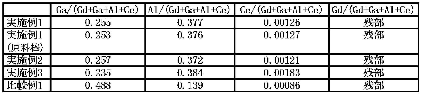


Claims
Priority Applications (6)
| Application Number | Priority Date | Filing Date | Title |
|---|---|---|---|
| JP2006548995A JP5233119B2 (en) | 2004-12-21 | 2005-12-20 | Fluorescent material and manufacturing method thereof, radiation detector using fluorescent material, and X-ray CT apparatus |
| US11/722,413 US7595492B2 (en) | 2004-12-21 | 2005-12-20 | Fluorescent material, a method of manufacturing the fluorescent material, a radiation detector using the fluorescent material, and an X-ray CT scanner |
| EP05820331.6A EP1829950B1 (en) | 2004-12-21 | 2005-12-20 | Fluorescent material and method for preparation thereof, radiation detector using fluorescent material, and x-ray ct device |
| CN200580043772.2A CN101084290B (en) | 2004-12-21 | 2005-12-20 | Fluorescent material and method for preparation thereof, radiation detector using fluorescent material, and x-ray ct device |
| IL183952A IL183952A (en) | 2004-12-21 | 2007-06-14 | Fluorescent material, method of manufacturing the fluorescent material, a radiation detector using the fluorescent material and an x - ray ct scanner |
| US12/379,849 US7947956B2 (en) | 2004-12-21 | 2009-03-03 | Fluorescent material, a method of manufacturing the fluorescent material, a radiation detector using the fluorescent material, and an X-ray CT scanner |
Applications Claiming Priority (4)
| Application Number | Priority Date | Filing Date | Title |
|---|---|---|---|
| JP2004369103 | 2004-12-21 | ||
| JP2004-369103 | 2004-12-21 | ||
| JP2005-053335 | 2005-02-28 | ||
| JP2005053335 | 2005-02-28 |
Related Child Applications (2)
| Application Number | Title | Priority Date | Filing Date |
|---|---|---|---|
| US11/722,413 A-371-Of-International US7595492B2 (en) | 2004-12-21 | 2005-12-20 | Fluorescent material, a method of manufacturing the fluorescent material, a radiation detector using the fluorescent material, and an X-ray CT scanner |
| US12/379,849 Continuation US7947956B2 (en) | 2004-12-21 | 2009-03-03 | Fluorescent material, a method of manufacturing the fluorescent material, a radiation detector using the fluorescent material, and an X-ray CT scanner |
Publications (1)
| Publication Number | Publication Date |
|---|---|
| WO2006068130A1 true WO2006068130A1 (en) | 2006-06-29 |
Family
ID=36601730
Family Applications (1)
| Application Number | Title | Priority Date | Filing Date |
|---|---|---|---|
| PCT/JP2005/023347 WO2006068130A1 (en) | 2004-12-21 | 2005-12-20 | Fluorescent material and method for preparation thereof, radiation detector using fluorescent material, and x-ray ct device |
Country Status (6)
| Country | Link |
|---|---|
| US (2) | US7595492B2 (en) |
| EP (1) | EP1829950B1 (en) |
| JP (2) | JP5233119B2 (en) |
| CN (2) | CN102127440A (en) |
| IL (1) | IL183952A (en) |
| WO (1) | WO2006068130A1 (en) |
Cited By (26)
| Publication number | Priority date | Publication date | Assignee | Title |
|---|---|---|---|---|
| EP2128222A1 (en) * | 2007-02-02 | 2009-12-02 | Hitachi Metals, Ltd. | Fluorescent material, scintillator using the fluorescent material, and radiation detector |
| US20100231892A1 (en) * | 2006-08-15 | 2010-09-16 | Koninklijke Philips Electronics N. V. | Method of measuring and/or judging the afterglow in ceramic materials and detector |
| JP2010261005A (en) * | 2008-07-31 | 2010-11-18 | Hitachi Metals Ltd | Fluorescent material and scintillator and radiation detector using the same |
| JP2011153200A (en) * | 2010-01-27 | 2011-08-11 | Hitachi Metals Ltd | Phosphor material, and scintillator and radiation detector by using the same |
| JP2011207937A (en) * | 2010-03-29 | 2011-10-20 | Hitachi Metals Ltd | Method for producing fluorescent material |
| WO2012057133A1 (en) | 2010-10-29 | 2012-05-03 | 日立金属株式会社 | Polycrystalline scintillator for detecting soft x-rays |
| WO2012105202A1 (en) * | 2011-01-31 | 2012-08-09 | 国立大学法人東北大学 | Garnet type crystal for scintillator and radiation detector using same |
| JP2012180399A (en) * | 2011-02-28 | 2012-09-20 | Furukawa Co Ltd | Garnet-type crystal for scintillator, and radiation detector using the same |
| WO2013005848A1 (en) * | 2011-07-07 | 2013-01-10 | 株式会社東芝 | Photon counting image detector, x-ray diagnosis apparatus, and x-ray computerized tomography apparatus |
| JP2013043960A (en) * | 2011-08-26 | 2013-03-04 | Furukawa Co Ltd | Garnet type crystal for scintillator and radiation detector using the same |
| JP2013253867A (en) * | 2012-06-07 | 2013-12-19 | Furukawa Co Ltd | Radiation detector, food product radiation detector, manufacturing method of radiation detector and radiation detection method |
| JP2014526587A (en) * | 2011-09-22 | 2014-10-06 | サン−ゴバン クリストー エ デテクトゥール | Scintillation compounds containing rare earth elements and formation processes thereof |
| JP2016506977A (en) * | 2013-01-23 | 2016-03-07 | ユニバーシティ オブ テネシー リサーチ ファウンデーション | Co-doping method for modifying the scintillation and optical properties of garnet scintillators |
| JP2016528484A (en) * | 2013-06-14 | 2016-09-15 | ユニバーシティ オブ テネシー リサーチ ファウンデーション | Radiation detector for imaging applications with stabilized light output |
| JP2016538366A (en) * | 2013-12-17 | 2016-12-08 | コーニンクレッカ フィリップス エヌ ヴェKoninklijke Philips N.V. | Garnet scintillator composition |
| JP2017105993A (en) * | 2015-12-01 | 2017-06-15 | シーメンス メディカル ソリューションズ ユーエスエー インコーポレイテッドSiemens Medical Solutions USA,Inc. | Method for controlling gallium content in gadolinium-gallium garnet scintillator |
| JPWO2016021705A1 (en) * | 2014-08-07 | 2017-07-13 | 三菱ケミカル株式会社 | Phosphor, light emitting device, image display device, and illumination device |
| US9868900B2 (en) | 2010-11-16 | 2018-01-16 | Samuel Blahuta | Scintillation compound including a rare earth element and a process of forming the same |
| JP2018124134A (en) * | 2017-01-31 | 2018-08-09 | 三菱ケミカル株式会社 | Ceramic scintillator, scintillator array, radiation detector and radiation inspection device |
| WO2018222078A1 (en) | 2017-06-02 | 2018-12-06 | Открытое акционерное общество "ФОМОС-МАТЕРИАЛС" | Single crystal with garnet structure for scintillation counters and method for producing same |
| US10174247B2 (en) | 2014-05-01 | 2019-01-08 | Tohoku Techno Arch Co., Ltd. | Illuminant and radiation detector |
| JP2020164415A (en) * | 2015-01-09 | 2020-10-08 | フォルシュングスフェアブント・ベルリン・アインゲトラーゲナー・フェライン | METHOD FOR GROWING BETA PHASE OF GALLIUM OXIDE (β-Ga2O3) SINGLE CRYSTALS FROM METAL CONTAINED WITHIN METAL CRUCIBLE |
| CN111875370A (en) * | 2020-07-07 | 2020-11-03 | 中国科学院上海光学精密机械研究所 | Composite crystalline phase fluorescent ceramic for excitation of blue light LED or LD and preparation method thereof |
| JP2021046462A (en) * | 2019-09-17 | 2021-03-25 | 株式会社東芝 | Radiation detecting material and radiation detector |
| US10961452B2 (en) | 2015-12-01 | 2021-03-30 | Siemens Medical Solutions Usa, Inc. | Method for controlling gallium content in gadolinium-gallium garnet scintillators |
| CN115925408A (en) * | 2022-11-18 | 2023-04-07 | 上海御光新材料科技股份有限公司 | Transparent scintillating ceramic material and preparation method and application thereof |
Families Citing this family (38)
| Publication number | Priority date | Publication date | Assignee | Title |
|---|---|---|---|---|
| US7442629B2 (en) | 2004-09-24 | 2008-10-28 | President & Fellows Of Harvard College | Femtosecond laser-induced formation of submicrometer spikes on a semiconductor substrate |
| US7057256B2 (en) | 2001-05-25 | 2006-06-06 | President & Fellows Of Harvard College | Silicon-based visible and near-infrared optoelectric devices |
| JP2007230877A (en) * | 2006-02-27 | 2007-09-13 | Keio Gijuku | Luminescent labeling reagent |
| US8455833B2 (en) * | 2008-09-29 | 2013-06-04 | Hitachi Metals, Ltd. | Single crystal scintillator material, method for producing same, radiation detector and PET system |
| WO2010127298A2 (en) * | 2009-04-30 | 2010-11-04 | Sionyx, Inc. | Low oxygen content semiconductor material for surface enhanced photonic devices associated methods |
| US9673243B2 (en) | 2009-09-17 | 2017-06-06 | Sionyx, Llc | Photosensitive imaging devices and associated methods |
| US9911781B2 (en) | 2009-09-17 | 2018-03-06 | Sionyx, Llc | Photosensitive imaging devices and associated methods |
| US8692198B2 (en) | 2010-04-21 | 2014-04-08 | Sionyx, Inc. | Photosensitive imaging devices and associated methods |
| CN101872831A (en) * | 2010-05-26 | 2010-10-27 | 上海嘉利莱实业有限公司 | Single crystal fluorescent material suitable for white light LED |
| CN106449684B (en) | 2010-06-18 | 2019-09-27 | 西奥尼克斯公司 | High speed photosensitive device and correlation technique |
| US10371831B2 (en) * | 2010-11-04 | 2019-08-06 | Radiation Monitoring Devices, Inc. | Mixed garnet oxide scintillators and corresponding systems and methods |
| US9496308B2 (en) | 2011-06-09 | 2016-11-15 | Sionyx, Llc | Process module for increasing the response of backside illuminated photosensitive imagers and associated methods |
| WO2013010127A2 (en) | 2011-07-13 | 2013-01-17 | Sionyx, Inc. | Biometric imaging devices and associated methods |
| EP2744870B1 (en) * | 2011-08-16 | 2017-11-22 | Nitto Denko Corporation | Phosphor compositions and methods of making the same |
| CN104169392B (en) * | 2012-03-15 | 2016-06-22 | 株式会社东芝 | Solid scintillator, radiation detector and radiation inspecting apparatus |
| US9064764B2 (en) | 2012-03-22 | 2015-06-23 | Sionyx, Inc. | Pixel isolation elements, devices, and associated methods |
| US9145517B2 (en) * | 2012-04-17 | 2015-09-29 | General Electric Company | Rare earth garnet scintillator and method of making same |
| EP3489328A1 (en) * | 2012-11-14 | 2019-05-29 | Koninklijke Philips N.V. | Scintillator material |
| WO2014127376A2 (en) | 2013-02-15 | 2014-08-21 | Sionyx, Inc. | High dynamic range cmos image sensor having anti-blooming properties and associated methods |
| WO2014151093A1 (en) | 2013-03-15 | 2014-09-25 | Sionyx, Inc. | Three dimensional imaging utilizing stacked imager devices and associated methods |
| KR101775186B1 (en) * | 2013-04-05 | 2017-09-05 | 주식회사 엘지화학 | Adhesive composition for touch panel, adhesive film and touch panel |
| WO2014168202A1 (en) * | 2013-04-12 | 2014-10-16 | 日立金属株式会社 | Fluorescent material, scintillator and radiation conversion panel |
| US9209345B2 (en) | 2013-06-29 | 2015-12-08 | Sionyx, Inc. | Shallow trench textured regions and associated methods |
| JP6102687B2 (en) * | 2013-11-12 | 2017-03-29 | 住友金属鉱山株式会社 | Method for producing complex oxide single crystal |
| JP6102686B2 (en) * | 2013-11-12 | 2017-03-29 | 住友金属鉱山株式会社 | Method for producing complex oxide single crystal |
| EP3202874B1 (en) | 2014-09-30 | 2020-07-01 | Hitachi Metals, Ltd. | Fluorescent material, scintillator, scintillator array, and radiation detector |
| CZ2015711A3 (en) * | 2015-10-09 | 2016-10-19 | Crytur Spol S R O | Method of shortening scintillation response of scintillator radiation centers and scintillator material with shortened scintillation response |
| JP6535271B2 (en) * | 2015-11-09 | 2019-06-26 | 浜松ホトニクス株式会社 | Radiation detector and method of manufacturing radiation detector |
| CN105297136A (en) * | 2015-11-13 | 2016-02-03 | 孙雷 | Cerium-doped gadolinium lutecium aluminate garnet crystal for laser illumination and preparation method thereof |
| JP6700737B2 (en) * | 2015-11-20 | 2020-05-27 | キヤノン株式会社 | Radiation imaging system, signal processing device, and signal processing method for radiation image |
| US10150914B2 (en) * | 2015-11-25 | 2018-12-11 | Siemens Medical Solutions Usa, Inc. | Ceramic phoswich with fused optical elements, method of manufacture thereof and articles comprising the same |
| US10000698B2 (en) * | 2016-03-08 | 2018-06-19 | Lawrence Livermore National Security, Llc | Transparent ceramic garnet scintillator detector for positron emission tomography |
| JP2019057071A (en) * | 2017-09-20 | 2019-04-11 | ルネサスエレクトロニクス株式会社 | Semiconductor device and program for use in the semiconductor device |
| JP2019102456A (en) * | 2017-11-30 | 2019-06-24 | ガタン インコーポレイテッドGatan Inc. | High density fast phosphor for electron microscopy |
| RU2682554C1 (en) * | 2017-12-28 | 2019-03-19 | Федеральное государственное унитарное предприятие "Институт химических реактивов и особо чистых химических веществ Национального исследовательского центра "Курчатовский институт" | Poly-crystalline scintillation materials in the form of powders production method |
| KR102634270B1 (en) * | 2018-11-27 | 2024-02-06 | 한국전기연구원 | Intra-oral Radiation Detector of Low-dose and High resolution |
| CN110256073A (en) * | 2019-02-28 | 2019-09-20 | 江苏罗化新材料有限公司 | Ce:GAGG fluorescence ceramics and its preparation preparation method, preparation system |
| EP4039663A1 (en) * | 2021-02-05 | 2022-08-10 | Centre national de la recherche scientifique | Ceramic material with a garnet structure showing a non-stoichiometry, synthesis and uses thereof |
Citations (11)
| Publication number | Priority date | Publication date | Assignee | Title |
|---|---|---|---|---|
| JPH04289483A (en) * | 1990-06-29 | 1992-10-14 | General Electric Co <Ge> | High-speed radioactive ray resisting ct scintillator device using scintillator of garnet structure |
| JPH0920599A (en) * | 1995-07-07 | 1997-01-21 | Mitsubishi Heavy Ind Ltd | Terbium-containing luminescent material and its production |
| JP2001004753A (en) * | 1999-06-23 | 2001-01-12 | Hitachi Medical Corp | Oxide phosphor and radiation detector using it as well as x-ray ct apparatus |
| JP2001183463A (en) * | 1999-12-24 | 2001-07-06 | Hitachi Medical Corp | Scintillator, radiation detector using the same, and x-ray ct equipment |
| JP2001294853A (en) * | 2000-04-12 | 2001-10-23 | Hitachi Medical Corp | Oxide fluorescent substance, radiation detector using the same, and x-ray ct apparatus |
| JP2001303048A (en) * | 2000-04-26 | 2001-10-31 | Hitachi Medical Corp | Fluorescent substance and radiation detector and x-ray ct instrument each using the same |
| JP2002189080A (en) * | 2000-12-21 | 2002-07-05 | Hitachi Medical Corp | Oxide phosphor, radiation detector using the same, and x-ray ct |
| JP2003027057A (en) * | 2001-07-17 | 2003-01-29 | Hitachi Ltd | Light source and image display device using the same |
| JP2004047196A (en) * | 2002-07-10 | 2004-02-12 | Hitachi Ltd | Electron microscope |
| JP2004189783A (en) * | 2002-12-09 | 2004-07-08 | National Institute Of Advanced Industrial & Technology | Luminescent material |
| JP2005095514A (en) * | 2003-09-26 | 2005-04-14 | Hitachi Medical Corp | Radiation detector and x-ray ct apparatus using the same |
Family Cites Families (8)
| Publication number | Priority date | Publication date | Assignee | Title |
|---|---|---|---|---|
| GB1589964A (en) * | 1976-09-03 | 1981-05-20 | Johnson Matthey Co Ltd | Luminescent materials |
| JPS5888699A (en) * | 1981-11-20 | 1983-05-26 | 富士写真フイルム株式会社 | Radiation image conversion panel |
| EP0292616B1 (en) | 1987-05-26 | 1992-05-20 | Agfa-Gevaert N.V. | X-ray conversion into light |
| EP1043383B2 (en) | 1997-12-24 | 2007-05-30 | Hitachi Medical Corporation | Phosphors, and radiation detectors and x-ray ct unit made by using the same |
| US7008558B2 (en) | 2001-10-11 | 2006-03-07 | General Electric Company | Terbium or lutetium containing scintillator compositions having increased resistance to radiation damage |
| JP4087093B2 (en) | 2001-10-15 | 2008-05-14 | 株式会社日立メディコ | Phosphor element, radiation detector using the same, and medical image diagnostic apparatus |
| US7038370B2 (en) * | 2003-03-17 | 2006-05-02 | Lumileds Lighting, U.S., Llc | Phosphor converted light emitting device |
| JP4973189B2 (en) * | 2004-10-19 | 2012-07-11 | 日亜化学工業株式会社 | Semiconductor element |
-
2005
- 2005-12-20 JP JP2006548995A patent/JP5233119B2/en active Active
- 2005-12-20 EP EP05820331.6A patent/EP1829950B1/en active Active
- 2005-12-20 CN CN201010591247.7A patent/CN102127440A/en active Pending
- 2005-12-20 US US11/722,413 patent/US7595492B2/en active Active
- 2005-12-20 CN CN200580043772.2A patent/CN101084290B/en active Active
- 2005-12-20 WO PCT/JP2005/023347 patent/WO2006068130A1/en active Application Filing
-
2007
- 2007-06-14 IL IL183952A patent/IL183952A/en active IP Right Grant
-
2009
- 2009-03-03 US US12/379,849 patent/US7947956B2/en active Active
-
2012
- 2012-05-24 JP JP2012118561A patent/JP5729352B2/en active Active
Patent Citations (11)
| Publication number | Priority date | Publication date | Assignee | Title |
|---|---|---|---|---|
| JPH04289483A (en) * | 1990-06-29 | 1992-10-14 | General Electric Co <Ge> | High-speed radioactive ray resisting ct scintillator device using scintillator of garnet structure |
| JPH0920599A (en) * | 1995-07-07 | 1997-01-21 | Mitsubishi Heavy Ind Ltd | Terbium-containing luminescent material and its production |
| JP2001004753A (en) * | 1999-06-23 | 2001-01-12 | Hitachi Medical Corp | Oxide phosphor and radiation detector using it as well as x-ray ct apparatus |
| JP2001183463A (en) * | 1999-12-24 | 2001-07-06 | Hitachi Medical Corp | Scintillator, radiation detector using the same, and x-ray ct equipment |
| JP2001294853A (en) * | 2000-04-12 | 2001-10-23 | Hitachi Medical Corp | Oxide fluorescent substance, radiation detector using the same, and x-ray ct apparatus |
| JP2001303048A (en) * | 2000-04-26 | 2001-10-31 | Hitachi Medical Corp | Fluorescent substance and radiation detector and x-ray ct instrument each using the same |
| JP2002189080A (en) * | 2000-12-21 | 2002-07-05 | Hitachi Medical Corp | Oxide phosphor, radiation detector using the same, and x-ray ct |
| JP2003027057A (en) * | 2001-07-17 | 2003-01-29 | Hitachi Ltd | Light source and image display device using the same |
| JP2004047196A (en) * | 2002-07-10 | 2004-02-12 | Hitachi Ltd | Electron microscope |
| JP2004189783A (en) * | 2002-12-09 | 2004-07-08 | National Institute Of Advanced Industrial & Technology | Luminescent material |
| JP2005095514A (en) * | 2003-09-26 | 2005-04-14 | Hitachi Medical Corp | Radiation detector and x-ray ct apparatus using the same |
Non-Patent Citations (1)
| Title |
|---|
| See also references of EP1829950A4 * |
Cited By (48)
| Publication number | Priority date | Publication date | Assignee | Title |
|---|---|---|---|---|
| US20100231892A1 (en) * | 2006-08-15 | 2010-09-16 | Koninklijke Philips Electronics N. V. | Method of measuring and/or judging the afterglow in ceramic materials and detector |
| EP2128222A1 (en) * | 2007-02-02 | 2009-12-02 | Hitachi Metals, Ltd. | Fluorescent material, scintillator using the fluorescent material, and radiation detector |
| JPWO2008093869A1 (en) * | 2007-02-02 | 2010-05-20 | 日立金属株式会社 | Fluorescent material, scintillator and radiation detector using the same |
| EP2128222A4 (en) * | 2007-02-02 | 2011-09-14 | Hitachi Metals Ltd | Fluorescent material, scintillator using the fluorescent material, and radiation detector |
| JP5212115B2 (en) * | 2007-02-02 | 2013-06-19 | 日立金属株式会社 | Fluorescent material, scintillator and radiation detector using the same |
| US8410446B2 (en) | 2007-02-02 | 2013-04-02 | Hitachi Metals, Ltd. | Fluorescent material, scintillator using same, and radiation detector using same |
| JP2010261005A (en) * | 2008-07-31 | 2010-11-18 | Hitachi Metals Ltd | Fluorescent material and scintillator and radiation detector using the same |
| JP2011153200A (en) * | 2010-01-27 | 2011-08-11 | Hitachi Metals Ltd | Phosphor material, and scintillator and radiation detector by using the same |
| JP2011207937A (en) * | 2010-03-29 | 2011-10-20 | Hitachi Metals Ltd | Method for producing fluorescent material |
| JP5633573B2 (en) * | 2010-10-29 | 2014-12-03 | 日立金属株式会社 | Polycrystalline scintillator for soft X-ray detection |
| CN102869748A (en) * | 2010-10-29 | 2013-01-09 | 日立金属株式会社 | Polycrystalline scintillator for detecting soft x-rays |
| US8815122B2 (en) | 2010-10-29 | 2014-08-26 | Hitachi Metals, Ltd. | Polycrystalline scintillator for detecting soft X-rays |
| CN102869748B (en) * | 2010-10-29 | 2015-01-07 | 日立金属株式会社 | Polycrystalline scintillator for detecting soft x-rays and manufacturing method |
| JPWO2012057133A1 (en) * | 2010-10-29 | 2014-05-12 | 日立金属株式会社 | Polycrystalline scintillator for soft X-ray detection |
| WO2012057133A1 (en) | 2010-10-29 | 2012-05-03 | 日立金属株式会社 | Polycrystalline scintillator for detecting soft x-rays |
| US10907096B2 (en) | 2010-11-16 | 2021-02-02 | Saint-Gobain Cristaux & Detecteurs | Scintillation compound including a rare earth element and a process of forming the same |
| US9868900B2 (en) | 2010-11-16 | 2018-01-16 | Samuel Blahuta | Scintillation compound including a rare earth element and a process of forming the same |
| US10647916B2 (en) | 2010-11-16 | 2020-05-12 | Saint-Gobain Cristaux Et Detecteurs | Scintillation compound including a rare earth element in a tetravalent state |
| US11926777B2 (en) | 2010-11-16 | 2024-03-12 | Luxium Solutions, Llc | Scintillation compound including a rare earth element and a process of forming the same |
| JPWO2012105202A1 (en) * | 2011-01-31 | 2014-07-03 | 古河機械金属株式会社 | Garnet-type crystal for scintillator and radiation detector using the same |
| JP5952746B2 (en) * | 2011-01-31 | 2016-07-13 | 古河機械金属株式会社 | Garnet-type single crystal for scintillator and radiation detector using the same |
| WO2012105202A1 (en) * | 2011-01-31 | 2012-08-09 | 国立大学法人東北大学 | Garnet type crystal for scintillator and radiation detector using same |
| US8969812B2 (en) | 2011-01-31 | 2015-03-03 | Furukawa Co., Ltd. | Garnet-type crystal for scintillator and radiation detector using the same |
| JP2012180399A (en) * | 2011-02-28 | 2012-09-20 | Furukawa Co Ltd | Garnet-type crystal for scintillator, and radiation detector using the same |
| US9213108B2 (en) | 2011-07-07 | 2015-12-15 | Kabushiki Kaisha Toshiba | Photon counting type image detector, X-ray diagnosis apparatus and X-ray computed tomography apparatus |
| WO2013005848A1 (en) * | 2011-07-07 | 2013-01-10 | 株式会社東芝 | Photon counting image detector, x-ray diagnosis apparatus, and x-ray computerized tomography apparatus |
| JP2013019698A (en) * | 2011-07-07 | 2013-01-31 | Toshiba Corp | Photon count type image detector, x-ray diagnostic device, and x-ray computer tomographic device |
| JP2013043960A (en) * | 2011-08-26 | 2013-03-04 | Furukawa Co Ltd | Garnet type crystal for scintillator and radiation detector using the same |
| JP2014526587A (en) * | 2011-09-22 | 2014-10-06 | サン−ゴバン クリストー エ デテクトゥール | Scintillation compounds containing rare earth elements and formation processes thereof |
| JP2013253867A (en) * | 2012-06-07 | 2013-12-19 | Furukawa Co Ltd | Radiation detector, food product radiation detector, manufacturing method of radiation detector and radiation detection method |
| JP2016506977A (en) * | 2013-01-23 | 2016-03-07 | ユニバーシティ オブ テネシー リサーチ ファウンデーション | Co-doping method for modifying the scintillation and optical properties of garnet scintillators |
| JP2016528484A (en) * | 2013-06-14 | 2016-09-15 | ユニバーシティ オブ テネシー リサーチ ファウンデーション | Radiation detector for imaging applications with stabilized light output |
| JP2016538366A (en) * | 2013-12-17 | 2016-12-08 | コーニンクレッカ フィリップス エヌ ヴェKoninklijke Philips N.V. | Garnet scintillator composition |
| US10174247B2 (en) | 2014-05-01 | 2019-01-08 | Tohoku Techno Arch Co., Ltd. | Illuminant and radiation detector |
| JPWO2016021705A1 (en) * | 2014-08-07 | 2017-07-13 | 三菱ケミカル株式会社 | Phosphor, light emitting device, image display device, and illumination device |
| JP2020164415A (en) * | 2015-01-09 | 2020-10-08 | フォルシュングスフェアブント・ベルリン・アインゲトラーゲナー・フェライン | METHOD FOR GROWING BETA PHASE OF GALLIUM OXIDE (β-Ga2O3) SINGLE CRYSTALS FROM METAL CONTAINED WITHIN METAL CRUCIBLE |
| JP7046117B2 (en) | 2015-01-09 | 2022-04-01 | フォルシュングスフェアブント・ベルリン・アインゲトラーゲナー・フェライン | A method for growing a beta-phase gallium oxide (β-Ga2O3) single crystal from a metal contained in a metal crucible. |
| JP7438689B2 (en) | 2015-12-01 | 2024-02-27 | シーメンス メディカル ソリューションズ ユーエスエー インコーポレイテッド | Method for producing a garnet crystal scintillator containing gadolinium-gallium |
| JP2020007554A (en) * | 2015-12-01 | 2020-01-16 | シーメンス メディカル ソリューションズ ユーエスエー インコーポレイテッドSiemens Medical Solutions USA,Inc. | Method for manufacturing gadolinium-gallium-containing garnet crystal scintillators |
| JP2017105993A (en) * | 2015-12-01 | 2017-06-15 | シーメンス メディカル ソリューションズ ユーエスエー インコーポレイテッドSiemens Medical Solutions USA,Inc. | Method for controlling gallium content in gadolinium-gallium garnet scintillator |
| US10197685B2 (en) | 2015-12-01 | 2019-02-05 | Siemens Medical Solutions Usa, Inc. | Method for controlling gallium content in gadolinium-gallium garnet scintillators |
| US10961452B2 (en) | 2015-12-01 | 2021-03-30 | Siemens Medical Solutions Usa, Inc. | Method for controlling gallium content in gadolinium-gallium garnet scintillators |
| JP2018124134A (en) * | 2017-01-31 | 2018-08-09 | 三菱ケミカル株式会社 | Ceramic scintillator, scintillator array, radiation detector and radiation inspection device |
| WO2018222078A1 (en) | 2017-06-02 | 2018-12-06 | Открытое акционерное общество "ФОМОС-МАТЕРИАЛС" | Single crystal with garnet structure for scintillation counters and method for producing same |
| JP2021046462A (en) * | 2019-09-17 | 2021-03-25 | 株式会社東芝 | Radiation detecting material and radiation detector |
| CN111875370A (en) * | 2020-07-07 | 2020-11-03 | 中国科学院上海光学精密机械研究所 | Composite crystalline phase fluorescent ceramic for excitation of blue light LED or LD and preparation method thereof |
| CN115925408A (en) * | 2022-11-18 | 2023-04-07 | 上海御光新材料科技股份有限公司 | Transparent scintillating ceramic material and preparation method and application thereof |
| CN115925408B (en) * | 2022-11-18 | 2024-04-12 | 上海御光新材料科技股份有限公司 | Transparent scintillating ceramic material and preparation method and application thereof |
Also Published As
| Publication number | Publication date |
|---|---|
| US7595492B2 (en) | 2009-09-29 |
| JP2012177134A (en) | 2012-09-13 |
| US20090261255A1 (en) | 2009-10-22 |
| US7947956B2 (en) | 2011-05-24 |
| CN101084290B (en) | 2012-07-18 |
| EP1829950A4 (en) | 2010-03-10 |
| CN102127440A (en) | 2011-07-20 |
| JPWO2006068130A1 (en) | 2008-06-12 |
| US20080017802A1 (en) | 2008-01-24 |
| IL183952A0 (en) | 2007-10-31 |
| EP1829950B1 (en) | 2017-04-05 |
| JP5729352B2 (en) | 2015-06-03 |
| JP5233119B2 (en) | 2013-07-10 |
| CN101084290A (en) | 2007-12-05 |
| EP1829950A1 (en) | 2007-09-05 |
| IL183952A (en) | 2014-05-28 |
Similar Documents
| Publication | Publication Date | Title |
|---|---|---|
| WO2006068130A1 (en) | Fluorescent material and method for preparation thereof, radiation detector using fluorescent material, and x-ray ct device | |
| JP5212115B2 (en) | Fluorescent material, scintillator and radiation detector using the same | |
| JP5521412B2 (en) | Fluorescent material, scintillator and radiation detector using the same | |
| US9193903B2 (en) | Solid scintillator, radiation detector, and radiation examination device | |
| JP5633573B2 (en) | Polycrystalline scintillator for soft X-ray detection | |
| JP5035660B2 (en) | Fluorescent material and radiation detector using the same | |
| US4473513A (en) | Method for sintering high density yttria-gadolinia ceramic scintillators | |
| JP5686724B2 (en) | Solid scintillator, radiation detector, and X-ray tomography apparatus | |
| JP5311241B2 (en) | Polycrystalline scintillator, manufacturing method thereof, and radiation detector | |
| JP5505782B2 (en) | Fluorescent material, scintillator and radiation detector using the same | |
| EP0097296B1 (en) | Rare earth doped yttria-gadolinia ceramic scintillators and methods for making | |
| JP4692890B2 (en) | Fluorescent material and radiation detector using the same | |
| WO2022202500A1 (en) | Scintillator and radiation detector | |
| JP2001181043A (en) | Transparent polycrystalline garnet scintillator, powder for scintillator and method for producing the same | |
| WO2021132494A1 (en) | Scintillator and radiation detector | |
| WO2021149670A1 (en) | Scintillator and radiation detector | |
| JP2022158438A (en) | OXIDE CRYSTAL MATERIAL, PHOSPHOR MATERIAL, DEVICE INCLUDING THE PHOSPHOR MATERIAL, AND Li ION CONDUCTOR INCLUDING THE OXIDE CRYSTAL MATERIAL | |
| JP2016164210A (en) | Scintillator material, radiation detector, and radiation inspection device |
Legal Events
| Date | Code | Title | Description |
|---|---|---|---|
| AK | Designated states |
Kind code of ref document: A1 Designated state(s): AE AG AL AM AT AU AZ BA BB BG BR BW BY BZ CA CH CN CO CR CU CZ DE DK DM DZ EC EE EG ES FI GB GD GE GH GM HR HU ID IL IN IS JP KE KG KM KN KP KR KZ LC LK LR LS LT LU LV LY MA MD MG MK MN MW MX MZ NA NG NI NO NZ OM PG PH PL PT RO RU SC SD SE SG SK SL SM SY TJ TM TN TR TT TZ UA UG US UZ VC VN YU ZA ZM ZW |
|
| AL | Designated countries for regional patents |
Kind code of ref document: A1 Designated state(s): BW GH GM KE LS MW MZ NA SD SL SZ TZ UG ZM ZW AM AZ BY KG KZ MD RU TJ TM AT BE BG CH CY CZ DE DK EE ES FI FR GB GR HU IE IS IT LT LU LV MC NL PL PT RO SE SI SK TR BF BJ CF CG CI CM GA GN GQ GW ML MR NE SN TD TG |
|
| 121 | Ep: the epo has been informed by wipo that ep was designated in this application | ||
| WWE | Wipo information: entry into national phase |
Ref document number: 183952 Country of ref document: IL |
|
| REEP | Request for entry into the european phase |
Ref document number: 2005820331 Country of ref document: EP |
|
| WWE | Wipo information: entry into national phase |
Ref document number: 2005820331 Country of ref document: EP |
|
| WWE | Wipo information: entry into national phase |
Ref document number: 2006548995 Country of ref document: JP |
|
| WWE | Wipo information: entry into national phase |
Ref document number: 200580043772.2 Country of ref document: CN |
|
| WWE | Wipo information: entry into national phase |
Ref document number: 11722413 Country of ref document: US |
|
| NENP | Non-entry into the national phase |
Ref country code: DE |
|
| WWP | Wipo information: published in national office |
Ref document number: 2005820331 Country of ref document: EP |
|
| WWP | Wipo information: published in national office |
Ref document number: 183952 Country of ref document: IL |
|
| WWP | Wipo information: published in national office |
Ref document number: 11722413 Country of ref document: US |