WO2005092901A1 - Novel compound and organic electronic device using such compound - Google Patents
Novel compound and organic electronic device using such compound Download PDFInfo
- Publication number
- WO2005092901A1 WO2005092901A1 PCT/JP2005/005979 JP2005005979W WO2005092901A1 WO 2005092901 A1 WO2005092901 A1 WO 2005092901A1 JP 2005005979 W JP2005005979 W JP 2005005979W WO 2005092901 A1 WO2005092901 A1 WO 2005092901A1
- Authority
- WO
- WIPO (PCT)
- Prior art keywords
- group
- organic
- layer
- substituted
- compound
- Prior art date
Links
- 150000001875 compounds Chemical class 0.000 title claims abstract description 121
- 125000000962 organic group Chemical group 0.000 claims abstract description 34
- 125000004435 hydrogen atom Chemical group [H]* 0.000 claims abstract description 21
- 125000004430 oxygen atom Chemical group O* 0.000 claims abstract description 13
- 229910052717 sulfur Inorganic materials 0.000 claims abstract description 13
- 125000004434 sulfur atom Chemical group 0.000 claims abstract description 13
- 125000005647 linker group Chemical group 0.000 claims abstract description 8
- 125000000217 alkyl group Chemical group 0.000 claims description 57
- 108091008695 photoreceptors Proteins 0.000 claims description 48
- 125000003118 aryl group Chemical group 0.000 claims description 38
- 229910052757 nitrogen Inorganic materials 0.000 claims description 26
- 125000000753 cycloalkyl group Chemical group 0.000 claims description 14
- 239000000126 substance Substances 0.000 claims description 14
- 125000003710 aryl alkyl group Chemical group 0.000 claims description 11
- 125000004429 atom Chemical group 0.000 claims description 10
- 150000000000 tetracarboxylic acids Chemical class 0.000 claims description 10
- XLYOFNOQVPJJNP-UHFFFAOYSA-N water Substances O XLYOFNOQVPJJNP-UHFFFAOYSA-N 0.000 claims description 10
- IJGRMHOSHXDMSA-UHFFFAOYSA-N nitrogen Substances N#N IJGRMHOSHXDMSA-UHFFFAOYSA-N 0.000 claims description 6
- QJGQUHMNIGDVPM-UHFFFAOYSA-N nitrogen group Chemical group [N] QJGQUHMNIGDVPM-UHFFFAOYSA-N 0.000 claims description 4
- 125000005346 substituted cycloalkyl group Chemical group 0.000 claims 1
- 239000000463 material Substances 0.000 abstract description 110
- 230000035945 sensitivity Effects 0.000 abstract description 9
- 239000010410 layer Substances 0.000 description 253
- UFWIBTONFRDIAS-UHFFFAOYSA-N Naphthalene Chemical compound C1=CC=CC2=CC=CC=C21 UFWIBTONFRDIAS-UHFFFAOYSA-N 0.000 description 140
- -1 benzenetetracarboxylic diimide compound Chemical class 0.000 description 133
- 125000004432 carbon atom Chemical group C* 0.000 description 88
- YXFVVABEGXRONW-UHFFFAOYSA-N Toluene Chemical compound CC1=CC=CC=C1 YXFVVABEGXRONW-UHFFFAOYSA-N 0.000 description 81
- 238000000034 method Methods 0.000 description 64
- ZMXDDKWLCZADIW-UHFFFAOYSA-N N,N-Dimethylformamide Chemical compound CN(C)C=O ZMXDDKWLCZADIW-UHFFFAOYSA-N 0.000 description 63
- OKKJLVBELUTLKV-UHFFFAOYSA-N Methanol Chemical compound OC OKKJLVBELUTLKV-UHFFFAOYSA-N 0.000 description 57
- 239000010409 thin film Substances 0.000 description 56
- 239000004065 semiconductor Substances 0.000 description 53
- 229920005989 resin Polymers 0.000 description 51
- 239000011347 resin Substances 0.000 description 51
- 238000002347 injection Methods 0.000 description 50
- 239000007924 injection Substances 0.000 description 50
- 239000000758 substrate Substances 0.000 description 44
- 239000011230 binding agent Substances 0.000 description 42
- 238000000576 coating method Methods 0.000 description 40
- 239000010408 film Substances 0.000 description 37
- 230000006870 function Effects 0.000 description 31
- GTDPSWPPOUPBNX-UHFFFAOYSA-N ac1mqpva Chemical compound CC12C(=O)OC(=O)C1(C)C1(C)C2(C)C(=O)OC1=O GTDPSWPPOUPBNX-UHFFFAOYSA-N 0.000 description 29
- XAGFODPZIPBFFR-UHFFFAOYSA-N aluminium Chemical compound [Al] XAGFODPZIPBFFR-UHFFFAOYSA-N 0.000 description 27
- 230000015572 biosynthetic process Effects 0.000 description 27
- VLKZOEOYAKHREP-UHFFFAOYSA-N n-Hexane Chemical compound CCCCCC VLKZOEOYAKHREP-UHFFFAOYSA-N 0.000 description 27
- 239000000243 solution Substances 0.000 description 27
- 229910052782 aluminium Inorganic materials 0.000 description 26
- 239000000203 mixture Substances 0.000 description 26
- 238000010992 reflux Methods 0.000 description 26
- 239000002904 solvent Substances 0.000 description 26
- 239000011248 coating agent Substances 0.000 description 25
- 239000013078 crystal Substances 0.000 description 25
- 238000001816 cooling Methods 0.000 description 24
- 239000002356 single layer Substances 0.000 description 24
- 238000003786 synthesis reaction Methods 0.000 description 22
- KFZMGEQAYNKOFK-UHFFFAOYSA-N Isopropanol Chemical compound CC(C)O KFZMGEQAYNKOFK-UHFFFAOYSA-N 0.000 description 20
- 239000000049 pigment Substances 0.000 description 20
- 125000001424 substituent group Chemical group 0.000 description 19
- 239000003795 chemical substances by application Substances 0.000 description 18
- 229910052751 metal Inorganic materials 0.000 description 18
- 239000002184 metal Substances 0.000 description 18
- IEQIEDJGQAUEQZ-UHFFFAOYSA-N phthalocyanine Chemical compound N1C(N=C2C3=CC=CC=C3C(N=C3C4=CC=CC=C4C(=N4)N3)=N2)=C(C=CC=C2)C2=C1N=C1C2=CC=CC=C2C4=N1 IEQIEDJGQAUEQZ-UHFFFAOYSA-N 0.000 description 18
- CSCPPACGZOOCGX-UHFFFAOYSA-N Acetone Chemical compound CC(C)=O CSCPPACGZOOCGX-UHFFFAOYSA-N 0.000 description 17
- 239000002019 doping agent Substances 0.000 description 17
- 230000002829 reductive effect Effects 0.000 description 17
- 239000000047 product Substances 0.000 description 16
- 125000005843 halogen group Chemical group 0.000 description 15
- VYPSYNLAJGMNEJ-UHFFFAOYSA-N Silicium dioxide Chemical compound O=[Si]=O VYPSYNLAJGMNEJ-UHFFFAOYSA-N 0.000 description 14
- 125000006615 aromatic heterocyclic group Chemical group 0.000 description 14
- 238000006243 chemical reaction Methods 0.000 description 14
- 229910052731 fluorine Inorganic materials 0.000 description 14
- 239000011777 magnesium Substances 0.000 description 14
- YTVNOVQHSGMMOV-UHFFFAOYSA-N naphthalenetetracarboxylic dianhydride Chemical compound C1=CC(C(=O)OC2=O)=C3C2=CC=C2C(=O)OC(=O)C1=C32 YTVNOVQHSGMMOV-UHFFFAOYSA-N 0.000 description 14
- 238000010898 silica gel chromatography Methods 0.000 description 14
- FYYHWMGAXLPEAU-UHFFFAOYSA-N Magnesium Chemical compound [Mg] FYYHWMGAXLPEAU-UHFFFAOYSA-N 0.000 description 13
- 125000003545 alkoxy group Chemical group 0.000 description 13
- 238000003756 stirring Methods 0.000 description 13
- UHOVQNZJYSORNB-UHFFFAOYSA-N Benzene Chemical compound C1=CC=CC=C1 UHOVQNZJYSORNB-UHFFFAOYSA-N 0.000 description 12
- OAKJQQAXSVQMHS-UHFFFAOYSA-N Hydrazine Chemical compound NN OAKJQQAXSVQMHS-UHFFFAOYSA-N 0.000 description 12
- 229910045601 alloy Inorganic materials 0.000 description 12
- 239000000956 alloy Substances 0.000 description 12
- MWPLVEDNUUSJAV-UHFFFAOYSA-N anthracene Chemical compound C1=CC=CC2=CC3=CC=CC=C3C=C21 MWPLVEDNUUSJAV-UHFFFAOYSA-N 0.000 description 12
- 229910052801 chlorine Inorganic materials 0.000 description 12
- 125000001309 chloro group Chemical group Cl* 0.000 description 12
- 238000000434 field desorption mass spectrometry Methods 0.000 description 12
- 125000001153 fluoro group Chemical group F* 0.000 description 12
- 238000004519 manufacturing process Methods 0.000 description 12
- 238000002844 melting Methods 0.000 description 12
- 230000008018 melting Effects 0.000 description 12
- BASFCYQUMIYNBI-UHFFFAOYSA-N platinum Chemical compound [Pt] BASFCYQUMIYNBI-UHFFFAOYSA-N 0.000 description 12
- BQCADISMDOOEFD-UHFFFAOYSA-N Silver Chemical compound [Ag] BQCADISMDOOEFD-UHFFFAOYSA-N 0.000 description 11
- 125000002723 alicyclic group Chemical group 0.000 description 11
- 230000005525 hole transport Effects 0.000 description 11
- 238000004949 mass spectrometry Methods 0.000 description 11
- 239000004332 silver Substances 0.000 description 11
- 229910052709 silver Inorganic materials 0.000 description 11
- 238000004544 sputter deposition Methods 0.000 description 11
- HEDRZPFGACZZDS-UHFFFAOYSA-N Chloroform Chemical compound ClC(Cl)Cl HEDRZPFGACZZDS-UHFFFAOYSA-N 0.000 description 10
- 125000001931 aliphatic group Chemical group 0.000 description 10
- 239000004020 conductor Substances 0.000 description 10
- 239000007772 electrode material Substances 0.000 description 10
- 238000011156 evaluation Methods 0.000 description 10
- 238000001914 filtration Methods 0.000 description 10
- 229910052749 magnesium Inorganic materials 0.000 description 10
- 125000002080 perylenyl group Chemical group C1(=CC=C2C=CC=C3C4=CC=CC5=CC=CC(C1=C23)=C45)* 0.000 description 10
- 229920000642 polymer Polymers 0.000 description 10
- 230000008569 process Effects 0.000 description 10
- ODHXBMXNKOYIBV-UHFFFAOYSA-N triphenylamine Chemical compound C1=CC=CC=C1N(C=1C=CC=CC=1)C1=CC=CC=C1 ODHXBMXNKOYIBV-UHFFFAOYSA-N 0.000 description 10
- 238000001771 vacuum deposition Methods 0.000 description 10
- ZWEHNKRNPOVVGH-UHFFFAOYSA-N 2-Butanone Chemical compound CCC(C)=O ZWEHNKRNPOVVGH-UHFFFAOYSA-N 0.000 description 9
- QTBSBXVTEAMEQO-UHFFFAOYSA-N Acetic acid Chemical compound CC(O)=O QTBSBXVTEAMEQO-UHFFFAOYSA-N 0.000 description 9
- YMWUJEATGCHHMB-UHFFFAOYSA-N Dichloromethane Chemical compound ClCCl YMWUJEATGCHHMB-UHFFFAOYSA-N 0.000 description 9
- XEKOWRVHYACXOJ-UHFFFAOYSA-N Ethyl acetate Chemical compound CCOC(C)=O XEKOWRVHYACXOJ-UHFFFAOYSA-N 0.000 description 9
- 125000004414 alkyl thio group Chemical group 0.000 description 9
- 229910052799 carbon Inorganic materials 0.000 description 9
- 239000004417 polycarbonate Substances 0.000 description 9
- 229920000515 polycarbonate Polymers 0.000 description 9
- 239000011241 protective layer Substances 0.000 description 9
- 238000000746 purification Methods 0.000 description 9
- 239000013076 target substance Substances 0.000 description 9
- OKTJSMMVPCPJKN-UHFFFAOYSA-N Carbon Chemical compound [C] OKTJSMMVPCPJKN-UHFFFAOYSA-N 0.000 description 8
- IAZDPXIOMUYVGZ-UHFFFAOYSA-N Dimethylsulphoxide Chemical compound CS(C)=O IAZDPXIOMUYVGZ-UHFFFAOYSA-N 0.000 description 8
- PXHVJJICTQNCMI-UHFFFAOYSA-N Nickel Chemical compound [Ni] PXHVJJICTQNCMI-UHFFFAOYSA-N 0.000 description 8
- WYURNTSHIVDZCO-UHFFFAOYSA-N Tetrahydrofuran Chemical compound C1CCOC1 WYURNTSHIVDZCO-UHFFFAOYSA-N 0.000 description 8
- 125000004183 alkoxy alkyl group Chemical group 0.000 description 8
- 229920001940 conductive polymer Polymers 0.000 description 8
- 239000006185 dispersion Substances 0.000 description 8
- 239000011521 glass Substances 0.000 description 8
- 239000012212 insulator Substances 0.000 description 8
- 229910052744 lithium Inorganic materials 0.000 description 8
- 150000002894 organic compounds Chemical class 0.000 description 8
- WHXSMMKQMYFTQS-UHFFFAOYSA-N Lithium Chemical compound [Li] WHXSMMKQMYFTQS-UHFFFAOYSA-N 0.000 description 7
- CTQNGGLPUBDAKN-UHFFFAOYSA-N O-Xylene Chemical compound CC1=CC=CC=C1C CTQNGGLPUBDAKN-UHFFFAOYSA-N 0.000 description 7
- 239000004952 Polyamide Substances 0.000 description 7
- 239000010931 gold Substances 0.000 description 7
- 229910052740 iodine Inorganic materials 0.000 description 7
- 229910044991 metal oxide Inorganic materials 0.000 description 7
- 150000004706 metal oxides Chemical class 0.000 description 7
- 125000002496 methyl group Chemical group [H]C([H])([H])* 0.000 description 7
- 239000011368 organic material Substances 0.000 description 7
- 229920002647 polyamide Polymers 0.000 description 7
- 229920000728 polyester Polymers 0.000 description 7
- 239000008096 xylene Substances 0.000 description 7
- ZCYVEMRRCGMTRW-UHFFFAOYSA-N 7553-56-2 Chemical group [I] ZCYVEMRRCGMTRW-UHFFFAOYSA-N 0.000 description 6
- WKBOTKDWSSQWDR-UHFFFAOYSA-N Bromine atom Chemical group [Br] WKBOTKDWSSQWDR-UHFFFAOYSA-N 0.000 description 6
- LYCAIKOWRPUZTN-UHFFFAOYSA-N Ethylene glycol Chemical compound OCCO LYCAIKOWRPUZTN-UHFFFAOYSA-N 0.000 description 6
- YLQBMQCUIZJEEH-UHFFFAOYSA-N Furan Chemical compound C=1C=COC=1 YLQBMQCUIZJEEH-UHFFFAOYSA-N 0.000 description 6
- XEEYBQQBJWHFJM-UHFFFAOYSA-N Iron Chemical compound [Fe] XEEYBQQBJWHFJM-UHFFFAOYSA-N 0.000 description 6
- LRHPLDYGYMQRHN-UHFFFAOYSA-N N-Butanol Chemical compound CCCCO LRHPLDYGYMQRHN-UHFFFAOYSA-N 0.000 description 6
- KDLHZDBZIXYQEI-UHFFFAOYSA-N Palladium Chemical compound [Pd] KDLHZDBZIXYQEI-UHFFFAOYSA-N 0.000 description 6
- 239000004793 Polystyrene Substances 0.000 description 6
- XUIMIQQOPSSXEZ-UHFFFAOYSA-N Silicon Chemical compound [Si] XUIMIQQOPSSXEZ-UHFFFAOYSA-N 0.000 description 6
- GWEVSGVZZGPLCZ-UHFFFAOYSA-N Titan oxide Chemical compound O=[Ti]=O GWEVSGVZZGPLCZ-UHFFFAOYSA-N 0.000 description 6
- 230000000903 blocking effect Effects 0.000 description 6
- 239000000969 carrier Substances 0.000 description 6
- MVPPADPHJFYWMZ-UHFFFAOYSA-N chlorobenzene Chemical compound ClC1=CC=CC=C1 MVPPADPHJFYWMZ-UHFFFAOYSA-N 0.000 description 6
- JHIVVAPYMSGYDF-UHFFFAOYSA-N cyclohexanone Chemical compound O=C1CCCCC1 JHIVVAPYMSGYDF-UHFFFAOYSA-N 0.000 description 6
- 238000000151 deposition Methods 0.000 description 6
- 238000003618 dip coating Methods 0.000 description 6
- 230000000694 effects Effects 0.000 description 6
- 230000005684 electric field Effects 0.000 description 6
- 239000010419 fine particle Substances 0.000 description 6
- PCHJSUWPFVWCPO-UHFFFAOYSA-N gold Chemical compound [Au] PCHJSUWPFVWCPO-UHFFFAOYSA-N 0.000 description 6
- 229910052737 gold Inorganic materials 0.000 description 6
- 238000010438 heat treatment Methods 0.000 description 6
- 229910052738 indium Inorganic materials 0.000 description 6
- APFVFJFRJDLVQX-UHFFFAOYSA-N indium atom Chemical compound [In] APFVFJFRJDLVQX-UHFFFAOYSA-N 0.000 description 6
- 238000002156 mixing Methods 0.000 description 6
- 150000004682 monohydrates Chemical class 0.000 description 6
- 125000004108 n-butyl group Chemical group [H]C([H])([H])C([H])([H])C([H])([H])C([H])([H])* 0.000 description 6
- 125000004433 nitrogen atom Chemical group N* 0.000 description 6
- CSHWQDPOILHKBI-UHFFFAOYSA-N peryrene Natural products C1=CC(C2=CC=CC=3C2=C2C=CC=3)=C3C2=CC=CC3=C1 CSHWQDPOILHKBI-UHFFFAOYSA-N 0.000 description 6
- 229910052697 platinum Inorganic materials 0.000 description 6
- 229920000172 poly(styrenesulfonic acid) Polymers 0.000 description 6
- 229920002492 poly(sulfone) Polymers 0.000 description 6
- 229920002223 polystyrene Polymers 0.000 description 6
- 229940005642 polystyrene sulfonic acid Drugs 0.000 description 6
- 229920000123 polythiophene Polymers 0.000 description 6
- 238000002360 preparation method Methods 0.000 description 6
- 229910052710 silicon Inorganic materials 0.000 description 6
- 239000010703 silicon Substances 0.000 description 6
- 238000004528 spin coating Methods 0.000 description 6
- 238000007738 vacuum evaporation Methods 0.000 description 6
- 238000007740 vapor deposition Methods 0.000 description 6
- 229920001609 Poly(3,4-ethylenedioxythiophene) Polymers 0.000 description 5
- 239000004642 Polyimide Substances 0.000 description 5
- 125000004103 aminoalkyl group Chemical group 0.000 description 5
- 238000005266 casting Methods 0.000 description 5
- 230000008021 deposition Effects 0.000 description 5
- 125000001495 ethyl group Chemical group [H]C([H])([H])C([H])([H])* 0.000 description 5
- 238000001704 evaporation Methods 0.000 description 5
- RBTKNAXYKSUFRK-UHFFFAOYSA-N heliogen blue Chemical compound [Cu].[N-]1C2=C(C=CC=C3)C3=C1N=C([N-]1)C3=CC=CC=C3C1=NC([N-]1)=C(C=CC=C3)C3=C1N=C([N-]1)C3=CC=CC=C3C1=N2 RBTKNAXYKSUFRK-UHFFFAOYSA-N 0.000 description 5
- 238000007733 ion plating Methods 0.000 description 5
- 239000003446 ligand Substances 0.000 description 5
- 125000004123 n-propyl group Chemical group [H]C([H])([H])C([H])([H])C([H])([H])* 0.000 description 5
- SJHHDDDGXWOYOE-UHFFFAOYSA-N oxytitamium phthalocyanine Chemical compound [Ti+2]=O.C12=CC=CC=C2C(N=C2[N-]C(C3=CC=CC=C32)=N2)=NC1=NC([C]1C=CC=CC1=1)=NC=1N=C1[C]3C=CC=CC3=C2[N-]1 SJHHDDDGXWOYOE-UHFFFAOYSA-N 0.000 description 5
- 125000001997 phenyl group Chemical group [H]C1=C([H])C([H])=C(*)C([H])=C1[H] 0.000 description 5
- 229920000548 poly(silane) polymer Polymers 0.000 description 5
- 229920000767 polyaniline Polymers 0.000 description 5
- 229920001230 polyarylate Polymers 0.000 description 5
- 229920001721 polyimide Polymers 0.000 description 5
- 229920002635 polyurethane Polymers 0.000 description 5
- 239000004814 polyurethane Substances 0.000 description 5
- 238000007639 printing Methods 0.000 description 5
- 229910052814 silicon oxide Inorganic materials 0.000 description 5
- 239000007787 solid Substances 0.000 description 5
- 238000006467 substitution reaction Methods 0.000 description 5
- XOLBLPGZBRYERU-UHFFFAOYSA-N tin dioxide Chemical compound O=[Sn]=O XOLBLPGZBRYERU-UHFFFAOYSA-N 0.000 description 5
- 229910001887 tin oxide Inorganic materials 0.000 description 5
- OGIDPMRJRNCKJF-UHFFFAOYSA-N titanium oxide Inorganic materials [Ti]=O OGIDPMRJRNCKJF-UHFFFAOYSA-N 0.000 description 5
- MEBONNVPKOBPEA-UHFFFAOYSA-N 1,1,2-trimethylcyclohexane Chemical compound CC1CCCCC1(C)C MEBONNVPKOBPEA-UHFFFAOYSA-N 0.000 description 4
- QEGNUYASOUJEHD-UHFFFAOYSA-N 1,1-dimethylcyclohexane Chemical compound CC1(C)CCCCC1 QEGNUYASOUJEHD-UHFFFAOYSA-N 0.000 description 4
- KAKZBPTYRLMSJV-UHFFFAOYSA-N Butadiene Chemical compound C=CC=C KAKZBPTYRLMSJV-UHFFFAOYSA-N 0.000 description 4
- RYGMFSIKBFXOCR-UHFFFAOYSA-N Copper Chemical compound [Cu] RYGMFSIKBFXOCR-UHFFFAOYSA-N 0.000 description 4
- YNQLUTRBYVCPMQ-UHFFFAOYSA-N Ethylbenzene Chemical compound CCC1=CC=CC=C1 YNQLUTRBYVCPMQ-UHFFFAOYSA-N 0.000 description 4
- FXHOOIRPVKKKFG-UHFFFAOYSA-N N,N-Dimethylacetamide Chemical compound CN(C)C(C)=O FXHOOIRPVKKKFG-UHFFFAOYSA-N 0.000 description 4
- AMQJEAYHLZJPGS-UHFFFAOYSA-N N-Pentanol Chemical compound CCCCCO AMQJEAYHLZJPGS-UHFFFAOYSA-N 0.000 description 4
- 239000004698 Polyethylene Substances 0.000 description 4
- 239000004743 Polypropylene Substances 0.000 description 4
- JUJWROOIHBZHMG-UHFFFAOYSA-N Pyridine Chemical compound C1=CC=NC=C1 JUJWROOIHBZHMG-UHFFFAOYSA-N 0.000 description 4
- SMWDFEZZVXVKRB-UHFFFAOYSA-N Quinoline Chemical compound N1=CC=CC2=CC=CC=C21 SMWDFEZZVXVKRB-UHFFFAOYSA-N 0.000 description 4
- ATJFFYVFTNAWJD-UHFFFAOYSA-N Tin Chemical compound [Sn] ATJFFYVFTNAWJD-UHFFFAOYSA-N 0.000 description 4
- XLOMVQKBTHCTTD-UHFFFAOYSA-N Zinc monoxide Chemical compound [Zn]=O XLOMVQKBTHCTTD-UHFFFAOYSA-N 0.000 description 4
- 239000002253 acid Substances 0.000 description 4
- 125000005041 acyloxyalkyl group Chemical group 0.000 description 4
- 229910021417 amorphous silicon Inorganic materials 0.000 description 4
- 125000006267 biphenyl group Chemical group 0.000 description 4
- 125000000484 butyl group Chemical group [H]C([*])([H])C([H])([H])C([H])([H])C([H])([H])[H] 0.000 description 4
- 229910052791 calcium Inorganic materials 0.000 description 4
- 239000011575 calcium Substances 0.000 description 4
- 125000002915 carbonyl group Chemical group [*:2]C([*:1])=O 0.000 description 4
- 125000004181 carboxyalkyl group Chemical group 0.000 description 4
- 238000004440 column chromatography Methods 0.000 description 4
- 230000000052 comparative effect Effects 0.000 description 4
- 229920001577 copolymer Polymers 0.000 description 4
- 229910052802 copper Inorganic materials 0.000 description 4
- 239000010949 copper Substances 0.000 description 4
- DIOQZVSQGTUSAI-UHFFFAOYSA-N decane Chemical compound CCCCCCCCCC DIOQZVSQGTUSAI-UHFFFAOYSA-N 0.000 description 4
- 230000007423 decrease Effects 0.000 description 4
- 230000007547 defect Effects 0.000 description 4
- 239000008367 deionised water Substances 0.000 description 4
- 229910021641 deionized water Inorganic materials 0.000 description 4
- 238000011161 development Methods 0.000 description 4
- QWHNJUXXYKPLQM-UHFFFAOYSA-N dimethyl cyclopentane Natural products CC1(C)CCCC1 QWHNJUXXYKPLQM-UHFFFAOYSA-N 0.000 description 4
- 239000003822 epoxy resin Substances 0.000 description 4
- 125000001033 ether group Chemical group 0.000 description 4
- IIEWJVIFRVWJOD-UHFFFAOYSA-N ethylcyclohexane Chemical compound CCC1CCCCC1 IIEWJVIFRVWJOD-UHFFFAOYSA-N 0.000 description 4
- 230000008020 evaporation Effects 0.000 description 4
- 125000002768 hydroxyalkyl group Chemical group 0.000 description 4
- 125000001449 isopropyl group Chemical group [H]C([H])([H])C([H])(*)C([H])([H])[H] 0.000 description 4
- 239000011133 lead Substances 0.000 description 4
- 230000031700 light absorption Effects 0.000 description 4
- 239000007788 liquid Substances 0.000 description 4
- PQXKHYXIUOZZFA-UHFFFAOYSA-M lithium fluoride Chemical compound [Li+].[F-] PQXKHYXIUOZZFA-UHFFFAOYSA-M 0.000 description 4
- UAEPNZWRGJTJPN-UHFFFAOYSA-N methylcyclohexane Chemical compound CC1CCCCC1 UAEPNZWRGJTJPN-UHFFFAOYSA-N 0.000 description 4
- GDOPTJXRTPNYNR-UHFFFAOYSA-N methylcyclopentane Chemical compound CC1CCCC1 GDOPTJXRTPNYNR-UHFFFAOYSA-N 0.000 description 4
- 229910052759 nickel Inorganic materials 0.000 description 4
- TWNQGVIAIRXVLR-UHFFFAOYSA-N oxo(oxoalumanyloxy)alumane Chemical compound O=[Al]O[Al]=O TWNQGVIAIRXVLR-UHFFFAOYSA-N 0.000 description 4
- DGBWPZSGHAXYGK-UHFFFAOYSA-N perinone Chemical compound C12=NC3=CC=CC=C3N2C(=O)C2=CC=C3C4=C2C1=CC=C4C(=O)N1C2=CC=CC=C2N=C13 DGBWPZSGHAXYGK-UHFFFAOYSA-N 0.000 description 4
- 229920003227 poly(N-vinyl carbazole) Polymers 0.000 description 4
- 229920000647 polyepoxide Polymers 0.000 description 4
- 229920000573 polyethylene Polymers 0.000 description 4
- 229920001155 polypropylene Polymers 0.000 description 4
- 229920000128 polypyrrole Polymers 0.000 description 4
- LISFMEBWQUVKPJ-UHFFFAOYSA-N quinolin-2-ol Chemical compound C1=CC=C2NC(=O)C=CC2=C1 LISFMEBWQUVKPJ-UHFFFAOYSA-N 0.000 description 4
- MCJGNVYPOGVAJF-UHFFFAOYSA-N quinolin-8-ol Chemical class C1=CN=C2C(O)=CC=CC2=C1 MCJGNVYPOGVAJF-UHFFFAOYSA-N 0.000 description 4
- 230000006798 recombination Effects 0.000 description 4
- 238000005215 recombination Methods 0.000 description 4
- 229920002050 silicone resin Polymers 0.000 description 4
- 125000001174 sulfone group Chemical group 0.000 description 4
- 125000003375 sulfoxide group Chemical group 0.000 description 4
- 238000001308 synthesis method Methods 0.000 description 4
- 125000000999 tert-butyl group Chemical group [H]C([H])([H])C(*)(C([H])([H])[H])C([H])([H])[H] 0.000 description 4
- 125000006158 tetracarboxylic acid group Chemical group 0.000 description 4
- VZGDMQKNWNREIO-UHFFFAOYSA-N tetrachloromethane Chemical compound ClC(Cl)(Cl)Cl VZGDMQKNWNREIO-UHFFFAOYSA-N 0.000 description 4
- 239000011135 tin Substances 0.000 description 4
- 229910052718 tin Inorganic materials 0.000 description 4
- 229910052727 yttrium Inorganic materials 0.000 description 4
- QPFMBZIOSGYJDE-UHFFFAOYSA-N 1,1,2,2-tetrachloroethane Chemical compound ClC(Cl)C(Cl)Cl QPFMBZIOSGYJDE-UHFFFAOYSA-N 0.000 description 3
- SCYULBFZEHDVBN-UHFFFAOYSA-N 1,1-Dichloroethane Chemical compound CC(Cl)Cl SCYULBFZEHDVBN-UHFFFAOYSA-N 0.000 description 3
- AZQWKYJCGOJGHM-UHFFFAOYSA-N 1,4-benzoquinone Chemical group O=C1C=CC(=O)C=C1 AZQWKYJCGOJGHM-UHFFFAOYSA-N 0.000 description 3
- JTPNRXUCIXHOKM-UHFFFAOYSA-N 1-chloronaphthalene Chemical compound C1=CC=C2C(Cl)=CC=CC2=C1 JTPNRXUCIXHOKM-UHFFFAOYSA-N 0.000 description 3
- 125000004206 2,2,2-trifluoroethyl group Chemical group [H]C([H])(*)C(F)(F)F 0.000 description 3
- 125000001340 2-chloroethyl group Chemical group [H]C([H])(Cl)C([H])([H])* 0.000 description 3
- 125000004777 2-fluoroethyl group Chemical group [H]C([H])(F)C([H])([H])* 0.000 description 3
- JEAQJTYJUMGUCD-UHFFFAOYSA-N 3,4,5-triphenylphthalic acid Chemical compound C=1C=CC=CC=1C=1C(C=2C=CC=CC=2)=C(C(O)=O)C(C(=O)O)=CC=1C1=CC=CC=C1 JEAQJTYJUMGUCD-UHFFFAOYSA-N 0.000 description 3
- CMSGUKVDXXTJDQ-UHFFFAOYSA-N 4-(2-naphthalen-1-ylethylamino)-4-oxobutanoic acid Chemical compound C1=CC=C2C(CCNC(=O)CCC(=O)O)=CC=CC2=C1 CMSGUKVDXXTJDQ-UHFFFAOYSA-N 0.000 description 3
- DDTHMESPCBONDT-UHFFFAOYSA-N 4-(4-oxocyclohexa-2,5-dien-1-ylidene)cyclohexa-2,5-dien-1-one Chemical compound C1=CC(=O)C=CC1=C1C=CC(=O)C=C1 DDTHMESPCBONDT-UHFFFAOYSA-N 0.000 description 3
- WFDIJRYMOXRFFG-UHFFFAOYSA-N Acetic anhydride Chemical compound CC(=O)OC(C)=O WFDIJRYMOXRFFG-UHFFFAOYSA-N 0.000 description 3
- 229920000178 Acrylic resin Polymers 0.000 description 3
- 239000004925 Acrylic resin Substances 0.000 description 3
- 229910000838 Al alloy Inorganic materials 0.000 description 3
- OYPRJOBELJOOCE-UHFFFAOYSA-N Calcium Chemical compound [Ca] OYPRJOBELJOOCE-UHFFFAOYSA-N 0.000 description 3
- LFQSCWFLJHTTHZ-UHFFFAOYSA-N Ethanol Chemical compound CCO LFQSCWFLJHTTHZ-UHFFFAOYSA-N 0.000 description 3
- YCKRFDGAMUMZLT-UHFFFAOYSA-N Fluorine atom Chemical compound [F] YCKRFDGAMUMZLT-UHFFFAOYSA-N 0.000 description 3
- WMFOQBRAJBCJND-UHFFFAOYSA-M Lithium hydroxide Chemical compound [Li+].[OH-] WMFOQBRAJBCJND-UHFFFAOYSA-M 0.000 description 3
- 229920000877 Melamine resin Polymers 0.000 description 3
- 239000004640 Melamine resin Substances 0.000 description 3
- 229910000861 Mg alloy Inorganic materials 0.000 description 3
- KWYUFKZDYYNOTN-UHFFFAOYSA-M Potassium hydroxide Chemical compound [OH-].[K+] KWYUFKZDYYNOTN-UHFFFAOYSA-M 0.000 description 3
- KJTLSVCANCCWHF-UHFFFAOYSA-N Ruthenium Chemical compound [Ru] KJTLSVCANCCWHF-UHFFFAOYSA-N 0.000 description 3
- 229910052581 Si3N4 Inorganic materials 0.000 description 3
- HEMHJVSKTPXQMS-UHFFFAOYSA-M Sodium hydroxide Chemical compound [OH-].[Na+] HEMHJVSKTPXQMS-UHFFFAOYSA-M 0.000 description 3
- RTAQQCXQSZGOHL-UHFFFAOYSA-N Titanium Chemical compound [Ti] RTAQQCXQSZGOHL-UHFFFAOYSA-N 0.000 description 3
- 239000007983 Tris buffer Substances 0.000 description 3
- 230000002411 adverse Effects 0.000 description 3
- 125000005078 alkoxycarbonylalkyl group Chemical group 0.000 description 3
- 125000002947 alkylene group Chemical group 0.000 description 3
- 125000003277 amino group Chemical group 0.000 description 3
- 150000008064 anhydrides Chemical class 0.000 description 3
- 125000005110 aryl thio group Chemical group 0.000 description 3
- 125000000732 arylene group Chemical group 0.000 description 3
- 125000004104 aryloxy group Chemical group 0.000 description 3
- QVGXLLKOCUKJST-UHFFFAOYSA-N atomic oxygen Chemical compound [O] QVGXLLKOCUKJST-UHFFFAOYSA-N 0.000 description 3
- 230000008901 benefit Effects 0.000 description 3
- IOJUPLGTWVMSFF-UHFFFAOYSA-N benzothiazole Chemical compound C1=CC=C2SC=NC2=C1 IOJUPLGTWVMSFF-UHFFFAOYSA-N 0.000 description 3
- 229950005499 carbon tetrachloride Drugs 0.000 description 3
- 125000003178 carboxy group Chemical group [H]OC(*)=O 0.000 description 3
- 150000001732 carboxylic acid derivatives Chemical class 0.000 description 3
- 230000008859 change Effects 0.000 description 3
- 239000012776 electronic material Substances 0.000 description 3
- 125000001301 ethoxy group Chemical group [H]C([H])([H])C([H])([H])O* 0.000 description 3
- 125000004705 ethylthio group Chemical group C(C)S* 0.000 description 3
- 239000011737 fluorine Substances 0.000 description 3
- 125000000623 heterocyclic group Chemical group 0.000 description 3
- 150000002430 hydrocarbons Chemical group 0.000 description 3
- RAXXELZNTBOGNW-UHFFFAOYSA-N imidazole Natural products C1=CNC=N1 RAXXELZNTBOGNW-UHFFFAOYSA-N 0.000 description 3
- AMGQUBHHOARCQH-UHFFFAOYSA-N indium;oxotin Chemical compound [In].[Sn]=O AMGQUBHHOARCQH-UHFFFAOYSA-N 0.000 description 3
- 238000007641 inkjet printing Methods 0.000 description 3
- 229910052809 inorganic oxide Inorganic materials 0.000 description 3
- 238000010884 ion-beam technique Methods 0.000 description 3
- 229910052742 iron Inorganic materials 0.000 description 3
- 125000003253 isopropoxy group Chemical group [H]C([H])([H])C([H])(O*)C([H])([H])[H] 0.000 description 3
- 229910052976 metal sulfide Inorganic materials 0.000 description 3
- 150000002739 metals Chemical class 0.000 description 3
- 125000000956 methoxy group Chemical group [H]C([H])([H])O* 0.000 description 3
- 125000002816 methylsulfanyl group Chemical group [H]C([H])([H])S[*] 0.000 description 3
- 125000000740 n-pentyl group Chemical group [H]C([H])([H])C([H])([H])C([H])([H])C([H])([H])C([H])([H])* 0.000 description 3
- LKKPNUDVOYAOBB-UHFFFAOYSA-N naphthalocyanine Chemical class N1C(N=C2C3=CC4=CC=CC=C4C=C3C(N=C3C4=CC5=CC=CC=C5C=C4C(=N4)N3)=N2)=C(C=C2C(C=CC=C2)=C2)C2=C1N=C1C2=CC3=CC=CC=C3C=C2C4=N1 LKKPNUDVOYAOBB-UHFFFAOYSA-N 0.000 description 3
- 125000001624 naphthyl group Chemical group 0.000 description 3
- 150000004767 nitrides Chemical class 0.000 description 3
- MWUXSHHQAYIFBG-UHFFFAOYSA-N nitrogen oxide Inorganic materials O=[N] MWUXSHHQAYIFBG-UHFFFAOYSA-N 0.000 description 3
- TVMXDCGIABBOFY-UHFFFAOYSA-N octane Chemical compound CCCCCCCC TVMXDCGIABBOFY-UHFFFAOYSA-N 0.000 description 3
- 239000003921 oil Substances 0.000 description 3
- 230000003287 optical effect Effects 0.000 description 3
- 239000012044 organic layer Substances 0.000 description 3
- 239000003960 organic solvent Substances 0.000 description 3
- 150000002916 oxazoles Chemical class 0.000 description 3
- 229910052760 oxygen Inorganic materials 0.000 description 3
- 239000001301 oxygen Substances 0.000 description 3
- 239000003973 paint Substances 0.000 description 3
- 229910052763 palladium Inorganic materials 0.000 description 3
- 239000002245 particle Substances 0.000 description 3
- 238000000059 patterning Methods 0.000 description 3
- 229920003023 plastic Polymers 0.000 description 3
- 239000004033 plastic Substances 0.000 description 3
- 229910021420 polycrystalline silicon Inorganic materials 0.000 description 3
- 229920006324 polyoxymethylene Polymers 0.000 description 3
- 125000002572 propoxy group Chemical group [*]OC([H])([H])C(C([H])([H])[H])([H])[H] 0.000 description 3
- JEXVQSWXXUJEMA-UHFFFAOYSA-N pyrazol-3-one Chemical class O=C1C=CN=N1 JEXVQSWXXUJEMA-UHFFFAOYSA-N 0.000 description 3
- 125000004076 pyridyl group Chemical group 0.000 description 3
- 229910052707 ruthenium Inorganic materials 0.000 description 3
- 125000002914 sec-butyl group Chemical group [H]C([H])([H])C([H])([H])C([H])(*)C([H])([H])[H] 0.000 description 3
- HQVNEWCFYHHQES-UHFFFAOYSA-N silicon nitride Chemical compound N12[Si]34N5[Si]62N3[Si]51N64 HQVNEWCFYHHQES-UHFFFAOYSA-N 0.000 description 3
- 239000011734 sodium Substances 0.000 description 3
- 125000004089 sulfido group Chemical group [S-]* 0.000 description 3
- 150000003536 tetrazoles Chemical class 0.000 description 3
- 238000002834 transmittance Methods 0.000 description 3
- TVIVIEFSHFOWTE-UHFFFAOYSA-K tri(quinolin-8-yloxy)alumane Chemical compound [Al+3].C1=CN=C2C([O-])=CC=CC2=C1.C1=CN=C2C([O-])=CC=CC2=C1.C1=CN=C2C([O-])=CC=CC2=C1 TVIVIEFSHFOWTE-UHFFFAOYSA-K 0.000 description 3
- 125000002023 trifluoromethyl group Chemical group FC(F)(F)* 0.000 description 3
- WFKWXMTUELFFGS-UHFFFAOYSA-N tungsten Chemical compound [W] WFKWXMTUELFFGS-UHFFFAOYSA-N 0.000 description 3
- 229910052721 tungsten Inorganic materials 0.000 description 3
- 239000010937 tungsten Substances 0.000 description 3
- UOCLXMDMGBRAIB-UHFFFAOYSA-N 1,1,1-trichloroethane Chemical compound CC(Cl)(Cl)Cl UOCLXMDMGBRAIB-UHFFFAOYSA-N 0.000 description 2
- RYHBNJHYFVUHQT-UHFFFAOYSA-N 1,4-Dioxane Chemical compound C1COCCO1 RYHBNJHYFVUHQT-UHFFFAOYSA-N 0.000 description 2
- OCJBOOLMMGQPQU-UHFFFAOYSA-N 1,4-dichlorobenzene Chemical compound ClC1=CC=C(Cl)C=C1 OCJBOOLMMGQPQU-UHFFFAOYSA-N 0.000 description 2
- DURPTKYDGMDSBL-UHFFFAOYSA-N 1-butoxybutane Chemical compound CCCCOCCCC DURPTKYDGMDSBL-UHFFFAOYSA-N 0.000 description 2
- 125000004343 1-phenylethyl group Chemical group [H]C1=C([H])C([H])=C(C([H])=C1[H])C([H])(*)C([H])([H])[H] 0.000 description 2
- LWHDQPLUIFIFFT-UHFFFAOYSA-N 2,3,5,6-tetrabromocyclohexa-2,5-diene-1,4-dione Chemical compound BrC1=C(Br)C(=O)C(Br)=C(Br)C1=O LWHDQPLUIFIFFT-UHFFFAOYSA-N 0.000 description 2
- VHQGURIJMFPBKS-UHFFFAOYSA-N 2,4,7-trinitrofluoren-9-one Chemical compound [O-][N+](=O)C1=CC([N+]([O-])=O)=C2C3=CC=C([N+](=O)[O-])C=C3C(=O)C2=C1 VHQGURIJMFPBKS-UHFFFAOYSA-N 0.000 description 2
- 125000004200 2-methoxyethyl group Chemical group [H]C([H])([H])OC([H])([H])C([H])([H])* 0.000 description 2
- BSKHPKMHTQYZBB-UHFFFAOYSA-N 2-methylpyridine Chemical compound CC1=CC=CC=N1 BSKHPKMHTQYZBB-UHFFFAOYSA-N 0.000 description 2
- 125000006201 3-phenylpropyl group Chemical group [H]C1=C([H])C([H])=C(C([H])=C1[H])C([H])([H])C([H])([H])C([H])([H])* 0.000 description 2
- ZYASLTYCYTYKFC-UHFFFAOYSA-N 9-methylidenefluorene Chemical compound C1=CC=C2C(=C)C3=CC=CC=C3C2=C1 ZYASLTYCYTYKFC-UHFFFAOYSA-N 0.000 description 2
- DKPFZGUDAPQIHT-UHFFFAOYSA-N Butyl acetate Natural products CCCCOC(C)=O DKPFZGUDAPQIHT-UHFFFAOYSA-N 0.000 description 2
- 239000004215 Carbon black (E152) Substances 0.000 description 2
- 229920008347 Cellulose acetate propionate Polymers 0.000 description 2
- 229910052684 Cerium Inorganic materials 0.000 description 2
- RTZKZFJDLAIYFH-UHFFFAOYSA-N Diethyl ether Chemical compound CCOCC RTZKZFJDLAIYFH-UHFFFAOYSA-N 0.000 description 2
- XTHFKEDIFFGKHM-UHFFFAOYSA-N Dimethoxyethane Chemical compound COCCOC XTHFKEDIFFGKHM-UHFFFAOYSA-N 0.000 description 2
- LCGLNKUTAGEVQW-UHFFFAOYSA-N Dimethyl ether Chemical compound COC LCGLNKUTAGEVQW-UHFFFAOYSA-N 0.000 description 2
- DGAQECJNVWCQMB-PUAWFVPOSA-M Ilexoside XXIX Chemical compound C[C@@H]1CC[C@@]2(CC[C@@]3(C(=CC[C@H]4[C@]3(CC[C@@H]5[C@@]4(CC[C@@H](C5(C)C)OS(=O)(=O)[O-])C)C)[C@@H]2[C@]1(C)O)C)C(=O)O[C@H]6[C@@H]([C@H]([C@@H]([C@H](O6)CO)O)O)O.[Na+] DGAQECJNVWCQMB-PUAWFVPOSA-M 0.000 description 2
- WZELXJBMMZFDDU-UHFFFAOYSA-N Imidazol-2-one Chemical class O=C1N=CC=N1 WZELXJBMMZFDDU-UHFFFAOYSA-N 0.000 description 2
- WRYCSMQKUKOKBP-UHFFFAOYSA-N Imidazolidine Chemical class C1CNCN1 WRYCSMQKUKOKBP-UHFFFAOYSA-N 0.000 description 2
- 229910000733 Li alloy Inorganic materials 0.000 description 2
- NTIZESTWPVYFNL-UHFFFAOYSA-N Methyl isobutyl ketone Chemical compound CC(C)CC(C)=O NTIZESTWPVYFNL-UHFFFAOYSA-N 0.000 description 2
- UIHCLUNTQKBZGK-UHFFFAOYSA-N Methyl isobutyl ketone Natural products CCC(C)C(C)=O UIHCLUNTQKBZGK-UHFFFAOYSA-N 0.000 description 2
- SECXISVLQFMRJM-UHFFFAOYSA-N N-Methylpyrrolidone Chemical compound CN1CCCC1=O SECXISVLQFMRJM-UHFFFAOYSA-N 0.000 description 2
- 229930192627 Naphthoquinone Natural products 0.000 description 2
- 229910052779 Neodymium Inorganic materials 0.000 description 2
- CBENFWSGALASAD-UHFFFAOYSA-N Ozone Chemical compound [O-][O+]=O CBENFWSGALASAD-UHFFFAOYSA-N 0.000 description 2
- 239000002033 PVDF binder Substances 0.000 description 2
- NBIIXXVUZAFLBC-UHFFFAOYSA-N Phosphoric acid Chemical compound OP(O)(O)=O NBIIXXVUZAFLBC-UHFFFAOYSA-N 0.000 description 2
- 229930182556 Polyacetal Natural products 0.000 description 2
- 229910052777 Praseodymium Inorganic materials 0.000 description 2
- KYQCOXFCLRTKLS-UHFFFAOYSA-N Pyrazine Chemical compound C1=CN=CC=N1 KYQCOXFCLRTKLS-UHFFFAOYSA-N 0.000 description 2
- YTPLMLYBLZKORZ-UHFFFAOYSA-N Thiophene Chemical compound C=1C=CSC=1 YTPLMLYBLZKORZ-UHFFFAOYSA-N 0.000 description 2
- VNSWULZVUKFJHK-UHFFFAOYSA-N [Sr].[Bi] Chemical compound [Sr].[Bi] VNSWULZVUKFJHK-UHFFFAOYSA-N 0.000 description 2
- 150000007513 acids Chemical class 0.000 description 2
- 239000005456 alcohol based solvent Substances 0.000 description 2
- 150000001298 alcohols Chemical class 0.000 description 2
- PNEYBMLMFCGWSK-UHFFFAOYSA-N aluminium oxide Inorganic materials [O-2].[O-2].[O-2].[Al+3].[Al+3] PNEYBMLMFCGWSK-UHFFFAOYSA-N 0.000 description 2
- 238000005576 amination reaction Methods 0.000 description 2
- 229940051880 analgesics and antipyretics pyrazolones Drugs 0.000 description 2
- RDOXTESZEPMUJZ-UHFFFAOYSA-N anisole Chemical compound COC1=CC=CC=C1 RDOXTESZEPMUJZ-UHFFFAOYSA-N 0.000 description 2
- PYKYMHQGRFAEBM-UHFFFAOYSA-N anthraquinone Natural products CCC(=O)c1c(O)c2C(=O)C3C(C=CC=C3O)C(=O)c2cc1CC(=O)OC PYKYMHQGRFAEBM-UHFFFAOYSA-N 0.000 description 2
- 150000004056 anthraquinones Chemical class 0.000 description 2
- RJGDLRCDCYRQOQ-UHFFFAOYSA-N anthrone Chemical compound C1=CC=C2C(=O)C3=CC=CC=C3CC2=C1 RJGDLRCDCYRQOQ-UHFFFAOYSA-N 0.000 description 2
- 125000005428 anthryl group Chemical group [H]C1=C([H])C([H])=C2C([H])=C3C(*)=C([H])C([H])=C([H])C3=C([H])C2=C1[H] 0.000 description 2
- 239000012298 atmosphere Substances 0.000 description 2
- TZCXTZWJZNENPQ-UHFFFAOYSA-L barium sulfate Chemical compound [Ba+2].[O-]S([O-])(=O)=O TZCXTZWJZNENPQ-UHFFFAOYSA-L 0.000 description 2
- 125000001797 benzyl group Chemical group [H]C1=C([H])C([H])=C(C([H])=C1[H])C([H])([H])* 0.000 description 2
- 229910052797 bismuth Inorganic materials 0.000 description 2
- JCXGWMGPZLAOME-UHFFFAOYSA-N bismuth atom Chemical compound [Bi] JCXGWMGPZLAOME-UHFFFAOYSA-N 0.000 description 2
- 229910002115 bismuth titanate Inorganic materials 0.000 description 2
- 238000009835 boiling Methods 0.000 description 2
- HQABUPZFAYXKJW-UHFFFAOYSA-N butan-1-amine Chemical compound CCCCN HQABUPZFAYXKJW-UHFFFAOYSA-N 0.000 description 2
- BRPQOXSCLDDYGP-UHFFFAOYSA-N calcium oxide Chemical compound [O-2].[Ca+2] BRPQOXSCLDDYGP-UHFFFAOYSA-N 0.000 description 2
- 239000000292 calcium oxide Substances 0.000 description 2
- ODINCKMPIJJUCX-UHFFFAOYSA-N calcium oxide Inorganic materials [Ca]=O ODINCKMPIJJUCX-UHFFFAOYSA-N 0.000 description 2
- OSGAYBCDTDRGGQ-UHFFFAOYSA-L calcium sulfate Chemical compound [Ca+2].[O-]S([O-])(=O)=O OSGAYBCDTDRGGQ-UHFFFAOYSA-L 0.000 description 2
- 150000001721 carbon Chemical group 0.000 description 2
- 239000003054 catalyst Substances 0.000 description 2
- 239000001913 cellulose Substances 0.000 description 2
- 229920002678 cellulose Polymers 0.000 description 2
- 239000012459 cleaning agent Substances 0.000 description 2
- 229910017052 cobalt Inorganic materials 0.000 description 2
- 239000010941 cobalt Substances 0.000 description 2
- GUTLYIVDDKVIGB-UHFFFAOYSA-N cobalt atom Chemical compound [Co] GUTLYIVDDKVIGB-UHFFFAOYSA-N 0.000 description 2
- 239000000039 congener Substances 0.000 description 2
- 239000000356 contaminant Substances 0.000 description 2
- PMHQVHHXPFUNSP-UHFFFAOYSA-M copper(1+);methylsulfanylmethane;bromide Chemical compound Br[Cu].CSC PMHQVHHXPFUNSP-UHFFFAOYSA-M 0.000 description 2
- VPUGDVKSAQVFFS-UHFFFAOYSA-N coronene Chemical compound C1=C(C2=C34)C=CC3=CC=C(C=C3)C4=C4C3=CC=C(C=C3)C4=C2C3=C1 VPUGDVKSAQVFFS-UHFFFAOYSA-N 0.000 description 2
- 125000004093 cyano group Chemical group *C#N 0.000 description 2
- LMGZGXSXHCMSAA-UHFFFAOYSA-N cyclodecane Chemical compound C1CCCCCCCCC1 LMGZGXSXHCMSAA-UHFFFAOYSA-N 0.000 description 2
- ZSWFCLXCOIISFI-UHFFFAOYSA-N cyclopentadiene Chemical compound C1C=CC=C1 ZSWFCLXCOIISFI-UHFFFAOYSA-N 0.000 description 2
- 125000002704 decyl group Chemical group [H]C([H])([H])C([H])([H])C([H])([H])C([H])([H])C([H])([H])C([H])([H])C([H])([H])C([H])([H])C([H])([H])C([H])([H])* 0.000 description 2
- 230000006866 deterioration Effects 0.000 description 2
- 238000010586 diagram Methods 0.000 description 2
- 125000004985 dialkyl amino alkyl group Chemical group 0.000 description 2
- 125000000664 diazo group Chemical group [N-]=[N+]=[*] 0.000 description 2
- 229940117389 dichlorobenzene Drugs 0.000 description 2
- ZUOUZKKEUPVFJK-UHFFFAOYSA-N diphenyl Chemical compound C1=CC=CC=C1C1=CC=CC=C1 ZUOUZKKEUPVFJK-UHFFFAOYSA-N 0.000 description 2
- KZTYYGOKRVBIMI-UHFFFAOYSA-N diphenyl sulfone Chemical compound C=1C=CC=CC=1S(=O)(=O)C1=CC=CC=C1 KZTYYGOKRVBIMI-UHFFFAOYSA-N 0.000 description 2
- 238000001035 drying Methods 0.000 description 2
- 239000003759 ester based solvent Substances 0.000 description 2
- 239000004210 ether based solvent Substances 0.000 description 2
- 125000005745 ethoxymethyl group Chemical group [H]C([H])([H])C([H])([H])OC([H])([H])* 0.000 description 2
- YLQWCDOCJODRMT-UHFFFAOYSA-N fluoren-9-one Chemical compound C1=CC=C2C(=O)C3=CC=CC=C3C2=C1 YLQWCDOCJODRMT-UHFFFAOYSA-N 0.000 description 2
- NBVXSUQYWXRMNV-UHFFFAOYSA-N fluoromethane Chemical compound FC NBVXSUQYWXRMNV-UHFFFAOYSA-N 0.000 description 2
- ANSXAPJVJOKRDJ-UHFFFAOYSA-N furo[3,4-f][2]benzofuran-1,3,5,7-tetrone Chemical compound C1=C2C(=O)OC(=O)C2=CC2=C1C(=O)OC2=O ANSXAPJVJOKRDJ-UHFFFAOYSA-N 0.000 description 2
- 125000002541 furyl group Chemical group 0.000 description 2
- 125000001188 haloalkyl group Chemical group 0.000 description 2
- 150000008282 halocarbons Chemical class 0.000 description 2
- 229910052736 halogen Inorganic materials 0.000 description 2
- 150000002367 halogens Chemical class 0.000 description 2
- FUZZWVXGSFPDMH-UHFFFAOYSA-N hexanoic acid Chemical compound CCCCCC(O)=O FUZZWVXGSFPDMH-UHFFFAOYSA-N 0.000 description 2
- IKDUDTNKRLTJSI-UHFFFAOYSA-N hydrazine hydrate Chemical compound O.NN IKDUDTNKRLTJSI-UHFFFAOYSA-N 0.000 description 2
- 150000007857 hydrazones Chemical class 0.000 description 2
- 229930195733 hydrocarbon Natural products 0.000 description 2
- 125000002887 hydroxy group Chemical group [H]O* 0.000 description 2
- NBGMRMDAEWWFIR-UHFFFAOYSA-N imidazole-2-thione Chemical class S=C1N=CC=N1 NBGMRMDAEWWFIR-UHFFFAOYSA-N 0.000 description 2
- 150000002460 imidazoles Chemical class 0.000 description 2
- 229910010272 inorganic material Inorganic materials 0.000 description 2
- 239000011147 inorganic material Substances 0.000 description 2
- 229910052741 iridium Inorganic materials 0.000 description 2
- GKOZUEZYRPOHIO-UHFFFAOYSA-N iridium atom Chemical compound [Ir] GKOZUEZYRPOHIO-UHFFFAOYSA-N 0.000 description 2
- 150000002576 ketones Chemical class 0.000 description 2
- 229910052746 lanthanum Inorganic materials 0.000 description 2
- 239000004973 liquid crystal related substance Substances 0.000 description 2
- 239000007791 liquid phase Substances 0.000 description 2
- 239000001989 lithium alloy Substances 0.000 description 2
- WPBNNNQJVZRUHP-UHFFFAOYSA-L manganese(2+);methyl n-[[2-(methoxycarbonylcarbamothioylamino)phenyl]carbamothioyl]carbamate;n-[2-(sulfidocarbothioylamino)ethyl]carbamodithioate Chemical compound [Mn+2].[S-]C(=S)NCCNC([S-])=S.COC(=O)NC(=S)NC1=CC=CC=C1NC(=S)NC(=O)OC WPBNNNQJVZRUHP-UHFFFAOYSA-L 0.000 description 2
- 125000005397 methacrylic acid ester group Chemical group 0.000 description 2
- BDAGIHXWWSANSR-UHFFFAOYSA-N methanoic acid Natural products OC=O BDAGIHXWWSANSR-UHFFFAOYSA-N 0.000 description 2
- 125000004184 methoxymethyl group Chemical group [H]C([H])([H])OC([H])([H])* 0.000 description 2
- GYNNXHKOJHMOHS-UHFFFAOYSA-N methyl-cycloheptane Natural products CC1CCCCCC1 GYNNXHKOJHMOHS-UHFFFAOYSA-N 0.000 description 2
- 125000001280 n-hexyl group Chemical group C(CCCCC)* 0.000 description 2
- 150000002791 naphthoquinones Chemical class 0.000 description 2
- HBXNJMZWGSCKPW-UHFFFAOYSA-N octan-2-amine Chemical compound CCCCCCC(C)N HBXNJMZWGSCKPW-UHFFFAOYSA-N 0.000 description 2
- WCPAKWJPBJAGKN-UHFFFAOYSA-N oxadiazole Chemical compound C1=CON=N1 WCPAKWJPBJAGKN-UHFFFAOYSA-N 0.000 description 2
- 150000004866 oxadiazoles Chemical class 0.000 description 2
- BPUBBGLMJRNUCC-UHFFFAOYSA-N oxygen(2-);tantalum(5+) Chemical compound [O-2].[O-2].[O-2].[O-2].[O-2].[Ta+5].[Ta+5] BPUBBGLMJRNUCC-UHFFFAOYSA-N 0.000 description 2
- FVDOBFPYBSDRKH-UHFFFAOYSA-N perylene-3,4,9,10-tetracarboxylic acid Chemical compound C=12C3=CC=C(C(O)=O)C2=C(C(O)=O)C=CC=1C1=CC=C(C(O)=O)C2=C1C3=CC=C2C(=O)O FVDOBFPYBSDRKH-UHFFFAOYSA-N 0.000 description 2
- YNPNZTXNASCQKK-UHFFFAOYSA-N phenanthrene Chemical compound C1=CC=C2C3=CC=CC=C3C=CC2=C1 YNPNZTXNASCQKK-UHFFFAOYSA-N 0.000 description 2
- ISWSIDIOOBJBQZ-UHFFFAOYSA-M phenolate Chemical compound [O-]C1=CC=CC=C1 ISWSIDIOOBJBQZ-UHFFFAOYSA-M 0.000 description 2
- 229940031826 phenolate Drugs 0.000 description 2
- 229920002382 photo conductive polymer Polymers 0.000 description 2
- 239000002798 polar solvent Substances 0.000 description 2
- 229920000139 polyethylene terephthalate Polymers 0.000 description 2
- 239000005020 polyethylene terephthalate Substances 0.000 description 2
- 229920001296 polysiloxane Polymers 0.000 description 2
- 229920002981 polyvinylidene fluoride Polymers 0.000 description 2
- 150000004033 porphyrin derivatives Chemical class 0.000 description 2
- 229910052700 potassium Inorganic materials 0.000 description 2
- 238000001556 precipitation Methods 0.000 description 2
- BDERNNFJNOPAEC-UHFFFAOYSA-N propan-1-ol Chemical compound CCCO BDERNNFJNOPAEC-UHFFFAOYSA-N 0.000 description 2
- 150000003219 pyrazolines Chemical class 0.000 description 2
- BBEAQIROQSPTKN-UHFFFAOYSA-N pyrene Chemical compound C1=CC=C2C=CC3=CC=CC4=CC=C1C2=C43 BBEAQIROQSPTKN-UHFFFAOYSA-N 0.000 description 2
- UMJSCPRVCHMLSP-UHFFFAOYSA-N pyridine Natural products COC1=CC=CN=C1 UMJSCPRVCHMLSP-UHFFFAOYSA-N 0.000 description 2
- CYIDZMCFTVVTJO-UHFFFAOYSA-N pyromellitic acid Chemical compound OC(=O)C1=CC(C(O)=O)=C(C(O)=O)C=C1C(O)=O CYIDZMCFTVVTJO-UHFFFAOYSA-N 0.000 description 2
- 239000002994 raw material Substances 0.000 description 2
- 230000009467 reduction Effects 0.000 description 2
- 238000011160 research Methods 0.000 description 2
- 230000027756 respiratory electron transport chain Effects 0.000 description 2
- 239000004576 sand Substances 0.000 description 2
- 238000000926 separation method Methods 0.000 description 2
- 239000000377 silicon dioxide Substances 0.000 description 2
- 229910052708 sodium Inorganic materials 0.000 description 2
- 230000003595 spectral effect Effects 0.000 description 2
- PJANXHGTPQOBST-UHFFFAOYSA-N stilbene Chemical class C=1C=CC=CC=1C=CC1=CC=CC=C1 PJANXHGTPQOBST-UHFFFAOYSA-N 0.000 description 2
- 150000001629 stilbenes Chemical class 0.000 description 2
- 235000021286 stilbenes Nutrition 0.000 description 2
- 229910052715 tantalum Inorganic materials 0.000 description 2
- GUVRBAGPIYLISA-UHFFFAOYSA-N tantalum atom Chemical compound [Ta] GUVRBAGPIYLISA-UHFFFAOYSA-N 0.000 description 2
- 229910001936 tantalum oxide Inorganic materials 0.000 description 2
- VLLMWSRANPNYQX-UHFFFAOYSA-N thiadiazole Chemical compound C1=CSN=N1.C1=CSN=N1 VLLMWSRANPNYQX-UHFFFAOYSA-N 0.000 description 2
- 125000000101 thioether group Chemical group 0.000 description 2
- 229910052719 titanium Inorganic materials 0.000 description 2
- 239000010936 titanium Substances 0.000 description 2
- JOXIMZWYDAKGHI-UHFFFAOYSA-N toluene-4-sulfonic acid Chemical compound CC1=CC=C(S(O)(=O)=O)C=C1 JOXIMZWYDAKGHI-UHFFFAOYSA-N 0.000 description 2
- IAQRGUVFOMOMEM-ONEGZZNKSA-N trans-but-2-ene Chemical group C\C=C\C IAQRGUVFOMOMEM-ONEGZZNKSA-N 0.000 description 2
- ARCGXLSVLAOJQL-UHFFFAOYSA-N trimellitic acid Chemical compound OC(=O)C1=CC=C(C(O)=O)C(C(O)=O)=C1 ARCGXLSVLAOJQL-UHFFFAOYSA-N 0.000 description 2
- 125000002221 trityl group Chemical group [H]C1=C([H])C([H])=C([H])C([H])=C1C([*])(C1=C(C(=C(C(=C1[H])[H])[H])[H])[H])C1=C([H])C([H])=C([H])C([H])=C1[H] 0.000 description 2
- 229910052720 vanadium Inorganic materials 0.000 description 2
- GPPXJZIENCGNKB-UHFFFAOYSA-N vanadium Chemical compound [V]#[V] GPPXJZIENCGNKB-UHFFFAOYSA-N 0.000 description 2
- 230000000007 visual effect Effects 0.000 description 2
- VWQVUPCCIRVNHF-UHFFFAOYSA-N yttrium atom Chemical compound [Y] VWQVUPCCIRVNHF-UHFFFAOYSA-N 0.000 description 2
- 239000011787 zinc oxide Substances 0.000 description 2
- SEKSWDGNGZWLDU-UHFFFAOYSA-N 1,1,2,2-tetramethylcyclohexane Chemical compound CC1(C)CCCCC1(C)C SEKSWDGNGZWLDU-UHFFFAOYSA-N 0.000 description 1
- MQQRFOXFIPBFOV-UHFFFAOYSA-N 1,2-dimethylcyclobutane-1,2,3,4-tetracarboxylic acid Chemical compound OC(=O)C1(C)C(C(O)=O)C(C(O)=O)C1(C)C(O)=O MQQRFOXFIPBFOV-UHFFFAOYSA-N 0.000 description 1
- BCMCBBGGLRIHSE-UHFFFAOYSA-N 1,3-benzoxazole Chemical compound C1=CC=C2OC=NC2=C1 BCMCBBGGLRIHSE-UHFFFAOYSA-N 0.000 description 1
- SBHHKGFHJWTZJN-UHFFFAOYSA-N 1,3-dimethylcyclobutane-1,2,3,4-tetracarboxylic acid Chemical compound OC(=O)C1(C)C(C(O)=O)C(C)(C(O)=O)C1C(O)=O SBHHKGFHJWTZJN-UHFFFAOYSA-N 0.000 description 1
- KLCLIOISYBHYDZ-UHFFFAOYSA-N 1,4,4-triphenylbuta-1,3-dienylbenzene Chemical compound C=1C=CC=CC=1C(C=1C=CC=CC=1)=CC=C(C=1C=CC=CC=1)C1=CC=CC=C1 KLCLIOISYBHYDZ-UHFFFAOYSA-N 0.000 description 1
- 150000004057 1,4-benzoquinones Chemical class 0.000 description 1
- MKZHJJQCUIZEDE-UHFFFAOYSA-N 1-[(2-hydroxy-3-naphthalen-1-yloxypropyl)-propan-2-ylamino]-3-naphthalen-1-yloxypropan-2-ol Chemical compound C1=CC=C2C(OCC(O)CN(CC(O)COC=3C4=CC=CC=C4C=CC=3)C(C)C)=CC=CC2=C1 MKZHJJQCUIZEDE-UHFFFAOYSA-N 0.000 description 1
- DLKQHBOKULLWDQ-UHFFFAOYSA-N 1-bromonaphthalene Chemical compound C1=CC=C2C(Br)=CC=CC2=C1 DLKQHBOKULLWDQ-UHFFFAOYSA-N 0.000 description 1
- VLDPXPPHXDGHEW-UHFFFAOYSA-N 1-chloro-2-dichlorophosphoryloxybenzene Chemical compound ClC1=CC=CC=C1OP(Cl)(Cl)=O VLDPXPPHXDGHEW-UHFFFAOYSA-N 0.000 description 1
- QAFODUGVXFNLBE-UHFFFAOYSA-N 1-methoxybutan-2-amine Chemical compound CCC(N)COC QAFODUGVXFNLBE-UHFFFAOYSA-N 0.000 description 1
- JTPZTKBRUCILQD-UHFFFAOYSA-N 1-methylimidazolidin-2-one Chemical compound CN1CCNC1=O JTPZTKBRUCILQD-UHFFFAOYSA-N 0.000 description 1
- LNETULKMXZVUST-UHFFFAOYSA-N 1-naphthoic acid Chemical compound C1=CC=C2C(C(=O)O)=CC=CC2=C1 LNETULKMXZVUST-UHFFFAOYSA-N 0.000 description 1
- 125000001637 1-naphthyl group Chemical group [H]C1=C([H])C([H])=C2C(*)=C([H])C([H])=C([H])C2=C1[H] 0.000 description 1
- GUPMCMZMDAGSPF-UHFFFAOYSA-N 1-phenylbuta-1,3-dienylbenzene Chemical compound C=1C=CC=CC=1[C](C=C[CH2])C1=CC=CC=C1 GUPMCMZMDAGSPF-UHFFFAOYSA-N 0.000 description 1
- HYZJCKYKOHLVJF-UHFFFAOYSA-N 1H-benzimidazole Chemical compound C1=CC=C2NC=NC2=C1 HYZJCKYKOHLVJF-UHFFFAOYSA-N 0.000 description 1
- MVWPVABZQQJTPL-UHFFFAOYSA-N 2,3-diphenylcyclohexa-2,5-diene-1,4-dione Chemical group O=C1C=CC(=O)C(C=2C=CC=CC=2)=C1C1=CC=CC=C1 MVWPVABZQQJTPL-UHFFFAOYSA-N 0.000 description 1
- PWGOAQYJIYOGBG-UHFFFAOYSA-N 2,4-ditert-butylaniline Chemical compound CC(C)(C)C1=CC=C(N)C(C(C)(C)C)=C1 PWGOAQYJIYOGBG-UHFFFAOYSA-N 0.000 description 1
- FALRKNHUBBKYCC-UHFFFAOYSA-N 2-(chloromethyl)pyridine-3-carbonitrile Chemical compound ClCC1=NC=CC=C1C#N FALRKNHUBBKYCC-UHFFFAOYSA-N 0.000 description 1
- 125000000022 2-aminoethyl group Chemical group [H]C([*])([H])C([H])([H])N([H])[H] 0.000 description 1
- 125000000143 2-carboxyethyl group Chemical group [H]OC(=O)C([H])([H])C([H])([H])* 0.000 description 1
- 125000001731 2-cyanoethyl group Chemical group [H]C([H])(*)C([H])([H])C#N 0.000 description 1
- 125000000954 2-hydroxyethyl group Chemical group [H]C([*])([H])C([H])([H])O[H] 0.000 description 1
- SLAMLWHELXOEJZ-UHFFFAOYSA-N 2-nitrobenzoic acid Chemical compound OC(=O)C1=CC=CC=C1[N+]([O-])=O SLAMLWHELXOEJZ-UHFFFAOYSA-N 0.000 description 1
- 125000000094 2-phenylethyl group Chemical group [H]C1=C([H])C([H])=C(C([H])=C1[H])C([H])([H])C([H])([H])* 0.000 description 1
- UKYNESNNFCHAEV-UHFFFAOYSA-N 3,4-dibromooxolane-2,5-dione Chemical compound BrC1C(Br)C(=O)OC1=O UKYNESNNFCHAEV-UHFFFAOYSA-N 0.000 description 1
- ZVJOSIXINBZISO-UHFFFAOYSA-N 3,4-dicarbamoylphthalic acid Chemical class OC(=N)C1=CC=C(C(O)=O)C(C(O)=O)=C1C(O)=N ZVJOSIXINBZISO-UHFFFAOYSA-N 0.000 description 1
- GOLORTLGFDVFDW-UHFFFAOYSA-N 3-(1h-benzimidazol-2-yl)-7-(diethylamino)chromen-2-one Chemical compound C1=CC=C2NC(C3=CC4=CC=C(C=C4OC3=O)N(CC)CC)=NC2=C1 GOLORTLGFDVFDW-UHFFFAOYSA-N 0.000 description 1
- OLQWMCSSZKNOLQ-UHFFFAOYSA-N 3-(2,5-dioxooxolan-3-yl)oxolane-2,5-dione Chemical compound O=C1OC(=O)CC1C1C(=O)OC(=O)C1 OLQWMCSSZKNOLQ-UHFFFAOYSA-N 0.000 description 1
- DVFGEIYOLIFSRX-UHFFFAOYSA-N 3-(2-ethylhexoxy)propan-1-amine Chemical compound CCCCC(CC)COCCCN DVFGEIYOLIFSRX-UHFFFAOYSA-N 0.000 description 1
- TVOXGJNJYPSMNM-UHFFFAOYSA-N 3-[4-(2,3-dicarboxy-4,5,6-triphenylphenyl)phenyl]-4,5,6-triphenylphthalic acid Chemical compound C=1C=CC=CC=1C=1C(C=2C=CC=CC=2)=C(C=2C=CC=CC=2)C(C(=O)O)=C(C(O)=O)C=1C(C=C1)=CC=C1C(C(=C1C=2C=CC=CC=2)C=2C=CC=CC=2)=C(C(O)=O)C(C(O)=O)=C1C1=CC=CC=C1 TVOXGJNJYPSMNM-UHFFFAOYSA-N 0.000 description 1
- JOZZAIIGWFLONA-UHFFFAOYSA-N 3-methylbutan-2-amine Chemical compound CC(C)C(C)N JOZZAIIGWFLONA-UHFFFAOYSA-N 0.000 description 1
- LJMPOXUWPWEILS-UHFFFAOYSA-N 3a,4,4a,7a,8,8a-hexahydrofuro[3,4-f][2]benzofuran-1,3,5,7-tetrone Chemical compound C1C2C(=O)OC(=O)C2CC2C(=O)OC(=O)C21 LJMPOXUWPWEILS-UHFFFAOYSA-N 0.000 description 1
- OSWFIVFLDKOXQC-UHFFFAOYSA-N 4-(3-methoxyphenyl)aniline Chemical compound COC1=CC=CC(C=2C=CC(N)=CC=2)=C1 OSWFIVFLDKOXQC-UHFFFAOYSA-N 0.000 description 1
- MRTAEHMRKDVKMS-UHFFFAOYSA-N 4-[4-[4-(3,4-dicarboxyphenoxy)phenyl]sulfanylphenoxy]phthalic acid Chemical compound C1=C(C(O)=O)C(C(=O)O)=CC=C1OC(C=C1)=CC=C1SC(C=C1)=CC=C1OC1=CC=C(C(O)=O)C(C(O)=O)=C1 MRTAEHMRKDVKMS-UHFFFAOYSA-N 0.000 description 1
- UURATDYSEHCBAO-UHFFFAOYSA-N 4-[6-(3,4-dicarboxyphenyl)pyridin-2-yl]phthalic acid Chemical compound C1=C(C(O)=O)C(C(=O)O)=CC=C1C1=CC=CC(C=2C=C(C(C(O)=O)=CC=2)C(O)=O)=N1 UURATDYSEHCBAO-UHFFFAOYSA-N 0.000 description 1
- CEEIJOOHMCRBMH-UHFFFAOYSA-N 4-methylthiophene Chemical compound CC1=[C]SC=C1 CEEIJOOHMCRBMH-UHFFFAOYSA-N 0.000 description 1
- ROFZMKDROVBLNY-UHFFFAOYSA-N 4-nitro-2-benzofuran-1,3-dione Chemical compound [O-][N+](=O)C1=CC=CC2=C1C(=O)OC2=O ROFZMKDROVBLNY-UHFFFAOYSA-N 0.000 description 1
- 229910001149 41xx steel Inorganic materials 0.000 description 1
- YGYCECQIOXZODZ-UHFFFAOYSA-N 4415-87-6 Chemical compound O=C1OC(=O)C2C1C1C(=O)OC(=O)C12 YGYCECQIOXZODZ-UHFFFAOYSA-N 0.000 description 1
- WMZBVUWBDWUDAW-UHFFFAOYSA-N 4h-thiopyran 1,1-dioxide Chemical class O=S1(=O)C=CCC=C1 WMZBVUWBDWUDAW-UHFFFAOYSA-N 0.000 description 1
- VQVIHDPBMFABCQ-UHFFFAOYSA-N 5-(1,3-dioxo-2-benzofuran-5-carbonyl)-2-benzofuran-1,3-dione Chemical compound C1=C2C(=O)OC(=O)C2=CC(C(C=2C=C3C(=O)OC(=O)C3=CC=2)=O)=C1 VQVIHDPBMFABCQ-UHFFFAOYSA-N 0.000 description 1
- MMVIDXVHQANYAE-UHFFFAOYSA-N 5-nitro-2-benzofuran-1,3-dione Chemical compound [O-][N+](=O)C1=CC=C2C(=O)OC(=O)C2=C1 MMVIDXVHQANYAE-UHFFFAOYSA-N 0.000 description 1
- ANYWGXDASKQYAD-UHFFFAOYSA-N 5-nitroisoindole-1,3-dione Chemical compound [O-][N+](=O)C1=CC=C2C(=O)NC(=O)C2=C1 ANYWGXDASKQYAD-UHFFFAOYSA-N 0.000 description 1
- JVERADGGGBYHNP-UHFFFAOYSA-N 5-phenylbenzene-1,2,3,4-tetracarboxylic acid Chemical compound OC(=O)C1=C(C(O)=O)C(C(=O)O)=CC(C=2C=CC=CC=2)=C1C(O)=O JVERADGGGBYHNP-UHFFFAOYSA-N 0.000 description 1
- NWUAFVKGPOBCOA-UHFFFAOYSA-N 8-hydroxy-2-methylquinoline-5-carbonitrile Chemical compound N#CC1=CC=C(O)C2=NC(C)=CC=C21 NWUAFVKGPOBCOA-UHFFFAOYSA-N 0.000 description 1
- VESMRDNBVZOIEN-UHFFFAOYSA-N 9h-carbazole-1,2-diamine Chemical compound C1=CC=C2C3=CC=C(N)C(N)=C3NC2=C1 VESMRDNBVZOIEN-UHFFFAOYSA-N 0.000 description 1
- QTBSBXVTEAMEQO-UHFFFAOYSA-M Acetate Chemical compound CC([O-])=O QTBSBXVTEAMEQO-UHFFFAOYSA-M 0.000 description 1
- NLHHRLWOUZZQLW-UHFFFAOYSA-N Acrylonitrile Chemical compound C=CC#N NLHHRLWOUZZQLW-UHFFFAOYSA-N 0.000 description 1
- 229910001316 Ag alloy Inorganic materials 0.000 description 1
- ZTQSAGDEMFDKMZ-UHFFFAOYSA-N Butyraldehyde Chemical compound CCCC=O ZTQSAGDEMFDKMZ-UHFFFAOYSA-N 0.000 description 1
- LWBIQFKEKJTQAG-UHFFFAOYSA-N C(=O)(O)C=1C=C(OCC(C)(C2=CC=CC=C2)C2=CC=CC=C2)C=CC1C(=O)O Chemical compound C(=O)(O)C=1C=C(OCC(C)(C2=CC=CC=C2)C2=CC=CC=C2)C=CC1C(=O)O LWBIQFKEKJTQAG-UHFFFAOYSA-N 0.000 description 1
- ASPNHPVHYQUENS-UHFFFAOYSA-N C1=CC=CC=C1C1=NC=CC([Ir](C=2N=C(N=CC=2)C=2C=CC=CC=2)C=2N=C(N=CC=2)C=2C=CC=CC=2)=N1 Chemical compound C1=CC=CC=C1C1=NC=CC([Ir](C=2N=C(N=CC=2)C=2C=CC=CC=2)C=2N=C(N=CC=2)C=2C=CC=CC=2)=N1 ASPNHPVHYQUENS-UHFFFAOYSA-N 0.000 description 1
- XMWRBQBLMFGWIX-UHFFFAOYSA-N C60 fullerene Chemical compound C12=C3C(C4=C56)=C7C8=C5C5=C9C%10=C6C6=C4C1=C1C4=C6C6=C%10C%10=C9C9=C%11C5=C8C5=C8C7=C3C3=C7C2=C1C1=C2C4=C6C4=C%10C6=C9C9=C%11C5=C5C8=C3C3=C7C1=C1C2=C4C6=C2C9=C5C3=C12 XMWRBQBLMFGWIX-UHFFFAOYSA-N 0.000 description 1
- 206010007269 Carcinogenicity Diseases 0.000 description 1
- 229910004613 CdTe Inorganic materials 0.000 description 1
- 229920002284 Cellulose triacetate Polymers 0.000 description 1
- VYZAMTAEIAYCRO-UHFFFAOYSA-N Chromium Chemical compound [Cr] VYZAMTAEIAYCRO-UHFFFAOYSA-N 0.000 description 1
- 229910000881 Cu alloy Inorganic materials 0.000 description 1
- XDTMQSROBMDMFD-UHFFFAOYSA-N Cyclohexane Chemical compound C1CCCCC1 XDTMQSROBMDMFD-UHFFFAOYSA-N 0.000 description 1
- LVZWSLJZHVFIQJ-UHFFFAOYSA-N Cyclopropane Chemical compound C1CC1 LVZWSLJZHVFIQJ-UHFFFAOYSA-N 0.000 description 1
- 229910052692 Dysprosium Inorganic materials 0.000 description 1
- 229910052691 Erbium Inorganic materials 0.000 description 1
- OTMSDBZUPAUEDD-UHFFFAOYSA-N Ethane Chemical compound CC OTMSDBZUPAUEDD-UHFFFAOYSA-N 0.000 description 1
- 229910052693 Europium Inorganic materials 0.000 description 1
- 229910052688 Gadolinium Inorganic materials 0.000 description 1
- 229910052689 Holmium Inorganic materials 0.000 description 1
- 241000511976 Hoya Species 0.000 description 1
- 235000003332 Ilex aquifolium Nutrition 0.000 description 1
- 241000209027 Ilex aquifolium Species 0.000 description 1
- 229910000846 In alloy Inorganic materials 0.000 description 1
- 229910000799 K alloy Inorganic materials 0.000 description 1
- 239000002841 Lewis acid Substances 0.000 description 1
- WLLGXSLBOPFWQV-UHFFFAOYSA-N MGK 264 Chemical compound C1=CC2CC1C1C2C(=O)N(CC(CC)CCCC)C1=O WLLGXSLBOPFWQV-UHFFFAOYSA-N 0.000 description 1
- CERQOIWHTDAKMF-UHFFFAOYSA-M Methacrylate Chemical compound CC(=C)C([O-])=O CERQOIWHTDAKMF-UHFFFAOYSA-M 0.000 description 1
- VVQNEPGJFQJSBK-UHFFFAOYSA-N Methyl methacrylate Chemical compound COC(=O)C(C)=C VVQNEPGJFQJSBK-UHFFFAOYSA-N 0.000 description 1
- QENGPZGAWFQWCZ-UHFFFAOYSA-N Methylthiophene Natural products CC=1C=CSC=1 QENGPZGAWFQWCZ-UHFFFAOYSA-N 0.000 description 1
- 229910000528 Na alloy Inorganic materials 0.000 description 1
- KMCMODAVNVQVIE-UHFFFAOYSA-N O=[PH2]C1=CC=CC=C1.OC(=O)C1=CC=CC=C1C(O)=O.OC(=O)C1=CC=CC=C1C(O)=O Chemical compound O=[PH2]C1=CC=CC=C1.OC(=O)C1=CC=CC=C1C(O)=O.OC(=O)C1=CC=CC=C1C(O)=O KMCMODAVNVQVIE-UHFFFAOYSA-N 0.000 description 1
- PCNDJXKNXGMECE-UHFFFAOYSA-N Phenazine Natural products C1=CC=CC2=NC3=CC=CC=C3N=C21 PCNDJXKNXGMECE-UHFFFAOYSA-N 0.000 description 1
- LGRFSURHDFAFJT-UHFFFAOYSA-N Phthalic anhydride Natural products C1=CC=C2C(=O)OC(=O)C2=C1 LGRFSURHDFAFJT-UHFFFAOYSA-N 0.000 description 1
- 239000004696 Poly ether ether ketone Substances 0.000 description 1
- 229920012266 Poly(ether sulfone) PES Polymers 0.000 description 1
- 229920002319 Poly(methyl acrylate) Polymers 0.000 description 1
- 229920001665 Poly-4-vinylphenol Polymers 0.000 description 1
- 239000004962 Polyamide-imide Substances 0.000 description 1
- 239000004695 Polyether sulfone Substances 0.000 description 1
- 239000004721 Polyphenylene oxide Substances 0.000 description 1
- 239000004734 Polyphenylene sulfide Substances 0.000 description 1
- 239000004372 Polyvinyl alcohol Substances 0.000 description 1
- ZLMJMSJWJFRBEC-UHFFFAOYSA-N Potassium Chemical compound [K] ZLMJMSJWJFRBEC-UHFFFAOYSA-N 0.000 description 1
- XBDQKXXYIPTUBI-UHFFFAOYSA-M Propionate Chemical compound CCC([O-])=O XBDQKXXYIPTUBI-UHFFFAOYSA-M 0.000 description 1
- NRCMAYZCPIVABH-UHFFFAOYSA-N Quinacridone Chemical compound N1C2=CC=CC=C2C(=O)C2=C1C=C1C(=O)C3=CC=CC=C3NC1=C2 NRCMAYZCPIVABH-UHFFFAOYSA-N 0.000 description 1
- 229910052772 Samarium Inorganic materials 0.000 description 1
- 229910000542 Sc alloy Inorganic materials 0.000 description 1
- 229910004298 SiO 2 Inorganic materials 0.000 description 1
- 229910001128 Sn alloy Inorganic materials 0.000 description 1
- 229910052771 Terbium Inorganic materials 0.000 description 1
- XBDYBAVJXHJMNQ-UHFFFAOYSA-N Tetrahydroanthracene Natural products C1=CC=C2C=C(CCCC3)C3=CC2=C1 XBDYBAVJXHJMNQ-UHFFFAOYSA-N 0.000 description 1
- 241001061127 Thione Species 0.000 description 1
- XTXRWKRVRITETP-UHFFFAOYSA-N Vinyl acetate Chemical compound CC(=O)OC=C XTXRWKRVRITETP-UHFFFAOYSA-N 0.000 description 1
- 229910052769 Ytterbium Inorganic materials 0.000 description 1
- 229910021536 Zeolite Inorganic materials 0.000 description 1
- HCHKCACWOHOZIP-UHFFFAOYSA-N Zinc Chemical compound [Zn] HCHKCACWOHOZIP-UHFFFAOYSA-N 0.000 description 1
- 229910001297 Zn alloy Inorganic materials 0.000 description 1
- 229910007926 ZrCl Inorganic materials 0.000 description 1
- NNLVGZFZQQXQNW-ADJNRHBOSA-N [(2r,3r,4s,5r,6s)-4,5-diacetyloxy-3-[(2s,3r,4s,5r,6r)-3,4,5-triacetyloxy-6-(acetyloxymethyl)oxan-2-yl]oxy-6-[(2r,3r,4s,5r,6s)-4,5,6-triacetyloxy-2-(acetyloxymethyl)oxan-3-yl]oxyoxan-2-yl]methyl acetate Chemical compound O([C@@H]1O[C@@H]([C@H]([C@H](OC(C)=O)[C@H]1OC(C)=O)O[C@H]1[C@@H]([C@@H](OC(C)=O)[C@H](OC(C)=O)[C@@H](COC(C)=O)O1)OC(C)=O)COC(=O)C)[C@@H]1[C@@H](COC(C)=O)O[C@@H](OC(C)=O)[C@H](OC(C)=O)[C@H]1OC(C)=O NNLVGZFZQQXQNW-ADJNRHBOSA-N 0.000 description 1
- HEDVYVLDUQAGPT-UHFFFAOYSA-K [Al+3].C1(=CC=CC=C1)C1=C(C(=CC(=C1)C1=CC=CC=C1)C1=CC=CC=C1)[O-].C1(=CC=CC=C1)C1=C(C(=CC(=C1)C1=CC=CC=C1)C1=CC=CC=C1)[O-].C1(=CC=CC=C1)C1=C(C(=CC(=C1)C1=CC=CC=C1)C1=CC=CC=C1)[O-] Chemical compound [Al+3].C1(=CC=CC=C1)C1=C(C(=CC(=C1)C1=CC=CC=C1)C1=CC=CC=C1)[O-].C1(=CC=CC=C1)C1=C(C(=CC(=C1)C1=CC=CC=C1)C1=CC=CC=C1)[O-].C1(=CC=CC=C1)C1=C(C(=CC(=C1)C1=CC=CC=C1)C1=CC=CC=C1)[O-] HEDVYVLDUQAGPT-UHFFFAOYSA-K 0.000 description 1
- AMBJHVXWIGOSNZ-UHFFFAOYSA-K [Al+3].C1=C(C=CC2=CC=CC=C12)[O-].C1=C(C=CC2=CC=CC=C12)[O-].C1=C(C=CC2=CC=CC=C12)[O-] Chemical compound [Al+3].C1=C(C=CC2=CC=CC=C12)[O-].C1=C(C=CC2=CC=CC=C12)[O-].C1=C(C=CC2=CC=CC=C12)[O-] AMBJHVXWIGOSNZ-UHFFFAOYSA-K 0.000 description 1
- YTTZYYBKYGKPKU-UHFFFAOYSA-K [Al+3].CC1=C(C(=C(C(=C1)C)C)C)[O-].CC1=C(C(=C(C(=C1)C)C)C)[O-].CC1=C(C(=C(C(=C1)C)C)C)[O-] Chemical compound [Al+3].CC1=C(C(=C(C(=C1)C)C)C)[O-].CC1=C(C(=C(C(=C1)C)C)C)[O-].CC1=C(C(=C(C(=C1)C)C)C)[O-] YTTZYYBKYGKPKU-UHFFFAOYSA-K 0.000 description 1
- COEBMFJNDKHWJJ-UHFFFAOYSA-K [Al+3].CC1=C(C(=CC(=C1)C)C)[O-].CC1=C(C(=CC(=C1)C)C)[O-].CC1=C(C(=CC(=C1)C)C)[O-] Chemical compound [Al+3].CC1=C(C(=CC(=C1)C)C)[O-].CC1=C(C(=CC(=C1)C)C)[O-].CC1=C(C(=CC(=C1)C)C)[O-] COEBMFJNDKHWJJ-UHFFFAOYSA-K 0.000 description 1
- XNQHTZNYBVULHJ-UHFFFAOYSA-K [Al+3].CC=1C=C(C=CC1C)[O-].CC=1C=C(C=CC1C)[O-].CC=1C=C(C=CC1C)[O-] Chemical compound [Al+3].CC=1C=C(C=CC1C)[O-].CC=1C=C(C=CC1C)[O-].CC=1C=C(C=CC1C)[O-] XNQHTZNYBVULHJ-UHFFFAOYSA-K 0.000 description 1
- XHCLAFWTIXFWPH-UHFFFAOYSA-N [O-2].[O-2].[O-2].[O-2].[O-2].[V+5].[V+5] Chemical compound [O-2].[O-2].[O-2].[O-2].[O-2].[V+5].[V+5] XHCLAFWTIXFWPH-UHFFFAOYSA-N 0.000 description 1
- ZJPLSWYSXQBOQU-UHFFFAOYSA-N [Pb].[Ti].[La] Chemical compound [Pb].[Ti].[La] ZJPLSWYSXQBOQU-UHFFFAOYSA-N 0.000 description 1
- 239000006096 absorbing agent Substances 0.000 description 1
- 238000010521 absorption reaction Methods 0.000 description 1
- LBGCRGLFTKVXDZ-UHFFFAOYSA-M ac1mc2aw Chemical compound [Al+3].[Cl-].C12=CC=CC=C2C(N=C2[N-]C(C3=CC=CC=C32)=N2)=NC1=NC([C]1C=CC=CC1=1)=NC=1N=C1[C]3C=CC=CC3=C2[N-]1 LBGCRGLFTKVXDZ-UHFFFAOYSA-M 0.000 description 1
- 125000004054 acenaphthylenyl group Chemical group C1(=CC2=CC=CC3=CC=CC1=C23)* 0.000 description 1
- DHKHKXVYLBGOIT-UHFFFAOYSA-N acetaldehyde Diethyl Acetal Natural products CCOC(C)OCC DHKHKXVYLBGOIT-UHFFFAOYSA-N 0.000 description 1
- 150000001241 acetals Chemical class 0.000 description 1
- KXKVLQRXCPHEJC-UHFFFAOYSA-N acetic acid trimethyl ester Natural products COC(C)=O KXKVLQRXCPHEJC-UHFFFAOYSA-N 0.000 description 1
- HXGDTGSAIMULJN-UHFFFAOYSA-N acetnaphthylene Natural products C1=CC(C=C2)=C3C2=CC=CC3=C1 HXGDTGSAIMULJN-UHFFFAOYSA-N 0.000 description 1
- OIPILFWXSMYKGL-UHFFFAOYSA-N acetylcholine Chemical compound CC(=O)OCC[N+](C)(C)C OIPILFWXSMYKGL-UHFFFAOYSA-N 0.000 description 1
- 229960004373 acetylcholine Drugs 0.000 description 1
- 239000000654 additive Substances 0.000 description 1
- 150000001338 aliphatic hydrocarbons Chemical class 0.000 description 1
- 229910052783 alkali metal Inorganic materials 0.000 description 1
- 150000001340 alkali metals Chemical class 0.000 description 1
- 229910052784 alkaline earth metal Inorganic materials 0.000 description 1
- 150000001342 alkaline earth metals Chemical class 0.000 description 1
- AZDRQVAHHNSJOQ-UHFFFAOYSA-N alumane Chemical compound [AlH3] AZDRQVAHHNSJOQ-UHFFFAOYSA-N 0.000 description 1
- 239000004411 aluminium Substances 0.000 description 1
- CECABOMBVQNBEC-UHFFFAOYSA-K aluminium iodide Chemical compound I[Al](I)I CECABOMBVQNBEC-UHFFFAOYSA-K 0.000 description 1
- 229910000147 aluminium phosphate Inorganic materials 0.000 description 1
- LYPCCIQMOSCMGG-UHFFFAOYSA-K aluminum;2,4-dimethylquinolin-8-olate Chemical compound [Al+3].C1=CC=C([O-])C2=NC(C)=CC(C)=C21.C1=CC=C([O-])C2=NC(C)=CC(C)=C21.C1=CC=C([O-])C2=NC(C)=CC(C)=C21 LYPCCIQMOSCMGG-UHFFFAOYSA-K 0.000 description 1
- RYCGMFQFGLSWSP-UHFFFAOYSA-K aluminum;2,6-dimethylphenolate Chemical compound [Al+3].CC1=CC=CC(C)=C1[O-].CC1=CC=CC(C)=C1[O-].CC1=CC=CC(C)=C1[O-] RYCGMFQFGLSWSP-UHFFFAOYSA-K 0.000 description 1
- CKRHKYHOTKICCR-UHFFFAOYSA-K aluminum;2,6-diphenylphenolate Chemical compound [Al+3].[O-]C1=C(C=2C=CC=CC=2)C=CC=C1C1=CC=CC=C1.[O-]C1=C(C=2C=CC=CC=2)C=CC=C1C1=CC=CC=C1.[O-]C1=C(C=2C=CC=CC=2)C=CC=C1C1=CC=CC=C1 CKRHKYHOTKICCR-UHFFFAOYSA-K 0.000 description 1
- WEEMWGRPEJDDTR-UHFFFAOYSA-K aluminum;2-methylphenolate;2-methylquinolin-8-olate Chemical compound [Al+3].CC1=CC=CC=C1[O-].C1=CC=C([O-])C2=NC(C)=CC=C21.C1=CC=C([O-])C2=NC(C)=CC=C21 WEEMWGRPEJDDTR-UHFFFAOYSA-K 0.000 description 1
- FPWGJERVNQGNMJ-UHFFFAOYSA-K aluminum;3,5-ditert-butylphenolate;2-methylquinolin-8-olate Chemical compound [Al+3].C1=CC=C([O-])C2=NC(C)=CC=C21.C1=CC=C([O-])C2=NC(C)=CC=C21.CC(C)(C)C1=CC([O-])=CC(C(C)(C)C)=C1 FPWGJERVNQGNMJ-UHFFFAOYSA-K 0.000 description 1
- NXJQXEAVOUKGEY-UHFFFAOYSA-K aluminum;3-methylphenolate;2-methylquinolin-8-olate Chemical compound [Al+3].CC1=CC=CC([O-])=C1.C1=CC=C([O-])C2=NC(C)=CC=C21.C1=CC=C([O-])C2=NC(C)=CC=C21 NXJQXEAVOUKGEY-UHFFFAOYSA-K 0.000 description 1
- KBQCKHMZXMVXSK-UHFFFAOYSA-K aluminum;4,5-dimethylquinolin-8-olate Chemical compound [Al+3].C1=CC(C)=C2C(C)=CC=NC2=C1[O-].C1=CC(C)=C2C(C)=CC=NC2=C1[O-].C1=CC(C)=C2C(C)=CC=NC2=C1[O-] KBQCKHMZXMVXSK-UHFFFAOYSA-K 0.000 description 1
- CRZCUKCOUAZREG-UHFFFAOYSA-K aluminum;naphthalen-1-olate Chemical compound [Al+3].C1=CC=C2C([O-])=CC=CC2=C1.C1=CC=C2C([O-])=CC=CC2=C1.C1=CC=C2C([O-])=CC=CC2=C1 CRZCUKCOUAZREG-UHFFFAOYSA-K 0.000 description 1
- 150000001413 amino acids Chemical class 0.000 description 1
- 125000004202 aminomethyl group Chemical group [H]N([H])C([H])([H])* 0.000 description 1
- 229910003481 amorphous carbon Inorganic materials 0.000 description 1
- 229940072049 amyl acetate Drugs 0.000 description 1
- PGMYKACGEOXYJE-UHFFFAOYSA-N anhydrous amyl acetate Natural products CCCCCOC(C)=O PGMYKACGEOXYJE-UHFFFAOYSA-N 0.000 description 1
- 150000001450 anions Chemical class 0.000 description 1
- MRSWDOKCESOYBI-UHFFFAOYSA-N anthracene-2,3,6,7-tetracarboxylic acid Chemical compound OC(=O)C1=C(C(O)=O)C=C2C=C(C=C(C(C(=O)O)=C3)C(O)=O)C3=CC2=C1 MRSWDOKCESOYBI-UHFFFAOYSA-N 0.000 description 1
- 239000003963 antioxidant agent Substances 0.000 description 1
- 239000007864 aqueous solution Substances 0.000 description 1
- 150000004945 aromatic hydrocarbons Chemical class 0.000 description 1
- 238000007611 bar coating method Methods 0.000 description 1
- 229910052788 barium Inorganic materials 0.000 description 1
- 229910052454 barium strontium titanate Inorganic materials 0.000 description 1
- CJDPJFRMHVXWPT-UHFFFAOYSA-N barium sulfide Chemical compound [S-2].[Ba+2] CJDPJFRMHVXWPT-UHFFFAOYSA-N 0.000 description 1
- JRPBQTZRNDNNOP-UHFFFAOYSA-N barium titanate Chemical compound [Ba+2].[Ba+2].[O-][Ti]([O-])([O-])[O-] JRPBQTZRNDNNOP-UHFFFAOYSA-N 0.000 description 1
- 229910002113 barium titanate Inorganic materials 0.000 description 1
- 229910021523 barium zirconate Inorganic materials 0.000 description 1
- DQBAOWPVHRWLJC-UHFFFAOYSA-N barium(2+);dioxido(oxo)zirconium Chemical compound [Ba+2].[O-][Zr]([O-])=O DQBAOWPVHRWLJC-UHFFFAOYSA-N 0.000 description 1
- 230000004888 barrier function Effects 0.000 description 1
- SRSXLGNVWSONIS-UHFFFAOYSA-N benzenesulfonic acid Chemical compound OS(=O)(=O)C1=CC=CC=C1 SRSXLGNVWSONIS-UHFFFAOYSA-N 0.000 description 1
- 229940092714 benzenesulfonic acid Drugs 0.000 description 1
- HFACYLZERDEVSX-UHFFFAOYSA-N benzidine Chemical class C1=CC(N)=CC=C1C1=CC=C(N)C=C1 HFACYLZERDEVSX-UHFFFAOYSA-N 0.000 description 1
- WZJYKHNJTSNBHV-UHFFFAOYSA-N benzoquinoline Natural products C1=CN=C2C3=CC=CC=C3C=CC2=C1 WZJYKHNJTSNBHV-UHFFFAOYSA-N 0.000 description 1
- 229910052790 beryllium Inorganic materials 0.000 description 1
- ATBAMAFKBVZNFJ-UHFFFAOYSA-N beryllium atom Chemical compound [Be] ATBAMAFKBVZNFJ-UHFFFAOYSA-N 0.000 description 1
- CJYIPJMCGHGFNN-UHFFFAOYSA-N bicyclo[2.2.1]heptane-2,3,5,6-tetracarboxylic acid Chemical compound C1C2C(C(O)=O)C(C(=O)O)C1C(C(O)=O)C2C(O)=O CJYIPJMCGHGFNN-UHFFFAOYSA-N 0.000 description 1
- 239000004305 biphenyl Substances 0.000 description 1
- 235000010290 biphenyl Nutrition 0.000 description 1
- WKDNYTOXBCRNPV-UHFFFAOYSA-N bpda Chemical compound C1=C2C(=O)OC(=O)C2=CC(C=2C=C3C(=O)OC(C3=CC=2)=O)=C1 WKDNYTOXBCRNPV-UHFFFAOYSA-N 0.000 description 1
- 229910052794 bromium Inorganic materials 0.000 description 1
- 239000000872 buffer Substances 0.000 description 1
- 239000007853 buffer solution Substances 0.000 description 1
- JHIWVOJDXOSYLW-UHFFFAOYSA-N butyl 2,2-difluorocyclopropane-1-carboxylate Chemical compound CCCCOC(=O)C1CC1(F)F JHIWVOJDXOSYLW-UHFFFAOYSA-N 0.000 description 1
- 229910052980 cadmium sulfide Inorganic materials 0.000 description 1
- 229910052792 caesium Inorganic materials 0.000 description 1
- JGIATAMCQXIDNZ-UHFFFAOYSA-N calcium sulfide Chemical compound [Ca]=S JGIATAMCQXIDNZ-UHFFFAOYSA-N 0.000 description 1
- 125000005243 carbonyl alkyl group Chemical group 0.000 description 1
- 125000002057 carboxymethyl group Chemical group [H]OC(=O)C([H])([H])[*] 0.000 description 1
- 230000007670 carcinogenicity Effects 0.000 description 1
- 231100000260 carcinogenicity Toxicity 0.000 description 1
- HKQOBOMRSSHSTC-UHFFFAOYSA-N cellulose acetate Chemical compound OC1C(O)C(O)C(CO)OC1OC1C(CO)OC(O)C(O)C1O.CC(=O)OCC1OC(OC(C)=O)C(OC(C)=O)C(OC(C)=O)C1OC1C(OC(C)=O)C(OC(C)=O)C(OC(C)=O)C(COC(C)=O)O1.CCC(=O)OCC1OC(OC(=O)CC)C(OC(=O)CC)C(OC(=O)CC)C1OC1C(OC(=O)CC)C(OC(=O)CC)C(OC(=O)CC)C(COC(=O)CC)O1 HKQOBOMRSSHSTC-UHFFFAOYSA-N 0.000 description 1
- 238000005229 chemical vapour deposition Methods 0.000 description 1
- 229910052804 chromium Inorganic materials 0.000 description 1
- 239000011651 chromium Substances 0.000 description 1
- 229920000547 conjugated polymer Polymers 0.000 description 1
- XCJYREBRNVKWGJ-UHFFFAOYSA-N copper(II) phthalocyanine Chemical compound [Cu+2].C12=CC=CC=C2C(N=C2[N-]C(C3=CC=CC=C32)=N2)=NC1=NC([C]1C=CC=CC1=1)=NC=1N=C1[C]3C=CC=CC3=C2[N-]1 XCJYREBRNVKWGJ-UHFFFAOYSA-N 0.000 description 1
- 238000004132 cross linking Methods 0.000 description 1
- 238000002425 crystallisation Methods 0.000 description 1
- 230000008025 crystallization Effects 0.000 description 1
- HPXRVTGHNJAIIH-UHFFFAOYSA-N cyclohexanol Chemical compound OC1CCCCC1 HPXRVTGHNJAIIH-UHFFFAOYSA-N 0.000 description 1
- IGARGHRYKHJQSM-UHFFFAOYSA-N cyclohexylbenzene Chemical compound C1CCCCC1C1=CC=CC=C1 IGARGHRYKHJQSM-UHFFFAOYSA-N 0.000 description 1
- WOSVXXBNNCUXMT-UHFFFAOYSA-N cyclopentane-1,2,3,4-tetracarboxylic acid Chemical compound OC(=O)C1CC(C(O)=O)C(C(O)=O)C1C(O)=O WOSVXXBNNCUXMT-UHFFFAOYSA-N 0.000 description 1
- 230000009849 deactivation Effects 0.000 description 1
- 230000005516 deep trap Effects 0.000 description 1
- 239000012024 dehydrating agents Substances 0.000 description 1
- 238000006297 dehydration reaction Methods 0.000 description 1
- 229910003460 diamond Inorganic materials 0.000 description 1
- 239000010432 diamond Substances 0.000 description 1
- 238000007607 die coating method Methods 0.000 description 1
- 238000009792 diffusion process Methods 0.000 description 1
- SBZXBUIDTXKZTM-UHFFFAOYSA-N diglyme Chemical compound COCCOCCOC SBZXBUIDTXKZTM-UHFFFAOYSA-N 0.000 description 1
- VAYGXNSJCAHWJZ-UHFFFAOYSA-N dimethyl sulfate Chemical class COS(=O)(=O)OC VAYGXNSJCAHWJZ-UHFFFAOYSA-N 0.000 description 1
- HNPSIPDUKPIQMN-UHFFFAOYSA-N dioxosilane;oxo(oxoalumanyloxy)alumane Chemical compound O=[Si]=O.O=[Al]O[Al]=O HNPSIPDUKPIQMN-UHFFFAOYSA-N 0.000 description 1
- ZZVUWRFHKOJYTH-UHFFFAOYSA-N diphenhydramine Chemical group C=1C=CC=CC=1C(OCCN(C)C)C1=CC=CC=C1 ZZVUWRFHKOJYTH-UHFFFAOYSA-N 0.000 description 1
- USIUVYZYUHIAEV-UHFFFAOYSA-N diphenyl ether Natural products C=1C=CC=CC=1OC1=CC=CC=C1 USIUVYZYUHIAEV-UHFFFAOYSA-N 0.000 description 1
- JRBPAEWTRLWTQC-UHFFFAOYSA-N dodecylamine Chemical compound CCCCCCCCCCCCN JRBPAEWTRLWTQC-UHFFFAOYSA-N 0.000 description 1
- 230000005611 electricity Effects 0.000 description 1
- 238000005868 electrolysis reaction Methods 0.000 description 1
- 239000003792 electrolyte Substances 0.000 description 1
- 125000004185 ester group Chemical group 0.000 description 1
- 150000002148 esters Chemical class 0.000 description 1
- 150000002168 ethanoic acid esters Chemical class 0.000 description 1
- 150000002170 ethers Chemical class 0.000 description 1
- 125000000816 ethylene group Chemical group [H]C([H])([*:1])C([H])([H])[*:2] 0.000 description 1
- 238000000605 extraction Methods 0.000 description 1
- 239000000706 filtrate Substances 0.000 description 1
- GVEPBJHOBDJJJI-UHFFFAOYSA-N fluoranthrene Natural products C1=CC(C2=CC=CC=C22)=C3C2=CC=CC3=C1 GVEPBJHOBDJJJI-UHFFFAOYSA-N 0.000 description 1
- 239000011888 foil Substances 0.000 description 1
- 235000019253 formic acid Nutrition 0.000 description 1
- 229910003472 fullerene Inorganic materials 0.000 description 1
- 125000000524 functional group Chemical group 0.000 description 1
- 239000007789 gas Substances 0.000 description 1
- 229910052732 germanium Inorganic materials 0.000 description 1
- GNPVGFCGXDBREM-UHFFFAOYSA-N germanium atom Chemical compound [Ge] GNPVGFCGXDBREM-UHFFFAOYSA-N 0.000 description 1
- 229910021397 glassy carbon Inorganic materials 0.000 description 1
- 239000003292 glue Substances 0.000 description 1
- 229920000578 graft copolymer Polymers 0.000 description 1
- 229910002804 graphite Inorganic materials 0.000 description 1
- 239000010439 graphite Substances 0.000 description 1
- MNWFXJYAOYHMED-UHFFFAOYSA-M heptanoate Chemical compound CCCCCCC([O-])=O MNWFXJYAOYHMED-UHFFFAOYSA-M 0.000 description 1
- UYXAWHWODHRRMR-UHFFFAOYSA-N hexobarbital Chemical compound O=C1N(C)C(=O)NC(=O)C1(C)C1=CCCCC1 UYXAWHWODHRRMR-UHFFFAOYSA-N 0.000 description 1
- 229910052739 hydrogen Inorganic materials 0.000 description 1
- 125000004029 hydroxymethyl group Chemical group [H]OC([H])([H])* 0.000 description 1
- 150000002466 imines Chemical class 0.000 description 1
- 230000001771 impaired effect Effects 0.000 description 1
- 230000006872 improvement Effects 0.000 description 1
- 239000012535 impurity Substances 0.000 description 1
- 229910003437 indium oxide Inorganic materials 0.000 description 1
- RHZWSUVWRRXEJF-UHFFFAOYSA-N indium tin Chemical compound [In].[Sn] RHZWSUVWRRXEJF-UHFFFAOYSA-N 0.000 description 1
- PJXISJQVUVHSOJ-UHFFFAOYSA-N indium(iii) oxide Chemical compound [O-2].[O-2].[O-2].[In+3].[In+3] PJXISJQVUVHSOJ-UHFFFAOYSA-N 0.000 description 1
- 239000004615 ingredient Substances 0.000 description 1
- 239000003112 inhibitor Substances 0.000 description 1
- 238000005468 ion implantation Methods 0.000 description 1
- 150000002500 ions Chemical class 0.000 description 1
- 239000005453 ketone based solvent Substances 0.000 description 1
- 238000003475 lamination Methods 0.000 description 1
- 229910052747 lanthanoid Inorganic materials 0.000 description 1
- 150000002602 lanthanoids Chemical class 0.000 description 1
- 238000000608 laser ablation Methods 0.000 description 1
- HFGPZNIAWCZYJU-UHFFFAOYSA-N lead zirconate titanate Chemical compound [O-2].[O-2].[O-2].[O-2].[O-2].[Ti+4].[Zr+4].[Pb+2] HFGPZNIAWCZYJU-UHFFFAOYSA-N 0.000 description 1
- 229910052451 lead zirconate titanate Inorganic materials 0.000 description 1
- 150000007517 lewis acids Chemical class 0.000 description 1
- 229940057995 liquid paraffin Drugs 0.000 description 1
- 238000001459 lithography Methods 0.000 description 1
- 230000007774 longterm Effects 0.000 description 1
- 238000003754 machining Methods 0.000 description 1
- COQAIRYMVBNUKQ-UHFFFAOYSA-J magnesium;barium(2+);tetrafluoride Chemical compound [F-].[F-].[F-].[F-].[Mg+2].[Ba+2] COQAIRYMVBNUKQ-UHFFFAOYSA-J 0.000 description 1
- FPYJFEHAWHCUMM-UHFFFAOYSA-N maleic anhydride Chemical compound O=C1OC(=O)C=C1 FPYJFEHAWHCUMM-UHFFFAOYSA-N 0.000 description 1
- 239000011159 matrix material Substances 0.000 description 1
- 238000005259 measurement Methods 0.000 description 1
- 230000007246 mechanism Effects 0.000 description 1
- DZVCFNFOPIZQKX-LTHRDKTGSA-M merocyanine Chemical compound [Na+].O=C1N(CCCC)C(=O)N(CCCC)C(=O)C1=C\C=C\C=C/1N(CCCS([O-])(=O)=O)C2=CC=CC=C2O\1 DZVCFNFOPIZQKX-LTHRDKTGSA-M 0.000 description 1
- 125000001570 methylene group Chemical group [H]C([H])([*:1])[*:2] 0.000 description 1
- 239000011259 mixed solution Substances 0.000 description 1
- 239000003607 modifier Substances 0.000 description 1
- 239000002808 molecular sieve Substances 0.000 description 1
- MZYHMUONCNKCHE-UHFFFAOYSA-N naphthalene-1,2,3,4-tetracarboxylic acid Chemical class C1=CC=CC2=C(C(O)=O)C(C(=O)O)=C(C(O)=O)C(C(O)=O)=C21 MZYHMUONCNKCHE-UHFFFAOYSA-N 0.000 description 1
- 125000004957 naphthylene group Chemical group 0.000 description 1
- 125000005186 naphthyloxy group Chemical group C1(=CC=CC2=CC=CC=C12)O* 0.000 description 1
- 125000005029 naphthylthio group Chemical group C1(=CC=CC2=CC=CC=C12)S* 0.000 description 1
- 229920003986 novolac Polymers 0.000 description 1
- 150000007524 organic acids Chemical class 0.000 description 1
- 235000005985 organic acids Nutrition 0.000 description 1
- 229920000620 organic polymer Polymers 0.000 description 1
- 125000002524 organometallic group Chemical group 0.000 description 1
- 230000033116 oxidation-reduction process Effects 0.000 description 1
- UFOIOXZLTXNHQH-UHFFFAOYSA-N oxolane-2,3,4,5-tetracarboxylic acid Chemical compound OC(=O)C1OC(C(O)=O)C(C(O)=O)C1C(O)=O UFOIOXZLTXNHQH-UHFFFAOYSA-N 0.000 description 1
- RUDFQVOCFDJEEF-UHFFFAOYSA-N oxygen(2-);yttrium(3+) Chemical compound [O-2].[O-2].[O-2].[Y+3].[Y+3] RUDFQVOCFDJEEF-UHFFFAOYSA-N 0.000 description 1
- RVTZCBVAJQQJTK-UHFFFAOYSA-N oxygen(2-);zirconium(4+) Chemical compound [O-2].[O-2].[Zr+4] RVTZCBVAJQQJTK-UHFFFAOYSA-N 0.000 description 1
- 125000001037 p-tolyl group Chemical group [H]C1=C([H])C(=C([H])C([H])=C1*)C([H])([H])[H] 0.000 description 1
- 238000010979 pH adjustment Methods 0.000 description 1
- 239000012188 paraffin wax Substances 0.000 description 1
- SLIUAWYAILUBJU-UHFFFAOYSA-N pentacene Chemical compound C1=CC=CC2=CC3=CC4=CC5=CC=CC=C5C=C4C=C3C=C21 SLIUAWYAILUBJU-UHFFFAOYSA-N 0.000 description 1
- PQPFFKCJENSZKL-UHFFFAOYSA-N pentan-3-amine Chemical compound CCC(N)CC PQPFFKCJENSZKL-UHFFFAOYSA-N 0.000 description 1
- MIVZUXGHPJSKRI-UHFFFAOYSA-N pentane-1,1,1,2-tetracarboxylic acid Chemical compound CCCC(C(O)=O)C(C(O)=O)(C(O)=O)C(O)=O MIVZUXGHPJSKRI-UHFFFAOYSA-N 0.000 description 1
- JZRYQZJSTWVBBD-UHFFFAOYSA-N pentaporphyrin i Chemical compound N1C(C=C2NC(=CC3=NC(=C4)C=C3)C=C2)=CC=C1C=C1C=CC4=N1 JZRYQZJSTWVBBD-UHFFFAOYSA-N 0.000 description 1
- 239000012071 phase Substances 0.000 description 1
- 125000005562 phenanthrylene group Chemical group 0.000 description 1
- ISWSIDIOOBJBQZ-UHFFFAOYSA-N phenol group Chemical group C1(=CC=CC=C1)O ISWSIDIOOBJBQZ-UHFFFAOYSA-N 0.000 description 1
- 125000000843 phenylene group Chemical group C1(=C(C=CC=C1)*)* 0.000 description 1
- 125000000286 phenylethyl group Chemical group [H]C1=C([H])C([H])=C(C([H])=C1[H])C([H])([H])C([H])([H])* 0.000 description 1
- 125000003356 phenylsulfanyl group Chemical group [*]SC1=C([H])C([H])=C([H])C([H])=C1[H] 0.000 description 1
- 238000000016 photochemical curing Methods 0.000 description 1
- 239000003504 photosensitizing agent Substances 0.000 description 1
- XKJCHHZQLQNZHY-UHFFFAOYSA-N phthalimide Chemical compound C1=CC=C2C(=O)NC(=O)C2=C1 XKJCHHZQLQNZHY-UHFFFAOYSA-N 0.000 description 1
- 239000004014 plasticizer Substances 0.000 description 1
- 229920002037 poly(vinyl butyral) polymer Polymers 0.000 description 1
- 229920000058 polyacrylate Polymers 0.000 description 1
- 229920002312 polyamide-imide Polymers 0.000 description 1
- 229920005668 polycarbonate resin Polymers 0.000 description 1
- 239000004431 polycarbonate resin Substances 0.000 description 1
- 229920001225 polyester resin Polymers 0.000 description 1
- 239000004645 polyester resin Substances 0.000 description 1
- 229920006393 polyether sulfone Polymers 0.000 description 1
- 229920002530 polyetherether ketone Polymers 0.000 description 1
- 239000011112 polyethylene naphthalate Substances 0.000 description 1
- 239000002861 polymer material Substances 0.000 description 1
- 239000002952 polymeric resin Substances 0.000 description 1
- 238000006116 polymerization reaction Methods 0.000 description 1
- 229920006380 polyphenylene oxide Polymers 0.000 description 1
- 229920000069 polyphenylene sulfide Polymers 0.000 description 1
- 229920002451 polyvinyl alcohol Polymers 0.000 description 1
- 229920000915 polyvinyl chloride Polymers 0.000 description 1
- 239000004800 polyvinyl chloride Substances 0.000 description 1
- 239000011148 porous material Substances 0.000 description 1
- 239000011591 potassium Substances 0.000 description 1
- 125000004805 propylene group Chemical group [H]C([H])([H])C([H])([*:1])C([H])([H])[*:2] 0.000 description 1
- 238000010298 pulverizing process Methods 0.000 description 1
- JREWFSHZWRKNBM-UHFFFAOYSA-N pyridine-2,3,4,5-tetracarboxylic acid Chemical compound OC(=O)C1=CN=C(C(O)=O)C(C(O)=O)=C1C(O)=O JREWFSHZWRKNBM-UHFFFAOYSA-N 0.000 description 1
- 125000005551 pyridylene group Chemical group 0.000 description 1
- 125000005030 pyridylthio group Chemical group N1=C(C=CC=C1)S* 0.000 description 1
- 239000010453 quartz Substances 0.000 description 1
- 238000010791 quenching Methods 0.000 description 1
- 230000000171 quenching effect Effects 0.000 description 1
- 238000010526 radical polymerization reaction Methods 0.000 description 1
- 239000002516 radical scavenger Substances 0.000 description 1
- 229910052761 rare earth metal Inorganic materials 0.000 description 1
- 150000002910 rare earth metals Chemical class 0.000 description 1
- 238000001953 recrystallisation Methods 0.000 description 1
- 230000004044 response Effects 0.000 description 1
- 230000000717 retained effect Effects 0.000 description 1
- 230000002441 reversible effect Effects 0.000 description 1
- 229910052701 rubidium Inorganic materials 0.000 description 1
- YYMBJDOZVAITBP-UHFFFAOYSA-N rubrene Chemical compound C1=CC=CC=C1C(C1=C(C=2C=CC=CC=2)C2=CC=CC=C2C(C=2C=CC=CC=2)=C11)=C(C=CC=C2)C2=C1C1=CC=CC=C1 YYMBJDOZVAITBP-UHFFFAOYSA-N 0.000 description 1
- SIXSYDAISGFNSX-UHFFFAOYSA-N scandium atom Chemical compound [Sc] SIXSYDAISGFNSX-UHFFFAOYSA-N 0.000 description 1
- 238000007650 screen-printing Methods 0.000 description 1
- 238000007789 sealing Methods 0.000 description 1
- URGAHOPLAPQHLN-UHFFFAOYSA-N sodium aluminosilicate Chemical compound [Na+].[Al+3].[O-][Si]([O-])=O.[O-][Si]([O-])=O URGAHOPLAPQHLN-UHFFFAOYSA-N 0.000 description 1
- 239000007790 solid phase Substances 0.000 description 1
- 238000005507 spraying Methods 0.000 description 1
- 239000003381 stabilizer Substances 0.000 description 1
- 229910001220 stainless steel Inorganic materials 0.000 description 1
- 239000010935 stainless steel Substances 0.000 description 1
- 239000007858 starting material Substances 0.000 description 1
- 238000003860 storage Methods 0.000 description 1
- 229910052712 strontium Inorganic materials 0.000 description 1
- VEALVRVVWBQVSL-UHFFFAOYSA-N strontium titanate Chemical compound [Sr+2].[O-][Ti]([O-])=O VEALVRVVWBQVSL-UHFFFAOYSA-N 0.000 description 1
- 125000005504 styryl group Chemical group 0.000 description 1
- 125000000547 substituted alkyl group Chemical group 0.000 description 1
- 229940014800 succinic anhydride Drugs 0.000 description 1
- 230000002194 synthesizing effect Effects 0.000 description 1
- 229910052714 tellurium Inorganic materials 0.000 description 1
- PORWMNRCUJJQNO-UHFFFAOYSA-N tellurium atom Chemical compound [Te] PORWMNRCUJJQNO-UHFFFAOYSA-N 0.000 description 1
- IFLREYGFSNHWGE-UHFFFAOYSA-N tetracene Chemical compound C1=CC=CC2=CC3=CC4=CC=CC=C4C=C3C=C21 IFLREYGFSNHWGE-UHFFFAOYSA-N 0.000 description 1
- NLDYACGHTUPAQU-UHFFFAOYSA-N tetracyanoethylene Chemical group N#CC(C#N)=C(C#N)C#N NLDYACGHTUPAQU-UHFFFAOYSA-N 0.000 description 1
- PCCVSPMFGIFTHU-UHFFFAOYSA-N tetracyanoquinodimethane Chemical compound N#CC(C#N)=C1C=CC(=C(C#N)C#N)C=C1 PCCVSPMFGIFTHU-UHFFFAOYSA-N 0.000 description 1
- BFKJFAAPBSQJPD-UHFFFAOYSA-N tetrafluoroethene Chemical group FC(F)=C(F)F BFKJFAAPBSQJPD-UHFFFAOYSA-N 0.000 description 1
- 125000000383 tetramethylene group Chemical group [H]C([H])([*:1])C([H])([H])C([H])([H])C([H])([H])[*:2] 0.000 description 1
- 125000003396 thiol group Chemical class [H]S* 0.000 description 1
- 229930192474 thiophene Natural products 0.000 description 1
- IBBLKSWSCDAPIF-UHFFFAOYSA-N thiopyran Chemical compound S1C=CC=C=C1 IBBLKSWSCDAPIF-UHFFFAOYSA-N 0.000 description 1
- 239000004408 titanium dioxide Substances 0.000 description 1
- 238000012546 transfer Methods 0.000 description 1
- 150000003623 transition metal compounds Chemical class 0.000 description 1
- ILJSQTXMGCGYMG-UHFFFAOYSA-N triacetic acid Chemical compound CC(=O)CC(=O)CC(O)=O ILJSQTXMGCGYMG-UHFFFAOYSA-N 0.000 description 1
- 150000003852 triazoles Chemical class 0.000 description 1
- SRPWOOOHEPICQU-UHFFFAOYSA-N trimellitic anhydride Chemical compound OC(=O)C1=CC=C2C(=O)OC(=O)C2=C1 SRPWOOOHEPICQU-UHFFFAOYSA-N 0.000 description 1
- PWYVVBKROXXHEB-UHFFFAOYSA-M trimethyl-[3-(1-methyl-2,3,4,5-tetraphenylsilol-1-yl)propyl]azanium;iodide Chemical compound [I-].C[N+](C)(C)CCC[Si]1(C)C(C=2C=CC=CC=2)=C(C=2C=CC=CC=2)C(C=2C=CC=CC=2)=C1C1=CC=CC=C1 PWYVVBKROXXHEB-UHFFFAOYSA-M 0.000 description 1
- OPSWAWSNPREEFQ-UHFFFAOYSA-K triphenoxyalumane Chemical compound [Al+3].[O-]C1=CC=CC=C1.[O-]C1=CC=CC=C1.[O-]C1=CC=CC=C1 OPSWAWSNPREEFQ-UHFFFAOYSA-K 0.000 description 1
- WGWZJNILGYTDHU-UHFFFAOYSA-K tris(3,5-dimethylphenoxy)alumane Chemical compound CC=1C=C([O-])C=C(C1)C.[Al+3].CC=1C=C([O-])C=C(C1)C.CC=1C=C([O-])C=C(C1)C WGWZJNILGYTDHU-UHFFFAOYSA-K 0.000 description 1
- XRXDCKUSXVGNCW-UHFFFAOYSA-K tris[(2-methylquinolin-8-yl)oxy]alumane Chemical compound C1=C(C)N=C2C(O[Al](OC=3C4=NC(C)=CC=C4C=CC=3)OC3=CC=CC4=CC=C(N=C43)C)=CC=CC2=C1 XRXDCKUSXVGNCW-UHFFFAOYSA-K 0.000 description 1
- SXXNJJQVBPWGTP-UHFFFAOYSA-K tris[(4-methylquinolin-8-yl)oxy]alumane Chemical compound [Al+3].C1=CC=C2C(C)=CC=NC2=C1[O-].C1=CC=C2C(C)=CC=NC2=C1[O-].C1=CC=C2C(C)=CC=NC2=C1[O-] SXXNJJQVBPWGTP-UHFFFAOYSA-K 0.000 description 1
- HSRBHVUVCOUJAC-UHFFFAOYSA-K tris[(5-methylquinolin-8-yl)oxy]alumane Chemical compound [Al+3].C1=CC=C2C(C)=CC=C([O-])C2=N1.C1=CC=C2C(C)=CC=C([O-])C2=N1.C1=CC=C2C(C)=CC=C([O-])C2=N1 HSRBHVUVCOUJAC-UHFFFAOYSA-K 0.000 description 1
- 229910001935 vanadium oxide Inorganic materials 0.000 description 1
- 125000000391 vinyl group Chemical group [H]C([*])=C([H])[H] 0.000 description 1
- 229920002554 vinyl polymer Polymers 0.000 description 1
- 235000012431 wafers Nutrition 0.000 description 1
- 239000001993 wax Substances 0.000 description 1
- 229910052724 xenon Inorganic materials 0.000 description 1
- FHNFHKCVQCLJFQ-UHFFFAOYSA-N xenon atom Chemical compound [Xe] FHNFHKCVQCLJFQ-UHFFFAOYSA-N 0.000 description 1
- 239000010457 zeolite Substances 0.000 description 1
- 239000011701 zinc Substances 0.000 description 1
- 229910001928 zirconium oxide Inorganic materials 0.000 description 1
Classifications
-
- B—PERFORMING OPERATIONS; TRANSPORTING
- B82—NANOTECHNOLOGY
- B82Y—SPECIFIC USES OR APPLICATIONS OF NANOSTRUCTURES; MEASUREMENT OR ANALYSIS OF NANOSTRUCTURES; MANUFACTURE OR TREATMENT OF NANOSTRUCTURES
- B82Y10/00—Nanotechnology for information processing, storage or transmission, e.g. quantum computing or single electron logic
-
- C—CHEMISTRY; METALLURGY
- C07—ORGANIC CHEMISTRY
- C07D—HETEROCYCLIC COMPOUNDS
- C07D519/00—Heterocyclic compounds containing more than one system of two or more relevant hetero rings condensed among themselves or condensed with a common carbocyclic ring system not provided for in groups C07D453/00 or C07D455/00
-
- G—PHYSICS
- G03—PHOTOGRAPHY; CINEMATOGRAPHY; ANALOGOUS TECHNIQUES USING WAVES OTHER THAN OPTICAL WAVES; ELECTROGRAPHY; HOLOGRAPHY
- G03G—ELECTROGRAPHY; ELECTROPHOTOGRAPHY; MAGNETOGRAPHY
- G03G5/00—Recording members for original recording by exposure, e.g. to light, to heat, to electrons; Manufacture thereof; Selection of materials therefor
- G03G5/02—Charge-receiving layers
- G03G5/04—Photoconductive layers; Charge-generation layers or charge-transporting layers; Additives therefor; Binders therefor
- G03G5/06—Photoconductive layers; Charge-generation layers or charge-transporting layers; Additives therefor; Binders therefor characterised by the photoconductive material being organic
- G03G5/0622—Heterocyclic compounds
- G03G5/0644—Heterocyclic compounds containing two or more hetero rings
- G03G5/0646—Heterocyclic compounds containing two or more hetero rings in the same ring system
- G03G5/065—Heterocyclic compounds containing two or more hetero rings in the same ring system containing three relevant rings
-
- G—PHYSICS
- G03—PHOTOGRAPHY; CINEMATOGRAPHY; ANALOGOUS TECHNIQUES USING WAVES OTHER THAN OPTICAL WAVES; ELECTROGRAPHY; HOLOGRAPHY
- G03G—ELECTROGRAPHY; ELECTROPHOTOGRAPHY; MAGNETOGRAPHY
- G03G5/00—Recording members for original recording by exposure, e.g. to light, to heat, to electrons; Manufacture thereof; Selection of materials therefor
- G03G5/02—Charge-receiving layers
- G03G5/04—Photoconductive layers; Charge-generation layers or charge-transporting layers; Additives therefor; Binders therefor
- G03G5/06—Photoconductive layers; Charge-generation layers or charge-transporting layers; Additives therefor; Binders therefor characterised by the photoconductive material being organic
- G03G5/0622—Heterocyclic compounds
- G03G5/0644—Heterocyclic compounds containing two or more hetero rings
- G03G5/0646—Heterocyclic compounds containing two or more hetero rings in the same ring system
- G03G5/0655—Heterocyclic compounds containing two or more hetero rings in the same ring system containing six relevant rings
-
- G—PHYSICS
- G03—PHOTOGRAPHY; CINEMATOGRAPHY; ANALOGOUS TECHNIQUES USING WAVES OTHER THAN OPTICAL WAVES; ELECTROGRAPHY; HOLOGRAPHY
- G03G—ELECTROGRAPHY; ELECTROPHOTOGRAPHY; MAGNETOGRAPHY
- G03G5/00—Recording members for original recording by exposure, e.g. to light, to heat, to electrons; Manufacture thereof; Selection of materials therefor
- G03G5/02—Charge-receiving layers
- G03G5/04—Photoconductive layers; Charge-generation layers or charge-transporting layers; Additives therefor; Binders therefor
- G03G5/06—Photoconductive layers; Charge-generation layers or charge-transporting layers; Additives therefor; Binders therefor characterised by the photoconductive material being organic
- G03G5/0622—Heterocyclic compounds
- G03G5/0644—Heterocyclic compounds containing two or more hetero rings
- G03G5/0661—Heterocyclic compounds containing two or more hetero rings in different ring systems, each system containing at least one hetero ring
-
- H—ELECTRICITY
- H05—ELECTRIC TECHNIQUES NOT OTHERWISE PROVIDED FOR
- H05B—ELECTRIC HEATING; ELECTRIC LIGHT SOURCES NOT OTHERWISE PROVIDED FOR; CIRCUIT ARRANGEMENTS FOR ELECTRIC LIGHT SOURCES, IN GENERAL
- H05B33/00—Electroluminescent light sources
- H05B33/12—Light sources with substantially two-dimensional radiating surfaces
- H05B33/14—Light sources with substantially two-dimensional radiating surfaces characterised by the chemical or physical composition or the arrangement of the electroluminescent material, or by the simultaneous addition of the electroluminescent material in or onto the light source
-
- H—ELECTRICITY
- H10—SEMICONDUCTOR DEVICES; ELECTRIC SOLID-STATE DEVICES NOT OTHERWISE PROVIDED FOR
- H10K—ORGANIC ELECTRIC SOLID-STATE DEVICES
- H10K50/00—Organic light-emitting devices
- H10K50/10—OLEDs or polymer light-emitting diodes [PLED]
- H10K50/14—Carrier transporting layers
-
- H—ELECTRICITY
- H10—SEMICONDUCTOR DEVICES; ELECTRIC SOLID-STATE DEVICES NOT OTHERWISE PROVIDED FOR
- H10K—ORGANIC ELECTRIC SOLID-STATE DEVICES
- H10K85/00—Organic materials used in the body or electrodes of devices covered by this subclass
- H10K85/20—Carbon compounds, e.g. carbon nanotubes or fullerenes
- H10K85/211—Fullerenes, e.g. C60
-
- H—ELECTRICITY
- H10—SEMICONDUCTOR DEVICES; ELECTRIC SOLID-STATE DEVICES NOT OTHERWISE PROVIDED FOR
- H10K—ORGANIC ELECTRIC SOLID-STATE DEVICES
- H10K85/00—Organic materials used in the body or electrodes of devices covered by this subclass
- H10K85/30—Coordination compounds
- H10K85/321—Metal complexes comprising a group IIIA element, e.g. Tris (8-hydroxyquinoline) gallium [Gaq3]
- H10K85/324—Metal complexes comprising a group IIIA element, e.g. Tris (8-hydroxyquinoline) gallium [Gaq3] comprising aluminium, e.g. Alq3
-
- H—ELECTRICITY
- H10—SEMICONDUCTOR DEVICES; ELECTRIC SOLID-STATE DEVICES NOT OTHERWISE PROVIDED FOR
- H10K—ORGANIC ELECTRIC SOLID-STATE DEVICES
- H10K85/00—Organic materials used in the body or electrodes of devices covered by this subclass
- H10K85/60—Organic compounds having low molecular weight
- H10K85/615—Polycyclic condensed aromatic hydrocarbons, e.g. anthracene
- H10K85/621—Aromatic anhydride or imide compounds, e.g. perylene tetra-carboxylic dianhydride or perylene tetracarboxylic di-imide
-
- H—ELECTRICITY
- H10—SEMICONDUCTOR DEVICES; ELECTRIC SOLID-STATE DEVICES NOT OTHERWISE PROVIDED FOR
- H10K—ORGANIC ELECTRIC SOLID-STATE DEVICES
- H10K85/00—Organic materials used in the body or electrodes of devices covered by this subclass
- H10K85/60—Organic compounds having low molecular weight
- H10K85/631—Amine compounds having at least two aryl rest on at least one amine-nitrogen atom, e.g. triphenylamine
- H10K85/636—Amine compounds having at least two aryl rest on at least one amine-nitrogen atom, e.g. triphenylamine comprising heteroaromatic hydrocarbons as substituents on the nitrogen atom
-
- C—CHEMISTRY; METALLURGY
- C09—DYES; PAINTS; POLISHES; NATURAL RESINS; ADHESIVES; COMPOSITIONS NOT OTHERWISE PROVIDED FOR; APPLICATIONS OF MATERIALS NOT OTHERWISE PROVIDED FOR
- C09K—MATERIALS FOR MISCELLANEOUS APPLICATIONS, NOT PROVIDED FOR ELSEWHERE
- C09K2211/00—Chemical nature of organic luminescent or tenebrescent compounds
- C09K2211/10—Non-macromolecular compounds
- C09K2211/1018—Heterocyclic compounds
- C09K2211/1025—Heterocyclic compounds characterised by ligands
- C09K2211/1029—Heterocyclic compounds characterised by ligands containing one nitrogen atom as the heteroatom
-
- H—ELECTRICITY
- H10—SEMICONDUCTOR DEVICES; ELECTRIC SOLID-STATE DEVICES NOT OTHERWISE PROVIDED FOR
- H10K—ORGANIC ELECTRIC SOLID-STATE DEVICES
- H10K10/00—Organic devices specially adapted for rectifying, amplifying, oscillating or switching; Organic capacitors or resistors having potential barriers
- H10K10/40—Organic transistors
- H10K10/46—Field-effect transistors, e.g. organic thin-film transistors [OTFT]
- H10K10/462—Insulated gate field-effect transistors [IGFETs]
- H10K10/466—Lateral bottom-gate IGFETs comprising only a single gate
-
- H—ELECTRICITY
- H10—SEMICONDUCTOR DEVICES; ELECTRIC SOLID-STATE DEVICES NOT OTHERWISE PROVIDED FOR
- H10K—ORGANIC ELECTRIC SOLID-STATE DEVICES
- H10K2102/00—Constructional details relating to the organic devices covered by this subclass
- H10K2102/10—Transparent electrodes, e.g. using graphene
- H10K2102/101—Transparent electrodes, e.g. using graphene comprising transparent conductive oxides [TCO]
- H10K2102/103—Transparent electrodes, e.g. using graphene comprising transparent conductive oxides [TCO] comprising indium oxides, e.g. ITO
-
- H—ELECTRICITY
- H10—SEMICONDUCTOR DEVICES; ELECTRIC SOLID-STATE DEVICES NOT OTHERWISE PROVIDED FOR
- H10K—ORGANIC ELECTRIC SOLID-STATE DEVICES
- H10K30/00—Organic devices sensitive to infrared radiation, light, electromagnetic radiation of shorter wavelength or corpuscular radiation
- H10K30/20—Organic devices sensitive to infrared radiation, light, electromagnetic radiation of shorter wavelength or corpuscular radiation comprising organic-organic junctions, e.g. donor-acceptor junctions
- H10K30/211—Organic devices sensitive to infrared radiation, light, electromagnetic radiation of shorter wavelength or corpuscular radiation comprising organic-organic junctions, e.g. donor-acceptor junctions comprising multiple junctions, e.g. double heterojunctions
-
- H—ELECTRICITY
- H10—SEMICONDUCTOR DEVICES; ELECTRIC SOLID-STATE DEVICES NOT OTHERWISE PROVIDED FOR
- H10K—ORGANIC ELECTRIC SOLID-STATE DEVICES
- H10K30/00—Organic devices sensitive to infrared radiation, light, electromagnetic radiation of shorter wavelength or corpuscular radiation
- H10K30/50—Photovoltaic [PV] devices
-
- Y—GENERAL TAGGING OF NEW TECHNOLOGICAL DEVELOPMENTS; GENERAL TAGGING OF CROSS-SECTIONAL TECHNOLOGIES SPANNING OVER SEVERAL SECTIONS OF THE IPC; TECHNICAL SUBJECTS COVERED BY FORMER USPC CROSS-REFERENCE ART COLLECTIONS [XRACs] AND DIGESTS
- Y02—TECHNOLOGIES OR APPLICATIONS FOR MITIGATION OR ADAPTATION AGAINST CLIMATE CHANGE
- Y02E—REDUCTION OF GREENHOUSE GAS [GHG] EMISSIONS, RELATED TO ENERGY GENERATION, TRANSMISSION OR DISTRIBUTION
- Y02E10/00—Energy generation through renewable energy sources
- Y02E10/50—Photovoltaic [PV] energy
- Y02E10/549—Organic PV cells
-
- Y—GENERAL TAGGING OF NEW TECHNOLOGICAL DEVELOPMENTS; GENERAL TAGGING OF CROSS-SECTIONAL TECHNOLOGIES SPANNING OVER SEVERAL SECTIONS OF THE IPC; TECHNICAL SUBJECTS COVERED BY FORMER USPC CROSS-REFERENCE ART COLLECTIONS [XRACs] AND DIGESTS
- Y10—TECHNICAL SUBJECTS COVERED BY FORMER USPC
- Y10S—TECHNICAL SUBJECTS COVERED BY FORMER USPC CROSS-REFERENCE ART COLLECTIONS [XRACs] AND DIGESTS
- Y10S428/00—Stock material or miscellaneous articles
- Y10S428/917—Electroluminescent
Definitions
- Organic electronic materials include a hole transport material (organic p-type semiconductor) in which holes serve as carriers and an electron transport material (organic n-type semiconductor) in which electrons serve as carriers.
- a hole transport material organic p-type semiconductor
- an electron transport material organic n-type semiconductor
- electrons serve as carriers.
- the material development so far has mainly been performed on hole transport materials, and many hole transport materials are known.
- electron transport electron conduction is unlikely to occur due to the formation of deep trap levels by oxygen molecules having a high electron affinity, and the number of electron transport materials is extremely small compared to the number of materials known as hole transport materials.
- Thin film transistors are widely used as switching elements for display in liquid crystal display devices and the like.
- TFTs thin film transistors
- CVD device used for manufacturing such a TFT using silicon is very expensive, and an increase in the size of a display device using a TFT increases the manufacturing cost.
- the process of forming amorphous or polycrystalline silicon is performed at a very high temperature, the types of materials that can be used as a substrate are limited, and thus there is a problem that a lightweight resin substrate cannot be used.
- amorphous or polycrystalline silicon is performed at a very high temperature, the types of materials that can be used as a substrate are limited, and thus there is a problem that a lightweight resin substrate cannot be used.
- an alkoxy group which may have a substituent having 1 to 10 carbon atoms is preferable. Specific examples include a methoxy group, an ethoxy group, a propoxy group, and an isopropoxy group.
- Examples of the no and logen atoms include a fluorine atom, a chlorine atom, a bromine atom and an iodine atom. Preferably it is a fluorine atom or a chlorine atom.
- X is an oxygen atom, a sulfur atom or NR (R is a hydrogen atom or
- the alicyclic group is not particularly limited, but is preferably an alicyclic group having 4 to 25 carbon atoms, preferably 4 to 10 carbon atoms. Specific examples include a cyclobutanetetrayl group, a cyclopentanetetrayl group, a cyclohexanetetrayl group, a bicyclohexanetetrayl group, and the like.
- the aliphatic group is not particularly limited, but is preferably an aliphatic group having 4 to 25 carbon atoms, preferably 4 to 10 carbon atoms.
- tetracarboxylic acids and their derivatives are tetracarboxylic dianhydrides
- tetracarboxylic acids and their derivatives are tetracarboxylic dianhydrides.
- specific examples of the tetracarboxylic dianhydride having an aliphatic group include butanetetracarboxylic dianhydride and pentanetetracarboxylic dianhydride.
- an alkoxy group which may have a substituent having 1 to 10 carbon atoms is preferable. Specific examples include a methoxy group, an ethoxy group, a propoxy group, and an isopropoxy group.
- the aryloxy group includes a carbocyclic aromatic group which may have a substituent having 6 to 30 carbon atoms, and a heterocyclic aromatic group which may have a substituent having 3 to 25 carbon atoms.
- An aryloxy group comprising a group is preferred. Specific examples include a phenyloxy group, a naphthyloxy group, a biphenyloxy group, a phenyloxy group, a bithenyloxy group, a pyridinoleoxy group, and the like.
- the aralkyl group is not particularly limited, but is preferably an aralkyl group having 6 to 14 carbon atoms.
- Masire Specifically, benzyl, 1-phenylethyl, 3-phenylpropyl, 4-phenylbutyl, 5-phenylpentyl, 6-phenylhexyl, benzhydryl, trityl, phenylethyl, etc. No.
- substituents include an alkyl group, an alkoxy group, an alkylthio group, a hydroxyalkyl group, an alkoxyalkyl group, a monoalkylaminoalkyl group, a dialkylaminoalkyl group, a halogenated alkyl group, Examples thereof include a carbonylalkyl group, a carboxyalkyl group, an alkanoyloxyalkyl group, an aminoanokelyl group, a halogen atom, an amino group, a hydroxy group, a carboxyl group which may be esterified, and a cyano group.
- substitution positions of these substituents are not particularly limited.
- alkylthio group an alkylthio group which may have a substituent having 1 to 10 carbon atoms is preferable. Specific examples include a methylthio group, an ethylthio group, a propylthio group, and an isopropylthio group.
- the hydroxyalkyl group has a structure in which a hydroxyl group is substituted with an alkyl group, and a hydroxyalkyl group having 1 to 10 carbon atoms is more preferable, and a hydroxyalkyl group having 1 to 10 carbon atoms is more preferable.
- Specific examples include a hydroxymethyl group, a hydroxyethyl group, a hydroxypropyl group, a hydroxybutyl group, a 2-hydroxyethyl group, and the like.
- the alkoxycarbonylalkyl group is more preferably an alkoxycarbonylalkyl group having 1 to 10 carbon atoms, which is preferably an alkoxycarbonylalkyl group having 1 to 20 carbon atoms.
- Specific examples include a methoxycarbonylmethyl group, an ethoxycarbonylmethyl group, an n-propoxycarbonylmethyl group, an n_butoxycarbonylmethyl group, a methoxycarbonylethyl group, and a methoxycarbonylpropyl group.
- R R1, R2
- Each reaction is carried out without a catalyst or in the presence of a catalyst, and is not particularly limited.
- a catalyst for example, molecular sieves, benzenesulfonic acid, p-toluenesulfonic acid, and the like can be used as a dehydrating agent.
- the undercoat layer 20 can be provided as needed, and is made of a layer mainly composed of a resin or an oxide film such as alumite, and prevents unnecessary charge injection from the conductive substrate to the photosensitive layer. It is provided as needed for the purpose of covering defects on the surface of the substrate, improving the adhesion of the photosensitive layer, and the like.
- the charge generation layer can be used with a charge generation agent as a main component and a charge transport agent added thereto.
- a charge generation agent phthalocyanine pigments, azo pigments, anthantrone pigments, perylene pigments, perinone pigments, squarylium pigments, thiapyrylium pigments, quinatalidone pigments, and the like can be used, or these pigments can be used in combination .
- azo pigments include disazo pigments, trisazo pigments
- perylene pigments include N, N'-bis (3,5-dimethylphenyl) -1,3: 4,9,10-perylene bis (carboximide) and phthalocyanine-based pigments.
- Binders can be used.
- polycarbonate (PC) polycarbonate
- polyester polybutylacetal, polybutyral, polychloride butyl, polyacetate, polyethylene, polypropylene, polystyrene, acrylic resin, polyurethane, epoxy resin, melamine resin, silicone resin, Polyamide, polyacetal, polyarylate, polysulfone, methacrylic acid ester polymers, and copolymers thereof can be used in appropriate combination.
- a polycarbonate resin or a polyester resin having one or more of the following structural units (B— :! to (B-3) is suitable.
- a conductive thin film formed by the method is formed by using a known photolithographic method or a lift-off method, an electrode is formed, and a method in which a thermal thin film is formed on a metal foil such as aluminum or copper by using a resist such as ink-jet is used.
- a conductive polymer solution or dispersion liquid, or a conductive fine particle dispersion liquid may be directly patterned by ink jet, or may be formed from a coating film by lithography or laser ablation.
- a method of patterning an ink containing a conductive polymer or conductive fine particles, a conductive paste, or the like by a printing method such as letterpress, intaglio, lithographic, or screen printing can also be used.
- the transport material has the function of injecting holes from the anode, the function of injecting holes into the light emitting layer or the light emitting material, and the electron injection of excitons generated in the light emitting layer' Compounds that prevent transfer to the transport layer or the electron injecting / transporting material and have excellent thin-film forming ability are mentioned.
- phthalocyanine derivatives naphthalocyanine derivatives, porphyrin derivatives, triazonoles, imidazoles, imidazolones, imidazole thiones, pyrazolines, pyrazolones, tetrahydroimidazoles, oxazoles, oxaziazols, hydrazones, acylshydrazones, polyarylalkanes, stilbenes, butadiene , Benzidine-type triphenylamine, styrylamine-type triphenylamine, diamine-type triphenylinoleamine, and derivatives thereof, and conductive polymers such as polybutylcarbazole, polysilane, polythiophene-polyaniline, etc. What is not done.
- the hole injecting and transporting materials may be used alone or in combination.
- a more effective hole injecting and transporting material is an aromatic tertiary amine derivative or a phthalocyanine derivative.
- aromatic tertiary amine derivatives include triphenylamine, tritrinoleamine, tolyldiphenylamine, N, N'-diphenyl-1-N, N'-bis (3-methyl 1-, 1,1-biphenyl-1,4,1-diamine (TPD), 4,4'-bis [N- (1-naphthyl) -1-N-phenyl-amino] biphenyl (Hiichi NPD) ), N, N, N,, N, 1- (4-methylphenyl) 1-1,1'-phenyl-1,4,4-diamine, N, N, N , N, 1- (4-methylthiophene) 1) 1 ', 1'-biphenyl-1
- phthalocyanine (Pc) derivatives include H Pc, CuPc, CoPc, NiPc, ZnPc, PdPc,
- the electron injecting / transporting material that can be used has a function of injecting electrons from the cathode, and injects electrons into the light emitting layer or the light emitting material.
- Examples of the luminescent material or the doping material that can be used in the organic electroluminescent device of the present invention include anthracene, naphthalene, phenanthrene, pyrene, tetracene, coronene, talycene, phenolic rescein, perylene, phthalated perylene, naphthalated perylene, perinone, and phthalated perinone.
- a material having a work function of more than 4 eV is suitable, and carbon, anolemmium, vanadium, iron, cobalt, nickel, tungsten, silver, gold, Platinum, palladium and their alloys, metal oxides such as indium tin oxide (ITO) and tin oxide (NESA), and known conductive polymers such as polythiophene and polypyrrole, for example, polyethylene dioxythiophene ( For example, a complex of PEDOT) and polystyrene sulfonic acid (PSS) is used. These conductive materials may be used alone or in combination.
- the anode may have a single-layer structure or a multilayer structure.
- the sheet electric resistance of the anode is preferably set to several hundreds ⁇ / port or less, more preferably about 5 to 50 ⁇ 7.
- the cathode may have a single-layer structure or a multilayer structure.
- the sheet electric resistance of the cathode is preferably set to several hundreds ⁇ / port or less.
- the thickness of the cathode depends on the conductive material to be used, but is generally set to 5 to about OOOnm, more preferably to about 10 to 500 nm.
- the method for forming the electrodes (anode and cathode) of the organic electroluminescent device according to the present invention is not particularly limited, and a conventionally known general thin film forming method can be used. Specifically, dry film formation methods such as vacuum evaporation, sputtering, plasma, ionization evaporation, ion plating, and cluster 1 / f on-beam, and solution coating such as spin coating, dating, flow coating, casting, bar coating, and ink jetting Either method of the law can be applied.
- dry film formation methods such as vacuum evaporation, sputtering, plasma, ionization evaporation, ion plating, and cluster 1 / f on-beam
- solution coating such as spin coating, dating, flow coating, casting, bar coating, and ink jetting Either method of the law can be applied.
- the organic electroluminescent device it is desirable that at least one of the devices is sufficiently transparent in an emission wavelength region of the device in order to emit light efficiently. It is also desirable that the substrate is transparent.
- the transparent electrode is set so as to secure a predetermined light transmittance by a method such as vapor deposition or sputtering using the above conductive material. It is desirable that the electrode on the light emitting surface has a light transmittance of 50% or more, preferably 70% or more.
- the substrate is not limited as long as it has mechanical and thermal strength and is transparent, but examples thereof include a glass substrate, and transparent polymers such as polyethylene, polyethersulfone, and polypropylene. .
- the organic electroluminescent element having a multilayer structure can prevent a reduction in luminance and life due to quenching. If necessary, a combination of two or more kinds of light emitting materials, doping materials, hole injection / transport materials for carrier injection, and electron injection / transport materials can also be used.
- the hole injection 'transport layer, the light emitting layer, and the electron injection' transport layer may be formed of two or more layers, and holes or electrons are efficiently injected from the electrode and transported in the layer.
- the element structure is selected.
- each layer the hole injection / transport layer, the light-emitting layer, and the electron injection / transport layer
- the method of forming each layer (the hole injection / transport layer, the light-emitting layer, and the electron injection / transport layer) of the organic electroluminescent device according to the present invention is not particularly limited. It is possible to use a synthesis method. Specifically, dry film formation methods such as vacuum evaporation, sputtering, plasma, ionization evaporation, ion plating, cluster 1 / f on-beam, etc. ⁇ Spin coating, divebing, flow coating, cast, bar coating, inkjet, etc. Any of the solution coating methods can be applied.
- the film thickness is not particularly limited, but each layer needs to be set to an appropriate film thickness. If the film thickness is too large, a large applied voltage is required to obtain a constant light output, resulting in poor efficiency.
- the film thickness is preferably about lnm to lzm, more preferably about 10 nm to 0.2 x m.
- each layer is formed by vacuum vapor deposition, but is not limited to particular conditions of the vacuum deposition, 10 under a vacuum of about _5 Torr, 50 to 600 about a boat temperature (deposition source temperature) - 50 It is preferable to perform the deposition at a substrate temperature of about 300 ° C. and a deposition rate of about 0.005 to 50 nm / sec.
- each boat containing the compounds is co-deposited by individually controlling the temperature of the boats. Is preferred.
- an organic electroluminescent device excellent in various properties can be manufactured by continuously forming each of the hole injecting / transporting layer, the light emitting layer, and the electron injecting / transporting layer under vacuum.
- each layer is formed by a solution coating method
- a material for forming each layer or a force for dissolving the material and the binder resin in a solvent or dispersing them is used as a coating solution.
- the binder resin that can be used for each of the hole injection 'transport layer, the light emitting layer, and the electron injection' transport layer include polystyrene, polycarbonate, polyarylate, polyester, polyamide, polyimide, polyurethane, polysiloxane, polysulfone, and polymethyl.
- Examples thereof include insulating polymers such as metathalylate, polymethyl tallate, and cellulose; photoconductive polymers such as polybutyl rubazole (PVK) and polysilane; and conductive polymers such as polythiophene, polypyrrole, and polyaniline.
- the binder resin may be used alone or in combination.
- each layer is formed by a solution coating method
- a material for forming each layer or a material and a binder resin are mixed with an appropriate organic solvent (for example, hexane, octane, decane, toluene, xylene, ethylbenzene, 1-methyl).
- an appropriate organic solvent for example, hexane, octane, decane, toluene, xylene, ethylbenzene, 1-methyl.
- Hydrocarbon solvents such as naphthalene, for example, ketones such as acetone, methyl ethyl ketone, methyl isobutyl ketone and cyclohexanone
- Solvents for example, halogenated hydrocarbon solvents such as dichloromethane, chloroform, tetrachloromethane, dichloroethane, trichloroethane, tetrachloroethane, chlorobenzene, dichlorobenzene, chlorotonolene, etc., for example, ethyl acetate, butyl acetate, acetic acid
- Ester-based solvents such as amyl, for example, alcohol-based solvents such as methanolole, propanol, butanol, pentanol, hexanole, cyclohexanol, methinoreserosonoleb, etinoreserosonoleb, and ethylene glycol,
- the method for dispersing is not particularly limited, and for example, it can be dispersed in fine particles using a ball mill, a sand mill, a paint shaker, an attritor, a homogenizer, or the like.
- the concentration of the coating solution is not particularly limited, and can be set to a concentration range suitable for forming a desired thickness by a coating method to be performed. Generally, the concentration of the solution is from 0 :! to about 50% by weight, preferably about 1 to 30% by weight.
- the amount of the binder resin is not particularly limited. However, in general, when a single-layer element is formed, the total amount of each component is limited to the material forming each layer. About 5-99.9% by weight, preferably about 10-99.9% by weight, more preferably about 15-90% by weight.
- the organic electroluminescent device of the present invention can usually be used as an AC-driven device which can be used as a DC-driven device.
- the organic electroluminescent device of the present invention may be of a passive drive type such as a segment type or a simple matrix drive type, or an active drive type such as a TFT (thin film transistor) type or a MIM (metal-insulator-one-metal) type. It may be.
- the driving voltage is usually 2 to 30V.
- the organic electroluminescent device of the present invention includes a panel-type light source (for example, a backlight for a clock or a liquid crystal panel), various light-emitting devices (for example, replacement of a light-emitting device such as an LED), various display devices (for example, information It can be used for display elements (monitor, monitor for mobile phones and mobile terminals)], various signs, and various sensors.
- a panel-type light source for example, a backlight for a clock or a liquid crystal panel
- various light-emitting devices for example, replacement of a light-emitting device such as an LED
- various display devices for example, information It can be used for display elements (monitor, monitor for mobile phones and mobile terminals)], various signs, and various sensors.
- the novel compound of the general formula [1] can be used in any device configuration.
- the novel compound of the general formula [1] can be used as an electron transporting material even in an active layer or an organic n-type semiconductor layer, or in a misaligned layer. Since the electron transport material of the present invention has a function of injecting electrons from the active layer to the organic n-type semiconductor layer and a function of transporting the injected electrons and injecting them into the electrode, the organic n-type semiconductor layer has two or more layers. In this case, it can be used for any organic n-type semiconductor layer.
- Examples of the organic p-type semiconductor include compounds having a function of transporting holes from an active layer and a function of injecting holes into an electrode.
- phthalocyanine derivatives naphthalocyanine derivatives, porphyrin derivatives, triazoles, imidazoles, imidazolones, imidazolethiones, pyrazolines, pyrazolones, tetrahydroimidazoles, oxazoles, oxaziazoles, hydrazones, acilhydrazones, polyarylalkanes, stilbenes, butadiene, Benzidine-type triphenylamine, styrylamine-type triphenylamine, diamine-type triphenylamine, and derivatives thereof, and a polybutyral force.
- a conductive material such as rubazole (PVK), polysilane, polythiophene, or polyaniline.
- PVK rubazole
- Organic p-type semiconductors may be used alone or in combination.
- each boat containing the compounds is co-deposited by individually controlling the temperature of each boat. Is preferred.
- each layer is formed by a solution coating method
- a material for forming each layer or a force for dissolving the material and the binder resin in a solvent or dispersing the material is used as a coating solution.
- the binder resin that can be used for each of the organic p-type semiconductor layer, the active layer, and the organic n-type semiconductor layer include polystyrene, polycarbonate, polyarylate, polyester, polyamide, polyimide, polyurethane, polysiloxane, polysulfone, and polysulfone.
- Examples include insulating polymers such as methyl methacrylate, polymethyl acrylate, and cellulose; photoconductive polymers such as polyvinyl carbazole and polysilane; and conductive polymers such as polythiophene, polypyrrole, and polyaniline.
- the binder resin may be used alone or in combination of two or more.
- the method of dispersing is not particularly limited, but for example, the particles can be dispersed in fine particles using a ball cutter, a sand mill, a paint shaker, an attritor, a homogenizer, or the like.
- an electrode material having a small work function magnesium, calcium, tin, lead, titanium, yttrium, lithium, lithium fluoride, ruthenium, manganese, and the like and alloys thereof are used.
- alloys lithium / indium, magnesium Z silver, magnesium Z indium, lithium / aluminum, and the like can be mentioned as typical examples. The alloys are not limited to these. The ratio of the alloy is controlled by the heating temperature, atmosphere and degree of vacuum, and an appropriate ratio is selected. These electrode materials may be used alone or in combination.
- Second step Synthesis of naphthalene monoimide monohydrazone derivative (1-2)
- a reactor charged with 3.0 g of the naphthalene monoimide derivative (1-1), 2.0 g of the naphthalene monoimide monohydrazone derivative (1-2), and 50 ml of dehydrated DMI was reacted at 190 ° C. for 22 hours. After cooling, extraction was performed, and the organic layer was concentrated to obtain a solid.
- the melting point was measured to be 210.9 ° C.
- naphthalene monoimide compound (2-1) obtained above and dehydrated DMF100 ml were charged and dissolved.
- 1.65 g of hydrazine 'monohydrate was added dropwise over 2 minutes, and reacted at room temperature for 1.5 hours.
- the precipitated crystals were filtered, washed with methanol, and dried to obtain a naphthalene monoimide monohydrazone derivative (2-2). Yield: 8.27 g.
- a film was formed to a thickness of 300 nm by a sputtering method, and this was used as an insulator layer.
- the substrate thus dried was attached to a temperature-controllable substrate holder in a vacuum evaporation apparatus. Then, the mask for the organic compound layer is attached in a vacuum, and the hole transport layer (TPD) is first heated to 600 mm by the heat of the carbon crucible. A layer of aluminum alloy, Alq3) was deposited in the order of 400A, and an electron injection / transport layer (exemplified compound (8)) was deposited in the order of 200A.
- TPD hole transport layer
- a glass substrate manufactured by HOYA Co., Ltd.
- ITO 1000 A force S patterning to become a transparent electrode
- the substrate is ultrasonically cleaned in the order of acetone, deionized water, a substrate cleaning agent (Semicoclean EL grade, manufactured by Flu Chemical), deionized water, and isopropyl alcohol (IPA), then pulled up from boiling IPA and dried. did.
- UV ozone treatment was performed to remove organic contaminants on the ITO surface.
Landscapes
- Chemical & Material Sciences (AREA)
- Physics & Mathematics (AREA)
- Engineering & Computer Science (AREA)
- General Physics & Mathematics (AREA)
- Organic Chemistry (AREA)
- Materials Engineering (AREA)
- Nanotechnology (AREA)
- Spectroscopy & Molecular Physics (AREA)
- Theoretical Computer Science (AREA)
- Crystallography & Structural Chemistry (AREA)
- Mathematical Physics (AREA)
- Optics & Photonics (AREA)
- Inorganic Chemistry (AREA)
- Electroluminescent Light Sources (AREA)
- Heterocyclic Carbon Compounds Containing A Hetero Ring Having Oxygen Or Sulfur (AREA)
- Photoreceptors In Electrophotography (AREA)
- Nitrogen And Oxygen Or Sulfur-Condensed Heterocyclic Ring Systems (AREA)
- Thin Film Transistor (AREA)
Abstract
Description
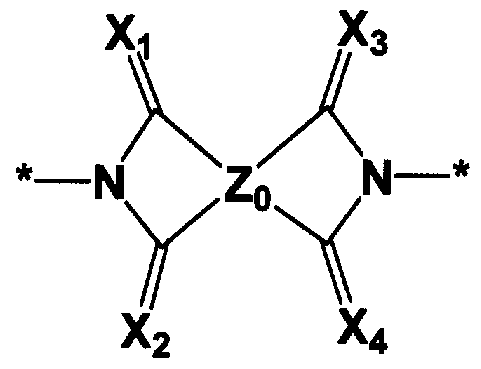


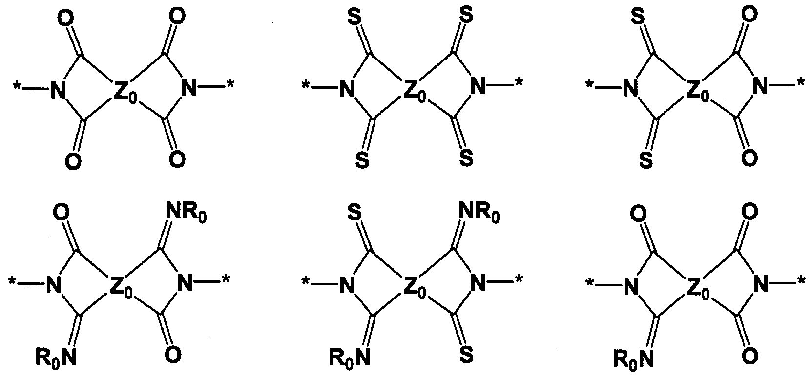

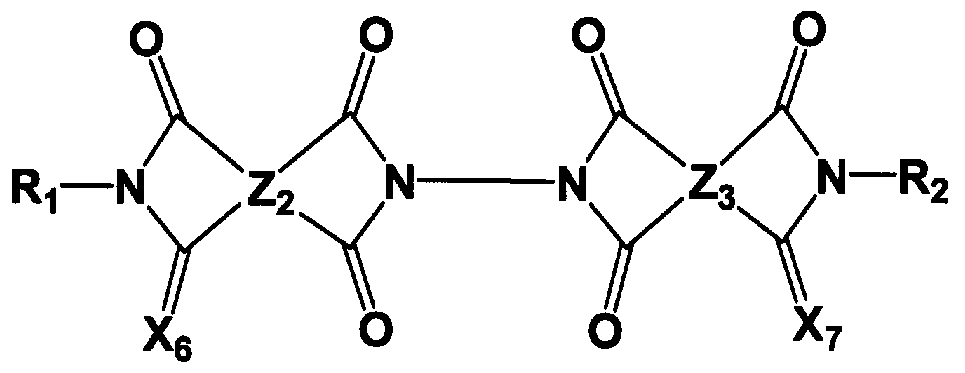
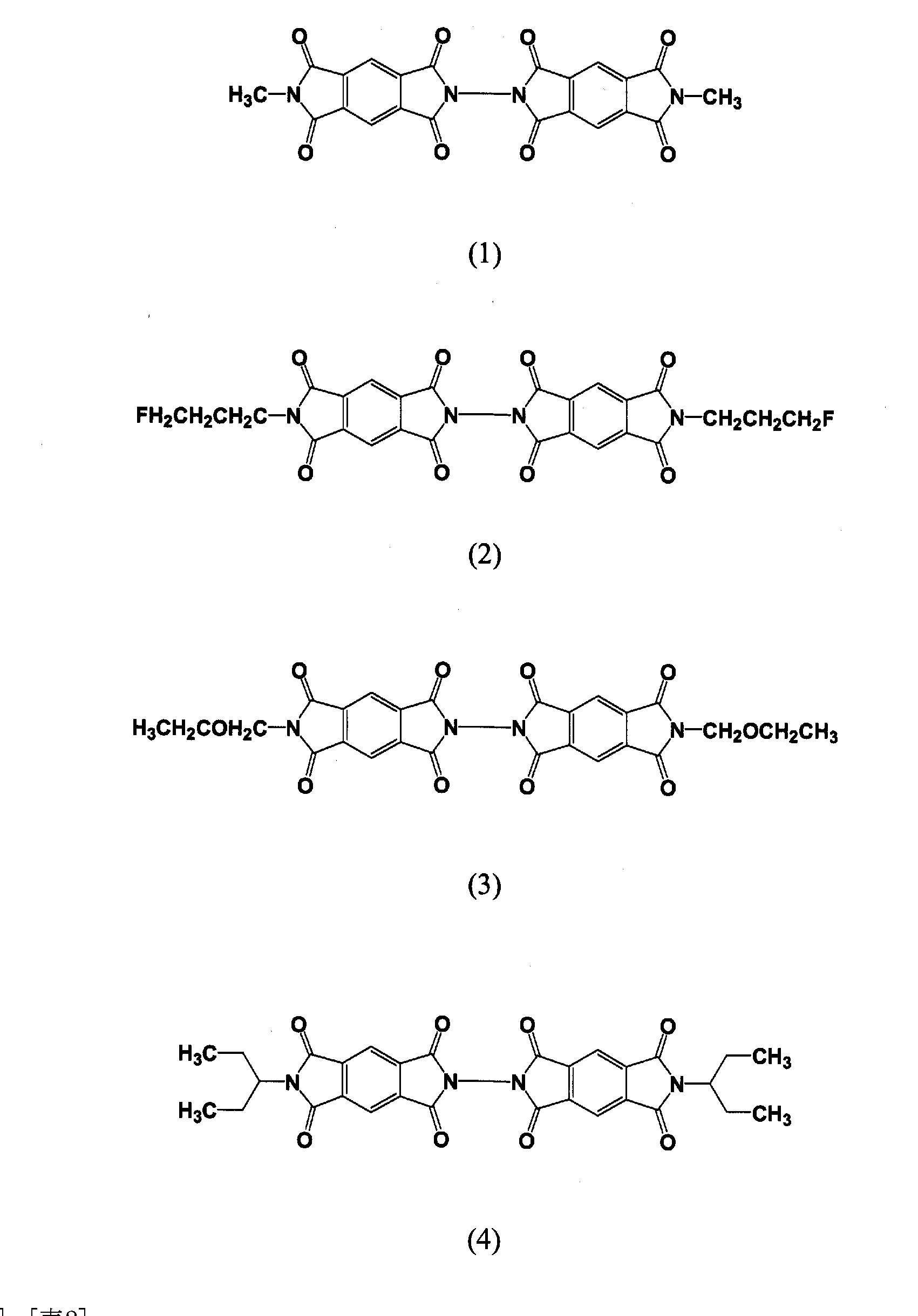


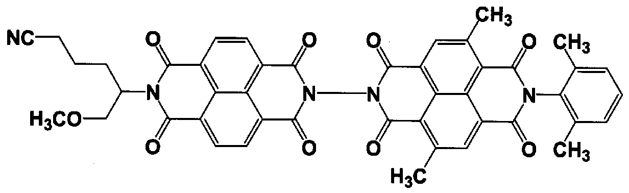


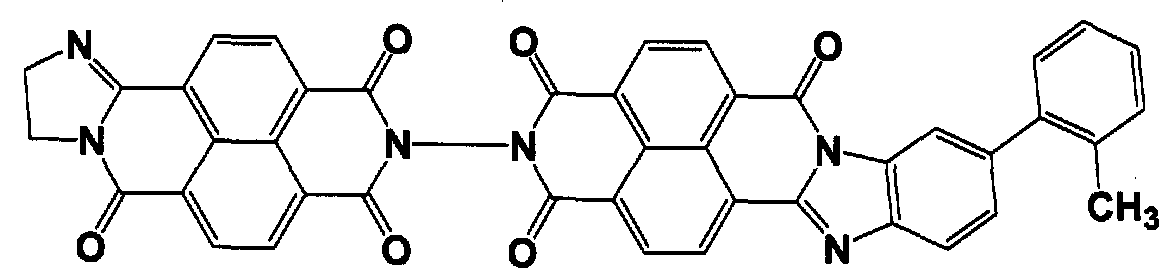


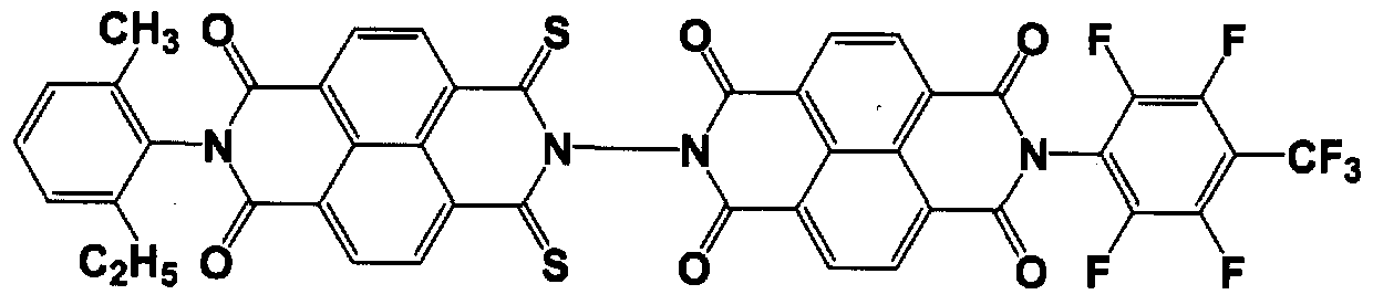


Claims


Priority Applications (4)
| Application Number | Priority Date | Filing Date | Title |
|---|---|---|---|
| CN200580010086.5A CN1938321B (en) | 2004-03-29 | 2005-03-29 | Novel compound and organic electronic device using such compound |
| EP05727671A EP1736476A4 (en) | 2004-03-29 | 2005-03-29 | Novel compound and organic electronic device using such compound |
| US10/594,156 US7763727B2 (en) | 2004-03-29 | 2005-03-29 | Compound and organic electronic device using the same |
| JP2006511588A JP4627528B2 (en) | 2004-03-29 | 2005-03-29 | Novel compound and organic electronic device using the compound |
Applications Claiming Priority (6)
| Application Number | Priority Date | Filing Date | Title |
|---|---|---|---|
| JP2004-094088 | 2004-03-29 | ||
| JP2004094088 | 2004-03-29 | ||
| JP2004277461 | 2004-09-24 | ||
| JP2004-277461 | 2004-09-24 | ||
| JP2004351088 | 2004-12-03 | ||
| JP2004-351088 | 2004-12-03 |
Publications (1)
| Publication Number | Publication Date |
|---|---|
| WO2005092901A1 true WO2005092901A1 (en) | 2005-10-06 |
Family
ID=35056132
Family Applications (1)
| Application Number | Title | Priority Date | Filing Date |
|---|---|---|---|
| PCT/JP2005/005979 WO2005092901A1 (en) | 2004-03-29 | 2005-03-29 | Novel compound and organic electronic device using such compound |
Country Status (6)
| Country | Link |
|---|---|
| US (1) | US7763727B2 (en) |
| EP (1) | EP1736476A4 (en) |
| JP (1) | JP4627528B2 (en) |
| KR (1) | KR100861434B1 (en) |
| CN (1) | CN1938321B (en) |
| WO (1) | WO2005092901A1 (en) |
Cited By (74)
| Publication number | Priority date | Publication date | Assignee | Title |
|---|---|---|---|---|
| JP2007094360A (en) * | 2005-09-02 | 2007-04-12 | Ricoh Co Ltd | Electrophotographic apparatus |
| JP2007108637A (en) * | 2005-09-13 | 2007-04-26 | Ricoh Co Ltd | Electrophotographic apparatus |
| JP2007108658A (en) * | 2005-09-16 | 2007-04-26 | Ricoh Co Ltd | Image forming apparatus and process cartridge for image forming apparatus |
| JP2007108646A (en) * | 2005-09-15 | 2007-04-26 | Ricoh Co Ltd | Electrophotographic apparatus |
| JP2007108667A (en) * | 2005-09-14 | 2007-04-26 | Ricoh Co Ltd | Process cartridge and image forming apparatus |
| JP2007108632A (en) * | 2005-09-14 | 2007-04-26 | Ricoh Co Ltd | Electrophotographic apparatus |
| JP2007108665A (en) * | 2005-09-15 | 2007-04-26 | Ricoh Co Ltd | Electrophotographic photoreceptor, image forming apparatus, full-color image forming apparatus, and process cartridge |
| JP2007108652A (en) * | 2005-09-16 | 2007-04-26 | Ricoh Co Ltd | Image forming apparatus and process cartridge |
| JP2007108671A (en) * | 2005-09-15 | 2007-04-26 | Ricoh Co Ltd | Electrophotographic photoreceptor, image forming apparatus, and process cartridge |
| JP2007108650A (en) * | 2005-09-15 | 2007-04-26 | Ricoh Co Ltd | Image forming apparatus, image forming method and process cartridge |
| JP2007108659A (en) * | 2005-09-15 | 2007-04-26 | Ricoh Co Ltd | Electrophotographic photoconductor and electrophotographic apparatus |
| JP2007108651A (en) * | 2005-09-16 | 2007-04-26 | Ricoh Co Ltd | Photoreceptor, image forming apparatus, and process cartridge |
| JP2007108633A (en) * | 2005-09-13 | 2007-04-26 | Ricoh Co Ltd | Electrophotographic apparatus |
| JP2007108645A (en) * | 2005-09-16 | 2007-04-26 | Ricoh Co Ltd | Image forming apparatus and process cartridge |
| JP2007108682A (en) * | 2005-09-15 | 2007-04-26 | Ricoh Co Ltd | Image forming apparatus |
| JP2007108670A (en) * | 2005-09-15 | 2007-04-26 | Ricoh Co Ltd | Electrophotographic photoconductor, image forming apparatus, full-color image forming apparatus and process cartridge |
| JP2007108649A (en) * | 2005-09-16 | 2007-04-26 | Ricoh Co Ltd | Process cartridge, image forming apparatus and image forming method |
| JP2007108644A (en) * | 2005-09-15 | 2007-04-26 | Ricoh Co Ltd | Image forming apparatus and process cartridge |
| JP2007108719A (en) * | 2005-09-15 | 2007-04-26 | Ricoh Co Ltd | Electrophotographic photoconductor, image forming apparatus, full-color image forming apparatus and process cartridge |
| JP2007108636A (en) * | 2005-09-15 | 2007-04-26 | Ricoh Co Ltd | Electrophotographic apparatus, electrophotographic image forming method and process cartridge |
| JP2007108647A (en) * | 2005-09-15 | 2007-04-26 | Ricoh Co Ltd | Electrophotographic apparatus |
| JP2007108643A (en) * | 2005-09-16 | 2007-04-26 | Ricoh Co Ltd | Image forming apparatus and process cartridge |
| JP2007187728A (en) * | 2006-01-11 | 2007-07-26 | Canon Inc | Electrophotographic photoreceptor, process cartridge and electrophotographic apparatus |
| JP2007219126A (en) * | 2006-02-16 | 2007-08-30 | Ricoh Co Ltd | Image forming apparatus |
| JP2007233116A (en) * | 2006-03-02 | 2007-09-13 | Ricoh Co Ltd | Electrophotographic photoreceptor, image forming apparatus, and process cartridge |
| JP2007264589A (en) * | 2005-09-15 | 2007-10-11 | Ricoh Co Ltd | Image forming method and image forming apparatus |
| EP1847882A1 (en) * | 2006-04-20 | 2007-10-24 | Ricoh Company, Ltd. | Electrophotographic photoconductor, image forming apparatus, and process cartridge |
| JP2007286536A (en) * | 2006-04-20 | 2007-11-01 | Ricoh Co Ltd | Electrophotographic photoreceptor, image forming apparatus and process cartridge |
| JP2007304365A (en) * | 2006-05-12 | 2007-11-22 | Ricoh Co Ltd | Image forming apparatus |
| JP2007322576A (en) * | 2006-05-31 | 2007-12-13 | Ricoh Co Ltd | Electrophotographic photoreceptor, image forming apparatus and process cartridge |
| JP2008033207A (en) * | 2005-09-15 | 2008-02-14 | Ricoh Co Ltd | Electrophotographic photoconductor, image forming apparatus, full-color image forming apparatus and process cartridge |
| JP2008052014A (en) * | 2006-08-24 | 2008-03-06 | Ricoh Co Ltd | Electrophotographic photoreceptor, image forming apparatus, and process cartridge |
| JP2008065115A (en) * | 2006-09-08 | 2008-03-21 | Ricoh Co Ltd | Image forming apparatus |
| WO2008051552A2 (en) * | 2006-10-25 | 2008-05-02 | Northwestern University | Organic semiconductor materials and methods of preparing and use thereof |
| JP2008122740A (en) * | 2006-11-14 | 2008-05-29 | Ricoh Co Ltd | Electrophotographic photoreceptor, image forming apparatus and process cartridge |
| JP2008122763A (en) * | 2006-11-14 | 2008-05-29 | Ricoh Co Ltd | Image forming apparatus |
| JP2008216713A (en) * | 2007-03-06 | 2008-09-18 | Ricoh Co Ltd | Image forming method and image forming apparatus |
| JP2008224785A (en) * | 2007-03-09 | 2008-09-25 | Ricoh Co Ltd | Image forming apparatus and process cartridge |
| JP2008281800A (en) * | 2007-05-11 | 2008-11-20 | Ricoh Co Ltd | Electrophotographic photoreceptor, and image forming apparatus and process cartridge using the same |
| JP2008281805A (en) * | 2007-05-11 | 2008-11-20 | Ricoh Co Ltd | Image forming apparatus and process cartridge for image forming apparatus |
| WO2009005669A3 (en) * | 2007-06-29 | 2009-03-12 | Eastman Kodak Co | Tetracarboxylic diimide semiconductor for thin film transistors |
| JP2009099941A (en) * | 2007-09-28 | 2009-05-07 | Fujifilm Corp | Radiation detector, method of manufacturing radiation detector, coating liquid and method of manufacturing organic polymer layer |
| JP2009292802A (en) * | 2007-09-10 | 2009-12-17 | Ricoh Co Ltd | Naphthalenetetracarboxylic acid diimide derivative and electrophotographic photoreceptor using the same |
| US7671202B2 (en) | 2004-01-26 | 2010-03-02 | Northwestern University | Perylene n-type semiconductors and related devices |
| US7747197B2 (en) * | 2005-09-13 | 2010-06-29 | Ricoh Company, Ltd. | Electrophotographic image forming apparatus and process cartridge |
| JP2010254608A (en) * | 2009-04-23 | 2010-11-11 | Idemitsu Kosan Co Ltd | Phthalimide compound, naphthalimide compound, naphthalic anhydride compound, electron transporting material including these compounds and organic thin film solar cell |
| JP2010537427A (en) * | 2007-08-23 | 2010-12-02 | エスアールアイ インターナショナル | Electroluminescent device using organic cathode |
| US7871747B2 (en) * | 2005-09-13 | 2011-01-18 | Ricoh Company, Ltd. | Electrophotographic photoconductor having charge blocking and moire preventing layers |
| US7893265B2 (en) | 2007-01-08 | 2011-02-22 | Polyera Corporation | Methods for preparing arene-BIS (dicarboximide)-based semiconducting materials and related intermediates for preparing same |
| US7902363B2 (en) | 2006-11-17 | 2011-03-08 | Polyera Corporation | Diimide-based semiconductor materials and methods of preparing and using the same |
| US8007972B2 (en) * | 2005-09-15 | 2011-08-30 | Ricoh Company, Ltd. | Electrophotographic photoconductor, and image forming apparatus, process cartridge and image forming method using the same |
| JP2011524862A (en) * | 2008-05-30 | 2011-09-08 | ビーエーエスエフ ソシエタス・ヨーロピア | Semiconductor material, method for producing the same and use thereof |
| US8022214B2 (en) | 2007-01-24 | 2011-09-20 | Polyera Corporation | Organic semiconductor materials and precursors thereof |
| JP2013032296A (en) * | 2011-08-01 | 2013-02-14 | Ricoh Co Ltd | Bisdiazapentadiene derivative and method for producing the same |
| JP2014224987A (en) * | 2013-04-25 | 2014-12-04 | キヤノン株式会社 | Electrophotographic photosensitive member, process cartridge, electrophotographic apparatus, and imide compound |
| US9266892B2 (en) | 2012-12-19 | 2016-02-23 | Incyte Holdings Corporation | Fused pyrazoles as FGFR inhibitors |
| US9388185B2 (en) | 2012-08-10 | 2016-07-12 | Incyte Holdings Corporation | Substituted pyrrolo[2,3-b]pyrazines as FGFR inhibitors |
| US9533984B2 (en) | 2013-04-19 | 2017-01-03 | Incyte Holdings Corporation | Bicyclic heterocycles as FGFR inhibitors |
| US9533954B2 (en) | 2010-12-22 | 2017-01-03 | Incyte Corporation | Substituted imidazopyridazines and benzimidazoles as inhibitors of FGFR3 |
| US9580423B2 (en) | 2015-02-20 | 2017-02-28 | Incyte Corporation | Bicyclic heterocycles as FGFR4 inhibitors |
| US9611267B2 (en) | 2012-06-13 | 2017-04-04 | Incyte Holdings Corporation | Substituted tricyclic compounds as FGFR inhibitors |
| US9708318B2 (en) | 2015-02-20 | 2017-07-18 | Incyte Corporation | Bicyclic heterocycles as FGFR4 inhibitors |
| US9890156B2 (en) | 2015-02-20 | 2018-02-13 | Incyte Corporation | Bicyclic heterocycles as FGFR4 inhibitors |
| US10611762B2 (en) | 2017-05-26 | 2020-04-07 | Incyte Corporation | Crystalline forms of a FGFR inhibitor and processes for preparing the same |
| US10851105B2 (en) | 2014-10-22 | 2020-12-01 | Incyte Corporation | Bicyclic heterocycles as FGFR4 inhibitors |
| US11174257B2 (en) | 2018-05-04 | 2021-11-16 | Incyte Corporation | Salts of an FGFR inhibitor |
| US11407750B2 (en) | 2019-12-04 | 2022-08-09 | Incyte Corporation | Derivatives of an FGFR inhibitor |
| US11466004B2 (en) | 2018-05-04 | 2022-10-11 | Incyte Corporation | Solid forms of an FGFR inhibitor and processes for preparing the same |
| US11566028B2 (en) | 2019-10-16 | 2023-01-31 | Incyte Corporation | Bicyclic heterocycles as FGFR inhibitors |
| US11591329B2 (en) | 2019-07-09 | 2023-02-28 | Incyte Corporation | Bicyclic heterocycles as FGFR inhibitors |
| US11607416B2 (en) | 2019-10-14 | 2023-03-21 | Incyte Corporation | Bicyclic heterocycles as FGFR inhibitors |
| US11628162B2 (en) | 2019-03-08 | 2023-04-18 | Incyte Corporation | Methods of treating cancer with an FGFR inhibitor |
| US11897891B2 (en) | 2019-12-04 | 2024-02-13 | Incyte Corporation | Tricyclic heterocycles as FGFR inhibitors |
| US11939331B2 (en) | 2021-06-09 | 2024-03-26 | Incyte Corporation | Tricyclic heterocycles as FGFR inhibitors |
Families Citing this family (33)
| Publication number | Priority date | Publication date | Assignee | Title |
|---|---|---|---|---|
| US20070018153A1 (en) * | 2005-07-20 | 2007-01-25 | Osram-Opto Semiconductors Gmbh | Thick light emitting polymers to enhance oled efficiency and lifetime |
| DE102005053995A1 (en) | 2005-11-10 | 2007-05-24 | Basf Ag | Use of rylene derivatives as photosensitizers in solar cells |
| KR101221761B1 (en) * | 2006-12-01 | 2013-01-11 | 삼성전자주식회사 | Producing method of high-performance organic thin film transistor using oxidation and selective reduction of organic semiconductor materials |
| JP5168478B2 (en) * | 2007-06-04 | 2013-03-21 | 株式会社リコー | Electrophotographic photosensitive member, electrophotographic method, electrophotographic apparatus, and process cartridge for electrophotographic apparatus |
| EP2000856B1 (en) * | 2007-06-04 | 2011-02-02 | Ricoh Company, Ltd. | Electrophotographic photoreceptor, image forming apparatus, and process cartridge |
| JP5436418B2 (en) * | 2007-07-10 | 2014-03-05 | ビーエーエスエフ ソシエタス・ヨーロピア | Mixtures that produce photoactive layers in organic solar cells and organic photodetectors |
| US7906724B2 (en) | 2007-07-31 | 2011-03-15 | Agency For Science, Technology And Research | N-type conjugated materials based on 2-vinyl-4,5-dicyanoimidazoles and their use in organic photovoltaics |
| US8380109B2 (en) * | 2008-01-11 | 2013-02-19 | Ricoh Company, Ltd. | Image forming apparatus and process cartridge |
| TWI478624B (en) * | 2008-03-27 | 2015-03-21 | Nippon Steel & Sumikin Chem Co | Organic electroluminescent elements |
| US20120211063A1 (en) * | 2009-03-17 | 2012-08-23 | Jong-Jan Lee | Back Contact Solar Cell with Organic Semiconductor Heterojunctions |
| CN101508893B (en) * | 2009-03-23 | 2012-10-03 | 安徽大学 | 1,4,5,8-naphthalenetetracarboxylic imide derivative bifluorescent material and method of preparing the same |
| KR101249686B1 (en) | 2009-07-16 | 2013-04-05 | 주식회사 엘지화학 | Polyimide and photoresist resin composition comprising therof |
| KR20120083294A (en) * | 2009-07-27 | 2012-07-25 | 더 리젠츠 오브 더 유니버시티 오브 미시간 | Bulk heterojunction organic photovoltaic cells made by glancing angle deposition |
| US8440828B2 (en) | 2009-12-29 | 2013-05-14 | Polyera Corporation | Organic semiconductors and devices incorporating same |
| WO2011127475A1 (en) * | 2010-04-09 | 2011-10-13 | The Arizona Board Of Regents On Behalf Of The University Of Arizona | Organic photovoltaic devices comprising solution- processed substituted metal-phthalocyanines and exhibiting near-ir photo-sensitivity |
| JP5479228B2 (en) * | 2010-05-28 | 2014-04-23 | 三洋電機株式会社 | Solar cell module |
| KR101117127B1 (en) * | 2010-08-06 | 2012-02-24 | 한국과학기술연구원 | Tandem solar cell using amorphous silicon solar cell and organic solar cell |
| WO2012106119A1 (en) * | 2011-02-03 | 2012-08-09 | Konarka Technologies, Inc. | Photovoltaic cells |
| JP2014517820A (en) | 2011-04-15 | 2014-07-24 | ジョージア テック リサーチ コーポレーション | Stannyl derivatives of naphthalene diimide and related compositions and methods |
| US20130263925A1 (en) * | 2012-04-05 | 2013-10-10 | Merck Patent Gmbh | Hole Carrier Layer For Organic Photovoltaic Device |
| US9276157B2 (en) * | 2012-08-31 | 2016-03-01 | First Solar, Inc. | Methods of treating a semiconductor layer |
| ES2471568B1 (en) * | 2012-11-22 | 2015-08-21 | Abengoa Solar New Technologies S.A. | Procedure for creating electrical contacts and contacts thus created |
| US20140174496A1 (en) * | 2012-12-21 | 2014-06-26 | Georgia Tech Research Corporation | Hybrid generator using thermoelectric generation and piezoelectric generation |
| US20140203259A1 (en) * | 2013-01-18 | 2014-07-24 | Universal Display Corporation | Host for organic light emitting devices |
| CN104078594A (en) * | 2013-03-27 | 2014-10-01 | 海洋王照明科技股份有限公司 | Organic light-emitting device and fabrication method thereof |
| CN104051671B (en) | 2014-06-16 | 2016-03-16 | 京东方科技集团股份有限公司 | A kind of OLED display and preparation method thereof |
| WO2016159244A1 (en) * | 2015-04-03 | 2016-10-06 | 京セラドキュメントソリューションズ株式会社 | Positively chargeable single-layer electrophotographic photosensitive body, process cartridge and image forming device |
| US9711350B2 (en) | 2015-06-03 | 2017-07-18 | Asm Ip Holding B.V. | Methods for semiconductor passivation by nitridation |
| CN105655480A (en) * | 2016-01-04 | 2016-06-08 | 京东方科技集团股份有限公司 | Piezoelectric film sensor, piezoelectric film sensor circuit and manufacturing method |
| US11778896B2 (en) | 2017-06-16 | 2023-10-03 | Ubiquitous Energy, Inc. | Visibly transparent, near-infrared-absorbing metal-complex photovoltaic devices |
| US11545635B2 (en) | 2017-06-16 | 2023-01-03 | Ubiquitous Energy, Inc. | Visibly transparent, near-infrared-absorbing boron-containing photovoltaic devices |
| US10903438B2 (en) * | 2017-06-16 | 2021-01-26 | Ubiquitous Energy, Inc. | Visibly transparent, ultraviolet-absorbing photovoltaic devices |
| CN112286016B (en) * | 2019-07-22 | 2023-08-25 | 广东乐普泰新材料科技有限公司 | Single-layer electropositive organic photosensitive drum and preparation method thereof |
Citations (10)
| Publication number | Priority date | Publication date | Assignee | Title |
|---|---|---|---|---|
| JPH05148812A (en) * | 1991-11-29 | 1993-06-15 | Nippon Samikon Kk | Precast concrete pavement slab for road heating |
| US5645965A (en) | 1996-08-08 | 1997-07-08 | Xerox Corporation | Symmetrical perylene dimers |
| JPH11124382A (en) | 1997-07-24 | 1999-05-11 | Ciba Specialty Chem Holding Inc | A novel carbonyl reagent that can derive carbonyl compound to fluorescent compound |
| JPH11212283A (en) * | 1998-01-26 | 1999-08-06 | Konica Corp | Electrophographic photoreceptor |
| US6051351A (en) | 1999-05-21 | 2000-04-18 | Xerox Corporation | Perylenes |
| JP2000214611A (en) * | 1999-01-25 | 2000-08-04 | Kyocera Mita Corp | Electrophotographic photoreceptor |
| JP2004093803A (en) * | 2002-08-30 | 2004-03-25 | Canon Inc | Electrophotographic photoreceptor, process cartridge and electrophotographic apparatus |
| JP2004093791A (en) * | 2002-08-30 | 2004-03-25 | Canon Inc | Naphthalene amidine imide compound, electrophotographic photoreceptor containing the compound, process cartridge and electrophotographic apparatus with the photoreceptor |
| JP2005126367A (en) * | 2003-10-23 | 2005-05-19 | Mitsui Chemicals Inc | Naphthalenecarboxylic acid derivative, electrophotographic photoreceptor using the compound, and electrophotographic device |
| JP2005154409A (en) * | 2003-07-16 | 2005-06-16 | Mitsui Chemicals Inc | New naphthalene carboxylic acid derivative, electrophotographic photoreceptor by using the same and electrophotographic device |
Family Cites Families (5)
| Publication number | Priority date | Publication date | Assignee | Title |
|---|---|---|---|---|
| JP2718048B2 (en) | 1988-02-15 | 1998-02-25 | 株式会社ブリヂストン | Charge transport agent for electrophotographic photosensitive member and electrophotographic photosensitive member |
| JP2922212B2 (en) | 1989-02-17 | 1999-07-19 | パイオニア株式会社 | EL device |
| JPH05142812A (en) | 1991-11-16 | 1993-06-11 | Kao Corp | Electrophotographic sensitive body |
| JP2001052204A (en) | 1999-08-10 | 2001-02-23 | Monorisu:Kk | Method for encoding and decoding object and device capable of utilizing the same method |
| JP4078113B2 (en) * | 2002-05-10 | 2008-04-23 | キヤノン株式会社 | Method for producing naphthalenetetracarboxylic acid diimide compound |
-
2005
- 2005-03-29 EP EP05727671A patent/EP1736476A4/en not_active Withdrawn
- 2005-03-29 US US10/594,156 patent/US7763727B2/en not_active Expired - Fee Related
- 2005-03-29 KR KR1020067021674A patent/KR100861434B1/en not_active IP Right Cessation
- 2005-03-29 JP JP2006511588A patent/JP4627528B2/en not_active Expired - Fee Related
- 2005-03-29 WO PCT/JP2005/005979 patent/WO2005092901A1/en active Application Filing
- 2005-03-29 CN CN200580010086.5A patent/CN1938321B/en not_active Expired - Fee Related
Patent Citations (13)
| Publication number | Priority date | Publication date | Assignee | Title |
|---|---|---|---|---|
| JPH05148812A (en) * | 1991-11-29 | 1993-06-15 | Nippon Samikon Kk | Precast concrete pavement slab for road heating |
| US5645965A (en) | 1996-08-08 | 1997-07-08 | Xerox Corporation | Symmetrical perylene dimers |
| JPH10133403A (en) | 1996-08-08 | 1998-05-22 | Xerox Corp | Symmetric perylene dimer |
| US6060601A (en) | 1997-07-24 | 2000-05-09 | Ciba Specialty Chemicals Corporation | Fluorescence-derivatisation of carbonyl compounds-novel carbonyl reagents |
| JPH11124382A (en) | 1997-07-24 | 1999-05-11 | Ciba Specialty Chem Holding Inc | A novel carbonyl reagent that can derive carbonyl compound to fluorescent compound |
| JPH11212283A (en) * | 1998-01-26 | 1999-08-06 | Konica Corp | Electrophographic photoreceptor |
| JP2000214611A (en) * | 1999-01-25 | 2000-08-04 | Kyocera Mita Corp | Electrophotographic photoreceptor |
| US6051351A (en) | 1999-05-21 | 2000-04-18 | Xerox Corporation | Perylenes |
| JP2001005204A (en) | 1999-05-21 | 2001-01-12 | Xerox Corp | Photoconductive image forming member |
| JP2004093803A (en) * | 2002-08-30 | 2004-03-25 | Canon Inc | Electrophotographic photoreceptor, process cartridge and electrophotographic apparatus |
| JP2004093791A (en) * | 2002-08-30 | 2004-03-25 | Canon Inc | Naphthalene amidine imide compound, electrophotographic photoreceptor containing the compound, process cartridge and electrophotographic apparatus with the photoreceptor |
| JP2005154409A (en) * | 2003-07-16 | 2005-06-16 | Mitsui Chemicals Inc | New naphthalene carboxylic acid derivative, electrophotographic photoreceptor by using the same and electrophotographic device |
| JP2005126367A (en) * | 2003-10-23 | 2005-05-19 | Mitsui Chemicals Inc | Naphthalenecarboxylic acid derivative, electrophotographic photoreceptor using the compound, and electrophotographic device |
Non-Patent Citations (20)
| Title |
|---|
| DEBRECZENY ET AL., J. AM. CHEM. SOC., vol. 118, 1996, pages 8174 - 8175 |
| DEBRECZENY M. ET AL: "Femtosecond Optical Control of Charge Shift within Electron Donor-Acceptor Arrays: An Approach to Molecular Swithches.", JOURNAL OF HTE AMERICAN CHEMICAL SOCIETY., vol. 118, no. 34, 28 August 1996 (1996-08-28), pages 8174 - 8175, XP002990120 * |
| DINE-HART ET AL., DIE MAKROMOLECULARE CHEMIE, vol. 153, 1972, pages 237 - 54 |
| DINE-HART R.A. ET AL: "Effect of structural variations on the thermooxidative stability of aromatic polymides.", MEKROMOLEKULARE CHEMIE., vol. 153, 14 March 1972 (1972-03-14), pages 237 - 54, XP002990124 * |
| GIAIMO ET AL., J. AM. CHEM. SOC., vol. 124, 2002, pages 8530 - 8531 |
| GIAIMO J. ET AL: "Excited-state symmetry breaking in cofacial and linear dimers of a green perylenediimide chlorophyll analogue leading to ultrafast charge separation.", JOURNAL OF THE EMERICAN CHEMICAL SOCIETY., vol. 124, no. 29, 24 July 2002 (2002-07-24), pages 8530 - 8531, XP002990118 * |
| HEINEN ET AL., J. PHYS. CHEM. A, vol. 106, 2002, pages 1933 - 1937 |
| HEINEN U. ET AL: "High Time Resolution Q-Band EPR Study of Sequential Electron Transfer in a Triad Oriented in a Liquid Crystal.", JOURNAL OF PHYSICAL CHEMISTRY A., vol. 106, no. 10, 14 March 2002 (2002-03-14), pages 1933 - 1937, XP002990122 * |
| LANGHALS H. ET AL: "Intense dyes through chromophore-chromophore interactions: bi- and trichromophoric perylene-3,4:9,10-bis(dicarboximide)s.", ANGEWANDTE CHEMIE, INTERNATIONAL EDITION., vol. 37, no. 7, 20 April 1998 (1998-04-20), pages 952 - 955, XP000931227 * |
| LUKAS A. ET AL: "Biomimetic electron transfer using low energy excited states: A green perylene-based analogue of chlorophylla.", JOURNAL OF PHYSICAL CHEMISTRY., vol. 106, no. 6, 14 February 2002 (2002-02-14), pages 1299 - 1306, XP002990117 * |
| LUKAS A. ET AL: "Femtosecond Optical Switching of Electron Transport Direction in Branched Donor-Acceptor Arrays.", JOURNAL OF PHYSICAL CHEMISTRY B., vol. 104, no. 5, 10 February 2000 (2000-02-10), pages 931 - 940, XP002990121 * |
| LUKAS ET AL., J. PHYS. CHEM. B, vol. 104, 2000, pages 931 - 940 |
| LUKAS ET AL., J. PHYS. CHEM. B, vol. 106, 2002, pages 1299 - 1306 |
| MILLER ET AL., CHEMICAL PHYSICS, vol. 275, 2002, pages 167 - 183 |
| MILLER S. ET AL: "Ultrafast electron transfer reactions initiated by excited CT states of push-pull perylenes.", CHEMICAL PHYSICS., vol. 275, no. 1-3, 1 January 2002 (2002-01-01), pages 167 - 183, XP002990119 * |
| MORI ET AL., J. PHYS. CHEM. A, vol. 106, 2002, pages 4453 - 4467 |
| MORI Y. ET AL: "Spin effects on decay dynamics of charge-separeted states generated by photoinduced electron transfer in zinc porphyrin-naphthalenediimide dyads.", JOURNAL OF PHYSICAL CHEMISTRY., vol. 106, no. 18, 9 May 2002 (2002-05-09), pages 4453 - 4467, XP002971037 * |
| OKAMOTO ET AL., CHEM. EUR. J., vol. 10, 2004, pages 474 - 483 |
| OKAMOTO K. ET AL: "Effects of metal ions on photoinduced electron transfer in zinc prophyrin-naphthalenediimide linked systems.", CHEMISTRY--A EUROPEAN JOURNAL., vol. 10, no. 2, 23 January 2004 (2004-01-23), pages 474 - 483, XP002990123 * |
| See also references of EP1736476A4 |
Cited By (123)
| Publication number | Priority date | Publication date | Assignee | Title |
|---|---|---|---|---|
| US7982039B2 (en) | 2004-01-26 | 2011-07-19 | Northwestern University | N-type semiconductors and related devices |
| US7671202B2 (en) | 2004-01-26 | 2010-03-02 | Northwestern University | Perylene n-type semiconductors and related devices |
| JP2007094360A (en) * | 2005-09-02 | 2007-04-12 | Ricoh Co Ltd | Electrophotographic apparatus |
| US7871747B2 (en) * | 2005-09-13 | 2011-01-18 | Ricoh Company, Ltd. | Electrophotographic photoconductor having charge blocking and moire preventing layers |
| US8227156B2 (en) | 2005-09-13 | 2012-07-24 | Ricoh Company, Ltd. | Electrophotographic photoconductor, image forming apparatus, image forming method, and process cartridge |
| JP4567614B2 (en) * | 2005-09-13 | 2010-10-20 | 株式会社リコー | Electrophotographic equipment |
| JP4567615B2 (en) * | 2005-09-13 | 2010-10-20 | 株式会社リコー | Electrophotographic equipment |
| US7747197B2 (en) * | 2005-09-13 | 2010-06-29 | Ricoh Company, Ltd. | Electrophotographic image forming apparatus and process cartridge |
| JP2007108637A (en) * | 2005-09-13 | 2007-04-26 | Ricoh Co Ltd | Electrophotographic apparatus |
| JP2007108633A (en) * | 2005-09-13 | 2007-04-26 | Ricoh Co Ltd | Electrophotographic apparatus |
| US8064795B2 (en) | 2005-09-13 | 2011-11-22 | Ricoh Company, Ltd. | Electrophotographic image forming apparatus and process cartridge |
| JP2007108667A (en) * | 2005-09-14 | 2007-04-26 | Ricoh Co Ltd | Process cartridge and image forming apparatus |
| JP2007108632A (en) * | 2005-09-14 | 2007-04-26 | Ricoh Co Ltd | Electrophotographic apparatus |
| JP4562092B2 (en) * | 2005-09-14 | 2010-10-13 | 株式会社リコー | Electrophotographic equipment |
| JP4726716B2 (en) * | 2005-09-14 | 2011-07-20 | 株式会社リコー | Process cartridge and image forming apparatus |
| JP2007108670A (en) * | 2005-09-15 | 2007-04-26 | Ricoh Co Ltd | Electrophotographic photoconductor, image forming apparatus, full-color image forming apparatus and process cartridge |
| JP2007108665A (en) * | 2005-09-15 | 2007-04-26 | Ricoh Co Ltd | Electrophotographic photoreceptor, image forming apparatus, full-color image forming apparatus, and process cartridge |
| JP2007108644A (en) * | 2005-09-15 | 2007-04-26 | Ricoh Co Ltd | Image forming apparatus and process cartridge |
| JP2007108719A (en) * | 2005-09-15 | 2007-04-26 | Ricoh Co Ltd | Electrophotographic photoconductor, image forming apparatus, full-color image forming apparatus and process cartridge |
| JP2007108636A (en) * | 2005-09-15 | 2007-04-26 | Ricoh Co Ltd | Electrophotographic apparatus, electrophotographic image forming method and process cartridge |
| JP2007108647A (en) * | 2005-09-15 | 2007-04-26 | Ricoh Co Ltd | Electrophotographic apparatus |
| JP4705518B2 (en) * | 2005-09-15 | 2011-06-22 | 株式会社リコー | Electrophotographic photosensitive member and electrophotographic apparatus |
| JP2007108646A (en) * | 2005-09-15 | 2007-04-26 | Ricoh Co Ltd | Electrophotographic apparatus |
| JP2007108671A (en) * | 2005-09-15 | 2007-04-26 | Ricoh Co Ltd | Electrophotographic photoreceptor, image forming apparatus, and process cartridge |
| JP2007108650A (en) * | 2005-09-15 | 2007-04-26 | Ricoh Co Ltd | Image forming apparatus, image forming method and process cartridge |
| JP2007264589A (en) * | 2005-09-15 | 2007-10-11 | Ricoh Co Ltd | Image forming method and image forming apparatus |
| JP2007108659A (en) * | 2005-09-15 | 2007-04-26 | Ricoh Co Ltd | Electrophotographic photoconductor and electrophotographic apparatus |
| JP4726715B2 (en) * | 2005-09-15 | 2011-07-20 | 株式会社リコー | Electrophotographic photosensitive member, image forming apparatus, full-color image forming apparatus, and process cartridge |
| JP4728919B2 (en) * | 2005-09-15 | 2011-07-20 | 株式会社リコー | Image forming method and image forming apparatus |
| JP4741440B2 (en) * | 2005-09-15 | 2011-08-03 | 株式会社リコー | Electrophotographic photosensitive member, image forming apparatus, and process cartridge |
| JP2008033207A (en) * | 2005-09-15 | 2008-02-14 | Ricoh Co Ltd | Electrophotographic photoconductor, image forming apparatus, full-color image forming apparatus and process cartridge |
| JP4741441B2 (en) * | 2005-09-15 | 2011-08-03 | 株式会社リコー | Electrophotographic photosensitive member, image forming apparatus, and process cartridge |
| US8007972B2 (en) * | 2005-09-15 | 2011-08-30 | Ricoh Company, Ltd. | Electrophotographic photoconductor, and image forming apparatus, process cartridge and image forming method using the same |
| JP2007108682A (en) * | 2005-09-15 | 2007-04-26 | Ricoh Co Ltd | Image forming apparatus |
| JP2007108658A (en) * | 2005-09-16 | 2007-04-26 | Ricoh Co Ltd | Image forming apparatus and process cartridge for image forming apparatus |
| JP2007108643A (en) * | 2005-09-16 | 2007-04-26 | Ricoh Co Ltd | Image forming apparatus and process cartridge |
| JP4719616B2 (en) * | 2005-09-16 | 2011-07-06 | 株式会社リコー | Image forming apparatus and process cartridge |
| JP2007108645A (en) * | 2005-09-16 | 2007-04-26 | Ricoh Co Ltd | Image forming apparatus and process cartridge |
| JP2007108649A (en) * | 2005-09-16 | 2007-04-26 | Ricoh Co Ltd | Process cartridge, image forming apparatus and image forming method |
| JP2007108652A (en) * | 2005-09-16 | 2007-04-26 | Ricoh Co Ltd | Image forming apparatus and process cartridge |
| JP2007108651A (en) * | 2005-09-16 | 2007-04-26 | Ricoh Co Ltd | Photoreceptor, image forming apparatus, and process cartridge |
| JP4709014B2 (en) * | 2006-01-11 | 2011-06-22 | キヤノン株式会社 | Electrophotographic photosensitive member, process cartridge, and electrophotographic apparatus |
| JP2007187728A (en) * | 2006-01-11 | 2007-07-26 | Canon Inc | Electrophotographic photoreceptor, process cartridge and electrophotographic apparatus |
| JP2007219126A (en) * | 2006-02-16 | 2007-08-30 | Ricoh Co Ltd | Image forming apparatus |
| JP4621151B2 (en) * | 2006-02-16 | 2011-01-26 | 株式会社リコー | Image forming apparatus |
| JP2007233116A (en) * | 2006-03-02 | 2007-09-13 | Ricoh Co Ltd | Electrophotographic photoreceptor, image forming apparatus, and process cartridge |
| JP4607034B2 (en) * | 2006-03-02 | 2011-01-05 | 株式会社リコー | Electrophotographic photosensitive member, image forming apparatus, and process cartridge |
| EP1847882A1 (en) * | 2006-04-20 | 2007-10-24 | Ricoh Company, Ltd. | Electrophotographic photoconductor, image forming apparatus, and process cartridge |
| JP2007286536A (en) * | 2006-04-20 | 2007-11-01 | Ricoh Co Ltd | Electrophotographic photoreceptor, image forming apparatus and process cartridge |
| JP4722758B2 (en) * | 2006-04-20 | 2011-07-13 | 株式会社リコー | Electrophotographic photosensitive member, image forming apparatus, and process cartridge |
| US8192905B2 (en) | 2006-04-20 | 2012-06-05 | Ricoh Company, Ltd. | Electrophotographic photoconductor, image forming apparatus, and process cartridge |
| US8059990B2 (en) * | 2006-05-12 | 2011-11-15 | Ricoh Company, Ltd. | Image forming apparatus |
| JP2007304365A (en) * | 2006-05-12 | 2007-11-22 | Ricoh Co Ltd | Image forming apparatus |
| JP4668121B2 (en) * | 2006-05-12 | 2011-04-13 | 株式会社リコー | Image forming apparatus |
| JP4719085B2 (en) * | 2006-05-31 | 2011-07-06 | 株式会社リコー | Electrophotographic photosensitive member, image forming apparatus, process cartridge |
| JP2007322576A (en) * | 2006-05-31 | 2007-12-13 | Ricoh Co Ltd | Electrophotographic photoreceptor, image forming apparatus and process cartridge |
| JP4731426B2 (en) * | 2006-08-24 | 2011-07-27 | 株式会社リコー | Electrophotographic photosensitive member, image forming apparatus, and process cartridge |
| JP2008052014A (en) * | 2006-08-24 | 2008-03-06 | Ricoh Co Ltd | Electrophotographic photoreceptor, image forming apparatus, and process cartridge |
| JP4641991B2 (en) * | 2006-09-08 | 2011-03-02 | 株式会社リコー | Image forming apparatus |
| JP2008065115A (en) * | 2006-09-08 | 2008-03-21 | Ricoh Co Ltd | Image forming apparatus |
| US7947837B2 (en) | 2006-10-25 | 2011-05-24 | Polyera Corporation | Organic semiconductor materials and methods of preparing and use thereof |
| WO2008051552A3 (en) * | 2006-10-25 | 2009-03-19 | Univ Northwestern | Organic semiconductor materials and methods of preparing and use thereof |
| WO2008051552A2 (en) * | 2006-10-25 | 2008-05-02 | Northwestern University | Organic semiconductor materials and methods of preparing and use thereof |
| JP2008122740A (en) * | 2006-11-14 | 2008-05-29 | Ricoh Co Ltd | Electrophotographic photoreceptor, image forming apparatus and process cartridge |
| US7919220B2 (en) | 2006-11-14 | 2011-04-05 | Ricoh Company, Ltd. | Electrophotographic photoreceptor, image forming apparatus and process cartridge |
| JP2008122763A (en) * | 2006-11-14 | 2008-05-29 | Ricoh Co Ltd | Image forming apparatus |
| US7902363B2 (en) | 2006-11-17 | 2011-03-08 | Polyera Corporation | Diimide-based semiconductor materials and methods of preparing and using the same |
| US7893265B2 (en) | 2007-01-08 | 2011-02-22 | Polyera Corporation | Methods for preparing arene-BIS (dicarboximide)-based semiconducting materials and related intermediates for preparing same |
| US8022214B2 (en) | 2007-01-24 | 2011-09-20 | Polyera Corporation | Organic semiconductor materials and precursors thereof |
| US8252499B2 (en) | 2007-03-06 | 2012-08-28 | Ricoh Company, Ltd. | Image forming method and image forming apparatus |
| JP2008216713A (en) * | 2007-03-06 | 2008-09-18 | Ricoh Co Ltd | Image forming method and image forming apparatus |
| JP2008224785A (en) * | 2007-03-09 | 2008-09-25 | Ricoh Co Ltd | Image forming apparatus and process cartridge |
| JP2008281805A (en) * | 2007-05-11 | 2008-11-20 | Ricoh Co Ltd | Image forming apparatus and process cartridge for image forming apparatus |
| JP2008281800A (en) * | 2007-05-11 | 2008-11-20 | Ricoh Co Ltd | Electrophotographic photoreceptor, and image forming apparatus and process cartridge using the same |
| US7858970B2 (en) | 2007-06-29 | 2010-12-28 | Eastman Kodak Company | Heterocycloalkyl-substituted naphthalene-based tetracarboxylic diimide compounds as N-type semiconductor materials for thin film transistors |
| WO2009005669A3 (en) * | 2007-06-29 | 2009-03-12 | Eastman Kodak Co | Tetracarboxylic diimide semiconductor for thin film transistors |
| JP2010534403A (en) * | 2007-06-29 | 2010-11-04 | イーストマン コダック カンパニー | Tetracarboxylic acid diimide semiconductors for thin film transistors |
| JP2010537427A (en) * | 2007-08-23 | 2010-12-02 | エスアールアイ インターナショナル | Electroluminescent device using organic cathode |
| JP2009292802A (en) * | 2007-09-10 | 2009-12-17 | Ricoh Co Ltd | Naphthalenetetracarboxylic acid diimide derivative and electrophotographic photoreceptor using the same |
| JP2009099941A (en) * | 2007-09-28 | 2009-05-07 | Fujifilm Corp | Radiation detector, method of manufacturing radiation detector, coating liquid and method of manufacturing organic polymer layer |
| JP2011524862A (en) * | 2008-05-30 | 2011-09-08 | ビーエーエスエフ ソシエタス・ヨーロピア | Semiconductor material, method for producing the same and use thereof |
| JP2010254608A (en) * | 2009-04-23 | 2010-11-11 | Idemitsu Kosan Co Ltd | Phthalimide compound, naphthalimide compound, naphthalic anhydride compound, electron transporting material including these compounds and organic thin film solar cell |
| US10213427B2 (en) | 2010-12-22 | 2019-02-26 | Incyte Corporation | Substituted imidazopyridazines and benzimidazoles as inhibitors of FGFR3 |
| US10813930B2 (en) | 2010-12-22 | 2020-10-27 | Incyte Corporation | Substituted imidazopyridazines and benzimidazoles as inhibitors of FGFR3 |
| US9533954B2 (en) | 2010-12-22 | 2017-01-03 | Incyte Corporation | Substituted imidazopyridazines and benzimidazoles as inhibitors of FGFR3 |
| JP2013032296A (en) * | 2011-08-01 | 2013-02-14 | Ricoh Co Ltd | Bisdiazapentadiene derivative and method for producing the same |
| US10131667B2 (en) | 2012-06-13 | 2018-11-20 | Incyte Corporation | Substituted tricyclic compounds as FGFR inhibitors |
| US11840534B2 (en) | 2012-06-13 | 2023-12-12 | Incyte Corporation | Substituted tricyclic compounds as FGFR inhibitors |
| US9611267B2 (en) | 2012-06-13 | 2017-04-04 | Incyte Holdings Corporation | Substituted tricyclic compounds as FGFR inhibitors |
| US11053246B2 (en) | 2012-06-13 | 2021-07-06 | Incyte Corporation | Substituted tricyclic compounds as FGFR inhibitors |
| US9388185B2 (en) | 2012-08-10 | 2016-07-12 | Incyte Holdings Corporation | Substituted pyrrolo[2,3-b]pyrazines as FGFR inhibitors |
| US9745311B2 (en) | 2012-08-10 | 2017-08-29 | Incyte Corporation | Substituted pyrrolo[2,3-b]pyrazines as FGFR inhibitors |
| US9266892B2 (en) | 2012-12-19 | 2016-02-23 | Incyte Holdings Corporation | Fused pyrazoles as FGFR inhibitors |
| US11530214B2 (en) | 2013-04-19 | 2022-12-20 | Incyte Holdings Corporation | Bicyclic heterocycles as FGFR inhibitors |
| US10450313B2 (en) | 2013-04-19 | 2019-10-22 | Incyte Holdings Corporation | Bicyclic heterocycles as FGFR inhibitors |
| US10040790B2 (en) | 2013-04-19 | 2018-08-07 | Incyte Holdings Corporation | Bicyclic heterocycles as FGFR inhibitors |
| US10947230B2 (en) | 2013-04-19 | 2021-03-16 | Incyte Corporation | Bicyclic heterocycles as FGFR inhibitors |
| US9533984B2 (en) | 2013-04-19 | 2017-01-03 | Incyte Holdings Corporation | Bicyclic heterocycles as FGFR inhibitors |
| JP2014224987A (en) * | 2013-04-25 | 2014-12-04 | キヤノン株式会社 | Electrophotographic photosensitive member, process cartridge, electrophotographic apparatus, and imide compound |
| US10851105B2 (en) | 2014-10-22 | 2020-12-01 | Incyte Corporation | Bicyclic heterocycles as FGFR4 inhibitors |
| US9890156B2 (en) | 2015-02-20 | 2018-02-13 | Incyte Corporation | Bicyclic heterocycles as FGFR4 inhibitors |
| US9708318B2 (en) | 2015-02-20 | 2017-07-18 | Incyte Corporation | Bicyclic heterocycles as FGFR4 inhibitors |
| US10632126B2 (en) | 2015-02-20 | 2020-04-28 | Incyte Corporation | Bicyclic heterocycles as FGFR4 inhibitors |
| US10738048B2 (en) | 2015-02-20 | 2020-08-11 | Incyte Corporation | Bicyclic heterocycles as FGFR4 inhibitors |
| US10214528B2 (en) | 2015-02-20 | 2019-02-26 | Incyte Corporation | Bicyclic heterocycles as FGFR4 inhibitors |
| US10016438B2 (en) | 2015-02-20 | 2018-07-10 | Incyte Corporation | Bicyclic heterocycles as FGFR4 inhibitors |
| US11667635B2 (en) | 2015-02-20 | 2023-06-06 | Incyte Corporation | Bicyclic heterocycles as FGFR4 inhibitors |
| US11014923B2 (en) | 2015-02-20 | 2021-05-25 | Incyte Corporation | Bicyclic heterocycles as FGFR4 inhibitors |
| US10251892B2 (en) | 2015-02-20 | 2019-04-09 | Incyte Corporation | Bicyclic heterocycles as FGFR4 inhibitors |
| US11173162B2 (en) | 2015-02-20 | 2021-11-16 | Incyte Corporation | Bicyclic heterocycles as FGFR4 inhibitors |
| US9801889B2 (en) | 2015-02-20 | 2017-10-31 | Incyte Corporation | Bicyclic heterocycles as FGFR4 inhibitors |
| US9580423B2 (en) | 2015-02-20 | 2017-02-28 | Incyte Corporation | Bicyclic heterocycles as FGFR4 inhibitors |
| US10611762B2 (en) | 2017-05-26 | 2020-04-07 | Incyte Corporation | Crystalline forms of a FGFR inhibitor and processes for preparing the same |
| US11472801B2 (en) | 2017-05-26 | 2022-10-18 | Incyte Corporation | Crystalline forms of a FGFR inhibitor and processes for preparing the same |
| US11174257B2 (en) | 2018-05-04 | 2021-11-16 | Incyte Corporation | Salts of an FGFR inhibitor |
| US11466004B2 (en) | 2018-05-04 | 2022-10-11 | Incyte Corporation | Solid forms of an FGFR inhibitor and processes for preparing the same |
| US11628162B2 (en) | 2019-03-08 | 2023-04-18 | Incyte Corporation | Methods of treating cancer with an FGFR inhibitor |
| US11591329B2 (en) | 2019-07-09 | 2023-02-28 | Incyte Corporation | Bicyclic heterocycles as FGFR inhibitors |
| US11607416B2 (en) | 2019-10-14 | 2023-03-21 | Incyte Corporation | Bicyclic heterocycles as FGFR inhibitors |
| US11566028B2 (en) | 2019-10-16 | 2023-01-31 | Incyte Corporation | Bicyclic heterocycles as FGFR inhibitors |
| US11407750B2 (en) | 2019-12-04 | 2022-08-09 | Incyte Corporation | Derivatives of an FGFR inhibitor |
| US11897891B2 (en) | 2019-12-04 | 2024-02-13 | Incyte Corporation | Tricyclic heterocycles as FGFR inhibitors |
| US11939331B2 (en) | 2021-06-09 | 2024-03-26 | Incyte Corporation | Tricyclic heterocycles as FGFR inhibitors |
Also Published As
| Publication number | Publication date |
|---|---|
| CN1938321A (en) | 2007-03-28 |
| JPWO2005092901A1 (en) | 2008-02-14 |
| EP1736476A1 (en) | 2006-12-27 |
| KR20060134167A (en) | 2006-12-27 |
| US20070219375A1 (en) | 2007-09-20 |
| EP1736476A4 (en) | 2010-04-07 |
| CN1938321B (en) | 2010-05-05 |
| US7763727B2 (en) | 2010-07-27 |
| KR100861434B1 (en) | 2008-10-02 |
| JP4627528B2 (en) | 2011-02-09 |
Similar Documents
| Publication | Publication Date | Title |
|---|---|---|
| JP4627528B2 (en) | Novel compound and organic electronic device using the compound | |
| JP5513386B2 (en) | Indenopyrene compound, organic thin film solar cell material and organic thin film solar cell using the same | |
| EP1763087B1 (en) | Photoelectric conversion devices | |
| JP5801306B2 (en) | Visible / NIR photodetector | |
| JP5452888B2 (en) | Organic thin film solar cell | |
| JP6907187B2 (en) | Organic compounds, near-infrared absorbing dyes, photoelectric conversion elements and their optical sensors, image sensors | |
| JP2010073987A (en) | Material for organic thin-film solar cell | |
| JP2010232410A (en) | Organic photoelectric conversion element | |
| JP5363164B2 (en) | Benzofluoranthene compound and organic thin film solar cell using the same | |
| WO2013031468A1 (en) | Heterocyclic compound and use thereof | |
| JP5498674B2 (en) | Organic thin film solar cell material and organic thin film solar cell using the same | |
| US20120298203A1 (en) | Dibenzofluoranthene compound and organic thin-film solar cell using same | |
| EP2599768A1 (en) | Indenoperylene compound, material for organic thin-film photovotaic cell containing indenoperylene derivative, and organic thin-film photovotaic cell using same | |
| JP5525895B2 (en) | Organic thin film solar cell material and organic thin film solar cell using the same | |
| JP5283980B2 (en) | Organic thin film solar cell material and organic thin film solar cell using the same | |
| US20170263870A1 (en) | 2,2'-bibenzo[d]imidazolidene compound having condensed rings at the 1-, 1'-, 3- and 3'-positions, and organic light-emitting element, display device, image information processing apparatus, lighting device, image forming apparatus and exposure unit, each containing the same | |
| JP5658937B2 (en) | Indenoperylene compound and organic thin film solar cell using the same | |
| JP2021015963A (en) | Photoelectric conversion element material and uses thereof | |
| JP2017132697A (en) | Organic compound and application thereof | |
| JP2013168470A (en) | Organic thin film solar cell material including dipyrrin compound and organic thin film solar cell manufactured using the same |
Legal Events
| Date | Code | Title | Description |
|---|---|---|---|
| AK | Designated states |
Kind code of ref document: A1 Designated state(s): AE AG AL AM AT AU AZ BA BB BG BR BW BY BZ CA CH CN CO CR CU CZ DE DK DM DZ EC EE EG ES FI GB GD GE GH GM HR HU ID IL IN IS JP KE KG KP KR KZ LC LK LR LS LT LU LV MA MD MG MK MN MW MX MZ NA NI NO NZ OM PG PH PL PT RO RU SC SD SE SG SK SL SM SY TJ TM TN TR TT TZ UA UG US UZ VC VN YU ZA ZM ZW |
|
| AL | Designated countries for regional patents |
Kind code of ref document: A1 Designated state(s): BW GH GM KE LS MW MZ NA SD SL SZ TZ UG ZM ZW AM AZ BY KG KZ MD RU TJ TM AT BE BG CH CY CZ DE DK EE ES FI FR GB GR HU IE IS IT LT LU MC NL PL PT RO SE SI SK TR BF BJ CF CG CI CM GA GN GQ GW ML MR NE SN TD TG |
|
| 121 | Ep: the epo has been informed by wipo that ep was designated in this application | ||
| WWE | Wipo information: entry into national phase |
Ref document number: 2006511588 Country of ref document: JP |
|
| WWE | Wipo information: entry into national phase |
Ref document number: 10594156 Country of ref document: US Ref document number: 2007219375 Country of ref document: US |
|
| WWE | Wipo information: entry into national phase |
Ref document number: 200580010086.5 Country of ref document: CN |
|
| NENP | Non-entry into the national phase |
Ref country code: DE |
|
| WWW | Wipo information: withdrawn in national office |
Ref document number: DE |
|
| REEP | Request for entry into the european phase |
Ref document number: 2005727671 Country of ref document: EP |
|
| WWE | Wipo information: entry into national phase |
Ref document number: 2005727671 Country of ref document: EP |
|
| WWE | Wipo information: entry into national phase |
Ref document number: 1020067021674 Country of ref document: KR |
|
| WWP | Wipo information: published in national office |
Ref document number: 2005727671 Country of ref document: EP Ref document number: 1020067021674 Country of ref document: KR |
|
| WWP | Wipo information: published in national office |
Ref document number: 10594156 Country of ref document: US |