WO1985002314A2 - Semiconductor memory - Google Patents
Semiconductor memory Download PDFInfo
- Publication number
- WO1985002314A2 WO1985002314A2 PCT/US1984/001839 US8401839W WO8502314A2 WO 1985002314 A2 WO1985002314 A2 WO 1985002314A2 US 8401839 W US8401839 W US 8401839W WO 8502314 A2 WO8502314 A2 WO 8502314A2
- Authority
- WO
- WIPO (PCT)
- Prior art keywords
- sense amplifiers
- column
- memory
- accordance
- transistors
- Prior art date
Links
Classifications
-
- G—PHYSICS
- G11—INFORMATION STORAGE
- G11C—STATIC STORES
- G11C7/00—Arrangements for writing information into, or reading information out from, a digital store
- G11C7/06—Sense amplifiers; Associated circuits, e.g. timing or triggering circuits
- G11C7/065—Differential amplifiers of latching type
Abstract
Inclusion of two or more sense amplifiers in a column of a solid state memory. In one embodiment, and additional sense amplifier (100) is provided on each column of a dynamic access memory (RAM). In other embodiment, a static memory has two or more sense amplifiers (S311, S321) located along a column. The sense amplifiers may be activated by the same column access strobe (CAS) pulse may be activated sequentially by separate strobe pulses (T1, T2). Other implementations of the present technique in ROMs, EPROMS, etc. are possible. The additional sense amplifiers provide improved signal transfer speed.
Description
SEMICONDUCTOR MEMORY
Background of the Invention
1. Field of the Invention The present invention relates to semiconductor memories, and particularly to the sense amplifier arrangements used in such memories.
2. Description of the Prior Art Semiconductor memories are frequently arranged in rectangular arrays of memory cells, wherein an individual cell is located at an intersection of perpendicular conductors. These conductors are typically referred to as "rows" and "columns" and access for reading information out of a given memory cell is accomplished by electrically selecting its row and column. Various memory cell types are known in the art, including dynamic RAMs, static RAMs, read only memories (ROMs), electrically programmable read only memories (EPROMs), etc. These various types differ mainly by how information is read into a cell, and how it is stored in the cell. However, regardless of the cell type, the information is typically read out onto at least one of two column conductors, referred to as a "bit line". During the read out operation, the memory cell induces a change in the relative voltage levels between the two column conductors to represent a logical "1" or "0". In the case of a dynamic RAM, one of the column conductors, referred to as the reference line, is placed at a reference voltage level during a read operation. In the case of a static RAM, one or both column conductors change voltage levels during a read operation. However, the voltage difference between the two conductors may be small, especially in the case of a one-transistor dynamic cell. Ire a multiple-transistor static cell, the speed at which a useful voltage difference is achieved is limited by memory cell size. Thus, for reasons including the necessity to sense small signals in a short time period, a sense amplifier is used.
In a typical sense amplifier arrangement, a bistable sensing amplifier is employed for sensing the voltage difference between the potential on the two conductors of the bit line. Each column conductor may also be referred to as half of the bit line. In the case of a dynamic RAM. this difference results from a sharing of the charge read from a reference cell onto one half of the bit line and from an accessed storage cell on the other half of the bit line. To refresh the electrical signals read out of the memory cells, switchable circuitry is included which is responsive to a timing signal generated after the sense amplifier has latched into a stable state.
One particular prior art dynamic RAM arrangement, disclosed in U S. Patent 4,069,475 issued to C. E. Boettcher on January 17, 1978, eliminates the need for separate restore timing signals by deriving such signals from a bistable sensing amplifier when the bistable sensing amplifier has switched sufficiently to exceed the turn-on threshold of the corresponding restore bypass switch. Such an arrangement also permits a reduction in the power dissipation of the sense amplifier.
An alternative arrangement is disclosed in U S. Patent 4,286,178 issued to G. R. Mohan Rao et al on August 25, 1981 Like the above-described Boettcher arrangement, the Rao et al sense amplifier circuit employs a bistable sense amplifier circuit at the center of each column. However, instead of a single pair of crosscoupled driver transistors forming the bistable circuit, dual parallel pairs are used in the Rao et al arrangement. One pair used in the initial sensing has a long channel length so that the pair may be more readily matched, while the other pair, used later in the cycle for driving the zero-going side of the column line to ground, has a shorter channel to enhance speed. In the case of static RAM, the difference in voltage between the two column conductors is due to the state of a bistable circuit as the memory cell. Typically,
two or four transistor cross-coupled circuits are utilized as the bistable memory cell circuit. The bistable circuit is typically connected to the column conductors through two access transistors, one for each conductor. These access transistors are activated by the corresponding row conductor typically referred to as the "word line". Thus, upon activating a given word line, the state of the memory cell in a selected bit line can be determined. However in contrast to dynamic RAMs, static RAMs in the prior art have shared sense amplifiers among several bit lines. For example, an 8Kx8 static memory typically includes only eight sense amplifiers that are multiplexed among 256 columns; see "An 8Kx8 Bit Static MOS RAM Fabricated by n- Mos/n-Well CMOS Technology", T. Ohzone et al, IEEE Journal of Solid-State Circuits , Vol. SC-15, No. 5, pp. 854-861 (1980).
As memory devices require higher packing density, higher speed and lower power dissipation the sense amplifiers become more critical. Some prior circuits exhibit high power dissipation and overly long charging and discharging times for the bit lines, while others require high instantaneous current and critical clock timing. Further, as the number of bits increases, the cell size decreases. In the case of a dynamic RAM the magnitude of the storage capacitor in each cell, of necessity, decreases, and the capacitance of the bit lines increase due to the increase in the number of cells on a bit line In the case of a static RAM, the size of the memory cell transistors decreases relative to the capacitance of the bit lines as the memory size increases These factors reduce the magnitude of the data signal which exists on a bit line, and the speed with which it can be sensed. Similar considerations apply to ROMs, EPROMs, and other memory devices. Thus, it would be desirable to provide an improved sense amplifier arrangement for memory configurations utilizing row and column conductors for
memory cell access with improved signal transfer speed, without unduly increasing the power dissipation. Summary of the Invention
The present invention relates to a semiconductor memory wherein two or more sense amplifiers are coupled directly to a given column of memory cells. At least some of the sense amplifiers are separated from one another by along the column by at least one memory cell. The sense amplifiers can be activated simultaneously, or activated sequentially, when a read or write operation is desired. The thresholds of the amplifiers can be the same, or may differ. In one embodiment, two or more sense amplifiers are spaced along a column of static memory cells. Brief Description of the Drawings FIG. 1 illustrates an exemplary column of a random access memory device formed in accordance with the present invention, and
FIG. 2 illustrates a timing diagram depicting various input and output signals related to the operation of the present invention.
FIG. 3 illustrates an exemplary memory device wherein a column decoder provides for simultaneous activation of the sense amplifiers associated with an accessed column. FIG. 4 illustrates an exemplary memory device wherein a sense amplifier strobe provides for sequential activation of sense amplifiers in columns that are accessed simultaneously.
FIG. 5 illustrates a portion of an exemplary column in a static memory device of the present invention. FIG. 6 illustrates a typical timing diagram for the circuitry shown in FIG. 5 Detailed Description
The present invention relates to a memory device having memory cells arranged in rows and columns, wherein at least two sense amplifiers are coupled directly to each column conductor pair and spaced along the column. As used
herein, the term "coupled directly to each column conductor pair" implies that the sense amplifiers are not multiplexed or otherwise shared among the column conductor pairs. However, it does not preclude the use of gated interrupt transistor to temporarily disconnect a sense amplifier from its respective column conductors during a portion of the memory cycle.
In many large dynamic RAM arrangements, for example, a 256K dynamic RAM, a folded-bit architecture may be employed to increase the density of the memory arrangement without increasing its physical size A pair of columns, Cn and of a folded-bit line
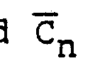 arrangement which illustrate the arrangement of the present invention are shown in FIG. 1. Data is stored in various ones of the memory cells included therein by activating the appropriate Rn line related thereto, and is accessed via I/O lines, denoted DQ and
 Q in FIG. 1.
For illustrative purposes, all transistors illustrated in FIG. 1 are assumed to be n-channel MOS transistors. An MOS transistor will be described as enabled if the potential of the gate is of sufficient amplitude and polarity with respect to the source to allow conduction between the source and the drain of the MOS transistor. Conversely, a disabled MOS transistor is one in which the potential of the gate is insufficient or of the wrong polarity to allow conduction between the source and drain.
Referring now to FIG. 1, an exemplary bit line is illustrated which includes a first sense amplifier 10 disposed at the end of the bit line which is "folded", and a second sense amplifier 100 disposed opposite thereof, near the DQ I/O line. As shown, first sense amplifier 10 includes transistors 12, 14, 16 and 18 Connected to one side of first sense amplifier 10 at a first outer terminal 20 is the source input of a column interrupt transistor 22. Similarly, the source input of a column interrupt transistor 26 is connected to first sense amplifier 10 at a second outer terminal 24. The gate
inputs of column interrupt transistors 22 and 26 are both coupled to a CCIB source (not shown) which, depending on level controls the impedance of transistors 22 and 26 and the degree of coupling from first sense amplifier 10 to the bit line. The drain terminal of column interrupt transistor 22 is connected at a first terminal 28 to a switched capacitor memory cell (illustrated within the dashed rectangle M) which comprises a transistor 30 and a capacitor 32. Connected to the drain input of column interrupt transistor 26 at a second terminal 34 is a reference memory cell (illustrated within the dashed rectangle R) which comprises a pair of transistors 36 and 37 and a capacitor 38 where the value of capacitor 38 is equal to one-half the value of capacitor 32 of memory cell M. This arrangement of memory cell M and reference cell R is exemplary only and there exists many other devices capable of functioning as a memory cell in accordance with the present invention.
First sense amplifier 10 senses the logic information stored in memory cell M, as well as that stored in reference cell R, and provides the necessary refresh to allow the memory device to continue to store the correct information. As mentioned hereinbefore, first sense amplifier 10 comprises transistors 12, 14, 16 and 18, which are disposed to function as a latching-type flip-flop. In particular, transistors 12 and 14 comprise a cross-coupled arrangement where the drain of transistor 14 is coupled to the gate of transistor 12 and the drain of transistor 12 is coupled to the gate of transistor 14. The source inputs of transistors 12 and 14 are tied together and applied as the source input to transistor 16 and the drain input to transistor 18. The drain terminal of transistor 16 is connected to the positive voltage source of the memory device, here designated VDD, and the gate input of transistor 16 is connected to a precharge sense amplifier latch (PSAL) source (not shown), where one exemplary PSAL source is described and illustrated in U S Patent
4,274,013 issued to D. G. Clemons et al on June 16, 1981. Transistor 16, when activated by a PSAL signal at its gate input, functions to initialize the equalization of the potential appearing at the source of transistors 12 and 14 of first sense amplifier 10 during the precharging of the remainder of the bit line. Each bit line Cn and is charged to VDD via a precharge pulse PCB applied to the gate inputs of a trio of boosting precharge transistors 40, 42 and 44, where the drain inputs of transistors 40 and 44 are coupled to VDD and transistor 42 is interposed between column Cn and . Prior to selection of the desired row conductor Rn, the column conductor Cn related thereto will be released from the precharge potential. During the readout of logic information from memory cell M, CCIB is at a high voltage level and both memory cell M and reference cell R are coupled to first sense amplifier 10 via transistors 22 and 26, respectively. A strobe signal CSAL subsequently pulses the gate of transistor 18 where the source of transistor 18 is connected to the voltage source VSS of the memory arrangement. This pulse enables the sense and refresh of memory cell M.
In prior art sense amplifier arrangements, the size of column interrupt transistors 22 and 26 was determined based on the rate column Cn would discharge and the amount of decoupling needed between terminal pair 20 and 24 and terminal pair 28 and 34. As the size of the memory increases, so does the number of cells occupying each column Cn, as well as the capacitance present at terminals 28 and 34, thereby significantly increasing the time of discharge of column Cn to VSS . Therefore, if the column discharge rate is slow, the signal transfer to the DQ line is slow, and the time for latching any DQ amplifiers (not shown) must be increased, resulting in significant increase in device access time.
Therefore, in accordance with the present
invention, a second sense amplifier 100 is included in each column of the memory arrangement and is disposed, as shown in FIG. 1, near the DQ line to improve the transfer of signal from the column Cn to the DQ line, thus reducing the access time associated with prior art arrangements. Second sense amplifier 100, as shown in FIG. 1, comprises transistors 120, 140, 160 and 180. Transistors 120 and 140 form a cross-coupled arrangement, like transistors 12 and 14 of first sense amplifier 10, where the drain of transistor 140 is coupled to the gate of transistors 120 and the drain of transistor 120 is coupled to the gate of transistor 140. The sources of transistors 120 and 140 are tied together and applied to the drain of transistor 180 and to the source of transistor 160. The drain of transistor 160 is connected to the memory supply voltage VDD and the gate is activated by the above-described bit line precharge pulse PCB. Thus, when PCB is pulsed to precharge bit lines Cn and the source inputs
 of transistors 120 and 140 are similarly precharged. It is to be understood that in operation of the present invention, only the second sense amplifier 100 associated with the accessed column will be activated, since a decoded pulse is employed to initiate the operation of second sense amplifier 100. When a particular column is desired to be accessed, a CCDQ pulse is generated and applied as the gate input to a pair of column connect transistors 200 and 202. Transistors 200 and 202, upon appearance of a CCDQ pulse, are enabled and connect columns Cn and
 C I/O lines DQ and
 respectively. In accordance with the present invention, the same CCDQ pulse enables transistor 180 of second sense amplifier 100 by being applied as the gate input thereto. The drain terminal of transistor 180, like the source of transistor 160, is coupled to the sources of both transistors 120 and 140, the source of transistor 180 is connected to a ground potential (VSS ) , and the drain of transistor 160 is
coupled to VDD. Therefore, when CCDQ is pulsed the precharge potential (VDD) present at the source inputs of transistors 120 and 140 will discharge through transistor 180, thereby lowering the potential of the sources of transistors 120 and 140 with respect to both the gates and drains thereof, which had also been precharged by PCB, thereby enabling transistors 120 and 140. Since onehalf of the selected column pair is already approaching ground potential, due to a pulse on CSAL, the activation of transistors 120 and 140 of second sense amplifier 100 functions to latch the selected column half to ground potential faster, since both transistors 18 and 180 are functioning to discharge low-going column half, as opposed to only transistor 18, which is employed in prior art arrangements.
respectively. In accordance with the present invention, the same CCDQ pulse enables transistor 180 of second sense amplifier 100 by being applied as the gate input thereto. The drain terminal of transistor 180, like the source of transistor 160, is coupled to the sources of both transistors 120 and 140, the source of transistor 180 is connected to a ground potential (VSS ) , and the drain of transistor 160 is
coupled to VDD. Therefore, when CCDQ is pulsed the precharge potential (VDD) present at the source inputs of transistors 120 and 140 will discharge through transistor 180, thereby lowering the potential of the sources of transistors 120 and 140 with respect to both the gates and drains thereof, which had also been precharged by PCB, thereby enabling transistors 120 and 140. Since onehalf of the selected column pair is already approaching ground potential, due to a pulse on CSAL, the activation of transistors 120 and 140 of second sense amplifier 100 functions to latch the selected column half to ground potential faster, since both transistors 18 and 180 are functioning to discharge low-going column half, as opposed to only transistor 18, which is employed in prior art arrangements.
In accordance with the present invention, the shape of the CCDQ pulse does not have to be controlled, as is necessary for prior art arrangements, since at the time CCDQ is triggered, CSAL has already pulsed and the columns have already begun to latch by first sense amplifier 10 and, therefore, more than a one volt differential exists between columns Cn and .

A timing diagram depicting the sequence of events associated with the operation of. the present invention is illustrated in FIG. 2. Initially, to "read" the data stored in memory cell M, a pulse is applied along the Rn input line to enable transistor 30. If, for example, capacitor 32 is to VSS, indicating the presence of a " 0 " , the pulse on Rn will allow the charge on the precharged bit line Cn to flow through transistor 30 and be stored on capacitor 32, thereby decrementing the voltage on bit line Cn by an amount equal to the charge transfer, as illustrated by point A of FIG. 2. Sensing and refresh of memory cell M is then initiated by pulsing, as shown in FIG. 2, the CSAL input to the gate of transistor 18, thereby latching transistors 12 and 14. Thereafter, the CCDQ input is pulsed, thereby connecting columns Cn and
to the DQ and lines, allowing for the transfer of the signal present at terminals 28 and 34 to the DQ and D
 lines, respectively. In accordance with the present invention, CCDQ also pulses transistor 180, latching transistors 120 and 140, thereby accelerating the discharge of column Cn by allowing the charge to flow through transistor 180. Therefore, the output signal along DQ, as shown in FIG. 2, falls off significantly faster in accordance with the present invention than is possible in prior art arrangements, thereby significantly increasing the access rate to memory devices formed in accordance with the present invention.
The present invention also confers significant benefits to static memory configurations. Referring to FIG. 3, each column of memory cells has dispersed along its length two sense amplifiers separated from each other by one or more memory cells. For example, in column 1 are located sense amplifiers S311 and S321 , separated by memory cells M321, M331, M341 , and M351. The design of the sense amplifiers allows them to be placed within the pitch of the column conductors. The relatively small size of the present sense amplifiers as compared to prior art designs in static RAMS allows them to be placed on average much closer to each memory cell. That is, the average distance between a memory cell location and the nearest sense amplifier is reduced. This can be of significance when memory access time is otherwise limited by the R-C time constant associated with the column conductors Another advantage is that the number of sense amplifiers can be increased as desired to achieve a desired access time, providing increased design flexibility. Note that sense amplifiers need not be located at the ends of a given column, but may be spaced from one or both of the ends by one or more memory cells. Referring to FIG. 5; a presently preferred design for an individual sense amplifier is shown as located in a typical column. The column conductors B and
are connected to access nodes 516 and 517 respectively of a representative memory cell. Access to the memory cell for read or write operations is provided by transistors 509 and 510 when row conductor R is in a high voltage state. The memory cell shown is a so-called "fully static" complementary metal oxide semiconductor (CMOS) configuration, comprising a four transistor bistable circuit plus two access transistor. Also, static cells utilizing two transistors and two load resistors as the bistable circuit, plus two access transistors, are common in the art, with still other designs being possible. Note that the four-transistor sense amplifier (511-514) can be exactly equivalent to the bistable memory circuit (505- 508). Furthermore, the sense amplifier activation transistor 515 can conveniently be formed using two transistors in parallel, each equivalent to access transistors 509, 510 of the memory cell except for the different connections as indicated. As shown, activation of the sense amplifiers occurs by connecting the sources of transistors 512, 514 to VSS through transistor 515.
Alternately or additionally, activation can be accomplished by an access transistor connected between VDD and the drains of transistors 511, 513. Referring also to FIG. 6, in operation, a precharge control voltage is applied to PC, and its low complement to
 before a read or write operation. This turns on transistors 501, 502, 503 and 504, which charges conductors B and
 approximately to voltage VDD. In practice, transistors 503 and 504 are typically larger than 501 and 502, to ensure that lines B and
 rapidly equalize their potential to provide an essentially zero differential. The precharge operation is terminated when PC returns to a low voltage state, and PC to a high voltage state. During a read operation, row conductor R is activated after the precharge operation, to gain access to the selected cell. The stored bistable state of the cell
is transferred through access transistors 509, 510 to nodes 516, 517, and hence to B and
rapidly equalize their potential to provide an essentially zero differential. The precharge operation is terminated when PC returns to a low voltage state, and PC to a high voltage state. During a read operation, row conductor R is activated after the precharge operation, to gain access to the selected cell. The stored bistable state of the cell
is transferred through access transistors 509, 510 to nodes 516, 517, and hence to B and
 . In effect, the high voltage side of the cell allows its respective column conductor (B or ) to remain high, while the low
 voltage side of the cell brings the other column conductor to a low voltage state by discharge through either transistor 506 or 508 to VSS .
Also during the read operation, the sense amplifier is activated by applying a high column address strobe voltage to conductor CAS. This turns on transistor 515, connecting node 518 to VSS . and allowing the sense amplifier to react to the potential difference between B and
 caused by the accessed memory cell. Typically, CAS is activated after B and
 achieve a potential separation of perhaps 0.5 volts. This can be accomplished by providing an analog delay so that CAS is activated an appropriate time after R typically about 3 to 10 nanoseconds later.
Upon activation, the sense amplifier helps to drive line B and
 more quickly to their stable states, as determined by the contents of the accessed memory cell. Futhermore, increased current drive capability is available from the sense amplifier to drive an output line or output buffer. In the present technique, additional speed is obtained by providing at least two sense amplifiers separated by one or more memory cells along a given column. It is also possible to additionally provide two or more sense amplifiers adjacent to one another in a column without an intervening memory cell. Referring again to FIG. 3 , a typical memory organization provides for row and column decoders to select a given memory location, or group of locations (e.g., 8 columns selected to provide 8 bits simultaneously). For a 64K bit memory there might be 256 rows and 256 columns (n=m=256). As shown, the selected column is coupled to data input/output lines DQ and
 . One or more buffers can be provided for the input/output lines as
desired. As shown in FIG. 3, all the sense amplifiers in a given column (e.g. S311, S321 in column 1) may be activated by a common column access strobe line (CAS) that serves a given column. Then, selection of a given column by the column decoder provides for activation of the associated sense amplifiers, typically delayed from the row access line strobe, as noted above.
. One or more buffers can be provided for the input/output lines as
desired. As shown in FIG. 3, all the sense amplifiers in a given column (e.g. S311, S321 in column 1) may be activated by a common column access strobe line (CAS) that serves a given column. Then, selection of a given column by the column decoder provides for activation of the associated sense amplifiers, typically delayed from the row access line strobe, as noted above.
The present technique is especially well suited for a high-speed cache-type memory, wherein a relatively large amount of data is accessed by activating all the columns when a read or write operation occurs. Referring to FIG. 4, a row decoder is provided, but all the column conductors are precharged and all the sense amplifiers activated, when a row is selected. In this manner, a "word" of memory having a bit length equal to the number of columns is read out at one time. This is especially useful for cache memory on a microcomputer chip, wherein on-chip connections can be made to each column. This avoids the necessity of multiplexing the column outputs, as is typically the case with stand-alone memory chips. For example, a 32K bit cache memory can be implemented using 64 columns and 512 rows to provide access to a 64 bit "word" in one memory access operation. In that case, an input/output line may be permanently associated with each column, rather than sharing one input/output line among several columns, for inputting or outputting information to the selected cell with a column.
In the arrangement of FIG. 4, it is possible to activate all the sense amplifiers simultaneously, typically by connecting all the CAS lines together. However, it is also possible to activate the sense amplifiers sequentially. For example, sense amplifier activation line T1 can be strobed before T2. If T2 is located nearer that end of the column where output is desired, then the delay in sense amplifier activation can accommodate the signal propagation delay between the sense amplifiers.
This sequential operation can be advantageous to minimize
current spikes on the chip, or reduce the probability of errors. It is also possible to stagger the sense amplifier activations by means (not shown) that activate them both sequentially within a column, and also sequentially between columns. Then, a sequence of activations can be chosen to further minimize current spikes while providing suitably rapid access times.
It is also possible to allow at least some of the sense amplifiers to be continuously active, eliminating the need for activation transistors. Typically, the most sensitive amplifiers can be continually active, with a precharge being applied at all times to the column conductors except during accessing a cell, in order to prevent false latch-up of the sense amplifiers. The present technique can also provide that one row of sense amplifiers (e.g., the row activated by T1) have transistors well matched in thresholds, providing for high sensitivity. This can be provided by using field effect transistors having relatively long channel lengths that are relatively easier to match. Then, the sense amplif iers activated later by T2 can provide for higher speed current drive, by using relatively shorter channel length transistors, according to principles otherwise known in the art referred to above. In addition, different numbers of sense amplifiers may be activated depending on the operation performed. For example, a buffer memory on a microprocessor chip can activate a lessor number of sense amplifiers for performing an on-chip read operation. Then, to drive external loads having a higher capacitance, additional sense amplifiers can be activated when an offchip read operation is performed. In another example, the periodic refreshing of dynamic memory cells may be accomplished using fewer sense amplifiers than a read or write operation. In fact, in some cases, it is sufficient if only the sense amplifier nearest the refreshed cell is activated during periodic refresh. These utilizations can
provide for decreased power consumption, decreased current spikes, and suitably high speed operation as compared to prior art designs.
The present technique also allows different numbers of sense amplifiers to be placed in different columns, to provide for different access times or for other purposes. For example, the columns of a given array having the most significant bits therein can have more sense amplifiers than other columns, to allow optimized computation time.
Another advantage of the present technique is the above-noted reduction in access time due to the reduction of delay imposed by the R-C time constant of the column conductors. It can be seen that the average length of the column conductor portion between a memory cell and the nearest sense amplifier is reduced as the number of sense amplifiers spaced along the column is increased. Hence, both the resistance and, to a lesser degree, the capacitance of the conductors between the memory cell and nearest sense amplifier is reduced. Because of the gain of the sense amplifiers, a given voltage output at the end of the column occurs more quickly during a read operation than if only a single sense amplifier were used, even if the total resistance and capacitance of the column conductors is unchanged. Then, the time to transfer logical information between a given cell and the end of the column where input or output is performed may actually be less than the R-C time constent associated with the column between the selected cell and that end. In fact, it may be desirable to use doped polysilicon column conductors, for reduced processing difficulties, as compared to aluminum or metal suicide conductors. The long R-C time constant associated with the higher resistivity of the polysilicon can be compensated to almost any desired degree by the provision of additional sense amplifiers, to reduce the distance between a memory cell and the nearest sense amplifier. This is especially desirable when implementing
the memory as part of a larger chip design that does not conveniently provide for metal or silicide conductors. Of course, still improved speed is obtained with the use of metal or silicide low resistivity column conductors. While the foregoing advantages and operation have been desired mainly in terms of performing a read operation during a memory cell access, comparable advantages are also obtained during a write operation. For example, a reduction in write time and the ability to sequentially activate sense amplifiers are obtained. Thus, a sense amplifier near the input/output end of a column may be activated first during a read operation, followed by sequential activation of sense amplifiers progressively nearer the selected cell. Both a reduction in current spikes in the chip and fast access time can be obtained. For this use, it is apparent that the term "sense amplifier" applies to sensing the write signal and amplifying it for application to the memory cell. In addition, the present technique allows input to be accomplished at one end of a given column, and output at the other end, if desired. This is especially useful in buffer type memories for communicating information between on-chip computational means and off-chip devices, as noted above. In fact, if sequentially activated, the sense amplifiers can then be activated in a different sequence depending on which end of the column is being communicated with.
While the CMOS sense amplifier of FIG. 5 has been shown associated with a CMOS static memory cell array, it is apparent that it can also be advantageously used with a single transistor dynamic memory cell array, whether N-MOS or P-MOS. In fact, future dynamic memory arrays are anticipated to combine single transistor memory cells with CMOS associated circuitry. All such utilizations of the present teaching are within the spirit and scope of the present invention.


Claims
1. A memory device comprising an array of memory cells arranged in a plurality of rows and a plurality of columns, each memory cell comprising an information storage device (M), a plurality of row conductors (Rn), each row conductor coupled to a separate row of memory cells for selecting a row of memory cells to be accessed, a plurality of column conductor pairs (Cn,
 ), each column conductor pair coupled to a separate column of memory cells for selecting one or more columns of memory cells to be accessed, at least one input/output line (DQ,
 ) associated with the plurality of column conductor pairs, for either one of inputting logical information to, or outputting logical information from a selected memory cell;
CHARACTERIZED IN THAT at least one of said columns comprises at least two sense amplifiers (10, 100) coupled directly to the column conductor pair, and separated from each other by at least one memory cell (M) along said column.
2. A memory device in accordance with claim 1 wherein said memory cells each comprise a bistable circuit that is coupled to a column conductor pair.
3. A memory device in accordance with claim 2 wherein some of said sense amplifiers comprise means (180) whereby said sense amplifiers are activated during a memory cycle.
4. A memory device in accordance with claim 3 wherein at least two of said sense amplifiers coupled directly to a given column conductor pair are activated at substantially the same time during a given memory cycle.
5. A memory device in accordance with claim 3 wherein at least one of said sense amplifiers coupled directly to a given column conductor pair is activated before at least one other of said sense amplifiers coupled
directly to the same column conductor pair during a given memory cycle.
6. A memory device in accordance with claim 1 wherein at least one of said column conductor pairs has a different number of said sense amplifiers coupled directly thereto than at least one other of said column conductor pairs.
7. A memory device in accordance with claim 1 wherein said sense amplifiers each comprise at least two cross-coupled field effect transistors.
8. A memory device in accordance with claim 7 wherein at least some of said sense amplifiers further comprise at least one activation transistor for connecting at least some of said cross-coupled field effect transistors to a source of potential upon the application of an activation signal.
9. A memory device in accordance with claim 1 wherein at least some transistors in at least one of said sense amplifiers have substantially different threshold than corresponding transistors in at least one other of said sense amplifiers.
10. A memory device in accordance with claim 1 wherein at least one of said sense amplifiers comprise field effect transistors having substantially different channel lengths than the corresponding field effect transistors in at least one other of said sense amplifiers coupled directly to the same column conductor pair.
Applications Claiming Priority (2)
| Application Number | Priority Date | Filing Date | Title |
|---|---|---|---|
| US55766383A | 1983-12-02 | 1983-12-02 | |
| US557,663 | 1983-12-02 |
Publications (2)
| Publication Number | Publication Date |
|---|---|
| WO1985002314A2 true WO1985002314A2 (en) | 1985-06-06 |
| WO1985002314A3 WO1985002314A3 (en) | 1985-07-04 |
Family
ID=24226380
Family Applications (1)
| Application Number | Title | Priority Date | Filing Date |
|---|---|---|---|
| PCT/US1984/001839 WO1985002314A2 (en) | 1983-12-02 | 1984-11-14 | Semiconductor memory |
Country Status (3)
| Country | Link |
|---|---|
| EP (1) | EP0163721A1 (en) |
| JP (1) | JPS61500573A (en) |
| WO (1) | WO1985002314A2 (en) |
Cited By (6)
| Publication number | Priority date | Publication date | Assignee | Title |
|---|---|---|---|---|
| EP0185451A2 (en) * | 1984-12-13 | 1986-06-25 | Kabushiki Kaisha Toshiba | Semiconductor memory device with sense amplifiers |
| US4825413A (en) * | 1987-02-24 | 1989-04-25 | Texas Instruments Incorporated | Bipolar-CMOS static ram memory device |
| EP0329910A1 (en) * | 1988-02-26 | 1989-08-30 | International Business Machines Corporation | Double stage sense amplifier for random access memories |
| EP0511857A2 (en) * | 1991-05-01 | 1992-11-04 | Winbond Electronics North America Corporation | RAM-D/AC structure and method |
| EP0766252A2 (en) * | 1995-09-29 | 1997-04-02 | Siemens Aktiengesellschaft | Rating and amplifier circuit |
| EP1172819A1 (en) * | 2000-07-14 | 2002-01-16 | Infineon Technologies AG | Circuit to read information from and write information into a memory cell array |
Families Citing this family (2)
| Publication number | Priority date | Publication date | Assignee | Title |
|---|---|---|---|---|
| US4932002A (en) * | 1988-09-30 | 1990-06-05 | Texas Instruments, Incorporated | Bit line latch sense amp |
| JP2004164843A (en) * | 1997-03-11 | 2004-06-10 | Toshiba Corp | Semiconductor memory device |
Citations (2)
| Publication number | Priority date | Publication date | Assignee | Title |
|---|---|---|---|---|
| GB2098396A (en) * | 1981-05-13 | 1982-11-17 | Hitachi Ltd | A semiconductor memory |
| FR2506990A1 (en) * | 1981-06-01 | 1982-12-03 | Hitachi Ltd | SEMICONDUCTOR MEMORY DEVICE |
-
1984
- 1984-11-14 JP JP50448784A patent/JPS61500573A/en active Pending
- 1984-11-14 WO PCT/US1984/001839 patent/WO1985002314A2/en not_active Application Discontinuation
- 1984-11-14 EP EP19850900277 patent/EP0163721A1/en not_active Withdrawn
Patent Citations (2)
| Publication number | Priority date | Publication date | Assignee | Title |
|---|---|---|---|---|
| GB2098396A (en) * | 1981-05-13 | 1982-11-17 | Hitachi Ltd | A semiconductor memory |
| FR2506990A1 (en) * | 1981-06-01 | 1982-12-03 | Hitachi Ltd | SEMICONDUCTOR MEMORY DEVICE |
Non-Patent Citations (2)
| Title |
|---|
| PATENT ABSTRACTS OF JAPAN, Vol. 4, No. 43 (P5) (525), p. 76P5, 4 April 1980 & JP, A, 5514588 (Tokyo Shibaura) 1 February 1980 * |
| PATENT ABSTRACTS OF JAPAN, Vol. 5, No. 64 (P-59) (736), 30 April 1981 & JP, A, 5616992 (Hitachi) 18 February 1981 * |
Cited By (11)
| Publication number | Priority date | Publication date | Assignee | Title |
|---|---|---|---|---|
| EP0185451A2 (en) * | 1984-12-13 | 1986-06-25 | Kabushiki Kaisha Toshiba | Semiconductor memory device with sense amplifiers |
| EP0185451A3 (en) * | 1984-12-13 | 1988-12-07 | Kabushiki Kaisha Toshiba | Semiconductor memory device with sense amplifiers |
| US4825413A (en) * | 1987-02-24 | 1989-04-25 | Texas Instruments Incorporated | Bipolar-CMOS static ram memory device |
| EP0329910A1 (en) * | 1988-02-26 | 1989-08-30 | International Business Machines Corporation | Double stage sense amplifier for random access memories |
| US5023841A (en) * | 1988-02-26 | 1991-06-11 | International Business Machines Corporation | Double stage sense amplifier for random access memories |
| EP0511857A2 (en) * | 1991-05-01 | 1992-11-04 | Winbond Electronics North America Corporation | RAM-D/AC structure and method |
| EP0511857A3 (en) * | 1991-05-01 | 1993-09-29 | Winbond Electronics North America Corporation | Ram-d/ac structure and method |
| EP0766252A2 (en) * | 1995-09-29 | 1997-04-02 | Siemens Aktiengesellschaft | Rating and amplifier circuit |
| EP0766252A3 (en) * | 1995-09-29 | 1999-06-02 | Siemens Aktiengesellschaft | Rating and amplifier circuit |
| EP1172819A1 (en) * | 2000-07-14 | 2002-01-16 | Infineon Technologies AG | Circuit to read information from and write information into a memory cell array |
| US6487127B2 (en) | 2000-07-14 | 2002-11-26 | Infineon Technologies Ag | Circuit configuration for reading and writing information at a memory cell field |
Also Published As
| Publication number | Publication date |
|---|---|
| JPS61500573A (en) | 1986-03-27 |
| EP0163721A1 (en) | 1985-12-11 |
| WO1985002314A3 (en) | 1985-07-04 |
Similar Documents
| Publication | Publication Date | Title |
|---|---|---|
| US4542483A (en) | Dual stage sense amplifier for dynamic random access memory | |
| US4050061A (en) | Partitioning of MOS random access memory array | |
| KR100299750B1 (en) | Semiconductor storage device | |
| US4584672A (en) | CMOS dynamic random-access memory with active cycle one half power supply potential bit line precharge | |
| US4935896A (en) | Semiconductor memory device having three-transistor type memory cells structure without additional gates | |
| US4195357A (en) | Median spaced dummy cell layout for MOS random access memory | |
| US4144590A (en) | Intermediate output buffer circuit for semiconductor memory device | |
| US4222112A (en) | Dynamic RAM organization for reducing peak current | |
| US4754433A (en) | Dynamic ram having multiplexed twin I/O line pairs | |
| EP1120791A1 (en) | Semiconductor device | |
| US4608670A (en) | CMOS sense amplifier with N-channel sensing | |
| US4241425A (en) | Organization for dynamic random access memory | |
| US5684749A (en) | Single-ended sensing using global bit lines for dram | |
| US4653030A (en) | Self refresh circuitry for dynamic memory | |
| US4982370A (en) | Shared sense amplifier semiconductor memory | |
| US4200917A (en) | Quiet column decoder | |
| US4079462A (en) | Refreshing apparatus for MOS dynamic RAMs | |
| US5748556A (en) | Tristatable driver for internal data bus lines | |
| US4451906A (en) | Dynamic type memory device having improved operation speed | |
| US4198697A (en) | Multiple dummy cell layout for MOS random access memory | |
| US4286178A (en) | Sense amplifier with dual parallel driver transistors in MOS random access memory | |
| US4831590A (en) | Semiconductor memory including an output latch having hysteresis characteristics | |
| US4602355A (en) | Memory circuit with noise preventing means for word lines | |
| US4293932A (en) | Refresh operations for semiconductor memory | |
| US4480320A (en) | Compact ROM with reduced access time |
Legal Events
| Date | Code | Title | Description |
|---|---|---|---|
| AK | Designated states |
Designated state(s): JP |
|
| AL | Designated countries for regional patents |
Designated state(s): AT BE CH DE FR GB LU NL SE |
|
| AK | Designated states |
Designated state(s): JP |
|
| AL | Designated countries for regional patents |
Designated state(s): AT BE CH DE FR GB LU NL SE |
|
| WWE | Wipo information: entry into national phase |
Ref document number: 1985900277 Country of ref document: EP |
|
| WWP | Wipo information: published in national office |
Ref document number: 1985900277 Country of ref document: EP |
|
| WWW | Wipo information: withdrawn in national office |
Ref document number: 1985900277 Country of ref document: EP |