US9975763B2 - Integration of AIN ultrasonic transducer on a CMOS substrate using fusion bonding process - Google Patents
Integration of AIN ultrasonic transducer on a CMOS substrate using fusion bonding process Download PDFInfo
- Publication number
- US9975763B2 US9975763B2 US15/457,832 US201715457832A US9975763B2 US 9975763 B2 US9975763 B2 US 9975763B2 US 201715457832 A US201715457832 A US 201715457832A US 9975763 B2 US9975763 B2 US 9975763B2
- Authority
- US
- United States
- Prior art keywords
- layer
- film stack
- piezoelectric film
- oxide
- oxide layer
- Prior art date
- Legal status (The legal status is an assumption and is not a legal conclusion. Google has not performed a legal analysis and makes no representation as to the accuracy of the status listed.)
- Active
Links
- 230000004927 fusion Effects 0.000 title claims abstract description 78
- 239000000758 substrate Substances 0.000 title claims abstract description 57
- 238000000034 method Methods 0.000 title claims abstract description 38
- 230000010354 integration Effects 0.000 title description 8
- 230000000295 complement effect Effects 0.000 claims abstract description 4
- 229910044991 metal oxide Inorganic materials 0.000 claims abstract description 4
- 150000004706 metal oxides Chemical class 0.000 claims abstract description 4
- 239000004065 semiconductor Substances 0.000 claims abstract description 4
- 229910052751 metal Inorganic materials 0.000 claims description 67
- 239000002184 metal Substances 0.000 claims description 67
- 238000000151 deposition Methods 0.000 claims description 32
- 238000000059 patterning Methods 0.000 claims description 29
- 230000005496 eutectics Effects 0.000 claims description 14
- PMHQVHHXPFUNSP-UHFFFAOYSA-M copper(1+);methylsulfanylmethane;bromide Chemical compound Br[Cu].CSC PMHQVHHXPFUNSP-UHFFFAOYSA-M 0.000 claims description 10
- XLOMVQKBTHCTTD-UHFFFAOYSA-N Zinc monoxide Chemical compound [Zn]=O XLOMVQKBTHCTTD-UHFFFAOYSA-N 0.000 claims description 8
- ZOKXTWBITQBERF-UHFFFAOYSA-N Molybdenum Chemical compound [Mo] ZOKXTWBITQBERF-UHFFFAOYSA-N 0.000 claims description 6
- 229910052750 molybdenum Inorganic materials 0.000 claims description 6
- 239000011733 molybdenum Substances 0.000 claims description 6
- HFGPZNIAWCZYJU-UHFFFAOYSA-N lead zirconate titanate Chemical compound [O-2].[O-2].[O-2].[O-2].[O-2].[Ti+4].[Zr+4].[Pb+2] HFGPZNIAWCZYJU-UHFFFAOYSA-N 0.000 claims description 4
- 229910052451 lead zirconate titanate Inorganic materials 0.000 claims description 4
- GQYHUHYESMUTHG-UHFFFAOYSA-N lithium niobate Chemical compound [Li+].[O-][Nb](=O)=O GQYHUHYESMUTHG-UHFFFAOYSA-N 0.000 claims description 4
- 229920002981 polyvinylidene fluoride Polymers 0.000 claims description 4
- 239000011787 zinc oxide Substances 0.000 claims description 4
- 230000008021 deposition Effects 0.000 description 12
- 239000000463 material Substances 0.000 description 9
- 238000004519 manufacturing process Methods 0.000 description 8
- 238000005530 etching Methods 0.000 description 7
- 235000012431 wafers Nutrition 0.000 description 7
- 230000015572 biosynthetic process Effects 0.000 description 6
- 239000012528 membrane Substances 0.000 description 6
- 238000010586 diagram Methods 0.000 description 4
- 239000012212 insulator Substances 0.000 description 4
- 229910018459 Al—Ge Inorganic materials 0.000 description 2
- VYPSYNLAJGMNEJ-UHFFFAOYSA-N Silicium dioxide Chemical compound O=[Si]=O VYPSYNLAJGMNEJ-UHFFFAOYSA-N 0.000 description 2
- 230000006978 adaptation Effects 0.000 description 2
- 230000008901 benefit Effects 0.000 description 2
- 238000012986 modification Methods 0.000 description 2
- 230000004048 modification Effects 0.000 description 2
- 229910021420 polycrystalline silicon Inorganic materials 0.000 description 2
- 229920005591 polysilicon Polymers 0.000 description 2
- 229910052710 silicon Inorganic materials 0.000 description 2
- 239000010703 silicon Substances 0.000 description 2
- 229910052814 silicon oxide Inorganic materials 0.000 description 2
Images


Classifications
-
- B—PERFORMING OPERATIONS; TRANSPORTING
- B81—MICROSTRUCTURAL TECHNOLOGY
- B81C—PROCESSES OR APPARATUS SPECIALLY ADAPTED FOR THE MANUFACTURE OR TREATMENT OF MICROSTRUCTURAL DEVICES OR SYSTEMS
- B81C1/00—Manufacture or treatment of devices or systems in or on a substrate
- B81C1/00015—Manufacture or treatment of devices or systems in or on a substrate for manufacturing microsystems
- B81C1/00222—Integrating an electronic processing unit with a micromechanical structure
- B81C1/00238—Joining a substrate with an electronic processing unit and a substrate with a micromechanical structure
-
- B—PERFORMING OPERATIONS; TRANSPORTING
- B81—MICROSTRUCTURAL TECHNOLOGY
- B81C—PROCESSES OR APPARATUS SPECIALLY ADAPTED FOR THE MANUFACTURE OR TREATMENT OF MICROSTRUCTURAL DEVICES OR SYSTEMS
- B81C1/00—Manufacture or treatment of devices or systems in or on a substrate
- B81C1/00015—Manufacture or treatment of devices or systems in or on a substrate for manufacturing microsystems
- B81C1/00261—Processes for packaging MEMS devices
- B81C1/00301—Connecting electric signal lines from the MEMS device with external electrical signal lines, e.g. through vias
-
- B—PERFORMING OPERATIONS; TRANSPORTING
- B06—GENERATING OR TRANSMITTING MECHANICAL VIBRATIONS IN GENERAL
- B06B—METHODS OR APPARATUS FOR GENERATING OR TRANSMITTING MECHANICAL VIBRATIONS OF INFRASONIC, SONIC, OR ULTRASONIC FREQUENCY, e.g. FOR PERFORMING MECHANICAL WORK IN GENERAL
- B06B1/00—Methods or apparatus for generating mechanical vibrations of infrasonic, sonic, or ultrasonic frequency
- B06B1/02—Methods or apparatus for generating mechanical vibrations of infrasonic, sonic, or ultrasonic frequency making use of electrical energy
- B06B1/06—Methods or apparatus for generating mechanical vibrations of infrasonic, sonic, or ultrasonic frequency making use of electrical energy operating with piezoelectric effect or with electrostriction
-
- B—PERFORMING OPERATIONS; TRANSPORTING
- B81—MICROSTRUCTURAL TECHNOLOGY
- B81B—MICROSTRUCTURAL DEVICES OR SYSTEMS, e.g. MICROMECHANICAL DEVICES
- B81B7/00—Microstructural systems; Auxiliary parts of microstructural devices or systems
- B81B7/0032—Packages or encapsulation
- B81B7/007—Interconnections between the MEMS and external electrical signals
-
- H—ELECTRICITY
- H10—SEMICONDUCTOR DEVICES; ELECTRIC SOLID-STATE DEVICES NOT OTHERWISE PROVIDED FOR
- H10N—ELECTRIC SOLID-STATE DEVICES NOT OTHERWISE PROVIDED FOR
- H10N30/00—Piezoelectric or electrostrictive devices
- H10N30/01—Manufacture or treatment
- H10N30/07—Forming of piezoelectric or electrostrictive parts or bodies on an electrical element or another base
-
- H—ELECTRICITY
- H10—SEMICONDUCTOR DEVICES; ELECTRIC SOLID-STATE DEVICES NOT OTHERWISE PROVIDED FOR
- H10N—ELECTRIC SOLID-STATE DEVICES NOT OTHERWISE PROVIDED FOR
- H10N30/00—Piezoelectric or electrostrictive devices
- H10N30/30—Piezoelectric or electrostrictive devices with mechanical input and electrical output, e.g. functioning as generators or sensors
- H10N30/308—Membrane type
-
- B—PERFORMING OPERATIONS; TRANSPORTING
- B81—MICROSTRUCTURAL TECHNOLOGY
- B81B—MICROSTRUCTURAL DEVICES OR SYSTEMS, e.g. MICROMECHANICAL DEVICES
- B81B2201/00—Specific applications of microelectromechanical systems
- B81B2201/02—Sensors
- B81B2201/0271—Resonators; ultrasonic resonators
-
- B—PERFORMING OPERATIONS; TRANSPORTING
- B81—MICROSTRUCTURAL TECHNOLOGY
- B81C—PROCESSES OR APPARATUS SPECIALLY ADAPTED FOR THE MANUFACTURE OR TREATMENT OF MICROSTRUCTURAL DEVICES OR SYSTEMS
- B81C2203/00—Forming microstructural systems
- B81C2203/03—Bonding two components
- B81C2203/033—Thermal bonding
- B81C2203/036—Fusion bonding
Definitions
- Piezoelectric materials convert energy between mechanical energy and electrical energy.
- a piezoelectric material generates electrical energy when mechanically deformed (e.g. under mechanical stress).
- a piezoelectric material may mechanically deform in response to electrical energy.
- a piezoelectric material may vibrate in response to electrical energy, thereby acting as an ultrasonic transducer to generate acoustic waves.
- Piezoelectric materials may be used in micro-electro-mechanical system (“MEMS”) devices, for example, in fingerprint recognition.
- MEMS micro-electro-mechanical system
- a method including bonding a first oxide layer on a handle substrate to a second oxide layer on a complementary metal oxide semiconductor (“CMOS”), wherein the fusion bonding forms a unified oxide layer including a diaphragm overlying a cavity on the CMOS.
- the handle substrate is removed leaving the unified oxide layer.
- a piezoelectric film stack is deposited over the unified oxide layer. Vias are formed in the piezoelectric film stack and the unified oxide layer.
- An electrical contact layer is deposited, wherein the electrical contact layer electrically connects the piezoelectric film stack to an electrode on the CMOS.
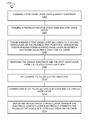
- FIG. 1 shows an integrated pMUT on CMOS at an early stage of manufacture according to one aspect of the present embodiments.
- FIG. 2 shows the integrated pMUT on CMOS after fusion bonding and removal of the carrier substrate according to one aspect of the present embodiments.
- FIG. 3 shows the integrated pMUT on CMOS after piezoelectric film stack deposition and patterning according to one aspect of the present embodiments.
- FIG. 4 shows the integrated pMUT on CMOS after gap fill oxide has been deposited and planarized according to one aspect of the present embodiments.
- FIG. 5 shows the integrated pMUT on CMOS after formation of a first electrical contact via and a second electrical contact via according to one aspect of the present embodiments.
- FIG. 6 shows the integrated pMUT on CMOS after deposition and patterning of an electrical contact layer according to one aspect of the present embodiments.
- FIG. 7 shows another integrated pMUT on CMOS at an early stage of manufacture according to one aspect of the present embodiments.
- FIG. 8 shows the integrated pMUT on CMOS after fusion bonding and removal of the carrier substrate according to one aspect of the present embodiments.
- FIG. 9 shows the integrated pMUT on CMOS after piezoelectric film stack patterning and deposition of gap fill oxide according to one aspect of the present embodiments.
- FIG. 10 shows the integrated pMUT on CMOS after formation of a first electrical contact via and a second electrical contact via according to one aspect of the present embodiments.
- FIG. 11 shows the integrated pMUT on CMOS after deposition and patterning of an electrical contact layer according to one aspect of the present embodiments.
- FIG. 12 shows an exemplary flow diagram for an integration of pMUT on CMOS according to one aspect of the present embodiments.
- FIG. 13 shows an exemplary flow diagram for another integration of pMUT on CMOS according to one aspect of the present embodiments.
- ordinal numbers e.g., first, second, third, etc. are used to distinguish or identify different elements or steps in a group of elements or steps, and do not supply a serial or numerical limitation on the elements or steps of the embodiments thereof.
- first, second, and “third” elements or steps need not necessarily appear in that order, and the embodiments thereof need not necessarily be limited to three elements or steps.
- any labels such as “left,” “right,” “front,” “back,” “top,” “middle,” “bottom,” “beside,” “forward,” “reverse,” “overlying,” “underlying,” “up,” “down,” or other similar terms such as “upper,” “lower,” “above,” “below, ” “under,” “between,” “over,” “vertical,” “horizontal,” “proximal,” “distal,” and the like are used for convenience and are not intended to imply, for example, any particular fixed location, orientation, or direction. Instead, such labels are used to reflect, for example, relative location, orientation, or directions. It should also be understood that the singular forms of “a,” “an,” and “the” include plural references unless the context clearly dictates otherwise.
- Terms such as “over,” “overlying,” “above,” “under,” etc. are understood to refer to elements that may be in direct contact or may have other elements in-between.
- two layers may be in overlying contact, wherein one layer is over another layer and the two layers physically contact.
- two layers may be separated by one or more layers, wherein a first layer is over a second layer and one or more intermediate layers are between the first and second layers, such that the first and second layers do not physically contact.
- Piezoelectric ultrasonic transducers have been miniaturized to form a MEMS device, referred to as a piezoelectric micromachined ultrasonic transducer (“pMUT”).
- MEMS pMUT wafers may be bonded to CMOS wafers using eutectic bonding method, however such processes can be costly.
- integration of CMOS and MEMS pMUT wafers is limited by alignment accuracy tolerances of wafer bonding process. Accordingly, a need has arisen to reduce the cost of CMOS and MEMS pMUT wafer integration, as well as improving alignment tolerances.
- Embodiments described herein address such needs by integrating a pMUT directly on a CMOS substrate using fusion bonding processes.
- a CMOS substrate 102 has been formed with a first metal electrode 104 and a second metal electrode 106 on the CMOS substrate 102 .
- a first fusion bond oxide 108 is deposited over the CMOS substrate 102 , the first metal electrode 104 and the second metal electrode 106 .
- a cavity 110 is formed in the first fusion bond oxide 108 , located over the first metal electrode 104 .
- one or more cavities 110 may be formed over one or more first metal electrodes 104 .
- the second metal electrode 106 remains covered by the first fusion bond oxide 108 .
- the CMOS substrate 102 includes many CMOS structures including, but not limited to, integrated circuit(s), transistor(s), substrate(s), electrical connection(s), metal electrode(s), the fusion bond oxide, etc.
- a carrier substrate 112 (e.g. handle substrate) includes a second fusion bond oxide 114 .
- the second fusion bond oxide 114 may be the same material as the first fusion bond oxide 108 or a different material.
- the carrier substrate 112 (e.g. handle substrate) and the second fusion bond oxide 114 do not contain any metal, and no features have been formed (e.g. no patterning) in either the carrier substrate 112 or the second fusion bond oxide 114 .
- the integrated pMUT on CMOS 100 after fusion bonding and removal of the carrier substrate 112 is shown according to one aspect of the present embodiments.
- the first fusion bond oxide 108 and the second fusion bond oxide 114 have been fusion bonded together to form a unified oxide layer 216 .
- the unified oxide layer 216 encloses the cavity 110 , thereby forming a membrane 218 (e.g. diaphragm) over the cavity 110 and a portion of the first metal electrode 104 .
- the carrier substrate 112 is removed (e.g. by grinding, etching, etc.) leaving the unified oxide layer 216 over the CMOS substrate 102 .
- the piezoelectric film stack 220 includes a seed layer 222 (e.g. aluminum nitride) overlying the unified oxide layer 216 , a first metal layer 224 (e.g. molybdenum) overlying the seed layer 222 , a piezoelectric layer 226 (e.g. aluminum nitride) overlying the first metal layer 224 , and a second metal layer 228 (e.g. molybdenum) overlying the piezoelectric layer 226 .
- the piezoelectric film stack 220 includes aluminum nitride, lead zirconate titanate, zinc oxide, polyvinylidene difluoride, and/or lithium niobate.
- the piezoelectric film stack 220 is patterned and formed, resulting in at least a portion of the piezoelectric film stack 220 remaining over the first metal electrode 104 .
- the piezoelectric film stack 220 does not overly the second metal electrode 106 after patterning.
- the piezoelectric film stack 220 is over the cavity 110 , the membrane 218 (e.g. diaphragm), and the unified oxide layer 216 (e.g. the first fusion bond oxide 108 and the second fusion bond oxide 114 fusion bonded together).
- the integrated pMUT on CMOS 100 after gap fill oxide has been deposited and planarized is shown according to one aspect of the present embodiments. Additional oxide (e.g. gap fill oxide) has been added to the unified oxide layer 216 and planarized.
- the gap fill oxide is deposited subsequent to patterning the piezoelectric film stack 220 .
- the unified oxide layer 216 surrounds the piezoelectric film stack 220 , leaving a top surface 430 of the piezoelectric film stack 220 exposed and free of the unified oxide layer 216 .
- the integrated pMUT on CMOS 100 after formation of a first electrical contact via 532 and a second electrical contact via 534 is shown according to one aspect of the present embodiments.
- the first electrical contact via 532 is formed (e.g. etched) into the piezoelectric film stack 220 .
- the second electrical contact via 534 is formed (e.g. etched) into the unified oxide layer 216 down to the second metal electrode 106 .
- the electrical contact layer 636 is deposited over the unified oxide layer 216 and the piezoelectric film stack 220 .
- the electrical contact layer 636 fills the first electrical contact via 532 and the second electrical contact via 534 , thereby electrically connecting the piezoelectric film stack 220 to the second metal electrode 106 on the CMOS substrate 102 .
- the electrical contact layer 636 and the piezoelectric film stack 220 are patterned. Such patterning defines electrical connections from the piezoelectric film stack 220 to one or more electrodes (e.g.
- first metal electrode 104 second metal electrode 106 , and/or other metal electrodes.
- the top and bottom electrode of piezoelectric film stack 220 is electrically connected to the electrodes on the CMOS substrate 102 without a eutectic bond.
- the fusion bonding process described above uses silicon oxide.
- cost is reduced by removing the use of silicon on insulator or polysilicon on insulator substrates used in eutectic bonding.
- the fusion bonding process described above does not rely on the accuracy of wafer-to-wafer bonding processes. Instead the wafers are bonded together prior to patterning, resulting in improved alignment accuracy between defined features.
- a CMOS substrate 702 has been formed with a first metal electrode 704 , a second metal electrode 706 , and a first fusion bond oxide 708 .
- a cavity 710 is formed in the first fusion bond oxide 708 .
- the cavity 710 is formed over the first metal electrode 704 .
- one or more cavities 710 may be formed over one or more first metal electrodes 704 .
- the second metal electrode 706 remains covered by the fusion bond oxide 708 .
- the CMOS substrate 702 includes many CMOS structures including, but not limited to, integrated circuit(s), transistor(s), substrate(s), electrical connection(s), metal electrode(s), the fusion bond oxide, etc.
- a stop oxide layer 738 is formed on a carrier substrate 712 (e.g. handle substrate).
- a piezoelectric film stack 720 is formed on the stop oxide layer 738 and includes a seed layer 722 (e.g. aluminum nitride) on the stop oxide layer 738 , a first metal layer 724 (e.g. molybdenum) on the seed layer 722 , a piezoelectric layer 726 (e.g. aluminum nitride) on the first metal layer 724 , and a second metal layer 728 (e.g. molybdenum) on the piezoelectric layer 226 .
- the piezoelectric film stack 720 includes aluminum nitride, lead zirconate titanate, zinc oxide, polyvinylidene difluoride, and/or lithium niobate.
- a second fusion bond oxide 714 is formed on the second metal layer 728 of the piezoelectric film stack 720 .
- the second fusion bond oxide 714 may be the same material as the first fusion bond oxide 708 or a different material. In various embodiments, no features have been formed in either the carrier substrate 712 or the second fusion bond oxide 714 .
- FIG. 8 the integrated pMUT on CMOS 700 after fusion bonding and removal of the carrier substrate 712 is shown according to one aspect of the present embodiments.
- the first fusion bond oxide 708 and the second fusion bond oxide 714 have been fusion bonded together to form a unified oxide layer 816 .
- the unified oxide layer 816 encloses the cavity 710 and forms a membrane 818 (e.g. diaphragm) over the cavity 710 and a portion of the first metal electrode 704 .
- the carrier substrate 712 and the stop oxide layer 738 are removed (e.g. by grinding, etching, etc.).
- the first metal layer 724 is over the piezoelectric layer 726 .
- the piezoelectric layer 726 is over the second metal layer 728 .
- the second metal layer 728 is over the unified oxide layer 816 (e.g. the first fusion bond oxide 708 and the second fusion bond oxide 714 fusion bonded together).
- the integrated pMUT on CMOS 700 after piezoelectric film stack 720 patterning and deposition of gap fill oxide is shown according to one aspect of the present embodiments.
- the piezoelectric film stack 720 is patterned and formed (e.g. by etching), resulting in at least a portion of the piezoelectric film stack 720 remaining over the first metal electrode 704 , the cavity 710 , the membrane 818 (e.g. diaphragm), and the unified oxide layer 816 (e.g. the first fusion bond oxide 708 and the second fusion bond oxide 714 fusion bonded together).
- the piezoelectric film stack 720 does not overly the second metal electrode 706 after patterning.
- additional oxide e.g. gap fill oxide
- the gap fill oxide is deposited subsequent to depositing and patterning the piezoelectric film stack 720 .
- the unified oxide layer 816 surrounds the piezoelectric film stack 720 , leaving a top surface 930 of the piezoelectric film stack 720 exposed and free of the unified oxide layer 816 .
- the integrated pMUT on CMOS 700 after formation of a first electrical contact via 1032 and a second electrical contact via 1034 is shown according to one aspect of the present embodiments.
- the first electrical contact via 1032 is formed (e.g. etched) into the piezoelectric film stack 720 .
- the second electrical contact via 1034 is formed (e.g. etched) into the unified oxide layer 816 down to the second metal electrode 706 .
- the electrical contact layer 1136 is deposited over the unified oxide layer 816 and the piezoelectric film stack 720 .
- the electrical contact layer 1136 fills the first electrical contact via 1032 and the second electrical contact via 1034 , thereby electrically connecting the piezoelectric film stack 720 to the second metal electrode 706 on the CMOS substrate 702 .
- the electrical contact layer 1136 and the piezoelectric film stack 720 are patterned. Such patterning defines electrical connections from the piezoelectric film stack 720 to one or more electrodes (e.g.
- first metal electrode 704 second metal electrode 706 , and/or other metal electrodes.
- the top and bottom electrodes of piezoelectric film stack 720 is electrically connected to the electrodes on the CMOS substrate 702 without a eutectic bond.
- the fusion bonding process described above uses silicon oxide.
- cost is reduced by removing the use of silicon on insulator or polysilicon on insulator substrates used in eutectic bonding.
- the fusion bonding process described above does not rely on the accuracy of wafer-to-wafer bonding processes. Instead the wafers are bonded together prior to patterning, resulting in improved alignment accuracy between defined features.
- FIG. 12 shows an exemplary flow diagram 1200 for the integration of pMUT on CMOS according to one aspect of the present embodiments.
- a first oxide layer on a handle substrate is fusion bonded to a second oxide layer on a CMOS, wherein the fusion bonding forms a unified oxide layer including a diaphragm overlying a cavity on the CMOS.
- the second fusion bond oxide on the carrier substrate is fusion bonded to the first fusion bond oxide.
- the fusion bonding forms the unified oxide layer that encloses the cavity, thereby forming a membrane (e.g. diaphragm) over the cavity on the CMOS.
- the handle substrate and the first oxide layer do not include any metal.
- the carrier substrate e.g. handle substrate
- the second fusion bond oxide do not contain any metal.
- the fusion bonding occurs prior to any patterning of the second oxide layer.
- no features have been formed (e.g. no patterning) in either the carrier substrate or the second fusion bond oxide.
- the handle substrate is removed leaving the unified oxide layer.
- the carrier substrate is removed (e.g. by grinding, etching, etc.) leaving the unified oxide layer over the CMOS substrate.
- a piezoelectric film stack is deposited over the unified oxide layer.
- the piezoelectric film stack is deposited over the unified oxide layer.
- the piezoelectric film stack includes the seed layer deposited over the unified oxide layer, the first metal layer deposited over the seed layer, the piezoelectric layer deposited over the first metal layer, and the second metal layer deposited over the piezoelectric layer.
- the seed layer and the piezoelectric layer include aluminum nitride.
- the first metal layer and the second metal layer include molybdenum.
- a gap fill oxide is deposited subsequent to depositing the piezoelectric film stack over the unified oxide layer.
- additional oxide e.g. gap fill oxide
- FIG. 4 additional oxide (e.g. gap fill oxide) has been added to the unified oxide layer and planarized subsequent to depositing and patterning the piezoelectric film stack.
- vias are formed in the piezoelectric film stack and the unified oxide layer.
- the first electrical contact via is formed (e.g. etched) into the piezoelectric film stack.
- the second electrical contact via is formed (e.g. etched) into the unified oxide layer down to the second metal electrode.
- an electrical contact layer is deposited, wherein the electrical contact layer electrically connects the piezoelectric film stack to an electrode on the CMOS.
- the electrical contact layer fills the first electrical contact via and the second electrical contact via, thereby electrically connecting the piezoelectric film stack to the second metal electrode on the CMOS.
- FIG. 13 shows an exemplary flow diagram 1300 for the integration of pMUT on CMOS according to one aspect of the present embodiments.
- a stop oxide layer is formed over a handle substrate.
- a stop oxide layer is formed on a carrier substrate (e.g. handle substrate).
- a piezoelectric film stack is formed over the stop oxide layer.
- a piezoelectric film stack is formed over the stop oxide layer and includes a seed layer deposited over the stop oxide layer, a first metal layer deposited over the seed layer, a piezoelectric layer deposited over the first metal layer, and a second metal layer deposited over the piezoelectric layer.
- the piezoelectric film stack includes aluminum nitride, lead zirconate titanate, zinc oxide, polyvinylidene difluoride, and/or lithium niobate.
- a first oxide layer on a CMOS is fusion bonded to a second oxide layer on the piezoelectric film stack, wherein the fusion bonding forms a unified oxide layer including a diaphragm overlying a cavity on the CMOS.
- the first fusion bond oxide on the CMOS and the second fusion bond oxide on the piezoelectric film stack have been fusion bonded together to form a unified oxide layer.
- the unified oxide layer encloses the cavity and forms a membrane (e.g. diaphragm) over the cavity.
- the handle substrate and the stop oxide layer are removed from the piezoelectric film stack.
- the carrier substrate and the stop oxide layer are removed (e.g. by grinding, etching, etc.).
- the piezoelectric film stack is patterned.
- the piezoelectric film stack is patterned and formed (e.g. by etching).
- a gap fill oxide is deposited and planarized subsequent to patterning the piezoelectric film stack.
- additional oxide e.g. gap fill oxide
- the gap fill oxide is deposited subsequent to depositing and patterning the piezoelectric film stack.
- the fusion bonding occurs prior to the patterning of the piezoelectric film stack.
- the first fusion bond oxide and the second fusion bond oxide have been fusion bonded together to form a unified oxide layer.
- the piezoelectric film stack is patterned and formed (e.g. by etching), resulting in at least a portion of the piezoelectric film stack remaining over the unified oxide layer (e.g. the first fusion bond oxide and the second fusion bond oxide fusion bonded together).
- vias are formed in the piezoelectric film stack and the unified oxide layer.
- the first electrical contact via is formed (e.g. etched) into the piezoelectric film stack.
- the second electrical contact via is formed (e.g. etched) into the unified oxide layer down to the second metal electrode.
- an electrical contact layer is deposited, wherein the electrical contact layer electrically connects the top and bottom electrodes of piezoelectric film stack to the electrodes on the CMOS.
- the electrical contact layer fills the first electrical contact via and the second electrical contact via, thereby electrically connecting the top and bottom electrodes of piezoelectric film stack to the metal electrodes on the CMOS substrate.
- the piezoelectric film stack is electrically connected to the CMOS without eutectic bonding.
- the electrical contact layer electrically connects the top and bottom electrodes of piezoelectric film stack to the metal electrodes on the CMOS substrate.
- the top and bottom electrodes piezoelectric film stack is electrically connected to the electrodes on the CMOS substrate without a eutectic bond.
Abstract
Provided herein is a method including bonding a first oxide layer on a handle substrate to a second oxide layer on a complementary metal oxide semiconductor (“CMOS”), wherein the fusion bonding forms a unified oxide layer including a diaphragm overlying a cavity on the CMOS. The handle substrate is removed leaving the unified oxide layer. A piezoelectric film stack is deposited over the unified oxide layer. Vias are formed in the piezoelectric film stack and the unified oxide layer. An electrical contact layer is deposited, wherein the electrical contact layer electrically connects the piezoelectric film stack to an electrode on the CMOS.
Description
This application claims the benefit and priority to the U.S. Provisional Patent Application Ser. No. 62/312,439 filed Mar. 23, 2016, entitled “AIN PMUT SENSOR MODULE INTEGRATION METHOD”, which is incorporated by reference in its entirety.
Piezoelectric materials convert energy between mechanical energy and electrical energy. A piezoelectric material generates electrical energy when mechanically deformed (e.g. under mechanical stress). On the other hand, a piezoelectric material may mechanically deform in response to electrical energy. For example, a piezoelectric material may vibrate in response to electrical energy, thereby acting as an ultrasonic transducer to generate acoustic waves. Piezoelectric materials may be used in micro-electro-mechanical system (“MEMS”) devices, for example, in fingerprint recognition.
Provided herein is a method including bonding a first oxide layer on a handle substrate to a second oxide layer on a complementary metal oxide semiconductor (“CMOS”), wherein the fusion bonding forms a unified oxide layer including a diaphragm overlying a cavity on the CMOS. The handle substrate is removed leaving the unified oxide layer. A piezoelectric film stack is deposited over the unified oxide layer. Vias are formed in the piezoelectric film stack and the unified oxide layer. An electrical contact layer is deposited, wherein the electrical contact layer electrically connects the piezoelectric film stack to an electrode on the CMOS. These and other features and advantages will be apparent from a reading of the following detailed description.
Before various embodiments are described in greater detail, it should be understood that the embodiments are not limiting, as elements in such embodiments may vary. It should likewise be understood that a particular embodiment described and/or illustrated herein has elements which may be readily separated from the particular embodiment and optionally combined with any of several other embodiments or substituted for elements in any of several other embodiments described herein.
It should also be understood that the terminology used herein is for the purpose of describing the certain concepts, and the terminology is not intended to be limiting. Unless defined otherwise, all technical and scientific terms used herein have the same meaning as commonly understood in the art to which the embodiments pertain.
Unless indicated otherwise, ordinal numbers (e.g., first, second, third, etc.) are used to distinguish or identify different elements or steps in a group of elements or steps, and do not supply a serial or numerical limitation on the elements or steps of the embodiments thereof. For example, “first,” “second,” and “third” elements or steps need not necessarily appear in that order, and the embodiments thereof need not necessarily be limited to three elements or steps. It should also be understood that, unless indicated otherwise, any labels such as “left,” “right,” “front,” “back,” “top,” “middle,” “bottom,” “beside,” “forward,” “reverse,” “overlying,” “underlying,” “up,” “down,” or other similar terms such as “upper,” “lower,” “above,” “below, ” “under,” “between,” “over,” “vertical,” “horizontal,” “proximal,” “distal,” and the like are used for convenience and are not intended to imply, for example, any particular fixed location, orientation, or direction. Instead, such labels are used to reflect, for example, relative location, orientation, or directions. It should also be understood that the singular forms of “a,” “an,” and “the” include plural references unless the context clearly dictates otherwise.
Terms such as “over,” “overlying,” “above,” “under,” etc. are understood to refer to elements that may be in direct contact or may have other elements in-between. For example, two layers may be in overlying contact, wherein one layer is over another layer and the two layers physically contact. In another example, two layers may be separated by one or more layers, wherein a first layer is over a second layer and one or more intermediate layers are between the first and second layers, such that the first and second layers do not physically contact.
Piezoelectric ultrasonic transducers have been miniaturized to form a MEMS device, referred to as a piezoelectric micromachined ultrasonic transducer (“pMUT”). MEMS pMUT wafers may be bonded to CMOS wafers using eutectic bonding method, however such processes can be costly. In addition, integration of CMOS and MEMS pMUT wafers is limited by alignment accuracy tolerances of wafer bonding process. Accordingly, a need has arisen to reduce the cost of CMOS and MEMS pMUT wafer integration, as well as improving alignment tolerances. Embodiments described herein address such needs by integrating a pMUT directly on a CMOS substrate using fusion bonding processes.
Referring now to FIG. 1 , an integrated pMUT on CMOS 100 at an early stage of manufacture is shown according to one aspect of the present embodiments. A CMOS substrate 102 has been formed with a first metal electrode 104 and a second metal electrode 106 on the CMOS substrate 102. A first fusion bond oxide 108 is deposited over the CMOS substrate 102, the first metal electrode 104 and the second metal electrode 106. A cavity 110 is formed in the first fusion bond oxide 108, located over the first metal electrode 104. In various embodiments, one or more cavities 110 may be formed over one or more first metal electrodes 104. At this stage of manufacture, the second metal electrode 106 remains covered by the first fusion bond oxide 108. It is understood that the CMOS substrate 102 includes many CMOS structures including, but not limited to, integrated circuit(s), transistor(s), substrate(s), electrical connection(s), metal electrode(s), the fusion bond oxide, etc.
A carrier substrate 112 (e.g. handle substrate) includes a second fusion bond oxide 114. The second fusion bond oxide 114 may be the same material as the first fusion bond oxide 108 or a different material. In various embodiments, the carrier substrate 112 (e.g. handle substrate) and the second fusion bond oxide 114 do not contain any metal, and no features have been formed (e.g. no patterning) in either the carrier substrate 112 or the second fusion bond oxide 114.
Referring now to FIG. 2 , the integrated pMUT on CMOS 100 after fusion bonding and removal of the carrier substrate 112 is shown according to one aspect of the present embodiments. The first fusion bond oxide 108 and the second fusion bond oxide 114 have been fusion bonded together to form a unified oxide layer 216. The unified oxide layer 216 encloses the cavity 110, thereby forming a membrane 218 (e.g. diaphragm) over the cavity 110 and a portion of the first metal electrode 104. After the fusion bonding and formation of the unified oxide layer 216, the carrier substrate 112 is removed (e.g. by grinding, etching, etc.) leaving the unified oxide layer 216 over the CMOS substrate 102.
Referring now to FIG. 3 , the integrated pMUT on CMOS 100 after piezoelectric film stack 220 deposition and patterning is shown according to one aspect of the present embodiments. The piezoelectric film stack 220 includes a seed layer 222 (e.g. aluminum nitride) overlying the unified oxide layer 216, a first metal layer 224 (e.g. molybdenum) overlying the seed layer 222, a piezoelectric layer 226 (e.g. aluminum nitride) overlying the first metal layer 224, and a second metal layer 228 (e.g. molybdenum) overlying the piezoelectric layer 226. In various embodiments, the piezoelectric film stack 220 includes aluminum nitride, lead zirconate titanate, zinc oxide, polyvinylidene difluoride, and/or lithium niobate.
After layer deposition, the piezoelectric film stack 220 is patterned and formed, resulting in at least a portion of the piezoelectric film stack 220 remaining over the first metal electrode 104. In various embodiments, the piezoelectric film stack 220 does not overly the second metal electrode 106 after patterning. As such, the piezoelectric film stack 220 is over the cavity 110, the membrane 218 (e.g. diaphragm), and the unified oxide layer 216 (e.g. the first fusion bond oxide 108 and the second fusion bond oxide 114 fusion bonded together).
Referring now to FIG. 4 , the integrated pMUT on CMOS 100 after gap fill oxide has been deposited and planarized is shown according to one aspect of the present embodiments. Additional oxide (e.g. gap fill oxide) has been added to the unified oxide layer 216 and planarized. In various embodiments, the gap fill oxide is deposited subsequent to patterning the piezoelectric film stack 220. As a result the unified oxide layer 216 surrounds the piezoelectric film stack 220, leaving a top surface 430 of the piezoelectric film stack 220 exposed and free of the unified oxide layer 216.
Referring now to FIG. 5 , the integrated pMUT on CMOS 100 after formation of a first electrical contact via 532 and a second electrical contact via 534 is shown according to one aspect of the present embodiments. In various embodiments, the first electrical contact via 532 is formed (e.g. etched) into the piezoelectric film stack 220. In addition, the second electrical contact via 534 is formed (e.g. etched) into the unified oxide layer 216 down to the second metal electrode 106.
Referring now to FIG. 6 , the integrated pMUT on CMOS 100 after deposition and patterning of an electrical contact layer 636 is shown according to one aspect of the present embodiments. The electrical contact layer 636 is deposited over the unified oxide layer 216 and the piezoelectric film stack 220. The electrical contact layer 636 fills the first electrical contact via 532 and the second electrical contact via 534, thereby electrically connecting the piezoelectric film stack 220 to the second metal electrode 106 on the CMOS substrate 102. In various embodiments, the electrical contact layer 636 and the piezoelectric film stack 220 are patterned. Such patterning defines electrical connections from the piezoelectric film stack 220 to one or more electrodes (e.g. first metal electrode 104, second metal electrode 106, and/or other metal electrodes). As a result of the fusion bonding and layer depositions described above, the top and bottom electrode of piezoelectric film stack 220 is electrically connected to the electrodes on the CMOS substrate 102 without a eutectic bond.
As a result of the integrated pMUT on CMOS fabrication described above, expensive eutectic bonding processes (e.g. Al—Ge eutectic bonding) can be avoided. In addition, process throughput can be improved by removing the relatively lengthy eutectic bonding process. The fusion bonding process described above addresses these concerns by reducing expense and improving process throughput.
In addition, the fusion bonding process described above uses silicon oxide. As a result, cost is reduced by removing the use of silicon on insulator or polysilicon on insulator substrates used in eutectic bonding.
Furthermore, the fusion bonding process described above does not rely on the accuracy of wafer-to-wafer bonding processes. Instead the wafers are bonded together prior to patterning, resulting in improved alignment accuracy between defined features.
Referring now to FIG. 7 , an integrated pMUT on CMOS 700 at an early stage of manufacture is shown according to one aspect of the present embodiments. A CMOS substrate 702 has been formed with a first metal electrode 704, a second metal electrode 706, and a first fusion bond oxide 708. A cavity 710 is formed in the first fusion bond oxide 708. The cavity 710 is formed over the first metal electrode 704. In various embodiments, one or more cavities 710 may be formed over one or more first metal electrodes 704. At this stage of manufacture, the second metal electrode 706 remains covered by the fusion bond oxide 708. It is understood that the CMOS substrate 702 includes many CMOS structures including, but not limited to, integrated circuit(s), transistor(s), substrate(s), electrical connection(s), metal electrode(s), the fusion bond oxide, etc.
A stop oxide layer 738 is formed on a carrier substrate 712 (e.g. handle substrate). A piezoelectric film stack 720 is formed on the stop oxide layer 738 and includes a seed layer 722 (e.g. aluminum nitride) on the stop oxide layer 738, a first metal layer 724 (e.g. molybdenum) on the seed layer 722, a piezoelectric layer 726 (e.g. aluminum nitride) on the first metal layer 724, and a second metal layer 728 (e.g. molybdenum) on the piezoelectric layer 226. In various embodiments, the piezoelectric film stack 720 includes aluminum nitride, lead zirconate titanate, zinc oxide, polyvinylidene difluoride, and/or lithium niobate.
A second fusion bond oxide 714 is formed on the second metal layer 728 of the piezoelectric film stack 720. The second fusion bond oxide 714 may be the same material as the first fusion bond oxide 708 or a different material. In various embodiments, no features have been formed in either the carrier substrate 712 or the second fusion bond oxide 714.
Referring now to FIG. 8 , the integrated pMUT on CMOS 700 after fusion bonding and removal of the carrier substrate 712 is shown according to one aspect of the present embodiments. The first fusion bond oxide 708 and the second fusion bond oxide 714 have been fusion bonded together to form a unified oxide layer 816. The unified oxide layer 816 encloses the cavity 710 and forms a membrane 818 (e.g. diaphragm) over the cavity 710 and a portion of the first metal electrode 704. After the fusion bonding and formation of the unified oxide layer 816, the carrier substrate 712 and the stop oxide layer 738 are removed (e.g. by grinding, etching, etc.).
The removal leaves the piezoelectric film stack 720 including the first metal layer 724, the piezoelectric layer 726, and the second metal layer 728. The first metal layer 724 is over the piezoelectric layer 726. The piezoelectric layer 726 is over the second metal layer 728. The second metal layer 728 is over the unified oxide layer 816 (e.g. the first fusion bond oxide 708 and the second fusion bond oxide 714 fusion bonded together).
Referring now to FIG. 9 , the integrated pMUT on CMOS 700 after piezoelectric film stack 720 patterning and deposition of gap fill oxide is shown according to one aspect of the present embodiments. The piezoelectric film stack 720 is patterned and formed (e.g. by etching), resulting in at least a portion of the piezoelectric film stack 720 remaining over the first metal electrode 704, the cavity 710, the membrane 818 (e.g. diaphragm), and the unified oxide layer 816 (e.g. the first fusion bond oxide 708 and the second fusion bond oxide 714 fusion bonded together). In various embodiments, the piezoelectric film stack 720 does not overly the second metal electrode 706 after patterning.
After the patterning of the piezoelectric film stack 720, additional oxide (e.g. gap fill oxide) has been deposited and added to the unified oxide layer 816 and planarized. In various embodiments, the gap fill oxide is deposited subsequent to depositing and patterning the piezoelectric film stack 720. As a result the unified oxide layer 816 surrounds the piezoelectric film stack 720, leaving a top surface 930 of the piezoelectric film stack 720 exposed and free of the unified oxide layer 816.
Referring now to FIG. 10 , the integrated pMUT on CMOS 700 after formation of a first electrical contact via 1032 and a second electrical contact via 1034 is shown according to one aspect of the present embodiments. In various embodiments, the first electrical contact via 1032 is formed (e.g. etched) into the piezoelectric film stack 720. In addition, the second electrical contact via 1034 is formed (e.g. etched) into the unified oxide layer 816 down to the second metal electrode 706.
Referring now to FIG. 11 , the integrated pMUT on CMOS 700 after deposition and patterning of an electrical contact layer 1136 is shown according to one aspect of the present embodiments. The electrical contact layer 1136 is deposited over the unified oxide layer 816 and the piezoelectric film stack 720. The electrical contact layer 1136 fills the first electrical contact via 1032 and the second electrical contact via 1034, thereby electrically connecting the piezoelectric film stack 720 to the second metal electrode 706 on the CMOS substrate 702. In various embodiments, the electrical contact layer 1136 and the piezoelectric film stack 720 are patterned. Such patterning defines electrical connections from the piezoelectric film stack 720 to one or more electrodes (e.g. first metal electrode 704, second metal electrode 706, and/or other metal electrodes). As a result of the fusion bonding and layer depositions described above, the top and bottom electrodes of piezoelectric film stack 720 is electrically connected to the electrodes on the CMOS substrate 702 without a eutectic bond.
As a result of the integrated pMUT on CMOS fabrication described above, expensive eutectic bonding processes (e.g. Al—Ge eutectic bonding) can be avoided. In addition, process throughput can be improved by removing the relatively lengthy eutectic bonding process. The fusion bonding process described above addresses these concerns by reducing expense and improving process throughput.
In addition, the fusion bonding process described above uses silicon oxide. As a result, cost is reduced by removing the use of silicon on insulator or polysilicon on insulator substrates used in eutectic bonding.
Furthermore, the fusion bonding process described above does not rely on the accuracy of wafer-to-wafer bonding processes. Instead the wafers are bonded together prior to patterning, resulting in improved alignment accuracy between defined features.
In some embodiments, the handle substrate and the first oxide layer do not include any metal. For example, in FIG. 1 the carrier substrate (e.g. handle substrate) and the second fusion bond oxide do not contain any metal. In various embodiments, the fusion bonding occurs prior to any patterning of the second oxide layer. For example, in FIG. 1 no features have been formed (e.g. no patterning) in either the carrier substrate or the second fusion bond oxide.
At block 1204, the handle substrate is removed leaving the unified oxide layer. For example, in FIG. 2 the carrier substrate is removed (e.g. by grinding, etching, etc.) leaving the unified oxide layer over the CMOS substrate.
At a block 1206, a piezoelectric film stack is deposited over the unified oxide layer. For example, in FIG. 3 the piezoelectric film stack is deposited over the unified oxide layer. In some embodiments, the piezoelectric film stack includes the seed layer deposited over the unified oxide layer, the first metal layer deposited over the seed layer, the piezoelectric layer deposited over the first metal layer, and the second metal layer deposited over the piezoelectric layer. In various embodiments, the seed layer and the piezoelectric layer include aluminum nitride. In further embodiments, the first metal layer and the second metal layer include molybdenum.
In some embodiments, a gap fill oxide is deposited subsequent to depositing the piezoelectric film stack over the unified oxide layer. For example, in FIG. 4 additional oxide (e.g. gap fill oxide) has been added to the unified oxide layer and planarized subsequent to depositing and patterning the piezoelectric film stack.
At a block 1208, vias are formed in the piezoelectric film stack and the unified oxide layer. For example, in FIG. 5 the first electrical contact via is formed (e.g. etched) into the piezoelectric film stack. In addition, the second electrical contact via is formed (e.g. etched) into the unified oxide layer down to the second metal electrode.
At a block 1210, an electrical contact layer is deposited, wherein the electrical contact layer electrically connects the piezoelectric film stack to an electrode on the CMOS. For example, in FIG. 6 the electrical contact layer fills the first electrical contact via and the second electrical contact via, thereby electrically connecting the piezoelectric film stack to the second metal electrode on the CMOS.
At block 1304, a piezoelectric film stack is formed over the stop oxide layer. For example, in FIG. 7 a piezoelectric film stack is formed over the stop oxide layer and includes a seed layer deposited over the stop oxide layer, a first metal layer deposited over the seed layer, a piezoelectric layer deposited over the first metal layer, and a second metal layer deposited over the piezoelectric layer. In various embodiments, the piezoelectric film stack includes aluminum nitride, lead zirconate titanate, zinc oxide, polyvinylidene difluoride, and/or lithium niobate.
At a block 1306, a first oxide layer on a CMOS is fusion bonded to a second oxide layer on the piezoelectric film stack, wherein the fusion bonding forms a unified oxide layer including a diaphragm overlying a cavity on the CMOS. For example, in FIG. 8 the first fusion bond oxide on the CMOS and the second fusion bond oxide on the piezoelectric film stack have been fusion bonded together to form a unified oxide layer. The unified oxide layer encloses the cavity and forms a membrane (e.g. diaphragm) over the cavity.
At a block 1308, the handle substrate and the stop oxide layer are removed from the piezoelectric film stack. For example, in FIG. 8 the carrier substrate and the stop oxide layer are removed (e.g. by grinding, etching, etc.).
At a block 1310, the piezoelectric film stack is patterned. For example, in FIG. 9 the piezoelectric film stack is patterned and formed (e.g. by etching). In some embodiments, a gap fill oxide is deposited and planarized subsequent to patterning the piezoelectric film stack. For example, in FIG. 9 after the patterning of the piezoelectric film stack, additional oxide (e.g. gap fill oxide) has been deposited and added to the unified oxide layer and planarized. In various embodiments, the gap fill oxide is deposited subsequent to depositing and patterning the piezoelectric film stack.
In some embodiments, the fusion bonding occurs prior to the patterning of the piezoelectric film stack. For example, in FIGS. 8 and 9 the first fusion bond oxide and the second fusion bond oxide have been fusion bonded together to form a unified oxide layer. Thereafter, the piezoelectric film stack is patterned and formed (e.g. by etching), resulting in at least a portion of the piezoelectric film stack remaining over the unified oxide layer (e.g. the first fusion bond oxide and the second fusion bond oxide fusion bonded together).
At a block 1312, vias are formed in the piezoelectric film stack and the unified oxide layer. For example, in FIG. 10 the first electrical contact via is formed (e.g. etched) into the piezoelectric film stack. In addition, the second electrical contact via is formed (e.g. etched) into the unified oxide layer down to the second metal electrode.
At a block 1314, an electrical contact layer is deposited, wherein the electrical contact layer electrically connects the top and bottom electrodes of piezoelectric film stack to the electrodes on the CMOS. For example, in FIG. 11 the electrical contact layer fills the first electrical contact via and the second electrical contact via, thereby electrically connecting the top and bottom electrodes of piezoelectric film stack to the metal electrodes on the CMOS substrate.
In some embodiments, the piezoelectric film stack is electrically connected to the CMOS without eutectic bonding. For example, in FIG. 11 the electrical contact layer electrically connects the top and bottom electrodes of piezoelectric film stack to the metal electrodes on the CMOS substrate. As a result of the fusion bonding and layer depositions described above, the top and bottom electrodes piezoelectric film stack is electrically connected to the electrodes on the CMOS substrate without a eutectic bond.
While the embodiments have been described and/or illustrated by means of particular examples, and while these embodiments and/or examples have been described in considerable detail, it is not the intention of the Applicants to restrict or in any way limit the scope of the embodiments to such detail. Additional adaptations and/or modifications of the embodiments may readily appear, and, in its broader aspects, the embodiments may encompass these adaptations and/or modifications. Accordingly, departures may be made from the foregoing embodiments and/or examples without departing from the scope of the concepts described herein. The implementations described above and other implementations are within the scope of the following claims.
Claims (14)
1. A method comprising:
fusion bonding a first oxide layer on a complementary metal oxide semiconductor (CMOS) to a second oxide layer on a handle substrate, wherein the fusion bonding forms a unified oxide layer including a diaphragm overlying a cavity on the CMOS;
removing the handle substrate leaving the unified oxide layer;
depositing a piezoelectric film stack over the unified oxide layer;
forming vias in the piezoelectric film stack and the unified oxide layer; and
depositing an electrical contact layer, wherein the electrical contact layer electrically connects the piezoelectric film stack to an electrode on the CMOS.
2. The method of claim 1 , wherein depositing the piezoelectric film stack includes:
depositing a seed layer over the unified oxide layer;
depositing a first metal layer over the seed layer;
depositing a piezoelectric layer over the first metal layer; and
depositing a second metal layer over the piezoelectric layer.
3. The method of claim 2 , wherein
the seed layer and the piezoelectric layer include aluminum nitride, and
the first metal layer and the second metal layer include molybdenum.
4. The method of claim 1 , further comprising depositing a gap fill oxide subsequent to the depositing the piezoelectric film stack over the unified oxide layer.
5. The method of claim 4 , further comprising planarizing the gap fill oxide.
6. The method of claim 1 , wherein the handle substrate and the second oxide layer do not include any metal.
7. The method of claim 1 , wherein the fusion bonding occurs prior to any patterning of the second oxide layer.
8. A method comprising:
forming a stop oxide layer over a handle substrate;
forming a piezoelectric film stack over the stop oxide layer;
fusion bonding a first oxide layer on a complementary metal oxide semiconductor (CMOS) to a second oxide layer on the piezoelectric film stack, wherein the fusion bonding forms a unified oxide layer including a diaphragm overlying a cavity on the CMOS;
removing the handle substrate and the stop oxide layer from the piezoelectric film stack;
patterning the piezoelectric film stack;
forming vias in the piezoelectric film stack and the unified oxide layer; and
depositing an electrical contact layer, wherein the electrical contact layer electrically connects the piezoelectric film stack to an electrode on the CMOS.
9. The method of claim 8 , wherein depositing the piezoelectric film stack includes:
depositing a seed layer over the stop oxide layer;
depositing a first metal layer over the seed layer;
depositing a piezoelectric layer over the first metal layer; and
depositing a second metal layer over the piezoelectric layer.
10. The method of claim 8 , wherein the piezoelectric film stack includes aluminum nitride, lead zirconate titanate, zinc oxide, polyvinylidene difluoride, or lithium niobate.
11. The method of claim 8 , further comprising depositing a gap fill oxide subsequent to the patterning the piezoelectric film stack.
12. The method of claim 11 , further comprising planarizing the gap fill oxide.
13. The method of claim 8 , wherein the fusion bonding occurs prior to the patterning of the piezoelectric film stack.
14. The method of claim 8 , wherein the piezoelectric film stack is electrically connected to the CMOS without eutectic bonding.
Priority Applications (1)
| Application Number | Priority Date | Filing Date | Title |
|---|---|---|---|
| US15/457,832 US9975763B2 (en) | 2016-03-23 | 2017-03-13 | Integration of AIN ultrasonic transducer on a CMOS substrate using fusion bonding process |
Applications Claiming Priority (2)
| Application Number | Priority Date | Filing Date | Title |
|---|---|---|---|
| US201662312439P | 2016-03-23 | 2016-03-23 | |
| US15/457,832 US9975763B2 (en) | 2016-03-23 | 2017-03-13 | Integration of AIN ultrasonic transducer on a CMOS substrate using fusion bonding process |
Publications (2)
| Publication Number | Publication Date |
|---|---|
| US20170275158A1 US20170275158A1 (en) | 2017-09-28 |
| US9975763B2 true US9975763B2 (en) | 2018-05-22 |
Family
ID=58428379
Family Applications (1)
| Application Number | Title | Priority Date | Filing Date |
|---|---|---|---|
| US15/457,832 Active US9975763B2 (en) | 2016-03-23 | 2017-03-13 | Integration of AIN ultrasonic transducer on a CMOS substrate using fusion bonding process |
Country Status (4)
| Country | Link |
|---|---|
| US (1) | US9975763B2 (en) |
| CN (1) | CN108886089B (en) |
| TW (1) | TWI664755B (en) |
| WO (1) | WO2017165146A1 (en) |
Families Citing this family (9)
| Publication number | Priority date | Publication date | Assignee | Title |
|---|---|---|---|---|
| MY191624A (en) | 2017-09-29 | 2022-07-04 | Silterra Malaysia Sdn Bhd | Monolithic integration of pmut on cmos |
| US10988376B2 (en) * | 2017-12-13 | 2021-04-27 | Vanguard International Semiconductor Singapore Pte. Ltd. | Monolithic integration of piezoelectric micromachined ultrasonic transducers and CMOS and method for producing the same |
| FR3077163B1 (en) | 2018-01-22 | 2021-08-27 | Soitec Silicon On Insulator | DESIGN AND MANUFACTURING METHODS OF A DEVICE INCLUDING A NETWORK OF MICRO-FACTORY ELEMENTS, A DEVICE OBTAINED AS A RESULT OF SUCH METHODS |
| US11701689B2 (en) | 2018-07-31 | 2023-07-18 | Resonant Acoustics International Inc. | Ultrasonic transducer |
| US11329098B2 (en) * | 2018-11-08 | 2022-05-10 | Vanguard International Semiconductor Singapore Pte. Ltd. | Piezoelectric micromachined ultrasonic transducers and methods for fabricating thereof |
| EP3918886A4 (en) * | 2019-01-29 | 2022-11-02 | Butterfly Network, Inc. | Packaging structures and packaging methods for ultrasound-on-chip devices |
| CN112115753B (en) | 2019-07-22 | 2023-12-19 | 中芯集成电路(宁波)有限公司 | Fingerprint identification module, manufacturing method thereof and electronic equipment |
| CN110523607B (en) * | 2019-07-31 | 2020-08-18 | 西安交通大学 | Piezoelectric transmitting capacitance sensing high-performance MUT unit and preparation method thereof |
| CN113560158B (en) * | 2021-08-27 | 2022-06-10 | 南京声息芯影科技有限公司 | Piezoelectric micromechanical ultrasonic transducer, array chip and manufacturing method |
Citations (8)
| Publication number | Priority date | Publication date | Assignee | Title |
|---|---|---|---|---|
| US20030199105A1 (en) * | 2002-04-22 | 2003-10-23 | Kub Francis J. | Method for making piezoelectric resonator and surface acoustic wave device using hydrogen implant layer splitting |
| US8610336B1 (en) * | 2011-09-30 | 2013-12-17 | Integrated Device Technology Inc | Microelectromechanical resonators having resistive heating elements therein configured to provide frequency tuning through convective heating of resonator bodies |
| US20140018126A1 (en) * | 2011-04-01 | 2014-01-16 | Renesas Electronics Corporation | Semiconductor device, manufacturing method of the same, and mobile phone |
| US20140232241A1 (en) * | 2013-02-15 | 2014-08-21 | Arman HAJATI | Piezoelectric array employing integrated mems switches |
| TW201517246A (en) | 2013-09-19 | 2015-05-01 | Invensense Inc | Aluminum nitride (AIN) devices with infrared absorption structural layer |
| US20150298965A1 (en) | 2012-11-28 | 2015-10-22 | Invensense, Inc. | ALUMINUM NITRIDE (AlN) DEVICES WITH INFRARED ABSORPTION STRUCTURAL LAYER |
| US20150357375A1 (en) | 2012-11-28 | 2015-12-10 | Invensense, Inc. | Integrated piezoelectric microelectromechanical ultrasound transducer (pmut) on integrated circuit (ic) for fingerprint sensing |
| TW201606849A (en) | 2014-06-13 | 2016-02-16 | 英特爾股份有限公司 | Surface encapsulation for wafer bonding |
Family Cites Families (2)
| Publication number | Priority date | Publication date | Assignee | Title |
|---|---|---|---|---|
| US9533873B2 (en) * | 2013-02-05 | 2017-01-03 | Butterfly Network, Inc. | CMOS ultrasonic transducers and related apparatus and methods |
| EP3757884A1 (en) * | 2014-09-08 | 2020-12-30 | InvenSense, Inc. | Integrated piezoelectric microelectromechanical ultrasound transducer (pmut) on integrated circuit (ic) for fingerprint sensing |
-
2017
- 2017-03-13 CN CN201780019280.2A patent/CN108886089B/en active Active
- 2017-03-13 WO PCT/US2017/022201 patent/WO2017165146A1/en active Application Filing
- 2017-03-13 US US15/457,832 patent/US9975763B2/en active Active
- 2017-03-13 TW TW106108194A patent/TWI664755B/en active
Patent Citations (8)
| Publication number | Priority date | Publication date | Assignee | Title |
|---|---|---|---|---|
| US20030199105A1 (en) * | 2002-04-22 | 2003-10-23 | Kub Francis J. | Method for making piezoelectric resonator and surface acoustic wave device using hydrogen implant layer splitting |
| US20140018126A1 (en) * | 2011-04-01 | 2014-01-16 | Renesas Electronics Corporation | Semiconductor device, manufacturing method of the same, and mobile phone |
| US8610336B1 (en) * | 2011-09-30 | 2013-12-17 | Integrated Device Technology Inc | Microelectromechanical resonators having resistive heating elements therein configured to provide frequency tuning through convective heating of resonator bodies |
| US20150298965A1 (en) | 2012-11-28 | 2015-10-22 | Invensense, Inc. | ALUMINUM NITRIDE (AlN) DEVICES WITH INFRARED ABSORPTION STRUCTURAL LAYER |
| US20150357375A1 (en) | 2012-11-28 | 2015-12-10 | Invensense, Inc. | Integrated piezoelectric microelectromechanical ultrasound transducer (pmut) on integrated circuit (ic) for fingerprint sensing |
| US20140232241A1 (en) * | 2013-02-15 | 2014-08-21 | Arman HAJATI | Piezoelectric array employing integrated mems switches |
| TW201517246A (en) | 2013-09-19 | 2015-05-01 | Invensense Inc | Aluminum nitride (AIN) devices with infrared absorption structural layer |
| TW201606849A (en) | 2014-06-13 | 2016-02-16 | 英特爾股份有限公司 | Surface encapsulation for wafer bonding |
Non-Patent Citations (1)
| Title |
|---|
| PCT International Search Report and Written Opinion dated Jun. 23, 2017 in International Application No. PCT/US2017/022201. 12 pages. |
Also Published As
| Publication number | Publication date |
|---|---|
| TWI664755B (en) | 2019-07-01 |
| US20170275158A1 (en) | 2017-09-28 |
| TW201739074A (en) | 2017-11-01 |
| CN108886089A (en) | 2018-11-23 |
| CN108886089B (en) | 2023-04-18 |
| WO2017165146A1 (en) | 2017-09-28 |
Similar Documents
| Publication | Publication Date | Title |
|---|---|---|
| US9975763B2 (en) | Integration of AIN ultrasonic transducer on a CMOS substrate using fusion bonding process | |
| US8402831B2 (en) | Monolithic integrated CMUTs fabricated by low-temperature wafer bonding | |
| US8222065B1 (en) | Method and system for forming a capacitive micromachined ultrasonic transducer | |
| US10335827B2 (en) | Ultrasonic transducer device with through-substrate via | |
| JP5876500B2 (en) | Ultrasonic vibrator forming method and related apparatus | |
| US8209857B2 (en) | Method of making a thin film device | |
| US10829364B2 (en) | MEMS transducer and method for manufacturing the same | |
| US9604255B2 (en) | Method, apparatus and system for a transferable micromachined piezoelectric transducer array | |
| CN108764087B (en) | Electronic device, ultrasonic fingerprint identification device and manufacturing method thereof | |
| US11504958B2 (en) | Method for transferring at least one layer of material from a first substrate to a second substrate | |
| JP2013518530A (en) | Method for forming a piezoelectric ultrasonic transducer and associated apparatus | |
| US9475092B2 (en) | Electro-acoustic transducer and method of manufacturing the same | |
| US8858447B2 (en) | Ultrasonic transducer and method of manufacturing the same | |
| TW202122338A (en) | Semiconductor device and forming method thereof | |
| US9873136B2 (en) | Ultrasonic transducer and method of manufacturing the same | |
| US10745270B2 (en) | Actuator layer patterning with topography | |
| US11897759B2 (en) | Semiconductor device and method for forming the same | |
| US20230354714A1 (en) | Micromechanical component, sound transducer device, and method for producing a micromechanical component | |
| JP2009233836A (en) | Mems and method for manufacturing mems | |
| CN111640855A (en) | Piezoelectric ultrasonic fingerprint sensor substrate, method of manufacturing the same, and method of manufacturing sensor | |
| CN117548320A (en) | Micromechanical ultrasonic transducer structure with double PMUTs arranged on same side of substrate and manufacturing method thereof | |
| CN111446360A (en) | Ultrasonic transducer preparation method, ultrasonic transducer and information acquisition element |
Legal Events
| Date | Code | Title | Description |
|---|---|---|---|
| AS | Assignment |
Owner name: INVENSENSE, INC., CALIFORNIA Free format text: ASSIGNMENT OF ASSIGNORS INTEREST;ASSIGNORS:SHIN, JONG IL;SMEYS, PETER;SHIN, JONGWOO;SIGNING DATES FROM 20170307 TO 20170404;REEL/FRAME:043083/0600 |
|
| STCF | Information on status: patent grant |
Free format text: PATENTED CASE |
|
| MAFP | Maintenance fee payment |
Free format text: PAYMENT OF MAINTENANCE FEE, 4TH YEAR, LARGE ENTITY (ORIGINAL EVENT CODE: M1551); ENTITY STATUS OF PATENT OWNER: LARGE ENTITY Year of fee payment: 4 |