US9965119B2 - High-sensitivity self-capacitance in-cell touch display panel device - Google Patents
High-sensitivity self-capacitance in-cell touch display panel device Download PDFInfo
- Publication number
- US9965119B2 US9965119B2 US14/932,496 US201514932496A US9965119B2 US 9965119 B2 US9965119 B2 US 9965119B2 US 201514932496 A US201514932496 A US 201514932496A US 9965119 B2 US9965119 B2 US 9965119B2
- Authority
- US
- United States
- Prior art keywords
- capacitance
- layer
- sensing
- substrate
- panel device
- Prior art date
- Legal status (The legal status is an assumption and is not a legal conclusion. Google has not performed a legal analysis and makes no representation as to the accuracy of the status listed.)
- Active, expires
Links
Images


Classifications
-
- G—PHYSICS
- G06—COMPUTING; CALCULATING OR COUNTING
- G06F—ELECTRIC DIGITAL DATA PROCESSING
- G06F3/00—Input arrangements for transferring data to be processed into a form capable of being handled by the computer; Output arrangements for transferring data from processing unit to output unit, e.g. interface arrangements
- G06F3/01—Input arrangements or combined input and output arrangements for interaction between user and computer
- G06F3/03—Arrangements for converting the position or the displacement of a member into a coded form
- G06F3/041—Digitisers, e.g. for touch screens or touch pads, characterised by the transducing means
- G06F3/044—Digitisers, e.g. for touch screens or touch pads, characterised by the transducing means by capacitive means
-
- G—PHYSICS
- G02—OPTICS
- G02F—OPTICAL DEVICES OR ARRANGEMENTS FOR THE CONTROL OF LIGHT BY MODIFICATION OF THE OPTICAL PROPERTIES OF THE MEDIA OF THE ELEMENTS INVOLVED THEREIN; NON-LINEAR OPTICS; FREQUENCY-CHANGING OF LIGHT; OPTICAL LOGIC ELEMENTS; OPTICAL ANALOGUE/DIGITAL CONVERTERS
- G02F1/00—Devices or arrangements for the control of the intensity, colour, phase, polarisation or direction of light arriving from an independent light source, e.g. switching, gating or modulating; Non-linear optics
- G02F1/01—Devices or arrangements for the control of the intensity, colour, phase, polarisation or direction of light arriving from an independent light source, e.g. switching, gating or modulating; Non-linear optics for the control of the intensity, phase, polarisation or colour
- G02F1/13—Devices or arrangements for the control of the intensity, colour, phase, polarisation or direction of light arriving from an independent light source, e.g. switching, gating or modulating; Non-linear optics for the control of the intensity, phase, polarisation or colour based on liquid crystals, e.g. single liquid crystal display cells
- G02F1/133—Constructional arrangements; Operation of liquid crystal cells; Circuit arrangements
- G02F1/1333—Constructional arrangements; Manufacturing methods
- G02F1/13338—Input devices, e.g. touch panels
-
- G—PHYSICS
- G06—COMPUTING; CALCULATING OR COUNTING
- G06F—ELECTRIC DIGITAL DATA PROCESSING
- G06F3/00—Input arrangements for transferring data to be processed into a form capable of being handled by the computer; Output arrangements for transferring data from processing unit to output unit, e.g. interface arrangements
- G06F3/01—Input arrangements or combined input and output arrangements for interaction between user and computer
- G06F3/03—Arrangements for converting the position or the displacement of a member into a coded form
- G06F3/041—Digitisers, e.g. for touch screens or touch pads, characterised by the transducing means
- G06F3/0412—Digitisers structurally integrated in a display
-
- G—PHYSICS
- G06—COMPUTING; CALCULATING OR COUNTING
- G06F—ELECTRIC DIGITAL DATA PROCESSING
- G06F3/00—Input arrangements for transferring data to be processed into a form capable of being handled by the computer; Output arrangements for transferring data from processing unit to output unit, e.g. interface arrangements
- G06F3/01—Input arrangements or combined input and output arrangements for interaction between user and computer
- G06F3/03—Arrangements for converting the position or the displacement of a member into a coded form
- G06F3/041—Digitisers, e.g. for touch screens or touch pads, characterised by the transducing means
- G06F3/0416—Control or interface arrangements specially adapted for digitisers
-
- G—PHYSICS
- G06—COMPUTING; CALCULATING OR COUNTING
- G06F—ELECTRIC DIGITAL DATA PROCESSING
- G06F3/00—Input arrangements for transferring data to be processed into a form capable of being handled by the computer; Output arrangements for transferring data from processing unit to output unit, e.g. interface arrangements
- G06F3/01—Input arrangements or combined input and output arrangements for interaction between user and computer
- G06F3/03—Arrangements for converting the position or the displacement of a member into a coded form
- G06F3/041—Digitisers, e.g. for touch screens or touch pads, characterised by the transducing means
- G06F3/044—Digitisers, e.g. for touch screens or touch pads, characterised by the transducing means by capacitive means
- G06F3/0443—Digitisers, e.g. for touch screens or touch pads, characterised by the transducing means by capacitive means using a single layer of sensing electrodes
-
- G—PHYSICS
- G09—EDUCATION; CRYPTOGRAPHY; DISPLAY; ADVERTISING; SEALS
- G09G—ARRANGEMENTS OR CIRCUITS FOR CONTROL OF INDICATING DEVICES USING STATIC MEANS TO PRESENT VARIABLE INFORMATION
- G09G3/00—Control arrangements or circuits, of interest only in connection with visual indicators other than cathode-ray tubes
- G09G3/20—Control arrangements or circuits, of interest only in connection with visual indicators other than cathode-ray tubes for presentation of an assembly of a number of characters, e.g. a page, by composing the assembly by combination of individual elements arranged in a matrix no fixed position being assigned to or needed to be assigned to the individual characters or partial characters
- G09G3/34—Control arrangements or circuits, of interest only in connection with visual indicators other than cathode-ray tubes for presentation of an assembly of a number of characters, e.g. a page, by composing the assembly by combination of individual elements arranged in a matrix no fixed position being assigned to or needed to be assigned to the individual characters or partial characters by control of light from an independent source
- G09G3/36—Control arrangements or circuits, of interest only in connection with visual indicators other than cathode-ray tubes for presentation of an assembly of a number of characters, e.g. a page, by composing the assembly by combination of individual elements arranged in a matrix no fixed position being assigned to or needed to be assigned to the individual characters or partial characters by control of light from an independent source using liquid crystals
- G09G3/3611—Control of matrices with row and column drivers
-
- G—PHYSICS
- G06—COMPUTING; CALCULATING OR COUNTING
- G06F—ELECTRIC DIGITAL DATA PROCESSING
- G06F2203/00—Indexing scheme relating to G06F3/00 - G06F3/048
- G06F2203/041—Indexing scheme relating to G06F3/041 - G06F3/045
- G06F2203/04103—Manufacturing, i.e. details related to manufacturing processes specially suited for touch sensitive devices
-
- G—PHYSICS
- G06—COMPUTING; CALCULATING OR COUNTING
- G06F—ELECTRIC DIGITAL DATA PROCESSING
- G06F2203/00—Indexing scheme relating to G06F3/00 - G06F3/048
- G06F2203/041—Indexing scheme relating to G06F3/041 - G06F3/045
- G06F2203/04107—Shielding in digitiser, i.e. guard or shielding arrangements, mostly for capacitive touchscreens, e.g. driven shields, driven grounds
-
- G—PHYSICS
- G06—COMPUTING; CALCULATING OR COUNTING
- G06F—ELECTRIC DIGITAL DATA PROCESSING
- G06F2203/00—Indexing scheme relating to G06F3/00 - G06F3/048
- G06F2203/041—Indexing scheme relating to G06F3/041 - G06F3/045
- G06F2203/04112—Electrode mesh in capacitive digitiser: electrode for touch sensing is formed of a mesh of very fine, normally metallic, interconnected lines that are almost invisible to see. This provides a quite large but transparent electrode surface, without need for ITO or similar transparent conductive material
Definitions
- the present invention relates to the technical field of touch panels and, more particularly, to a high-sensitivity self-capacitance in-cell touch display panel device.
- the conventional touch display panel includes a touch panel and a display unit overlapped with the touch panel.
- the touch panel is configured as an operation interface.
- the touch panel is transparent so that an image generated by the display unit can be viewed directly by a user without being sheltered by the touch panel.
- Such well known skill of the touch panel may increase additional weight and thickness of the touch display panel, and may further reduce the light penetration rate, and increase reflectance and haze of the touch display panel.
- On-cell and in-cell touch technology were invented to overcome the drawbacks of traditional touch technology described above.
- the on-cell technology is to dispose a sensor on the back side of a color filter substrate to form a completed color filter substrate.
- One of the on-cell touch technologies is provided to dispose a touch sensor on a thin film and then bond the thin film onto the upper one of the two substrates.
- the in-cell technology is to dispose the sensor within the LCD cell structure.
- the distance between the sensor and the common voltage layer is only several micro meters and thus the capacitance induced therebetween is greatly increased, such that, in comparison with such a large capacitance, the capacitance change caused by touch is too small to be detected.
- the display signal may be seriously interfered, resulting in a had display quality.
- FIG. 1 schematically illustrates the transparent electrode structure of a single-layer touch panel. As shown, there are a plurality of transparent electrodes 11 arranged in rows and columns, and the electrical signal sensed by one transparent electrode 11 is transmitted through a corresponding conductive wire 12 for output. Such a single-layer transparent electrode structure can realize an actual multi-touch detection. In use, the single-layer transparent electrode structure of FIG. 1 is combined with a display panel. However, when the single-layer transparent electrode structure is integrated with the display panel, there will be an obvious capacitance produced between the single-layer transparent electrode structure and a common voltage layer of the display panel, which may cause noises to be produced and thus lower the accuracy in detection the touch position.
- a direct solution is to partition the common voltage layer into several blocks for being operated with the display control in a time sharing manner, which not only restricts the resolution and size of the touch screen but also negatively influences the display quality and greatly increases the difficulties in designing and trimming of the display control circuit and manufacture of the panel, resulting in low production yield and high manufacturing cost. Therefore, it desired for the aforementioned in-cell touch display panel structure to be improved.
- the object of the present invention is to provide a high-sensitivity self-capacitance in-cell touch display panel device, which can effectively reduce the capacitance effect generated between the sensing electrode and the common voltage layer without interfering the display signal, so that the touch sensing and the display driving are not required to operate in a time-sharing manner. Therefore, the size of the in-cell touch panel is no longer restricted and the sensing and production difficulty is lowered, so as to not only easily and accurately detect the finger's touch but also reduce the manufacturing cost.
- high-sensitivity self-capacitance touch display panel device which comprises: a first substrate; a second substrate parallel to the first substrate; a display material layer configured between the first substrate and the second substrate; to common voltage layer disposed between the first substrate and the display material layer; a sensing electrode layer disposed between the first substrate and the common voltage layer, and having plurality of sensing electrodes; a plurality of sensing electrode selection switches, each corresponding to at least one sensing electrode; a display control circuit for controlling the high-sensitivity self-capacitance in-cell touch display panel device to display image, wherein the display control circuit is powered by a first power source and is connected to a first ground; a touch sensing control circuit connected to the plurality of sensing electrode selection switches for controlling the at least one sensing electrode corresponding to each sensing electrode selection switch so as to perform a touch sensing, wherein the touch sensing control circuit is powered by a second power source and is connected to a second ground; and an amplifier with gain greater than zero connected
- a high-sensitivity self-capacitance in-cell touch display panel device which comprises: a first substrate; a common voltage layer; a second substrate parallel to the first substrate; a display material layer configured between the first substrate and the second substrate; a plurality of sensing electrodes, each formed by metal mesh; a plurality of sensing electrode selection switches, each corresponding to at least one sensing electrode; a display control circuit for controlling the high-sensitivity self-capacitance in-cell touch display panel device to display image, wherein the display control circuit is powered by a first power source and is connected to a first ground; a touch sensing control circuit connected to the plurality of sensing electrode selection switches for controlling the at least one sensing electrode corresponding to each sensing electrode selection switch so as to perform a touch sensing, wherein the touch sensing control circuit is powered by a second power source and is connected to a second ground; and an amplifier with gain greater than zero connected to the touch sensing control circuit and the common voltage layer, wherein the first
- a high-sensitivity self-capacitance in-cell touch display panel device which comprises: a first substrate; a second substrate parallel to the first substrate; a display material layer configured between the first substrate and the second substrate; a cathode layer disposed at one side of the first substrate facing the display material layer; a sensing electrode layer disposed between the first substrate and the second substrate, and having a plurality of sensing electrodes; a plurality of sensing electrode selection switches, each corresponding to at least one sensing electrode; a display control circuit for controlling the high-sensitivity self-capacitance in-cell touch display panel device to display image, wherein the display control circuit is powered by a first power source and is connected to a first ground; a touch sensing control circuit connected to the plurality of sensing electrode selection switches for controlling the at least one sensing electrode corresponding to each sensing electrode selection switch so as to perform a touch sensing, wherein the touch sensing control circuit is powered by a second power source and is connected to
- a high-sensitivity self-capacitance in-cell touch display panel device which comprises: a first substrate; a second substrate parallel to the first substrate; a display material layer configured between the first substrate and the second substrate; an anode layer disposed at one side of the first substrate facing the display material; a sensing; electrode layer disposed between the first substrate and the second substrate, and having a plurality of sensing electrodes; a plurality of sensing electrode selection switches, each corresponding to at least one sensing electrode; a display control circuit for controlling the high-sensitivity self-capacitance in-cell touch display panel device to display image, wherein the display control circuit is powered by a first power source and is connected to a first ground; a touch sensing control circuit connected to the plurality of sensing electrode selection switches for controlling the at least one sensing electrode corresponding to each sensing electrode selection switch so as to perform a touch sensing, wherein the touch sensing control circuit is powered by a second power source and is connected to a second
- FIG. 1 schematically illustrates a transparent electrode structure of single-layer touch panel in the prior art
- FIG. 2 shows a high-sensitivity self-capacitance in-cell touch display panel device in accordance with one embodiment of the present invention
- FIG. 3 shows the black matrix layer in accordance with the present invention
- FIG. 4 is a schematic view of the sensing electrode layer in accordance with the present invention.
- FIG. 5 schematically illustrates the operation principle of the high-sensitivity self-capacitance in-cell touch display panel device in accordance with the present invention
- FIG. 6 is a schematic view of the high-sensitivity self-capacitance in-cell touch display panel device in accordance with the present invention.
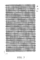
- FIG. 7 is an equivalent circuit of a prior self-capacitance in-cell touch display panel device
- FIG. 8 is an equivalent circuit of the self-capacitance in-cell touch display panel device in accordance with the present invention.
- FIG. 9 is a stacked diagram of the high-sensitivity self-capacitance in-cell touch display panel device in accordance with another embodiment of the present invention.
- FIG. 10 is a stacked diagram of the high-sensitivity self-capacitance in-cell touch display panel device in accordance with still another embodiment of the present invention.
- FIG. 11 is a stacked diagram of the high-sensitivity self-capacitance in-cell touch display panel device in accordance with yet another embodiment of the present invention.
- FIG. 12 is a stacked diagram of the high-sensitivity self-capacitance in-cell touch display panel device in accordance with further another embodiment of the present invention.
- FIG. 13 is a stacked diagram of the high-sensitivity self-capacitance in-cell touch display panel device in accordance with still further another embodiment of the present invention.
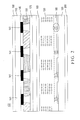
- the high-sensitivity self-capacitance in-cell touch display panel device 100 includes a first substrate 110 , a second substrate 120 , a display material layer 130 , a black matrix layer 140 , a color filter layer 150 , a common voltage (Vcom) layer 160 , a sensing electrode layer 170 , a thin film transistor layer 180 , a first polarizer layer 190 , and a second polarizer layer 200 .
- Vcom common voltage
- the first substrate 110 and the second substrate 120 are preferably glass substrates, and arc parallel to each other.
- the display material layer 130 is disposed between the first and second substrates 110 , 120 .
- the display material layer 130 is preferably a liquid crystal layer.
- the black matrix layer 140 is between the first substrate 110 and the display material layer 130 and is disposed at one side of the first substrate 110 that faces the display material layer 130 .
- the black matrix layer 140 is composed of a plurality of opaque lines 141 arranged in a first direction (X-axis direction) and a second direction (Y-axis direction) for defining a plurality of light-penetrating blocks 143 , wherein the first direction is substantially perpendicular to the second direction.
- FIG. 3 schematically illustrates the black matrix layer 140 , which is the same as that of the prior LCD panel.
- the black matrix layer 140 is composed of a plurality of opaque lines 141 of insulating material that are black and opaque.
- the plurality of lines 141 of black insulating material are arranged as a checkerboard pattern in which the plurality of light-penetrating blocks 143 are defined.
- the plurality of opaque lines 141 are disposed at positions corresponding to those of gate lines and source lines of the thin film transistor layer 180 , wherein the gate lines and source lines are well-known to those skilled in the art of LCD device and thus are not drawn in the figures.
- FIG. 4 is a schematic view of the sensing electrode layer in accordance with the present invention.
- the sensing electrode layer 170 is disposed between the first substrate 110 and the common voltage layer 160 .
- the sensing electrode layer 170 includes a plurality of sensing electrode 171 and a plurality of sensing electrode selection switches 173 . Each sensing electrode selection switch 173 is connected to at least one sensing electrode 171 .
- Each of the sensing electrodes 171 can be a polygon, circle, ellipse, star, wedge shape, radiation shape, triangle, pentagon, hexagon, octagon, rectangle, or square.
- Each sensing electrode 171 is made of material selected from the group consisting of indium tin oxide (ITO), zinc tin oxide thin film, ETO, nano silver, conductive polymer, carbon nanotube, and graphene.
- FIG. 5 schematically illustrates the operation principle of the high-sensitivity self-capacitance in-cell touch display panel device 100 in accordance with the present invention, wherein the grounding of the 5V DC voltage is a first ground (Gdisp) and the grounding of the 9V DC voltage is a second ground (Gtouch). Because the grounding of the 9V DC voltage is the second ground (Gtouch), only 5V can be measured between a node A and the first ground (Gdisp). That is, the 9V DC voltage has no influence to the first ground (Gdisp). Similarly, because the grounding of the 5V DC voltage is the first ground (Gdisp), only 9V can be measured between the node A and the second ground (Gtouch). That is, the 5V DC voltage has no influence to the second ground (Gtouch).
- FIG. 6 is a schematic view of the high-sensitivity self-capacitance in-cell touch display panel device 100 in accordance with the present invention.
- a display control circuit 610 is provided to control the display operation of the self-capacitance in-cell touch display panel device 100 .
- the display control circuit 610 is powered by a first power source (Vccdisp) and is connected to the first ground (Gdisp).
- the display control circuit 610 is connected to the common voltage (Vcom) layer 160 . If the common voltage layer 160 is a DC Vcom layer, the display control circuit 610 electrically connects the first ground (Gdisp) to the common voltage layer 160 . If the common voltage layer 160 is an AC Vcom layer, the display control circuit 610 outputs an AC signal based on the first ground (Gdisp) to the common voltage layer 160 .
- a touch sensing control circuit 620 is connected to the plurality of sensing electrode selection switches 173 for controlling the at least one sensing electrode 171 corresponding to each sensing electrode selection switch 173 so as to perform a touch sensing.
- the touch sensing control circuit 620 is powered by a second power source (Vcctouch) and is connected to the second ground (Gtouch).
- the first power source (Vccdisp) and the first ground (Gdisp) are different from the second power source (Vcctouch) and the second ground (Gtouch); i.e., there is no common current loop therebetween.
- An amplifier 630 with gain greater than zero is connected to the touch sensing control circuit 620 and the common voltage layer 160 .
- the amplifier 630 with gain greater than zero is powered by the second power source (Vcctouch) and is connected to the second ground (Gtouch).
- the touch sensing control circuit 620 applies a sensing signal sensed by a sensing electrode 171 - 1 corresponding to a sensing electrode selection switch 173 - 1 to the amplifier 630 with gain greater than zero for being amplified, so as to generate an in-phase copied sensing signal Vamp for being applied to the common voltage layer 160 , thereby reducing the capacitance effect between the common voltage layer 160 and the sensing electrode 171 - 1 corresponding to the sensing electrode selection switch 173 - 1 .
- the touch sensing control circuit 620 obtains the sensing signal of the sensing electrode 171 - 1 , which is applied to the amplifier 630 with gain greater than zero so as to generate the in-phase copied sensing signal Vamp.
- the in-phase copied sensing signal Vamp is the same as the sensing signal of the sensing electrode 171 - 1 . That is, the sensing electrode 171 - 1 and the common voltage layer 160 have the same voltage level. Because the sensing electrode 171 - 1 and the common voltage layer 160 have the same voltage level, the effective capacitance between the sensing electrode 171 - 1 and the common voltage layer 160 is zero. Therefore, the present invention is able to effectively decrease the capacitance effect between the sensing electrode 171 - 1 and the common voltage layer 160 .
- FIG. 7 is an equivalent circuit of a prior self-capacitance in-cell touch display panel device.
- FIG. 8 is an equivalent circuit of the self-capacitance in-cell touch display panel device in accordance with the present invention for comparison with FIG. 7 .
- the gain of the amplifier 630 with gain greater than zero is preferred to be one.
- the sensing signal on the sensing electrode S is amplified by the amplifier 630 with gain greater than zero for then being applied to the common voltage layer 160 , while the sensing electrode S 1 is not provided with such technique.
- the capacitance between the sensing electrode S and the common voltage layer 160 is zero.
- the capacitance on the sensing electrode S is determined only by the capacitance CFS between the finger and the sensing electrode S and the capacitance CSG between the sensing electrode S and the ground.
- the capacitance on the sensing electrode S 1 is determined by the capacitance CFS 1 between the finger and the sensing electrode S 1 , the capacitance CS 1 G between the sensing electrode S 1 and the ground, the capacitance CS 1 C between the sensing electrode S 1 and the common voltage layer 160 , and the capacitance CCG between the common voltage layer 160 and the ground. From FIG.
- the capacitance CFS between the finger and the sensing electrode S is the major component of the sensing signal, and thus, in comparison with the prior art, the present invention is able to more accurately detect the touch position and also reduce the capacitance effect between the sensing electrode and the common voltage layer 160 .
- the color filter layer 150 is disposed at one side of the black matrix layer 140 that faces the display material layer 130 .
- the thin film transistor layer 180 is disposed at one side of the second substrate 120 that faces the display material layer 130 , and includes K gate lines and L source lines, wherein K, L are each a positive integer, and the gates lines and source lines are well-known to those skilled in the typical LCD device and thus are not shown in the figure.
- the K gate lines are arranged in the first direction
- the L source lines are arranged in the second direction, so as to form a plurality of pixel blocks.
- Each pixel block has a pixel transistor and a capacitor corresponding thereto, so as to drive the corresponding pixel transistor and capacitor according to a display pixel signal and a display driving signal thereby performing, a display operation.
- the plurality of opaque lines 141 are disposed at positions corresponding to those of the K gate lines and L source lines.
- the first polarizer layer 190 is disposed at one side the first substrate 110 opposite to the other side of the first substrate 110 facing the display material layer 130 .
- the second polarizer layer 200 is disposed at one side of the second substrate 120 opposite to the other side of the second substrate 120 facing the display material layer 130 .
- FIG. 9 is a stacked diagram of the high-sensitivity self-capacitance in-cell touch display panel device 900 in accordance with another embodiment of the present invention.
- the high-sensitivity self-capacitance in-cell touch display panel device 900 includes a first substrate 110 , a second substrate 120 , a display material layer 130 , a black matrix layer 140 , a color filter layer 150 , a sensing electrode layer 170 , a thin film transistor layer 180 , a first polarizer layer 190 , and a second polarizer layer 200 .
- This embodiment is similar to that of FIG.
- the sensing electrode layer 170 is disposed at one side of the black matrix layer 140 facing the display material layer 130 and the sensing electrode layer 170 includes a plurality of sensing electrodes, each sensing electrode being formed by metal mesh. That is, the plurality of sensing electrodes 171 are disposed at one side of the black matrix layer 140 facing the display material layer 130 , and the common voltage layer 160 is disposed in the thin film transistor layer 180 .
- the material of the metal mash is selected from the group consisting of chromium, barium, molybdenum, aluminum, silver, copper, titanium, nickel, tantalum, cobalt, tungsten, magnesium (Mg), calcium (Ca), potassium (K), lithium (Li), indium (In), an alloy thereof, fluorine lithium (LiF), magnesium fluoride (MgF 2 ), and lithium oxide (Li 2 O).
- the technique for the sensing electrode 171 formed by metal mesh has been described in detail in US patent Publication No. 20150049264, 20150085208, 20140192275, 20130314371, 20140375911, 20130314371, 20140346493, 20140353691 and 20140326967 filed by the same applicant.
- the common voltage layer 160 being disposed in the thin film transistor layer 180 indicates that the panel is an IPS type LCD panel.
- the black matrix layer 140 is between the first substrate 110 and the display material layer 130 and is disposed at one side of the first substrate 110 that faces the display material layer 130 .
- the black matrix layer 140 is composed of a plurality of opaque lines 141 arranged in a first direction and a second direction for defining a plurality of light-penetrating blocks.
- the color filter layer 150 is disposed at one side of the black matrix layer 140 that faces the display material layer 130 .
- the first polarizer layer 190 is disposed at one side the first substrate 110 opposite to the other side of the first substrate 110 facing the display material layer 130 .
- the thin film transistor layer 180 is disposed at one side of the second substrate 120 that faces the display material layer 130 , and includes K gate lines and L source lines, wherein K, L are each a positive integer, and the gates lines and source lines are well-known to those skilled in the typical LCD device and thus are not shown in the figure.
- K gate lines are arranged in the first direction
- the L source lines are arranged in the second direction, so as to form a plurality of pixel blocks.
- Each pixel block has a pixel transistor and a capacitor corresponding thereto, so as to drive the corresponding pixel transistor and capacitor according to a display pixel signal and a display driving signal thereby performing a display operation.
- the second polarizer layer 200 is disposed at one side of the second substrate 120 opposite to the other side of the second substrate 120 facing the display material layer 130 .
- the plurality of opaque lines 141 are disposed at positions corresponding to those of the K gate lines and L source lines.
- the sensing electrodes formed by metal mesh are disposed at positions corresponding to those of the plurality of opaque lines 141 .
- the sensing electrode layer 170 is disposed in the thin film transistor layer 180 ; i.e., the plurality of sensing electrodes is disposed in the thin film transistor layer 180 .
- the technique for forming metal mesh type sensing electrodes in the thin film transistor layer 180 or forming metal mesh type sensing electrodes on the first substrate 110 has been described in detail in US patent Publication No. 20150049264, 20150085208, 20140192275, 20130314371, 20140375911, 20130314371, 20140346493, 20140353691 and 20140326967 filed by the same applicant.
- FIG. 10 is a stacked diagram of the high-sensitivity self-capacitance in-cell touch display panel device 1000 in accordance with still another embodiment of the present invention.
- the high-sensitivity self-capacitance in-cell touch display panel device 1000 is similar to those of FIG. 2 and FIG. 6 except for the display material layer 930 , the cathode layer 960 , the anode layer 970 and the thin film transistor layer 950 , and the output of the amplifier 630 with gain greater than zero being connected to the cathode layer 960 .
- the touch sensing control circuit 620 applies a sensing signal sensed by at least a sensing electrode corresponding to a sensing electrode selection switch to the amplifier with gain greater than zero for being amplified, so as to generate an in-phase copied sensing signal for being applied to the cathode 960 , thereby reducing the capacitance effect between the cathode layer 960 and the at least one sensing electrode corresponding to the sensing electrode selection switch.
- the display material layer 930 is an organic light emitting diode layer.
- the cathode layer 960 is disposed at one side of the first substrate 110 facing the display material layer 930 and between the first substrate 110 and the display material layer 930 .
- the cathode layer 960 is made of metal material, preferably metal material with thickness being less than 50 nm.
- the metal material is selected from the group consisting of: aluminum (Al), silver (Ag), magnesium (Mg), calcium (Ca), potassium (K), lithium (Li), indium (In), alloy thereof or mixture of lithium fluoride (LiF), magnesium fluoride (MgF 2 ), lithium oxide (Li 2 O) and aluminum.
- the cathode layer 960 Due to the thickness of the cathode layer 960 being less than 50 nm, the light generated by the display material layer 930 can pass through the cathode layer 960 , so as to show images on the first substrate 110 .
- the cathode layer 960 is electrically connected in the whole piece.
- the cathode layer 960 receives the current coming from the anode pixel electrode 971 .
- the color filter layer 150 is disposed at one side of the black matrix layer 140 that faces the display material layer 130 .
- the thin film transistor layer 950 is disposed at one side of the second substrate 120 that faces the display material layer 930 , and includes a plurality of gate lines (not shown), a plurality of source lines (not shown), and a plurality pixel driving circuits 951 .
- Each pixel driving circuit 951 is corresponding to a pixel, so as to drive the corresponding pixel driving circuit 951 according to a display pixel signal and a display driving signal thereby performing a display operation.
- the plurality of gate lines and the plurality c of source lines define a plurality of pixel areas, each corresponding to alight penetrating block 143 .
- driving circuit 95 (such as 2T1C, is formed with two thin film transistors and a storage capacitor, and 6T2C is formed with six thin film transistors and two storage capacitors), a gate 9511 of at least one thin film transistor in the pixel driving circuit 951 is connected to a gate line (not shown).
- driving circuit a source/drain 9513 of at least one thin film transistor in the control circuit is connected to a source line (not shown) and a source/drain 9515 of at least one thin film transistor in pixel driving circuit 951 is connected to a corresponding anode pixel electrode 971 of the anode layer 970 .
- the anode layer 970 is disposed at one site of the thin film transistor layer 950 facing the display material layer 930 and includes a plurality of anode pixel electrodes 971 .
- Each of the anode pixel electrodes 971 is corresponding to one of the pixel driving transistors 951 of the thin film transistor layer 950 . That is, each of the anode pixel electrodes is connected to a source/drain of the corresponding pixel driving transistor 951 , so as to form a pixel electrode of a specific color, for example a red pixel electrode, a green pixel electrode, or a blue pixel electrode.
- the display material layer 930 includes a hole transporting layer 931 an emitting layer 933 , and an electron transporting layer 935 .
- the display material layer 930 preferably generates white light, which is filtered to generate three primary colors of red, blue and green by using the color filter 150 .
- FIG. 11 is a stacked diagram of the high-sensitivity self-capacitance in-cell touch display panel device 1100 in accordance with yet another embodiment of the present invention.
- the high-sensitivity self-capacitance in-cell touch display panel device 1100 is similar to that of FIG. 10 except that: a red emitting layer 933 - 1 , a blue emitting layer 933 - 2 and a green emitting layer 933 - 3 are provided in FIG. 11 so that there is no need to use a color filter layer and a black matrix layer.
- FIG. 12 is a stacked diagram of the high-sensitivity self-capacitance in-cell touch display panel device 1200 in accordance with further another embodiment of the present invention.
- the high-sensitivity self-capacitance in-cell touch display panel device 1200 is similar to that of FIG. 10 except that the positions of the cathode layer 960 and the anode layer 970 are exchanged with each other.
- the cathode layer 960 includes a plurality of cathode pixel electrodes 961 , each corresponding to one pixel driving transistor of the pixel driving circuit 9511 of the thin film transistor layer 950 .
- each of the cathode pixel electrodes is connected to a source/drain 9515 of the pixel driving transistor of the corresponding pixel driving circuit 951 , so as to form a pixel electrode of a specific color, for example a red pixel electrode, a green pixel electrode, or a blue pixel electrode.
- the cathode layer 960 includes a plurality of cathode pixel electrodes 961 . Each of the cathode pixel electrodes 961 is connected to a source/drain of the pixel driving transistor of the corresponding pixel driving circuit.
- the output of the amplifier 630 with gain greater than zero is connected to the anode layer 970 .
- the touch sensing control circuit applies a sensing signal sensed by at least one sensing electrode corresponding to a sensing electrode selection switch to the amplifier with gain greater than zero for being amplified, so as to generate an in-phase copied sensing signal for being applied to the anode 970 , thereby reducing the capacitance effect between the anode layer 970 and the at least one sensing electrode corresponding to the sensing electrode selection switch.
- FIG. 13 is a stacked diagram of the high-sensitivity self-capacitance in-cell touch display panel device 1300 in accordance with still further another embodiment of the present invention.
- the high-sensitivity self-capacitance in-cell touch display panel device 1300 is similar to that of FIG. 12 except that: a red emitting layer 933 - 1 , a blue emitting layer 933 - 2 and a green emitting layer 933 - 3 are provided in FIG. 11 so that there is no need to use a color filter layer and a black matrix layer.
- the sensing signal of a sensing electrode 171 - 1 is amplified by the amplifier 630 with gain greater than zero to generate the in-phase copied sensing signal Vamp, and the in-phase copied sensing signal Vamp is applied to the common voltage layer 160 , so that the sensing electrode 171 - 1 and the common voltage layer 160 have the same voltage level and thus the capacitance between the sensing electrode 171 - 1 and the common voltage layer 160 is zero.
- the capacitance between the finger and sensing electrode is the major component of the sensing signal, and thus, in comparison with the prior art, the present invention is able to more accurately detect the touch position.
- the power source and the ground fir the display control circuit 610 are different from those for the touch sensing control circuit 620 and the amplifier 630 with gain greater than zero, thereby increasing the accuracy in detecting the touch position without interfering with the display quality.
- the sensing electrode layer 170 can be formed in the thin film transistor layer 950 or on one side of the first substrate by metal mesh.
- Such technique has been described in detail in US patent Publication No. 20150049264, 20150085208, 20140192275, 20130314371, 20140375911, 20130314371, 20140346493, 20140353691 and 20140326967 filed by the same applicant.
Landscapes
- Engineering & Computer Science (AREA)
- Physics & Mathematics (AREA)
- Theoretical Computer Science (AREA)
- General Engineering & Computer Science (AREA)
- General Physics & Mathematics (AREA)
- Human Computer Interaction (AREA)
- Nonlinear Science (AREA)
- Crystallography & Structural Chemistry (AREA)
- Chemical & Material Sciences (AREA)
- Optics & Photonics (AREA)
- Mathematical Physics (AREA)
- Computer Hardware Design (AREA)
- Position Input By Displaying (AREA)
- Liquid Crystal (AREA)
Abstract
A high-sensitivity self-capacitance in-cell touch display panel device includes a sensing electrode layer having plural sensing electrodes, a display control circuit, a touch sensing control circuit, and an amplifier with gain greater than zero. The display control circuit is powered by a first power source and connected to a first ground. The touch sensing control circuit is coupled to the sensing electrodes for performing a touch sensing. The touch sensing control circuit is powered by a second power source and connected to a second ground, wherein the first power source and the first ground are different from the second power source and the second ground. The amplifier is connected to the touch sensing control circuit and a common voltage layer. The touch sensing control circuit applies a sensing signal sensed by at least one sensing electrode to the amplifier for being amplified and applied to the common voltage layer.
Description
1. Field of the Invention
The present invention relates to the technical field of touch panels and, more particularly, to a high-sensitivity self-capacitance in-cell touch display panel device.
2. Description of Related Art
The conventional touch display panel includes a touch panel and a display unit overlapped with the touch panel. The touch panel is configured as an operation interface. The touch panel is transparent so that an image generated by the display unit can be viewed directly by a user without being sheltered by the touch panel. Such well known skill of the touch panel may increase additional weight and thickness of the touch display panel, and may further reduce the light penetration rate, and increase reflectance and haze of the touch display panel.
On-cell and in-cell touch technology were invented to overcome the drawbacks of traditional touch technology described above. The on-cell technology is to dispose a sensor on the back side of a color filter substrate to form a completed color filter substrate. One of the on-cell touch technologies is provided to dispose a touch sensor on a thin film and then bond the thin film onto the upper one of the two substrates. The in-cell technology is to dispose the sensor within the LCD cell structure. However, when the sensor is disposed within the LCD cell structure, the distance between the sensor and the common voltage layer is only several micro meters and thus the capacitance induced therebetween is greatly increased, such that, in comparison with such a large capacitance, the capacitance change caused by touch is too small to be detected. Furthermore, because of the short distance, the display signal may be seriously interfered, resulting in a had display quality.
The object of the present invention is to provide a high-sensitivity self-capacitance in-cell touch display panel device, which can effectively reduce the capacitance effect generated between the sensing electrode and the common voltage layer without interfering the display signal, so that the touch sensing and the display driving are not required to operate in a time-sharing manner. Therefore, the size of the in-cell touch panel is no longer restricted and the sensing and production difficulty is lowered, so as to not only easily and accurately detect the finger's touch but also reduce the manufacturing cost.
In one aspect of the present invention, there is provided high-sensitivity self-capacitance touch display panel device, which comprises: a first substrate; a second substrate parallel to the first substrate; a display material layer configured between the first substrate and the second substrate; to common voltage layer disposed between the first substrate and the display material layer; a sensing electrode layer disposed between the first substrate and the common voltage layer, and having plurality of sensing electrodes; a plurality of sensing electrode selection switches, each corresponding to at least one sensing electrode; a display control circuit for controlling the high-sensitivity self-capacitance in-cell touch display panel device to display image, wherein the display control circuit is powered by a first power source and is connected to a first ground; a touch sensing control circuit connected to the plurality of sensing electrode selection switches for controlling the at least one sensing electrode corresponding to each sensing electrode selection switch so as to perform a touch sensing, wherein the touch sensing control circuit is powered by a second power source and is connected to a second ground; and an amplifier with gain greater than zero connected to the touch sensing control circuit and the common voltage layer, wherein the first power source and the first ground are different from the second power source and the second ground and, in detection, the touch sensing control circuit applies a sensing signal sensed by the at least one sensing electrode corresponding to a sensing electrode selection switch to the amplifier with gain greater than zero for being amplified so as to generate an in-phase copied sensing signal that is applied to the common voltage layer, thereby reducing the capacitance effect between the common voltage layer and the at least one sensing electrode corresponding to the sensing electrode selection switch.
In another aspect of the present invention, there is provided a high-sensitivity self-capacitance in-cell touch display panel device, which comprises: a first substrate; a common voltage layer; a second substrate parallel to the first substrate; a display material layer configured between the first substrate and the second substrate; a plurality of sensing electrodes, each formed by metal mesh; a plurality of sensing electrode selection switches, each corresponding to at least one sensing electrode; a display control circuit for controlling the high-sensitivity self-capacitance in-cell touch display panel device to display image, wherein the display control circuit is powered by a first power source and is connected to a first ground; a touch sensing control circuit connected to the plurality of sensing electrode selection switches for controlling the at least one sensing electrode corresponding to each sensing electrode selection switch so as to perform a touch sensing, wherein the touch sensing control circuit is powered by a second power source and is connected to a second ground; and an amplifier with gain greater than zero connected to the touch sensing control circuit and the common voltage layer, wherein the first power source and the first ground are different from the second power source and the second ground and, in detection, the touch sensing control circuit applies a sensing signal sensed by the at least one sensing electrode corresponding to a sensing electrode selection switch to the amplifier with gain greater than zero for being amplified so as to generate an in-phase copied sensing signal that is applied to the common voltage layer, thereby reducing the capacitance effect between the common voltage layer and the at least one sensing electrode corresponding to the sensing electrode selection switch.
In still another aspect of the present invention, there is provided a high-sensitivity self-capacitance in-cell touch display panel device, which comprises: a first substrate; a second substrate parallel to the first substrate; a display material layer configured between the first substrate and the second substrate; a cathode layer disposed at one side of the first substrate facing the display material layer; a sensing electrode layer disposed between the first substrate and the second substrate, and having a plurality of sensing electrodes; a plurality of sensing electrode selection switches, each corresponding to at least one sensing electrode; a display control circuit for controlling the high-sensitivity self-capacitance in-cell touch display panel device to display image, wherein the display control circuit is powered by a first power source and is connected to a first ground; a touch sensing control circuit connected to the plurality of sensing electrode selection switches for controlling the at least one sensing electrode corresponding to each sensing electrode selection switch so as to perform a touch sensing, wherein the touch sensing control circuit is powered by a second power source and is connected to a second ground; and an amplifier with gain greater than zero connected to the touch sensing control circuit and the cathode layer, wherein the first power source and the first ground are different from the second power source and the second ground and, in detection, the touch sensing control circuit applies a sensing signal sensed by the at least one sensing electrode corresponding to a sensing electrode selection switch to the amplifier with gain greater than zero for being amplified so as to generate an in-phase copied sensing signal that is applied to the cathode layer, thereby reducing the capacitance effect between the cathode layer and the at least one sensing electrode corresponding to the sensing electrode selection switch.
In yet another aspect of the present invention, there is provided a high-sensitivity self-capacitance in-cell touch display panel device, which comprises: a first substrate; a second substrate parallel to the first substrate; a display material layer configured between the first substrate and the second substrate; an anode layer disposed at one side of the first substrate facing the display material; a sensing; electrode layer disposed between the first substrate and the second substrate, and having a plurality of sensing electrodes; a plurality of sensing electrode selection switches, each corresponding to at least one sensing electrode; a display control circuit for controlling the high-sensitivity self-capacitance in-cell touch display panel device to display image, wherein the display control circuit is powered by a first power source and is connected to a first ground; a touch sensing control circuit connected to the plurality of sensing electrode selection switches for controlling the at least one sensing electrode corresponding to each sensing electrode selection switch so as to perform a touch sensing, wherein the touch sensing control circuit is powered by a second power source and is connected to a second ground and an amplifier with gain greater than zero connected to the touch sensing control circuit and the anode layer, wherein the first power source and the first ground are different from the second power source and the second ground and, in detection, the touch sensing control circuit applies a sensing signal sensed by the at least one sensing electrode corresponding to a sensing electrode selection switch to the amplifier with gain greater than zero for being amplified so as to generate an in-phase copied sensing signal that is applied to the anode layer, thereby reducing the capacitance effect between the anode layer and the at least one sensing electrode corresponding to the sensing electrode selection switch.
Other objects, advantages, and novel features of the invention will become more apparent from the following detailed description when taken in conjunction with the accompanying drawings.
With reference to FIG. 2 , there is shown a high-sensitivity self-capacitance in-cell touch display panel device in accordance with one embodiment of the present invention. As shown, the high-sensitivity self-capacitance in-cell touch display panel device 100 includes a first substrate 110, a second substrate 120, a display material layer 130, a black matrix layer 140, a color filter layer 150, a common voltage (Vcom) layer 160, a sensing electrode layer 170, a thin film transistor layer 180, a first polarizer layer 190, and a second polarizer layer 200.
The first substrate 110 and the second substrate 120 are preferably glass substrates, and arc parallel to each other. The display material layer 130 is disposed between the first and second substrates 110, 120. In this embodiment, the display material layer 130 is preferably a liquid crystal layer.
The black matrix layer 140 is between the first substrate 110 and the display material layer 130 and is disposed at one side of the first substrate 110 that faces the display material layer 130. As shown in FIG. 3 , the black matrix layer 140 is composed of a plurality of opaque lines 141 arranged in a first direction (X-axis direction) and a second direction (Y-axis direction) for defining a plurality of light-penetrating blocks 143, wherein the first direction is substantially perpendicular to the second direction.
Each of the sensing electrodes 171 can be a polygon, circle, ellipse, star, wedge shape, radiation shape, triangle, pentagon, hexagon, octagon, rectangle, or square. Each sensing electrode 171 is made of material selected from the group consisting of indium tin oxide (ITO), zinc tin oxide thin film, ETO, nano silver, conductive polymer, carbon nanotube, and graphene.
With reference to both FIG. 4 and FIG. 6 , a touch sensing control circuit 620 is connected to the plurality of sensing electrode selection switches 173 for controlling the at least one sensing electrode 171 corresponding to each sensing electrode selection switch 173 so as to perform a touch sensing. The touch sensing control circuit 620 is powered by a second power source (Vcctouch) and is connected to the second ground (Gtouch). The first power source (Vccdisp) and the first ground (Gdisp) are different from the second power source (Vcctouch) and the second ground (Gtouch); i.e., there is no common current loop therebetween.
An amplifier 630 with gain greater than zero is connected to the touch sensing control circuit 620 and the common voltage layer 160. The amplifier 630 with gain greater than zero is powered by the second power source (Vcctouch) and is connected to the second ground (Gtouch). In performing a touching sensing detection, the touch sensing control circuit 620 applies a sensing signal sensed by a sensing electrode 171-1 corresponding to a sensing electrode selection switch 173-1 to the amplifier 630 with gain greater than zero for being amplified, so as to generate an in-phase copied sensing signal Vamp for being applied to the common voltage layer 160, thereby reducing the capacitance effect between the common voltage layer 160 and the sensing electrode 171-1 corresponding to the sensing electrode selection switch 173-1.
In case that the amplification factor of the amplifier 630 with gain greater than zero is one, the touch sensing control circuit 620 obtains the sensing signal of the sensing electrode 171-1, which is applied to the amplifier 630 with gain greater than zero so as to generate the in-phase copied sensing signal Vamp. The in-phase copied sensing signal Vamp is the same as the sensing signal of the sensing electrode 171-1. That is, the sensing electrode 171-1 and the common voltage layer 160 have the same voltage level. Because the sensing electrode 171-1 and the common voltage layer 160 have the same voltage level, the effective capacitance between the sensing electrode 171-1 and the common voltage layer 160 is zero. Therefore, the present invention is able to effectively decrease the capacitance effect between the sensing electrode 171-1 and the common voltage layer 160.
When a finger comes into touch with the sensing electrode S and the sensing electrode S1, the capacitance between the sensing electrode S and the common voltage layer 160 is zero. The capacitance on the sensing electrode S is determined only by the capacitance CFS between the finger and the sensing electrode S and the capacitance CSG between the sensing electrode S and the ground. The capacitance on the sensing electrode S1 is determined by the capacitance CFS1 between the finger and the sensing electrode S1, the capacitance CS1G between the sensing electrode S1 and the ground, the capacitance CS1C between the sensing electrode S1 and the common voltage layer 160, and the capacitance CCG between the common voltage layer 160 and the ground. From FIG. 8 , it is known that the capacitance CFS between the finger and the sensing electrode S is the major component of the sensing signal, and thus, in comparison with the prior art, the present invention is able to more accurately detect the touch position and also reduce the capacitance effect between the sensing electrode and the common voltage layer 160.
With reference to FIG. 2 again, the color filter layer 150 is disposed at one side of the black matrix layer 140 that faces the display material layer 130.
The thin film transistor layer 180 is disposed at one side of the second substrate 120 that faces the display material layer 130, and includes K gate lines and L source lines, wherein K, L are each a positive integer, and the gates lines and source lines are well-known to those skilled in the typical LCD device and thus are not shown in the figure. The K gate lines are arranged in the first direction, and the L source lines are arranged in the second direction, so as to form a plurality of pixel blocks. Each pixel block has a pixel transistor and a capacitor corresponding thereto, so as to drive the corresponding pixel transistor and capacitor according to a display pixel signal and a display driving signal thereby performing, a display operation. The plurality of opaque lines 141 are disposed at positions corresponding to those of the K gate lines and L source lines.
The first polarizer layer 190 is disposed at one side the first substrate 110 opposite to the other side of the first substrate 110 facing the display material layer 130. The second polarizer layer 200 is disposed at one side of the second substrate 120 opposite to the other side of the second substrate 120 facing the display material layer 130.
The technique for the sensing electrode 171 formed by metal mesh has been described in detail in US patent Publication No. 20150049264, 20150085208, 20140192275, 20130314371, 20140375911, 20130314371, 20140346493, 20140353691 and 20140326967 filed by the same applicant. The common voltage layer 160 being disposed in the thin film transistor layer 180 indicates that the panel is an IPS type LCD panel.
The black matrix layer 140 is between the first substrate 110 and the display material layer 130 and is disposed at one side of the first substrate 110 that faces the display material layer 130. The black matrix layer 140 is composed of a plurality of opaque lines 141 arranged in a first direction and a second direction for defining a plurality of light-penetrating blocks.
The color filter layer 150 is disposed at one side of the black matrix layer 140 that faces the display material layer 130. The first polarizer layer 190 is disposed at one side the first substrate 110 opposite to the other side of the first substrate 110 facing the display material layer 130. The thin film transistor layer 180 is disposed at one side of the second substrate 120 that faces the display material layer 130, and includes K gate lines and L source lines, wherein K, L are each a positive integer, and the gates lines and source lines are well-known to those skilled in the typical LCD device and thus are not shown in the figure. The K gate lines are arranged in the first direction, and the L source lines are arranged in the second direction, so as to form a plurality of pixel blocks. Each pixel block has a pixel transistor and a capacitor corresponding thereto, so as to drive the corresponding pixel transistor and capacitor according to a display pixel signal and a display driving signal thereby performing a display operation. The second polarizer layer 200 is disposed at one side of the second substrate 120 opposite to the other side of the second substrate 120 facing the display material layer 130.
The plurality of opaque lines 141 are disposed at positions corresponding to those of the K gate lines and L source lines. The sensing electrodes formed by metal mesh are disposed at positions corresponding to those of the plurality of opaque lines 141.
In other embodiments, the sensing electrode layer 170 is disposed in the thin film transistor layer 180; i.e., the plurality of sensing electrodes is disposed in the thin film transistor layer 180. The technique for forming metal mesh type sensing electrodes in the thin film transistor layer 180 or forming metal mesh type sensing electrodes on the first substrate 110 has been described in detail in US patent Publication No. 20150049264, 20150085208, 20140192275, 20130314371, 20140375911, 20130314371, 20140346493, 20140353691 and 20140326967 filed by the same applicant.
The cathode layer 960 is disposed at one side of the first substrate 110 facing the display material layer 930 and between the first substrate 110 and the display material layer 930. The cathode layer 960 is made of metal material, preferably metal material with thickness being less than 50 nm. The metal material is selected from the group consisting of: aluminum (Al), silver (Ag), magnesium (Mg), calcium (Ca), potassium (K), lithium (Li), indium (In), alloy thereof or mixture of lithium fluoride (LiF), magnesium fluoride (MgF2), lithium oxide (Li2O) and aluminum. Due to the thickness of the cathode layer 960 being less than 50 nm, the light generated by the display material layer 930 can pass through the cathode layer 960, so as to show images on the first substrate 110. The cathode layer 960 is electrically connected in the whole piece. The cathode layer 960 receives the current coming from the anode pixel electrode 971.
The color filter layer 150 is disposed at one side of the black matrix layer 140 that faces the display material layer 130.
The thin film transistor layer 950 is disposed at one side of the second substrate 120 that faces the display material layer 930, and includes a plurality of gate lines (not shown), a plurality of source lines (not shown), and a plurality pixel driving circuits 951. Each pixel driving circuit 951 is corresponding to a pixel, so as to drive the corresponding pixel driving circuit 951 according to a display pixel signal and a display driving signal thereby performing a display operation. The plurality of gate lines and the plurality c of source lines define a plurality of pixel areas, each corresponding to alight penetrating block 143.
According to different designs of driving circuit 95 (such as 2T1C, is formed with two thin film transistors and a storage capacitor, and 6T2C is formed with six thin film transistors and two storage capacitors), a gate 9511 of at least one thin film transistor in the pixel driving circuit 951 is connected to a gate line (not shown). According to different designs of driving circuit, a source/drain 9513 of at least one thin film transistor in the control circuit is connected to a source line (not shown) and a source/drain 9515 of at least one thin film transistor in pixel driving circuit 951 is connected to a corresponding anode pixel electrode 971 of the anode layer 970.
The anode layer 970 is disposed at one site of the thin film transistor layer 950 facing the display material layer 930 and includes a plurality of anode pixel electrodes 971. Each of the anode pixel electrodes 971 is corresponding to one of the pixel driving transistors 951 of the thin film transistor layer 950. That is, each of the anode pixel electrodes is connected to a source/drain of the corresponding pixel driving transistor 951, so as to form a pixel electrode of a specific color, for example a red pixel electrode, a green pixel electrode, or a blue pixel electrode.
The display material layer 930 includes a hole transporting layer 931 an emitting layer 933, and an electron transporting layer 935. The display material layer 930 preferably generates white light, which is filtered to generate three primary colors of red, blue and green by using the color filter 150.
In FIG. 12 , corresponding to the exchange of the positions of the cathode layer 960 and the anode layer 970, the positions of the hole transporting layer 931 and the electron transporting layer 935 of the display material layer 930 are also exchanged with each other. The cathode layer 960 includes a plurality of cathode pixel electrodes 961. Each of the cathode pixel electrodes 961 is connected to a source/drain of the pixel driving transistor of the corresponding pixel driving circuit.
In this embodiment, the output of the amplifier 630 with gain greater than zero is connected to the anode layer 970. In performing a touch sensing detection, the touch sensing control circuit applies a sensing signal sensed by at least one sensing electrode corresponding to a sensing electrode selection switch to the amplifier with gain greater than zero for being amplified, so as to generate an in-phase copied sensing signal for being applied to the anode 970, thereby reducing the capacitance effect between the anode layer 970 and the at least one sensing electrode corresponding to the sensing electrode selection switch.
In view of the foregoing, it is known that, in detecting a finger's touch, the sensing signal of a sensing electrode 171-1 is amplified by the amplifier 630 with gain greater than zero to generate the in-phase copied sensing signal Vamp, and the in-phase copied sensing signal Vamp is applied to the common voltage layer 160, so that the sensing electrode 171-1 and the common voltage layer 160 have the same voltage level and thus the capacitance between the sensing electrode 171-1 and the common voltage layer 160 is zero. The capacitance between the finger and sensing electrode is the major component of the sensing signal, and thus, in comparison with the prior art, the present invention is able to more accurately detect the touch position. Furthermore, in order to prevent the display panel from being interfered by the in-phase copied sensing signal Vamp applied to the common voltage layer 160, the power source and the ground fir the display control circuit 610 are different from those for the touch sensing control circuit 620 and the amplifier 630 with gain greater than zero, thereby increasing the accuracy in detecting the touch position without interfering with the display quality.
In other embodiments, the sensing electrode layer 170 can be formed in the thin film transistor layer 950 or on one side of the first substrate by metal mesh. Such technique has been described in detail in US patent Publication No. 20150049264, 20150085208, 20140192275, 20130314371, 20140375911, 20130314371, 20140346493, 20140353691 and 20140326967 filed by the same applicant.
Although the present invention has been explained in relation to its preferred embodiment, it is to be understood that man other possible modifications and variations can be made without departing from the spirit and scope of the invention as hereinafter claimed.
Claims (29)
1. A high-sensitivity self-capacitance in-cell touch display panel device, comprising:
a first substrate;
a second substrate parallel to the first substrate;
a display material layer configured between the first substrate and the second substrate;
a common voltage layer disposed between the first substrate and the display material layer;
a sensing electrode layer disposed between the first substrate and the common voltage layer, and having a plurality of sensing electrodes;
a plurality of sensing electrode selection switches, each corresponding to exactly one of the sensing electrodes;
a display control circuit for controlling the high-sensitivity self-capacitance in-cell touch display panel device to display an image wherein the display control circuit is powered by a first power source and is connected to a first ground;
a touch sensing control circuit connected to the plurality of sensing electrode selection switches for controlling each of the sensing electrodes to perform a self-capacitance touch sensing, wherein the touch sensing control circuit is powered by a second power source and is connected to a second ground; and
an amplifier with gain greater than zero connected to the touch sensing control circuit and the common voltage layer, wherein the first power source and the first ground are different from the second power source and the second ground, and
wherein in detection of a touch position a sensing signal from a sensing electrode of the plurality of sensing electrodes is applied to the common voltage layer through the amplifier by the touch sensing control circuit so as to reduce a capacitance between the sensing electrode and the common voltage layer.
2. The high-sensitivity self-capacitance in-cell touch display panel device as claimed in claim 1 , further comprising:
a black matrix layer disposed at one side of the first substrate facing the display material layer, the black matrix layer being composed of a plurality of opaque lines arranged in a first direction and a second direction thereby defining a plurality of light-penetrating blocks, wherein the first direction is perpendicular to the second direction;
a color filter layer disposed at one side of black matrix layer facing the display material layer;
a first polarizer layer disposed at one side the first substrate opposite to the other side of the first substrate facing the display material layer;
a thin film transistor layer disposed at the side of the second substrate facing the display material layer, and including K gate lines and L source lines, where K and L are each a positive integer, the K gate lines being arranged in the first direction and the L source lines being arranged in the second direction for forming a plurality of pixel blocks, each pixel block having a pixel transistor and a capacitor corresponding thereto, so as to drive the corresponding pixel transistor and capacitor according to a display pixel signal and a display driving signal thereby performing a display operation; and
a second polarizer layer disposed at one side of the second substrate opposite to the other side of the second substrate facing the display material layer,
wherein the plurality of opaque lines is disposed at positions corresponding to those of the K gate lines and L source lines.
3. The high-sensitivity self-capacitance in-cell touch display panel device as claimed in claim 2 , wherein each of the sensing electrodes is a polygon, circle, ellipse, star, wedge shape, radiation shape, triangle, pentagon, hexagon, octagon, rectangle, or square.
4. The high-sensitivity self-capacitance in-cell touch display panel device as claimed in claim 3 , wherein each of the sensing electrodes is made of material selected from the group consisting of indium tin oxide, zinc tin oxide thin film, ETO, nano silver, conductive polymer, carbon nanotube, and graphene.
5. A high-sensitivity self-capacitance in-cell touch display panel device, comprising:
a first substrate;
a common voltage layer;
a second substrate parallel to the first substrate;
a display material layer configured between the first substrate and the second substrate;
a plurality of sensing electrodes, each formed by metal mesh;
a plurality of sensing electrode selection switches, each corresponding to exactly one of the sensing electrodes;
a display control circuit for controlling the high-sensitivity self-capacitance in-cell touch display panel device to display an image, wherein the display control circuit is powered by a first power source and is connected to a first ground;
a touch sensing control circuit connected to the plurality of sensing electrode selection switches for controlling each of the sensing electrodes to perform a self-capacitance touch sensing, wherein the touch sensing control circuit is powered by a second power source and is connected to a second ground; and
an amplifier with gain greater than zero connected to the touch sensing control circuit and the common voltage layer,
wherein the first power source and the first ground are different from the second power source and the second ground, and
in detection of a touch position, a sensing signal from a sensing electrode of the plurality of sensing electrodes is applied to the common voltage layer through the amplifier by the touch sensing control circuit so as to reduce a capacitance between the sensing electrode and the common voltage layer.
6. The high-sensitivity self-capacitance in-cell touch display panel device as claimed in claim 5 , further comprising:
a black matrix layer disposed at one side of the first substrate facing the display material layer, the black matrix layer being composed of a plurality of opaque lines arranged in a first direction and a second direction thereby defining a plurality of light-penetrating blocks, wherein the first direction is perpendicular to the second direction;
a color filter layer disposed at one side of black matrix layer facing the display material layer;
a first polarizer layer disposed at one side the first substrate opposite to the other side of the first substrate facing the display material layer;
a thin film transistor layer disposed at the side of the second substrate facing the display material layer, and including K gate lines and L source lines, where K and L are each a positive integer, the K gate lines being arranged in the first direction and the L source lines being arranged in the second direction for forming a plurality of pixel blocks, each pixel block having a pixel transistor and a capacitor corresponding thereto, so as to drive the corresponding pixel transistor and capacitor according to a display pixel signal and a display driving signal thereby performing a display operation; and
a second polarizer layer disposed at one side of the second substrate opposite to the other side of the second substrate facing the display material layer.
7. The high-sensitivity self-capacitance in-cell touch display panel device as claimed in claim 6 , wherein the plurality of opaque lines is disposed at positions corresponding to those of the K gate lines and L source lines.
8. The high-sensitivity self-capacitance in-cell touch display panel device as claimed in claim 7 , wherein each sensing electrode formed by metal mesh is a polygon, circle, ellipse, star, wedge shape, radiation shape, triangle, pentagon, hexagon, octagon, rectangle, or square.
9. The high-sensitivity self-capacitance in-cell touch display panel device as claimed in claim 8 , wherein each sensing electrode formed by metal mesh is made of material selected from the group consisting of chromium, barium, molybdenum, aluminum, silver, copper, titanium, nickel, tantalum, cobalt, tungsten, magnesium, calcium, potassium, lithium, indium, an alloy thereof, fluorine lithium, magnesium fluoride, and lithium oxide.
10. The high-sensitivity self-capacitance in-cell touch display panel device as claimed in claim 9 , wherein the plurality of sensing electrodes is disposed at one side of the black matrix layer facing the display material layer.
11. The high-sensitivity self-capacitance in-cell touch display panel device as claimed in claim 9 , wherein the plurality of sensing electrodes is disposed in the thin film transistor layer.
12. A high-sensitivity self-capacitance in-cell touch display panel device, comprising:
a first substrate;
a second substrate parallel to the first substrate;
a display material layer configured between the first substrate and the second substrate;
a cathode layer disposed at one side of the first substrate facing the display material;
a sensing electrode layer disposed between the first substrate and the second substrate, and having a plurality of sensing electrodes;
a plurality of sensing electrode selection switches, each corresponding to exactly one of the sensing electrodes;
a display control circuit for controlling the high-sensitivity self-capacitance in-cell touch display panel device to display an image, wherein the display control circuit is powered by a first power source and is connected to a first ground;
a touch sensing control circuit connected to the plurality of sensing electrode selection switches for controlling each of the sensing electrodes to perform a self-capacitance touch sensing, wherein the touch sensing control circuit is powered by a second power source and is connected to a second ground; and
an amplifier with gain greater than zero connected to the touch sensing control circuit and the cathode layer,
wherein the first power source and the first ground are different from the second power source and the second ground, and
in detection of a touch position, a sensing signal from a sensing electrode of the plurality of sensing electrodes is applied to the cathode layer through the amplifier by the touch sensing control circuit so as to reduce a capacitance between the sensing electrode and the cathode layer.
13. The high-sensitivity self-capacitance in-cell touch display panel device as claimed in claim 12 , further comprising:
a thin film transistor layer disposed at one side of the second substrate facing the display material layer, and including K gate lines and L source lines, where K and L are each a positive integer, the K gate lines being arranged in a first direction and the L source lines being arranged in a second direction for forming a plurality of pixel blocks, each pixel block having a pixel transistor and a capacitor corresponding thereto, so as to drive the corresponding pixel transistor and capacitor according to a display pixel signal and a display driving signal thereby performing a display operation, wherein the first direction is perpendicular to the second direction.
14. The high-sensitivity self-capacitance in-cell touch display panel device as claimed in claim 13 , further comprising:
a black matrix layer disposed at one side of the first substrate facing the display material layer, the black matrix layer being composed of a plurality of opaque lines arranged in the first direction and the second direction thereby defining a plurality of light-penetrating blocks; and
a color filter layer disposed at one side of black matrix layer facing the display material layer,
wherein the plurality of opaque lines is disposed at positions corresponding to those of the K gate lines and L source lines.
15. The high-sensitivity self-capacitance in-cell touch display panel device as claimed in claim 13 , wherein each of the sensing electrodes is a polygon, circle, ellipse, star, wedge shape, radiation shape, triangle, pentagon, hexagon, octagon, rectangle, or square.
16. The high-sensitivity self-capacitance in-cell touch display panel device as claimed in claim 15 , wherein each of the sensing electrodes is made of material selected from the group consisting of indium tin oxide, zinc tin oxide thin film, ETO, nano silver, conductive polymer, carbon nanotube, and graphene.
17. The high-sensitivity self-capacitance in-cell touch display panel device as claimed in claim 15 , wherein each sensing electrode is formed by metal mesh.
18. The high-sensitivity self-capacitance in-cell touch display panel device as claimed in claim 17 , wherein each sensing electrode formed by metal mesh is made of material selected from the group consisting of chromium, barium, molybdenum, aluminum, silver, copper, titanium, nickel, tantalum, cobalt, tungsten, magnesium, calcium, potassium, lithium, indium, an alloy thereof, fluorine lithium, magnesium fluoride, and lithium oxide.
19. The high-sensitivity self-capacitance in-cell touch display panel device as claimed in claim 18 , wherein the plurality of sensing electrodes is disposed at one side of the black matrix layer facing the display material layer.
20. The high-sensitivity self-capacitance in-cell touch display panel device as claimed in claim 18 , wherein the plurality of sensing electrodes is disposed in the thin film transistor layer.
21. A high-sensitivity self-capacitance in-cell touch display panel device, comprising:
a first substrate;
a second substrate parallel to the first substrate;
a display material layer configured between the first substrate and the second substrate; an anode layer disposed at one side of the first substrate facing the display material;
a sensing electrode layer disposed between the first substrate and the second substrate, and having a plurality of sensing electrodes;
a plurality of sensing electrode selection switches, each corresponding to exactly one of the sensing electrodes;
a display control circuit for controlling the high-sensitivity self-capacitance in-cell touch display panel device to display an image, wherein the display control circuit is powered by a first power source and is connected to a first ground;
a touch sensing control circuit connected to the plurality of sensing electrode selection switches for controlling each of the sensing electrodes to perform a self-capacitance touch sensing, wherein the touch sensing control circuit is powered by a second power source and is connected to a second ground; and
an amplifier with gain greater than zero connected to the touch sensing control circuit and the anode layer,
wherein the first power source and the first ground are different from the second power source and the second ground, and
in detection of a touch position a sensing signal from a sensing electrode of the plurality of sensing electrodes is applied to the anode layer through the amplifier by the touch sensing control circuit so as to reduce a capacitance between the sensing electrode and the anode layer.
22. The high-sensitivity self-capacitance in-cell touch display panel device as claimed in claim 21 , further comprising:
a thin film transistor layer disposed at one side of the second substrate facing the display material layer, and including K gate lines and L source lines, where K and L are each a positive integer, the K gate lines being arranged in a first direction and the L source lines being arranged in a second direction for forming a plurality of pixel blocks, each pixel block having a pixel transistor and a capacitor corresponding thereto, so as to drive the corresponding pixel transistor and capacitor according to a display pixel signal and a display driving signal thereby performing a display operation, wherein the first direction is perpendicular to the second direction.
23. The high-sensitivity self-capacitance in-cell touch display panel device as claimed in claim 22 , further comprising:
a black matrix layer disposed at one side of the first substrate facing the display material layer, the black matrix layer being composed of a plurality of opaque lines arranged in the first direction and the second direction thereby defining a plurality of light-penetrating blocks; and
a color filter layer disposed at one side of black matrix layer facing the display material layer,
wherein the plurality of opaque lines is disposed at positions corresponding to those of the K gate lines and L source lines.
24. The high-sensitivity self-capacitance in-cell touch display panel device as claimed in claim 22 , wherein each of the sensing electrodes is a polygon, circle, ellipse, star, wedge shape, radiation shape, triangle, pentagon, hexagon, octagon, rectangle, or square.
25. The high-sensitivity self-capacitance in-cell touch display panel device as claimed in claim 24 , wherein each of the sensing electrodes is made of material selected from the group consisting of indium tin oxide, zinc tin oxide thin film, ETO, nano silver, conductive polymer, carbon nanotube, and graphene.
26. The high-sensitivity self-capacitance in-cell touch display panel device as claimed in claim 24 , wherein each sensing electrode is formed by metal mesh.
27. The high-sensitivity self-capacitance in-cell touch display panel device as claimed in claim 26 , wherein each sensing electrode formed by metal mesh is made of material selected from the group consisting of chromium, barium, molybdenum, aluminum, silver, copper, titanium, nickel, tantalum, cobalt, tungsten, magnesium, calcium, potassium, lithium, indium, an alloy thereof, fluorine lithium, magnesium fluoride, and lithium oxide.
28. The high-sensitivity self-capacitance in-cell touch display panel device as claimed in claim 27 , wherein the plurality of sensing electrodes is disposed at one side of the black matrix layer facing the display material layer.
29. The high-sensitivity self-capacitance in-cell touch display panel device as claimed in claim 27 , wherein the plurality of sensing electrodes is disposed in the thin film transistor layer.
Applications Claiming Priority (3)
| Application Number | Priority Date | Filing Date | Title |
|---|---|---|---|
| TW103138723A | 2014-11-07 | ||
| TW103138723A TWI546586B (en) | 2014-11-07 | 2014-11-07 | High-sensitivity self-capacitance in-cell touch display panel device |
| TW103138723 | 2014-11-07 |
Publications (2)
| Publication Number | Publication Date |
|---|---|
| US20160132154A1 US20160132154A1 (en) | 2016-05-12 |
| US9965119B2 true US9965119B2 (en) | 2018-05-08 |
Family
ID=55740789
Family Applications (1)
| Application Number | Title | Priority Date | Filing Date |
|---|---|---|---|
| US14/932,496 Active 2036-01-04 US9965119B2 (en) | 2014-11-07 | 2015-11-04 | High-sensitivity self-capacitance in-cell touch display panel device |
Country Status (3)
| Country | Link |
|---|---|
| US (1) | US9965119B2 (en) |
| CN (1) | CN205176820U (en) |
| TW (1) | TWI546586B (en) |
Cited By (4)
| Publication number | Priority date | Publication date | Assignee | Title |
|---|---|---|---|---|
| US10268297B2 (en) * | 2017-05-07 | 2019-04-23 | Superc-Touch Corporation | Mutual-capacitance organic light emitting touch display apparatus |
| US10268298B2 (en) * | 2017-05-07 | 2019-04-23 | Superc-Touch Corporation | Mutual-capacitance touch apparatus and highly sensitive mutual-capacitance touch sensing method for the same |
| US10545620B1 (en) * | 2018-07-19 | 2020-01-28 | Superc-Touch Corporation | Hovering and touch sensing apparatus with auxiliary capacitance-exciting signal |
| US11068087B2 (en) | 2016-09-09 | 2021-07-20 | Samsung Display Co., Ltd. | Electronic device |
Families Citing this family (20)
| Publication number | Priority date | Publication date | Assignee | Title |
|---|---|---|---|---|
| JP5366051B2 (en) | 2009-04-20 | 2013-12-11 | 株式会社ジャパンディスプレイ | Information input device, display device |
| US10001876B2 (en) * | 2015-04-01 | 2018-06-19 | Shanghai Tianma Micro-electronics Co., Ltd. | Touch display panel, and driving method and driving circuit for the same |
| CN104898911A (en) * | 2015-06-17 | 2015-09-09 | 京东方科技集团股份有限公司 | In cell touch panel and display device |
| CN106783909A (en) * | 2015-11-19 | 2017-05-31 | 京东方科技集团股份有限公司 | A kind of touch-screen, its preparation method and display device |
| TWI594170B (en) | 2016-06-08 | 2017-08-01 | 速博思股份有限公司 | Electronic apparatus with independent power sources |
| TWI612462B (en) * | 2016-06-08 | 2018-01-21 | 速博思股份有限公司 | Method for operating electronic apparatus with independent power sources |
| JP6938119B2 (en) | 2016-06-28 | 2021-09-22 | 株式会社ジャパンディスプレイ | Transparent display with input function |
| CN106155450B (en) * | 2016-07-29 | 2022-10-21 | 厦门天马微电子有限公司 | Integrated touch display panel and display device |
| KR102561120B1 (en) * | 2016-09-23 | 2023-07-28 | 엘지디스플레이 주식회사 | Organic light emitting display panel and organic light emitting display device with a built-in touch screen |
| US10459277B2 (en) | 2016-09-29 | 2019-10-29 | Samsung Display Co., Ltd. | Display device |
| US9977526B1 (en) * | 2017-04-19 | 2018-05-22 | Super-Touch Corporation | Display device with high touch detection sensitivity |
| US20180308902A1 (en) * | 2017-04-19 | 2018-10-25 | Superc-Touch Corporation | Oled touch display device |
| US10120476B1 (en) * | 2017-05-07 | 2018-11-06 | Superc-Touch Corporation | Self-capacitance organic light emitting touch display apparatus |
| CN109388271A (en) * | 2017-08-14 | 2019-02-26 | 中华映管股份有限公司 | Embedded touch display device and its shared voltage generating method |
| CN109460164A (en) * | 2018-11-02 | 2019-03-12 | 京东方科技集团股份有限公司 | A kind of touch panel and display equipment |
| CN110471569B (en) * | 2019-08-16 | 2023-11-28 | 京东方科技集团股份有限公司 | Substrate, preparation method thereof and display device |
| US11226706B2 (en) * | 2020-01-13 | 2022-01-18 | Cypress Semiconductor Corporation | Low-emissions touch controller |
| KR102580500B1 (en) * | 2020-07-09 | 2023-09-21 | 주식회사 하이딥 | Touch sensor and touch input device thereof |
| TWI815172B (en) * | 2020-09-09 | 2023-09-11 | 元太科技工業股份有限公司 | Touch display apparatus |
| KR20230093835A (en) * | 2021-12-20 | 2023-06-27 | 엘지디스플레이 주식회사 | Transparent display device with touch sensor |
Citations (16)
| Publication number | Priority date | Publication date | Assignee | Title |
|---|---|---|---|---|
| US20120249454A1 (en) * | 2011-03-31 | 2012-10-04 | Sony Corporation | Display device and electronic unit |
| US20130242211A1 (en) * | 2012-03-13 | 2013-09-19 | Superc-Touch Corporation | In-cell touch display panel structure |
| US20130285952A1 (en) * | 2012-04-27 | 2013-10-31 | Orise Technology Co., Ltd. | In-cell multi-touch display panel system |
| US20130285966A1 (en) * | 2010-12-28 | 2013-10-31 | Sharp Kabushiki Kaisha | Display apparatus |
| US20130314371A1 (en) | 2012-05-22 | 2013-11-28 | Superc-Touch Corporation | In-Cell Touch Display Panel Structure with Metal Layer for Sensing |
| US20130328824A1 (en) * | 2012-06-08 | 2013-12-12 | Apple Inc. | Dynamic voltage generation for touch-enabled displays |
| US20140118289A1 (en) * | 2012-10-31 | 2014-05-01 | Lauri Ilmari Lipasti | Charge Compensation for Capacitive Touch Sensor Nodes |
| US20140192275A1 (en) | 2013-01-10 | 2014-07-10 | Superc-Touch Corporation | In-Cell Touch Display Panel Structure with Metal Layer on Lower Substrate for Sensing |
| US20140326967A1 (en) | 2013-05-03 | 2014-11-06 | Superc-Touch Corporation | Oled touch display panel structure |
| US20140346493A1 (en) | 2012-03-13 | 2014-11-27 | Superc-Touch Corporation | In-cell oled touch display panel structure |
| US20140353691A1 (en) | 2012-05-22 | 2014-12-04 | Superc-Touch Corporation | In-cell oled touch display panel structure with metal layer for sensing |
| US20140375911A1 (en) | 2012-09-14 | 2014-12-25 | Superc-Touch Corporation | In-cell touch display panel structure using conductive wires to connect with sensing electrodes |
| US20150009174A1 (en) * | 2013-07-02 | 2015-01-08 | Orise Technology Co., Ltd. | Touch panel with a single-layer low-complexity transparent electrode pattern and sensing method therefor |
| US20150049264A1 (en) | 2013-01-10 | 2015-02-19 | Superc-Touch Corporation | In-cell touch display panel structure |
| US20150054752A1 (en) * | 2013-08-22 | 2015-02-26 | Synaptics Incorporated | Switchable area enhancement for flexible capacitive sensing |
| US20150085208A1 (en) | 2013-09-24 | 2015-03-26 | Superc-Touch Corporation | In-cell touch display structure |
-
2014
- 2014-11-07 TW TW103138723A patent/TWI546586B/en active
-
2015
- 2015-10-20 CN CN201520814626.6U patent/CN205176820U/en not_active Expired - Fee Related
- 2015-11-04 US US14/932,496 patent/US9965119B2/en active Active
Patent Citations (16)
| Publication number | Priority date | Publication date | Assignee | Title |
|---|---|---|---|---|
| US20130285966A1 (en) * | 2010-12-28 | 2013-10-31 | Sharp Kabushiki Kaisha | Display apparatus |
| US20120249454A1 (en) * | 2011-03-31 | 2012-10-04 | Sony Corporation | Display device and electronic unit |
| US20130242211A1 (en) * | 2012-03-13 | 2013-09-19 | Superc-Touch Corporation | In-cell touch display panel structure |
| US20140346493A1 (en) | 2012-03-13 | 2014-11-27 | Superc-Touch Corporation | In-cell oled touch display panel structure |
| US20130285952A1 (en) * | 2012-04-27 | 2013-10-31 | Orise Technology Co., Ltd. | In-cell multi-touch display panel system |
| US20130314371A1 (en) | 2012-05-22 | 2013-11-28 | Superc-Touch Corporation | In-Cell Touch Display Panel Structure with Metal Layer for Sensing |
| US20140353691A1 (en) | 2012-05-22 | 2014-12-04 | Superc-Touch Corporation | In-cell oled touch display panel structure with metal layer for sensing |
| US20130328824A1 (en) * | 2012-06-08 | 2013-12-12 | Apple Inc. | Dynamic voltage generation for touch-enabled displays |
| US20140375911A1 (en) | 2012-09-14 | 2014-12-25 | Superc-Touch Corporation | In-cell touch display panel structure using conductive wires to connect with sensing electrodes |
| US20140118289A1 (en) * | 2012-10-31 | 2014-05-01 | Lauri Ilmari Lipasti | Charge Compensation for Capacitive Touch Sensor Nodes |
| US20150049264A1 (en) | 2013-01-10 | 2015-02-19 | Superc-Touch Corporation | In-cell touch display panel structure |
| US20140192275A1 (en) | 2013-01-10 | 2014-07-10 | Superc-Touch Corporation | In-Cell Touch Display Panel Structure with Metal Layer on Lower Substrate for Sensing |
| US20140326967A1 (en) | 2013-05-03 | 2014-11-06 | Superc-Touch Corporation | Oled touch display panel structure |
| US20150009174A1 (en) * | 2013-07-02 | 2015-01-08 | Orise Technology Co., Ltd. | Touch panel with a single-layer low-complexity transparent electrode pattern and sensing method therefor |
| US20150054752A1 (en) * | 2013-08-22 | 2015-02-26 | Synaptics Incorporated | Switchable area enhancement for flexible capacitive sensing |
| US20150085208A1 (en) | 2013-09-24 | 2015-03-26 | Superc-Touch Corporation | In-cell touch display structure |
Cited By (5)
| Publication number | Priority date | Publication date | Assignee | Title |
|---|---|---|---|---|
| US11068087B2 (en) | 2016-09-09 | 2021-07-20 | Samsung Display Co., Ltd. | Electronic device |
| US11163387B2 (en) * | 2016-09-09 | 2021-11-02 | Samsung Display Co., Ltd. | Electronic device |
| US10268297B2 (en) * | 2017-05-07 | 2019-04-23 | Superc-Touch Corporation | Mutual-capacitance organic light emitting touch display apparatus |
| US10268298B2 (en) * | 2017-05-07 | 2019-04-23 | Superc-Touch Corporation | Mutual-capacitance touch apparatus and highly sensitive mutual-capacitance touch sensing method for the same |
| US10545620B1 (en) * | 2018-07-19 | 2020-01-28 | Superc-Touch Corporation | Hovering and touch sensing apparatus with auxiliary capacitance-exciting signal |
Also Published As
| Publication number | Publication date |
|---|---|
| CN205176820U (en) | 2016-04-20 |
| TWI546586B (en) | 2016-08-21 |
| TW201617696A (en) | 2016-05-16 |
| US20160132154A1 (en) | 2016-05-12 |
Similar Documents
| Publication | Publication Date | Title |
|---|---|---|
| US9965119B2 (en) | High-sensitivity self-capacitance in-cell touch display panel device | |
| US20160132155A1 (en) | High-sensitivity mutual-capacitance in-cell touch display panel device | |
| US9977272B2 (en) | In-cell touch display panel structure using conductive wires to connect with sensing electrodes | |
| US9507474B2 (en) | In-cell touch display structure | |
| US9153629B2 (en) | In-cell OLED touch display panel structure of narrow border | |
| CN109696998B (en) | Touch display device and panel | |
| US9436336B2 (en) | In-cell touch display structure | |
| US10394353B2 (en) | In-cell touch display structure | |
| US9927899B2 (en) | High-accuracy flat touch display panel structure | |
| US10156919B2 (en) | In-cell touch display structure | |
| US9671638B2 (en) | High-accuracy in-cell touch panel structure of narrow border | |
| US20140361277A1 (en) | High-accuracy oled touch display panel structure | |
| TWM470323U (en) | Embedded touch display panel structure in which conductive line connected to sensing electrode | |
| US9218079B2 (en) | In-cell touch display panel structure | |
| TWM480723U (en) | High-accuracy in-cell active matrix OLED display touch structure of narrow border | |
| TWM491878U (en) | Touch display structure using transparent sensed electrode to connect redistribution layer | |
| TW201629720A (en) | Touch display panel with shielding electrode | |
| TWM481449U (en) | High precision embedded flat display touch structure | |
| TWM500303U (en) | High-sensitivity mutual-capacitance in-cell touch display panel device | |
| CN204203923U (en) | Embedded touch display panel structure | |
| TWM482114U (en) | High accuracy of the narrow border embedded flat display touch structure | |
| TWM480724U (en) | In-cell display touch structure using data lines as touch sensing lines | |
| TWM483484U (en) | Embedded display touch structure for displaying data line as transparent touch induction | |
| CN204613900U (en) | Embedded display touch structure with display data line as touch sensing connecting line | |
| CN204203937U (en) | Embedded display touch structure |
Legal Events
| Date | Code | Title | Description |
|---|---|---|---|
| AS | Assignment |
Owner name: SUPERC-TOUCH CORPORATION, TAIWAN Free format text: ASSIGNMENT OF ASSIGNORS INTEREST;ASSIGNORS:LEE, HSIANG-YU;CHIN, SHANG;LIN, PING-TSUN;REEL/FRAME:036993/0928 Effective date: 20151026 |
|
| STCF | Information on status: patent grant |
Free format text: PATENTED CASE |
|
| MAFP | Maintenance fee payment |
Free format text: PAYMENT OF MAINTENANCE FEE, 4TH YR, SMALL ENTITY (ORIGINAL EVENT CODE: M2551); ENTITY STATUS OF PATENT OWNER: SMALL ENTITY Year of fee payment: 4 |