US9948446B2 - Telecommunications device comprising an electrical balance duplexer and method for balancing the electrical balance duplexer - Google Patents

Telecommunications device comprising an electrical balance duplexer and method for balancing the electrical balance duplexer Download PDF

Info

Publication number
US9948446B2
US9948446B2 US15/292,370 US201615292370A US9948446B2 US 9948446 B2 US9948446 B2 US 9948446B2 US 201615292370 A US201615292370 A US 201615292370A US 9948446 B2 US9948446 B2 US 9948446B2
Authority
US
United States
Prior art keywords
impedance
electrical balance
balance duplexer
tunable
transmission path
Prior art date
Legal status (The legal status is an assumption and is not a legal conclusion. Google has not performed a legal analysis and makes no representation as to the accuracy of the status listed.)
Expired - Fee Related, expires
Application number
US15/292,370
Other versions
US20170187510A1 (en
Inventor
Barend Wilhelmus Marinus VAN LIEMPD
Benjamin HERSHBERG
Nathalie Fievet
Current Assignee (The listed assignees may be inaccurate. Google has not performed a legal analysis and makes no representation or warranty as to the accuracy of the list.)
Vrije Universiteit Brussel VUB
Interuniversitair Microelektronica Centrum vzw IMEC
Original Assignee
Vrije Universiteit Brussel VUB
Interuniversitair Microelektronica Centrum vzw IMEC
Priority date (The priority date is an assumption and is not a legal conclusion. Google has not performed a legal analysis and makes no representation as to the accuracy of the date listed.)
Filing date
Publication date
Application filed by Vrije Universiteit Brussel VUB, Interuniversitair Microelektronica Centrum vzw IMEC filed Critical Vrije Universiteit Brussel VUB
Assigned to VRIJE UNIVERSITEIT BRUSSEL, IMEC VZW reassignment VRIJE UNIVERSITEIT BRUSSEL ASSIGNMENT OF ASSIGNORS INTEREST (SEE DOCUMENT FOR DETAILS). Assignors: FIEVET, Nathalie, HERSHBERG, BENJAMIN, VAN LIEMPD, BAREND WILHELMUS MARINUS
Publication of US20170187510A1 publication Critical patent/US20170187510A1/en
Application granted granted Critical
Publication of US9948446B2 publication Critical patent/US9948446B2/en
Expired - Fee Related legal-status Critical Current
Adjusted expiration legal-status Critical

Links

Images

Classifications

    • HELECTRICITY
    • H04ELECTRIC COMMUNICATION TECHNIQUE
    • H04LTRANSMISSION OF DIGITAL INFORMATION, e.g. TELEGRAPHIC COMMUNICATION
    • H04L5/00Arrangements affording multiple use of the transmission path
    • H04L5/14Two-way operation using the same type of signal, i.e. duplex
    • HELECTRICITY
    • H03ELECTRONIC CIRCUITRY
    • H03HIMPEDANCE NETWORKS, e.g. RESONANT CIRCUITS; RESONATORS
    • H03H7/00Multiple-port networks comprising only passive electrical elements as network components
    • H03H7/38Impedance-matching networks
    • H03H7/40Automatic matching of load impedance to source impedance
    • HELECTRICITY
    • H03ELECTRONIC CIRCUITRY
    • H03HIMPEDANCE NETWORKS, e.g. RESONANT CIRCUITS; RESONATORS
    • H03H7/00Multiple-port networks comprising only passive electrical elements as network components
    • H03H7/46Networks for connecting several sources or loads, working on different frequencies or frequency bands, to a common load or source
    • H03H7/463Duplexers
    • HELECTRICITY
    • H04ELECTRIC COMMUNICATION TECHNIQUE
    • H04BTRANSMISSION
    • H04B1/00Details of transmission systems, not covered by a single one of groups H04B3/00 - H04B13/00; Details of transmission systems not characterised by the medium used for transmission
    • H04B1/38Transceivers, i.e. devices in which transmitter and receiver form a structural unit and in which at least one part is used for functions of transmitting and receiving
    • H04B1/40Circuits
    • H04B1/54Circuits using the same frequency for two directions of communication
    • H04B1/58Hybrid arrangements, i.e. arrangements for transition from single-path two-direction transmission to single-direction transmission on each of two paths or vice versa
    • H04B1/581Hybrid arrangements, i.e. arrangements for transition from single-path two-direction transmission to single-direction transmission on each of two paths or vice versa using a transformer
    • H04B1/582Hybrid arrangements, i.e. arrangements for transition from single-path two-direction transmission to single-direction transmission on each of two paths or vice versa using a transformer with automatic balancing
    • HELECTRICITY
    • H04ELECTRIC COMMUNICATION TECHNIQUE
    • H04BTRANSMISSION
    • H04B15/00Suppression or limitation of noise or interference
    • HELECTRICITY
    • H04ELECTRIC COMMUNICATION TECHNIQUE
    • H04BTRANSMISSION
    • H04B7/00Radio transmission systems, i.e. using radiation field
    • H04B7/02Diversity systems; Multi-antenna system, i.e. transmission or reception using multiple antennas
    • H04B7/04Diversity systems; Multi-antenna system, i.e. transmission or reception using multiple antennas using two or more spaced independent antennas
    • H04B7/0413MIMO systems
    • H04B7/0456Selection of precoding matrices or codebooks, e.g. using matrices antenna weighting
    • H04B7/046Selection of precoding matrices or codebooks, e.g. using matrices antenna weighting taking physical layer constraints into account
    • H04B7/0469Selection of precoding matrices or codebooks, e.g. using matrices antenna weighting taking physical layer constraints into account taking special antenna structures, e.g. cross polarized antennas into account
    • HELECTRICITY
    • H04ELECTRIC COMMUNICATION TECHNIQUE
    • H04BTRANSMISSION
    • H04B1/00Details of transmission systems, not covered by a single one of groups H04B3/00 - H04B13/00; Details of transmission systems not characterised by the medium used for transmission
    • H04B1/38Transceivers, i.e. devices in which transmitter and receiver form a structural unit and in which at least one part is used for functions of transmitting and receiving
    • H04B1/40Circuits
    • H04B1/50Circuits using different frequencies for the two directions of communication
    • H04B1/52Hybrid arrangements, i.e. arrangements for transition from single-path two-direction transmission to single-direction transmission on each of two paths or vice versa
    • H04B1/525Hybrid arrangements, i.e. arrangements for transition from single-path two-direction transmission to single-direction transmission on each of two paths or vice versa with means for reducing leakage of transmitter signal into the receiver

Definitions

  • the present disclosure relates to a telecommunications device comprising an electrical balance duplexer and a tuning circuit for tuning a tunable impedance of the electrical balance duplexer.
  • the present disclosure also relates to a method for tuning the tunable impedance of the telecommunications device.
  • An electrical balance duplexer is a tunable RF frontend concept that addresses some of the key challenges of 4G and 5G mobile systems.
  • the basic principle of the EBD is shown in FIG. 1 .
  • Duplexer isolation is achieved when the signals in paths 1 and 2 cancel and prevent the signal TX from appearing at the RX port. This cancellation is achieved by balancing the antenna port's impedance Z ANT with a tunable on-chip impedance Z BAL , hence the name “electrical balance”.
  • Wireless devices now support an increasing number of 4G FDD bands, and a tunable integrated solution like this could potentially replace several fixed-frequency filters and switches.
  • the entire EBD concept depends on the capability to tune Z BAL into balance with Z ANT . This needs to happen not just at a single frequency, but across the entire bandwidth of both the TX and RX channels. Additionally, the impedance characteristic of the antenna will vary significantly over time due to interaction with the user and environment. Therefore, it is necessary to provide the EBD with a system for matching of the tunable impedance Z BAL to the antenna port's impedance Z ANT .
  • FIG. 2 A solution for tuning the tunable impedance is shown in FIG. 2 .
  • a hybrid transformer of the EBD is represented as a 4-port circuit element.
  • the ports of the EBD are connected to the antenna, the low-noise amplifier (LNA, not shown) of the RX-chain, Z BAL and the power amplifier (PA, not shown) of the TX-chain.
  • LNA low-noise amplifier
  • PA power amplifier
  • Hybrid couplers connected to V X+ and V X ⁇ are subsequently connected to amplitude and phase difference detectors that can measure the waves moving back and forth between the hybrid transformer and the load port (e.g. RX, BAL, PA, and ANT). In this way, it is possible to measure all transfer functions from any port to any other port. Such transfer functions can be captured in so-called S-parameters.
  • the following generic 4-port matrix would define the transfer characteristics according to the waves that such a hybrid coupler-based sensing system can observe:
  • [ b 1 b 2 b 3 b 4 ] [ S 11 S 12 S 13 S 14 S 21 S 22 S 23 S 24 S 31 S 23 S 33 S 34 S 41 S 24 S 34 S 44 ] ⁇ [ a 1 a 2 a 3 a 4 ] , where a i and b i , are the waves as defined by S-parameter theory for all ports, and port 1 is the ANT port, port 2 the PA/TX port, port 3 is the Z BAL port, and port 4 is the LNA/RX port.
  • a strategy is to observe all scattering parameters (S-parameters), and calculate from all those parameters the reflection required at the BAL port that will provide electrical balance, from which the BAL impedance needed for electrical balance can also be derived.
  • S-parameters scattering parameters
  • the waves are used to derive S-parameters, giving direct system-state information that can concurrently be used to calculate the optimized Z BAL that enables signal cancellation of a signal generated in the PA/TX.
  • This solution has the disadvantage that it is complex in design, and thus expensive to implement. Furthermore, the couplers have the disadvantage of being large components which are lossy when integrated on typical silicon technologies. This solution also does not allow for real-time balancing of the electrical balance duplexer, as it requires reducing antenna impedance variations before calculation of all the S-parameters requires tuning of both the antenna's port impedance and the tunable impedance.
  • the present disclosure provides a telecommunications device comprising an electrical balance duplexer and a tuning circuit.
  • the electrical balance duplexer is connected to an output node of a transmission path, to an input node of a receive path, to an antenna and to a tunable impedance.
  • the electrical balance duplexer is configured to isolate the transmission path from the receive path by tuning the tunable impedance.
  • the tuning circuit is provided for tuning the tunable impedance.
  • the tuning circuit comprises amplitude detectors for measuring a voltage amplitude at each of the connections between the electrical balance duplexer on the one hand and the transmission path, the receive path and the tunable impedance on the other hand.
  • the tuning circuit comprises phase detectors for measuring a voltage phase difference between any two of the connections between the electrical balance duplexer on the one hand and the transmission path, the receive path and the tunable impedance on the other hand.
  • the tuning circuit comprises a phase detector for measuring a voltage phase difference between on the one hand the connection between the electrical balance duplexer and the transmission path and on the other hand the connection between the electrical balance duplexer and the tunable impedance, another phase detector for measuring a voltage phase difference between on the one hand the connection between the electrical balance duplexer and the transmission path and on the other hand the connection between the electrical balance duplexer and the receive path, and yet another measuring a voltage phase difference between on the one hand the connection between the electrical balance duplexer and the receive path and on the other hand the connection between the electrical balance duplexer and the tunable impedance.
  • the tuning circuit comprises an impedance sensor for measuring the input impedance of the electrical balance duplexer at the connection between the electrical balance duplexer and the tunable impedance.
  • the tuning circuit comprises a processing unit operatively connected to the detectors and to the tunable impedance.
  • the processing unit is configured for calculating an optimized impedance value from the voltage amplitudes, the voltage phase differences and the impedance measured by the detectors.
  • the processing unit is configured for tuning the tunable impedance towards the optimized impedance value.
  • the output of these detectors is sufficient to derive an approximation of the complete system of the electrical balance duplexer, and thus is sufficient to calculate an optimized impedance value for the tunable impedance, or at least a good first estimate for the optimized impedance value.
  • This can allow the design of the tuning circuit to be greatly simplified, which can make the telecommunications device according to the present disclosure less expensive and more energy efficient and as such provide comparatively better RF performance.
  • the limited amount of data for the calculation of the optimized impedance value also permits the optimized impedance value of the tunable impedance to be calculated quickly, thereby enabling real-time tuning of the tunable impedance and thus balancing of the electrical balance duplexer.
  • This also permits an inexpensive processing unit to be used for calculating the optimized impedance value, thereby further reducing the costs and energy consumption of the telecommunications device according to the present disclosure.
  • the amplitude detectors, the phase detectors and the impedance detector may be implemented in different ways. They may for example be implemented as independent sensing circuits or elements which directly provide the amplitude, phase difference and impedance information to the processing unit. They may however, as another example, also be implemented by means of independent voltage detectors at each of the connections between the electrical balance duplexer on the one hand and the transmission path, the receive path and the tunable impedance on the other hand. Then, the processing unit may be provided for calculating the amplitude, phase difference and impedance information from the voltages detected by the voltage detectors.
  • the processing unit is configured for calculating the optimized impedance value from at least four scattering parameters between any two of the transmission path, the receive path and the tunable impedance. In some embodiments, the processing unit is configured for calculating the optimized impedance value from four scattering parameters, between any two of the transmission path, the receive path and the tunable impedance. The scattering parameters are calculated from the voltage amplitudes, the voltage phase differences and the impedance measured by the detectors.
  • a limited or reduced set of scattering parameters can serve as an approximation of the complete S-parameter system of equations and thus be sufficient to calculate an optimized impedance value for the tunable impedance, or at least a good first estimate for the optimized impedance value.
  • this limited set of S-parameters may be approximated using amplitude and phase information from the detectors of the tuning circuit according to the present disclosure. This can allow the design of the tuning circuit to be greatly simplified, which can make the telecommunications device according to the present disclosure less expensive and more energy efficient and as such provide comparatively better RF performance.
  • Reducing the number of scattering parameters that are used for calculating an optimized impedance value increases the speed with which the optimized impedance value can be calculated, and thus improves upon the ability of the communications device to perform real-time tuning of the tunable impedance and thus balancing of the electrical balance duplexer.
  • the processing unit is configured for iteratively calculating the optimized impedance value and tuning the tunable impedance towards the optimized impedance value.
  • any difference between the first calculation of the optimized impedance value and a true optimized impedance value, caused by any approximations made in the equations for calculating the optimized impedance value may be reduced quickly by iteratively repeating the tuning of the tunable impedance based on the amplitude and phase data obtained by the same detectors. In this way, the use of additional components for further improving the tuning of the tunable impedance to the optimized impedance value, can be avoided.
  • the tuning of the tunable impedance is repeated until the scattering parameter from the transmission path to the receive path, which is an indicator for isolation of the transmission path from the receive path and may be calculated from the amplitude and phase data from the amplitude and phase detectors at the transmission path and the receive path, is below a predetermined threshold value.
  • At least one of the detectors is implemented by means of a root mean square (rms) voltage detector.
  • rms root mean square
  • the impedance detector is implemented by means of the amplitude detector at the connection between the electrical balance duplexer and the tunable impedance, for example in combination with voltage phase detecting means for detecting the voltage phase at the connection, a power source for providing a reference current, and optionally additional phase detecting means for detecting the phase of the reference current.
  • the impedance detector of the tuning circuit may be implemented by means of a power source providing a reference current and the amplitude detector at the connection between the electrical balance duplexer and the tunable impedance in combination with phase detecting means for detecting the voltage phase at the connection, and optionally also phase detecting means for detecting a phase of the reference current. If the tunable impedance is then temporarily disconnected, then the input impedance of the electrical balance duplexer at the connection between the electrical balance duplexer and the tunable impedance is easily calculated from the reference current and the measured amplitude and phase data. The use of the same detector can allow further simplifying the design of the circuit.
  • the present disclosure further provides a method for tuning a tunable impedance of a telecommunications device comprising an electrical balance duplexer.
  • the electrical balance duplexer of the telecommunications device is connected to an output node of a transmission path, to an input node of a receive path, to an antenna and to the tunable impedance.
  • the electrical balance duplexer is configured to isolate the transmission path from the receive path by tuning the tunable impedance.
  • the method comprises the step of measuring a voltage amplitude at each of the connections between the electrical balance duplexer on the one hand and the transmission path, the receive path and the tunable impedance on the other hand.
  • the method comprises the step of measuring a voltage phase difference between any two of the connections between the electrical balance duplexer on the one hand and the transmission path, the receive path and the tunable impedance on the other hand.
  • the method comprises the step of measuring an input impedance of the electrical balance duplexer at the connection between the electrical balance duplexer and the tunable impedance.
  • the method comprises the step of calculating an optimized impedance value from the measured voltage amplitudes, voltage phase differences and impedance.
  • the method comprises the step of tuning the tunable impedance towards the optimized impedance value.
  • the optimized impedance value is calculated from at least four scattering parameters between any two of the transmission path, the receive path and the tunable impedance.
  • the scattering parameters are calculated from the measured voltage amplitudes, voltage phase differences and impedance.
  • the steps of the method are iteratively repeated until a scattering parameter from the transmission path to the receive path is below a predetermined threshold value.
  • the scattering parameter is calculated from the measured voltage amplitudes at the connection between the electrical duplexer on the one hand and the transmission path and the receive path on the other hand, and from the measured voltage phase difference between the connections between the electrical duplexer on the one hand and the transmission path and the receive path on the other hand.
  • the method is provided for tuning the tunable impedance of the telecommunications device according to an embodiment of the present disclosure.
  • FIG. 1 shows an electrical balance duplexer
  • FIG. 2 shows a prior art tuning circuit for tuning the tunable impedance of an electrical balance duplexer of the state of the art.
  • FIG. 3 shows an electrical balance duplexer assumed as a 3-port network.
  • FIG. 4 shows a schematic representation of the electronics communication device, according to example embodiments.
  • FIG. 5 shows a schematic representation of the tuning circuit of the electronic communication device, according to example embodiments.
  • FIG. 6 shows an impedance detector of the electronics communication device, according to example embodiments.
  • FIG. 7 shows an example implementation of an amplitude detector of the electronics communication device, according to example embodiments.
  • FIG. 8 shows an example implementation of a phase detector of the electronics communication device, according to example embodiments.
  • top, bottom, over, under and the like in the description and the claims are used for descriptive purposes and not necessarily for describing relative positions. The terms so used are interchangeable under appropriate circumstances and the embodiments of the disclosure described herein can operate in other orientations than described or illustrated herein.
  • FIG. 3 shows the electrical balance duplexer 1 when assuming that it is a 3-port network with the antenna 4 included in the S-parameter representation of the electrical balance duplexer 1 .
  • the reason for the inclusion of the antenna 4 is that we assume the antenna 4 to be an unknown impedance that also varies over time. In that case, the S-parameters describing all the transfer paths throughout the 3-port network are given as:
  • [ b 1 b 2 b 3 ] [ S 11 S 12 S 13 S 21 S 22 S 23 S 31 S 32 S 33 ] ⁇ [ a 1 a 2 a 3 ]
  • the first port (PA/TX port) is the connection to the transmission path 2
  • the second port is the connection to the tunable impedance 5 (balance network Z bal )
  • the third port (LNA/RX port) is the connection to the receive path 3 .
  • the disclosure provides a tuning circuit 6 with a sensing method that derives the equations in order to calculate Z bal in real-time and provide automated tuning, using minimal hardware, for any antenna condition.
  • FIG. 4 shows the same 3-port network with a tuning circuit 6 , of which more detail is shown in FIG. 5 , connected to the three ports (in a schematic sense), and provides a closed-loop that tunes Z bal to achieve isolation.
  • the embodiment assumes a test signal is available from the transmitter TX, and that an optimized Z bal exists for any signal frequency at which the transmitter TX is active.
  • the algorithm uses the sensed information using detectors or sensors 7 , 8 , 9 at just the TX, RX and BAL ports, thus respectively the connections between the electrical balance duplexer 1 on the one hand and the transmission path 2 , the receive path 3 and the tunable impedance 5 on the other hand, to solve the following equations derived from the S-parameter matrix to arrive at Z bal , using only S 13 , S 12 , S 23 and S 22 (4 out of 9 parameters):
  • S ij is the S-parameter that describes the transfer from port i to j
  • ⁇ i describes the so-called reflection coefficient, which is calculated from a limited amount of S-parameters (not all 9 are used). This directly limits the associated hardware to solve the equation.
  • the calculated Z bal may still not be optimized due to a number of assumptions on, for example, what the input and load impedances are on all ports.
  • the provided equations are thus not always able to give a fully accurate answer for Z bal in a single calculation based on the detected information. Therefore, the algorithm is further optimized by iterating a number of times to improve upon possible differences or deviations caused by the assumptions in the equations.
  • amplitude sensors 7 can be used to observe amplitude or magnitude information at all nodes, and phase detectors 8 could be used to observe the phase information. Then, from that information, the set of 4 S-parameters can be derived, with simpler hardware.
  • Z i is the impedance looking into the electrical balance duplexer, in this case a hybrid transformer, at port i,
  • is the voltage amplitude detected at port i, (Z i ) is the real part of impedance Z i and ⁇ i is the phase of the voltage at port i.
  • S 22 relates to Z 2 and Z 2 *, which is the input impedance of the electrical balance duplexer 1 at the connection between the electrical balance duplexer 1 and the tunable impedance 5 , and thus the impedance seen when looking into the hybrid transformer 5 from the balance network port.
  • FIG. 5 shows block level diagram of a tuning circuit of an electronic communication device according to an embodiment of the present disclosure.
  • analog voltages and phases at the ports of the EBD are measured by means of amplitude detectors 7 , phase detectors 8 and an impedance detector 9 partially implemented by means of an amplitude detector 9 as shown in FIG. 6 .
  • the measured data is digitized by means of analog-to-digital converters ADC, and forwarded to the processing unit 10 where it is used for tuning the tunable impedance 5 according to an embodiment of the method of the present disclosure.
  • FIG. 6 shows an example impedance detector or sensor 9 that could be used to sense both Z 2 as well as provide a calibration engine for Z bal (a-priori to live operation), using a three-way switch and two voltage sensors (connected to terminals V 2 and V 2 ′).
  • V ref is an RF voltage that could be derived from the transmitter, and operation for this test could be performed at low-power, i.e. tapped from prior to the PA.
  • an amplitude (RMS) detector 7 magnitude sensor
  • An implementation of one such magnitude sensor which could be used in the example diode-connected FET device shown in FIG. 7 .
  • a phase detector 8 such as for example shown in FIG. 8 , could be used to measure the voltage phase difference ⁇ i ⁇ j . It should however be clear that shown amplitude detectors 7 and phase detectors 8 are only example implementations, and different types of suitable detectors may be used.
  • the method according to a further embodiment of the present disclosure thus comprises the steps of: setting the tunable impedance 5 to a predetermined initial value, e.g. 50 ⁇ , calculating a reflection coefficient ⁇ 2 at the side of the electrical balance duplexer 1 connected to the tunable impedance 5 from values measured by the detectors 7 , 8 , 9 of the tuning circuit 6 , calculating a first estimate of the optimized impedance value from the predetermined initial value of the tunable impedance 5 and the calculated reflection coefficient ⁇ 2 , and setting the tunable impedance 5 to the first estimate of the optimized impedance value.
  • a predetermined initial value e.g. 50 ⁇
  • the method further comprises the steps of: recalculating the reflection coefficient ⁇ 2 , calculating an intermediate value of the optimized impedance value from the previous estimate of the optimized impedance value and the recalculated reflection coefficient ⁇ 2 , calculating a correction term Corr by subtracting the calculated intermediate value from the predetermined initial value, calculating a further estimate of the optimized impedance value by subtracting the correction term Corr from the predetermined initial value, optionally after multiplying the correction term with an attenuation factor K, and setting the tunable impedance to the further estimate of the optimized impedance value.
  • these steps are iteratively repeated until the value of the scattering parameter S 13 from transmission path 2 to the receive path 3 , which scattering parameter S 13 is calculated from measurements of the detectors 7 , 8 , 9 at the connections between the electrical balance duplexer 1 on the one hand and the transmission path 2 and the receive path 3 on the other hand, is smaller than a predetermined threshold value, below which threshold value the transmission path 2 is substantially isolated from the receive path 3 .

Abstract

The present disclosure relates to a telecommunications device. The telecommunications device includes an electrical balance duplexer connected to an output node of a transmission path, an input node of a receive path, an antenna, and a tunable impedance. The electrical balance duplexer is configured to isolate the transmission path from the receive path by tuning the tunable impedance. The telecommunications device also includes a tuning circuit for tuning the tunable impedance. The tuning circuit includes amplitude detectors for measuring voltage amplitudes, phase detectors for measuring voltage phase differences, an impedance sensor for measuring an input impedance of the electrical balance duplexer, and a processing unit operatively connected to the detectors, the impedance sensor, and the tunable impedance. The processing unit is configured to calculate an optimized impedance value. The processing unit is also configured to tune the tunable impedance towards the optimized impedance value.

Description

CROSS-REFERENCE TO RELATED APPLICATIONS
The present application is a non-provisional patent application claiming priority to European Patent Application No. EP 15202762.9, filed Dec. 24, 2015, the contents of which are hereby incorporated by reference.
FIELD OF THE DISCLOSURE
The present disclosure relates to a telecommunications device comprising an electrical balance duplexer and a tuning circuit for tuning a tunable impedance of the electrical balance duplexer. The present disclosure also relates to a method for tuning the tunable impedance of the telecommunications device.
BACKGROUND
An electrical balance duplexer (EBD) is a tunable RF frontend concept that addresses some of the key challenges of 4G and 5G mobile systems. The basic principle of the EBD is shown in FIG. 1. Duplexer isolation is achieved when the signals in paths 1 and 2 cancel and prevent the signal TX from appearing at the RX port. This cancellation is achieved by balancing the antenna port's impedance ZANT with a tunable on-chip impedance ZBAL, hence the name “electrical balance”.
Wireless devices now support an increasing number of 4G FDD bands, and a tunable integrated solution like this could potentially replace several fixed-frequency filters and switches. The EBD is also attractive for 5G in-band full-duplex (FD) communication systems. Whereas a filtering-based duplexer cannot isolate the TX and RX ports for the special case where fTX=fRX, the EBD's signal cancellation approach still works.
However, the entire EBD concept depends on the capability to tune ZBAL into balance with ZANT. This needs to happen not just at a single frequency, but across the entire bandwidth of both the TX and RX channels. Additionally, the impedance characteristic of the antenna will vary significantly over time due to interaction with the user and environment. Therefore, it is necessary to provide the EBD with a system for matching of the tunable impedance ZBAL to the antenna port's impedance ZANT.
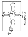
A solution for tuning the tunable impedance is shown in FIG. 2. Here, a hybrid transformer of the EBD is represented as a 4-port circuit element. In clockwise order starting from the left side, the ports of the EBD are connected to the antenna, the low-noise amplifier (LNA, not shown) of the RX-chain, ZBAL and the power amplifier (PA, not shown) of the TX-chain. A tuner is provided on the antenna side for reducing antenna impedance variations present under environmental disturbances near the antenna near-field. With reduced variations, it is more feasible to tune the balance network to track the remaining variation and optimize the balance condition while simultaneously optimizing the PA efficiency.
Hybrid couplers connected to VX+ and VX−, are subsequently connected to amplitude and phase difference detectors that can measure the waves moving back and forth between the hybrid transformer and the load port (e.g. RX, BAL, PA, and ANT). In this way, it is possible to measure all transfer functions from any port to any other port. Such transfer functions can be captured in so-called S-parameters. The following generic 4-port matrix would define the transfer characteristics according to the waves that such a hybrid coupler-based sensing system can observe:
[ b 1 b 2 b 3 b 4 ] = [ S 11 S 12 S 13 S 14 S 21 S 22 S 23 S 24 S 31 S 23 S 33 S 34 S 41 S 24 S 34 S 44 ] [ a 1 a 2 a 3 a 4 ] ,
where ai and bi, are the waves as defined by S-parameter theory for all ports, and port 1 is the ANT port, port 2 the PA/TX port, port 3 is the ZBAL port, and port 4 is the LNA/RX port.
A strategy is to observe all scattering parameters (S-parameters), and calculate from all those parameters the reflection required at the BAL port that will provide electrical balance, from which the BAL impedance needed for electrical balance can also be derived. For any given time instant, under the assumption that the antenna remains constant during a sufficiently long period in time for the algorithm to run, the waves are used to derive S-parameters, giving direct system-state information that can concurrently be used to calculate the optimized ZBAL that enables signal cancellation of a signal generated in the PA/TX.
This solution has the disadvantage that it is complex in design, and thus expensive to implement. Furthermore, the couplers have the disadvantage of being large components which are lossy when integrated on typical silicon technologies. This solution also does not allow for real-time balancing of the electrical balance duplexer, as it requires reducing antenna impedance variations before calculation of all the S-parameters requires tuning of both the antenna's port impedance and the tunable impedance.
Another solution for balancing an electrical balance duplexer is shown in WO 2013/063506 A2. This solution is also complex in design and requires the tuning of an antenna impedance and a tunable impedance.
SUMMARY
It is an aim of the present disclosure to provide embodiments for impedance balancing in a telecommunications device having an electrical balance duplexer.
This aim is achieved according to the present disclosure with a telecommunications device showing the technical characteristics of the characterizing part of the first claim.
Therefore, the present disclosure provides a telecommunications device comprising an electrical balance duplexer and a tuning circuit. The electrical balance duplexer is connected to an output node of a transmission path, to an input node of a receive path, to an antenna and to a tunable impedance. The electrical balance duplexer is configured to isolate the transmission path from the receive path by tuning the tunable impedance. The tuning circuit is provided for tuning the tunable impedance. The tuning circuit comprises amplitude detectors for measuring a voltage amplitude at each of the connections between the electrical balance duplexer on the one hand and the transmission path, the receive path and the tunable impedance on the other hand. The tuning circuit comprises phase detectors for measuring a voltage phase difference between any two of the connections between the electrical balance duplexer on the one hand and the transmission path, the receive path and the tunable impedance on the other hand. Hence, the tuning circuit comprises a phase detector for measuring a voltage phase difference between on the one hand the connection between the electrical balance duplexer and the transmission path and on the other hand the connection between the electrical balance duplexer and the tunable impedance, another phase detector for measuring a voltage phase difference between on the one hand the connection between the electrical balance duplexer and the transmission path and on the other hand the connection between the electrical balance duplexer and the receive path, and yet another measuring a voltage phase difference between on the one hand the connection between the electrical balance duplexer and the receive path and on the other hand the connection between the electrical balance duplexer and the tunable impedance. The tuning circuit comprises an impedance sensor for measuring the input impedance of the electrical balance duplexer at the connection between the electrical balance duplexer and the tunable impedance. The tuning circuit comprises a processing unit operatively connected to the detectors and to the tunable impedance. The processing unit is configured for calculating an optimized impedance value from the voltage amplitudes, the voltage phase differences and the impedance measured by the detectors. The processing unit is configured for tuning the tunable impedance towards the optimized impedance value.
In an example embodiment, the output of these detectors is sufficient to derive an approximation of the complete system of the electrical balance duplexer, and thus is sufficient to calculate an optimized impedance value for the tunable impedance, or at least a good first estimate for the optimized impedance value. This can allow the design of the tuning circuit to be greatly simplified, which can make the telecommunications device according to the present disclosure less expensive and more energy efficient and as such provide comparatively better RF performance.
The limited amount of data for the calculation of the optimized impedance value also permits the optimized impedance value of the tunable impedance to be calculated quickly, thereby enabling real-time tuning of the tunable impedance and thus balancing of the electrical balance duplexer. This also permits an inexpensive processing unit to be used for calculating the optimized impedance value, thereby further reducing the costs and energy consumption of the telecommunications device according to the present disclosure.
It is understood that the amplitude detectors, the phase detectors and the impedance detector may be implemented in different ways. They may for example be implemented as independent sensing circuits or elements which directly provide the amplitude, phase difference and impedance information to the processing unit. They may however, as another example, also be implemented by means of independent voltage detectors at each of the connections between the electrical balance duplexer on the one hand and the transmission path, the receive path and the tunable impedance on the other hand. Then, the processing unit may be provided for calculating the amplitude, phase difference and impedance information from the voltages detected by the voltage detectors.
In an embodiment of the telecommunications device according to the present disclosure the processing unit is configured for calculating the optimized impedance value from at least four scattering parameters between any two of the transmission path, the receive path and the tunable impedance. In some embodiments, the processing unit is configured for calculating the optimized impedance value from four scattering parameters, between any two of the transmission path, the receive path and the tunable impedance. The scattering parameters are calculated from the voltage amplitudes, the voltage phase differences and the impedance measured by the detectors.
In an example embodiment, a limited or reduced set of scattering parameters (S-parameters) can serve as an approximation of the complete S-parameter system of equations and thus be sufficient to calculate an optimized impedance value for the tunable impedance, or at least a good first estimate for the optimized impedance value. Furthermore, in some embodiments, this limited set of S-parameters may be approximated using amplitude and phase information from the detectors of the tuning circuit according to the present disclosure. This can allow the design of the tuning circuit to be greatly simplified, which can make the telecommunications device according to the present disclosure less expensive and more energy efficient and as such provide comparatively better RF performance.
Reducing the number of scattering parameters that are used for calculating an optimized impedance value increases the speed with which the optimized impedance value can be calculated, and thus improves upon the ability of the communications device to perform real-time tuning of the tunable impedance and thus balancing of the electrical balance duplexer.
In an embodiment of the telecommunications device according to the present disclosure the processing unit is configured for iteratively calculating the optimized impedance value and tuning the tunable impedance towards the optimized impedance value.
In an example embodiment, any difference between the first calculation of the optimized impedance value and a true optimized impedance value, caused by any approximations made in the equations for calculating the optimized impedance value, may be reduced quickly by iteratively repeating the tuning of the tunable impedance based on the amplitude and phase data obtained by the same detectors. In this way, the use of additional components for further improving the tuning of the tunable impedance to the optimized impedance value, can be avoided.
Because of the simplification in the calculation of the optimized impedance value, these iterative calculations are performed quickly, such that the further tuning of the tunable impedance and thereby balancing of the electrical balance duplexer may still be performed in real-time.
In some embodiments, the tuning of the tunable impedance is repeated until the scattering parameter from the transmission path to the receive path, which is an indicator for isolation of the transmission path from the receive path and may be calculated from the amplitude and phase data from the amplitude and phase detectors at the transmission path and the receive path, is below a predetermined threshold value.
In an embodiment of the telecommunications device according to the present disclosure, at least one of the detectors is implemented by means of a root mean square (rms) voltage detector.
Implementing the detectors of the telecommunications device according to an embodiment of the present disclosure by means of rms voltage detectors, instead of more bulky and/or lossy components, can permit a further simplifying of the design of the communications device.
In an embodiment of the telecommunications device according to the present disclosure, the impedance detector is implemented by means of the amplitude detector at the connection between the electrical balance duplexer and the tunable impedance, for example in combination with voltage phase detecting means for detecting the voltage phase at the connection, a power source for providing a reference current, and optionally additional phase detecting means for detecting the phase of the reference current.
In an example embodiment, the impedance detector of the tuning circuit may be implemented by means of a power source providing a reference current and the amplitude detector at the connection between the electrical balance duplexer and the tunable impedance in combination with phase detecting means for detecting the voltage phase at the connection, and optionally also phase detecting means for detecting a phase of the reference current. If the tunable impedance is then temporarily disconnected, then the input impedance of the electrical balance duplexer at the connection between the electrical balance duplexer and the tunable impedance is easily calculated from the reference current and the measured amplitude and phase data. The use of the same detector can allow further simplifying the design of the circuit.
The present disclosure further provides a method for tuning a tunable impedance of a telecommunications device comprising an electrical balance duplexer. The electrical balance duplexer of the telecommunications device is connected to an output node of a transmission path, to an input node of a receive path, to an antenna and to the tunable impedance. The electrical balance duplexer is configured to isolate the transmission path from the receive path by tuning the tunable impedance. The method comprises the step of measuring a voltage amplitude at each of the connections between the electrical balance duplexer on the one hand and the transmission path, the receive path and the tunable impedance on the other hand. The method comprises the step of measuring a voltage phase difference between any two of the connections between the electrical balance duplexer on the one hand and the transmission path, the receive path and the tunable impedance on the other hand. The method comprises the step of measuring an input impedance of the electrical balance duplexer at the connection between the electrical balance duplexer and the tunable impedance. The method comprises the step of calculating an optimized impedance value from the measured voltage amplitudes, voltage phase differences and impedance. The method comprises the step of tuning the tunable impedance towards the optimized impedance value.
For the discussion of the method according to the present disclosure there is referred to the discussion of the telecommunications device according to the present disclosure.
In an embodiment of the method according to the present disclosure the optimized impedance value is calculated from at least four scattering parameters between any two of the transmission path, the receive path and the tunable impedance. The scattering parameters are calculated from the measured voltage amplitudes, voltage phase differences and impedance.
In an embodiment of the method according to the present disclosure the steps of the method are iteratively repeated until a scattering parameter from the transmission path to the receive path is below a predetermined threshold value.
The scattering parameter is calculated from the measured voltage amplitudes at the connection between the electrical duplexer on the one hand and the transmission path and the receive path on the other hand, and from the measured voltage phase difference between the connections between the electrical duplexer on the one hand and the transmission path and the receive path on the other hand.
In an embodiment of the method according to the present disclosure the method is provided for tuning the tunable impedance of the telecommunications device according to an embodiment of the present disclosure.
BRIEF DESCRIPTION OF THE FIGURES
The disclosure will be further elucidated by means of the following description and the appended figures.
FIG. 1 shows an electrical balance duplexer.
FIG. 2 shows a prior art tuning circuit for tuning the tunable impedance of an electrical balance duplexer of the state of the art.
FIG. 3 shows an electrical balance duplexer assumed as a 3-port network.
FIG. 4 shows a schematic representation of the electronics communication device, according to example embodiments.
FIG. 5 shows a schematic representation of the tuning circuit of the electronic communication device, according to example embodiments.
FIG. 6 shows an impedance detector of the electronics communication device, according to example embodiments.
FIG. 7 shows an example implementation of an amplitude detector of the electronics communication device, according to example embodiments.
FIG. 8 shows an example implementation of a phase detector of the electronics communication device, according to example embodiments.
DETAILED DESCRIPTION
The present disclosure will be described with respect to particular embodiments and with reference to certain drawings but the disclosure is not limited thereto but only by the claims. The drawings described are only schematic and are non-limiting. In the drawings, the size of some of the elements may be exaggerated and not drawn on scale for illustrative purposes. The dimensions and the relative dimensions do not necessarily correspond to actual reductions to practice of the disclosure.
Furthermore, the terms first, second, third and the like in the description and in the claims, are used for distinguishing between similar elements and not necessarily for describing a sequential or chronological order. The terms are interchangeable under appropriate circumstances and the embodiments of the disclosure can operate in other sequences than described or illustrated herein.
Moreover, the terms top, bottom, over, under and the like in the description and the claims are used for descriptive purposes and not necessarily for describing relative positions. The terms so used are interchangeable under appropriate circumstances and the embodiments of the disclosure described herein can operate in other orientations than described or illustrated herein.
The term “comprising”, used in the claims, should not be interpreted as being restricted to the means listed thereafter; it does not exclude other elements or steps. It should be interpreted as specifying the presence of the stated features, integers, steps or components as referred to, but does not preclude the presence or addition of one or more other features, integers, steps or components, or groups thereof. Thus, the scope of the expression “a device comprising means A and B” should not be limited to devices consisting only of components A and B. It means that with respect to the present disclosure, the only relevant components of the device are A and B.
FIG. 3 shows the electrical balance duplexer 1 when assuming that it is a 3-port network with the antenna 4 included in the S-parameter representation of the electrical balance duplexer 1. The reason for the inclusion of the antenna 4 is that we assume the antenna 4 to be an unknown impedance that also varies over time. In that case, the S-parameters describing all the transfer paths throughout the 3-port network are given as:
[ b 1 b 2 b 3 ] = [ S 11 S 12 S 13 S 21 S 22 S 23 S 31 S 32 S 33 ] [ a 1 a 2 a 3 ] ,
where the first port (PA/TX port) is the connection to the transmission path 2, the second port is the connection to the tunable impedance 5 (balance network Zbal), and the third port (LNA/RX port) is the connection to the receive path 3.
The disclosure provides a tuning circuit 6 with a sensing method that derives the equations in order to calculate Zbal in real-time and provide automated tuning, using minimal hardware, for any antenna condition.
As also already mentioned, considering the problem in a 3-port fashion helps to simplify the problem, and allows the use of less hardware. FIG. 4 shows the same 3-port network with a tuning circuit 6, of which more detail is shown in FIG. 5, connected to the three ports (in a schematic sense), and provides a closed-loop that tunes Zbal to achieve isolation. The embodiment assumes a test signal is available from the transmitter TX, and that an optimized Zbal exists for any signal frequency at which the transmitter TX is active.
In the case where all 9 S-parameters (the full matrix) would be known, it would be possible to calculate the associated Zbal for achieving isolation in the duplexer 1 in a single step. However, we solve the problem of finding Zbal in an iterative manner, with practically implementable (cheap, low-power, low-area, etc.) sensors on as little nodes as possible.
In particular, the algorithm uses the sensed information using detectors or sensors 7, 8, 9 at just the TX, RX and BAL ports, thus respectively the connections between the electrical balance duplexer 1 on the one hand and the transmission path 2, the receive path 3 and the tunable impedance 5 on the other hand, to solve the following equations derived from the S-parameter matrix to arrive at Zbal, using only S13, S12, S23 and S22 (4 out of 9 parameters):
S 13 + Γ 2 S 12 S 23 1 + S 22 Γ 2 = 0 Γ 2 = - S 13 S 12 S 23 + S 13 S 22 Γ 2 = Z bal - Z 0 Z bal + Z 0 Z bal = Z 0 1 + Γ 2 1 - Γ 2
where Sij is the S-parameter that describes the transfer from port i to j, and Γi describes the so-called reflection coefficient, which is calculated from a limited amount of S-parameters (not all 9 are used). This directly limits the associated hardware to solve the equation.
Note that, although a first approximation of Zbal may already be calculated from the 4 S-parameters in a first calculation based on a single measurement from the detectors 7, 8, 9, the calculated Zbal may still not be optimized due to a number of assumptions on, for example, what the input and load impedances are on all ports. The provided equations are thus not always able to give a fully accurate answer for Zbal in a single calculation based on the detected information. Therefore, the algorithm is further optimized by iterating a number of times to improve upon possible differences or deviations caused by the assumptions in the equations.
In an example practical embodiment, amplitude sensors 7 can be used to observe amplitude or magnitude information at all nodes, and phase detectors 8 could be used to observe the phase information. Then, from that information, the set of 4 S-parameters can be derived, with simpler hardware.
In that case, the following equations may be solved first, before finally solving the equation for Zbal (as shown above).
S 12 = ( Z 1 ) ( Z 2 ) 1 2 ( 1 + Z 2 * Z bal ) V 2 V 1 e ( φ 2 - φ 1 ) j S 13 = ( Z 1 ) ( Z 3 ) V 3 V 1 e ( φ 3 - φ 1 ) j S 32 = ( Z 3 ) ( Z 2 ) 1 2 ( 1 - Z 2 Z bal ) V 2 V 3 e ( φ 2 - φ 3 ) j S 22 = Z 2 - Z bal * Z 2 + Z bal
Where j is the imaginary number operator, Zi is the impedance looking into the electrical balance duplexer, in this case a hybrid transformer, at port i, |Vi| is the voltage amplitude detected at port i,
Figure US09948446-20180417-P00001
(Zi) is the real part of impedance Zi and φi is the phase of the voltage at port i. Note that S22 relates to Z2 and Z2*, which is the input impedance of the electrical balance duplexer 1 at the connection between the electrical balance duplexer 1 and the tunable impedance 5, and thus the impedance seen when looking into the hybrid transformer 5 from the balance network port.
To arrive at these equations, it is assumed that the antenna impedance negligibly influences Z2. It is also assumed that the tunable impedance Zbal is known or can be measured. It is also assumed that the impedance of the transmission path 2 is matched to the impedance of the electrical balance duplexer 1 at the connection between both, and that the impedance of the receive path 3 is matched to the impedance of the electrical balance duplexer 1 at the connection between both. Thus, the PA and LNA are matched to their respective ports. For example, if PA output impedance=25Ω, then Z1=25Ω. And if LNA input impedance=100Ω, then Z3=100Ω. It is also assumed that the network is reciprocal network. i.e. Sij=Sji. It is also assumed that the S-parameters between ports (e.g. Sij between port i and j) are simplified to be the transfer function of the output over the input signal. For example, S31=b3/a1.
From these equations, it becomes clear that a necessary condition is that the impedance Z2 should be known. With Z2 being the input impedance looking into the electrical balance duplexer 1 at the BAL-port interface, i.e. the connection between the electrical balance duplexer 1 and the tunable impedance 5.
FIG. 5 shows block level diagram of a tuning circuit of an electronic communication device according to an embodiment of the present disclosure. In this embodiment, analog voltages and phases at the ports of the EBD are measured by means of amplitude detectors 7, phase detectors 8 and an impedance detector 9 partially implemented by means of an amplitude detector 9 as shown in FIG. 6. The measured data is digitized by means of analog-to-digital converters ADC, and forwarded to the processing unit 10 where it is used for tuning the tunable impedance 5 according to an embodiment of the method of the present disclosure.
FIG. 6 shows an example impedance detector or sensor 9 that could be used to sense both Z2 as well as provide a calibration engine for Zbal (a-priori to live operation), using a three-way switch and two voltage sensors (connected to terminals V2 and V2′). Vref is an RF voltage that could be derived from the transmitter, and operation for this test could be performed at low-power, i.e. tapped from prior to the PA.
For each port, an amplitude (RMS) detector 7 (magnitude sensor) would be required. An implementation of one such magnitude sensor which could be used in the example diode-connected FET device shown in FIG. 7. Between two ports, a phase detector 8, such as for example shown in FIG. 8, could be used to measure the voltage phase difference φi−φj. It should however be clear that shown amplitude detectors 7 and phase detectors 8 are only example implementations, and different types of suitable detectors may be used.
Various mathematical assumptions and simplifications can be applied for the implementation of an algorithm that can arrive at a value for Zbal for any antenna impedance Zant within 1.5:1 VSWR even when the detectors/ sensors 7, 8, 9 exhibit up to 20% voltage error, 10 degrees phase error, and 20% error in Z2. This is true even for a hybrid transformer 1 that is not symmetric, i.e. ZBAL≠ZANT. For example, typical hybrid transformer implementations use skewing to favor TX over RX loss, and have capacitive coupling which means that single-ended EBDs (FIG. 1) can have asymmetric values (by nature).
The algorithm, in pseudocode, operates as follows:
1: put Zbal(0) = 50 Ω
2: evaluate Γ2(0)
3: evaluate Z c ( 0 ) = Z 0 1 - Γ 2 ( 0 ) 1 - Γ 2 ( 0 )
4: put Zbal(1) = Zc(0)
5: i = 1
6: while S13 < Threshold do
Figure US09948446-20180417-P00002
 Ex.: Threshold = −50 dB
7:  evaluate Γ2(i)
8:  evaluate Zc(i)
9:  Corr = 50 Ω − Zc(i)
10:  put Zbal(i + 1) = Zbal(i) − K * Corr
Figure US09948446-20180417-P00003
 K = attenuation factor
11: i++

In optimization, Z0, the Threshold factor and attenuation factor K are found such that the algorithm finds Zbal in as low as possible iterations.
The method according to a further embodiment of the present disclosure thus comprises the steps of: setting the tunable impedance 5 to a predetermined initial value, e.g. 50Ω, calculating a reflection coefficient Γ2 at the side of the electrical balance duplexer 1 connected to the tunable impedance 5 from values measured by the detectors 7, 8, 9 of the tuning circuit 6, calculating a first estimate of the optimized impedance value from the predetermined initial value of the tunable impedance 5 and the calculated reflection coefficient Γ2, and setting the tunable impedance 5 to the first estimate of the optimized impedance value.
In some embodiments, the method further comprises the steps of: recalculating the reflection coefficient Γ2, calculating an intermediate value of the optimized impedance value from the previous estimate of the optimized impedance value and the recalculated reflection coefficient Γ2, calculating a correction term Corr by subtracting the calculated intermediate value from the predetermined initial value, calculating a further estimate of the optimized impedance value by subtracting the correction term Corr from the predetermined initial value, optionally after multiplying the correction term with an attenuation factor K, and setting the tunable impedance to the further estimate of the optimized impedance value. In some embodiments, these steps are iteratively repeated until the value of the scattering parameter S13 from transmission path 2 to the receive path 3, which scattering parameter S13 is calculated from measurements of the detectors 7, 8, 9 at the connections between the electrical balance duplexer 1 on the one hand and the transmission path 2 and the receive path 3 on the other hand, is smaller than a predetermined threshold value, below which threshold value the transmission path 2 is substantially isolated from the receive path 3.

Claims (20)

What is claimed is:
1. A telecommunications device comprising:
an electrical balance duplexer connected to an output node of a transmission path, an input node of a receive path, an antenna, and a tunable impedance, wherein the electrical balance duplexer is configured to isolate the transmission path from the receive path by tuning the tunable impedance; and
a tuning circuit for tuning the tunable impedance,
wherein the tuning circuit comprises:
amplitude detectors for measuring voltage amplitudes at each of the connections between the electrical balance duplexer and the transmission path, between the electrical balance duplexer and the receive path, and between the electrical balance duplexer and the tunable impedance;
phase detectors for measuring voltage phase differences between each of the connections between the electrical balance duplexer and the transmission path, between the electrical balance duplexer and the receive path, and between the electrical balance duplexer and the tunable impedance;
an impedance sensor for measuring an input impedance of the electrical balance duplexer at the connection between the electrical balance duplexer and the tunable impedance; and
a processing unit operatively connected to the amplitude detectors, the phase detectors, the impedance sensor, and the tunable impedance, wherein the processing unit is configured to:
calculate an optimized impedance value from the voltage amplitudes, the voltage phase differences, and the input impedance of the electrical balance duplexer; and
tune the tunable impedance towards the optimized impedance value.
2. The telecommunications device according to claim 1, wherein the processing unit is further configured to calculate the optimized impedance value from at least four scattering parameters between any two of the transmission path, the receive path, and the tunable impedance, wherein the scattering parameters are calculated from the voltage amplitudes, the voltage phase differences, and the input impedance.
3. The telecommunications device according to claim 1, wherein the processing unit is further configured to iteratively calculate the optimized impedance value and tune the tunable impedance towards the optimized impedance value.
4. The telecommunications device according to claim 1, wherein at least one of the detectors is implemented using a root mean square (rms) voltage detector.
5. The telecommunications device according to claim 1, wherein the impedance sensor is implemented using the amplitude detector at the connection between the electrical balance duplexer and the tunable impedance.
6. The telecommunications device according to claim 1, wherein the tuning circuit further comprises an analog-to-digital converter configured to digitize the voltage amplitudes, the voltage phase differences, and the input impedance.
7. A method for tuning a tunable impedance of a telecommunications device comprising an electrical balance duplexer connected to an output node of a transmission path, an input node of a receive path, an antenna, and the tunable impedance, wherein the electrical balance duplexer is configured to isolate the transmission path from the receive path by tuning the tunable impedance, the method comprising:
measuring voltage amplitudes at each of the connections between the electrical balance duplexer and the transmission path, between the electrical balance duplexer and the receive path, and between the electrical balance duplexer and the tunable impedance;
measuring voltage phase differences between each of the connections between the electrical balance duplexer and the transmission path, between the electrical balance duplexer and the receive path, and between the electrical balance duplexer and the tunable impedance;
measuring an input impedance of the electrical balance duplexer at the connection between the electrical balance duplexer and the tunable impedance;
calculating an optimized impedance value from the measured voltage amplitudes, the voltage phase differences, and the input impedance; and
tuning the tunable impedance towards the optimized impedance value.
8. The method according to claim 7, wherein the optimized impedance value is calculated from at least four scattering parameters between any two of the transmission path, the receive path, and the tunable impedance, and wherein the scattering parameters are calculated from the measured voltage amplitudes, the measured voltage phase differences, and the input impedance.
9. The method according to claim 7, wherein the steps of the method are iteratively repeated until a scattering parameter from the transmission path to the receive path is below a predetermined threshold value.
10. The method according to claim 7, wherein calculating an optimized impedance value from the measured voltage amplitudes, the voltage phase differences, and the input impedance, and tuning the tunable impedance towards the optimized impedance value are performed iteratively.
11. The method according to claim 7, wherein measuring the voltage amplitudes or measuring the voltage phase differences is performed using a root mean square (rms) voltage detector.
12. The method according to claim 7, wherein measuring the input impedance is performed using an amplitude detector at the connection between the electrical balance duplexer and the tunable impedance.
13. The method according to claim 7, further comprising digitizing the voltage amplitudes, the voltage phase differences, and the input impedance.
14. A tuned impedance for a telecommunications device comprising an electrical balance duplexer connected to an output node of a transmission path, an input node of a receive path, an antenna, and the tuned impedance, wherein the electrical balance duplexer is configured to isolate the transmission path from the receive path by tuning the tuned impedance, and wherein the tuned impedance is tuned according to a method comprising:
measuring voltage amplitudes at each of the connections between the electrical balance duplexer and the transmission path, between the electrical balance duplexer and the receive path, and between the electrical balance duplexer and the tuned impedance;
measuring voltage phase differences between each of the connections between the electrical balance duplexer and the transmission path, between the electrical balance duplexer and the receive path, and between the electrical balance duplexer and the tuned impedance;
measuring an input impedance of the electrical balance duplexer at the connection between the electrical balance duplexer and the tuned impedance;
calculating an optimized impedance value from the measured voltage amplitudes, the voltage phase differences, and the input impedance; and
tuning the tuned impedance towards the optimized impedance value.
15. The tuned impedance according to claim 14, wherein the optimized impedance value is calculated from at least four scattering parameters between any two of the transmission path, the receive path, and the tuned impedance, and wherein the scattering parameters are calculated from the measured voltage amplitudes, the measured voltage phase differences, and the input impedance.
16. The tuned impedance according to claim 14, wherein the steps of the method are iteratively repeated until a scattering parameter from the transmission path to the receive path is below a predetermined threshold value.
17. The tuned impedance according to claim 14, wherein calculating an optimized impedance value from the measured voltage amplitudes, the voltage phase differences, and the input impedance, and tuning the tuned impedance towards the optimized impedance value are performed iteratively.
18. The tuned impedance according to claim 14, wherein measuring the voltage amplitudes or measuring the voltage phase differences is performed using a root mean square (rms) voltage detector.
19. The tuned impedance according to claim 14, wherein measuring the input impedance is performed using an amplitude detector at the connection between the electrical balance duplexer and the tuned impedance.
20. The tuned impedance according to claim 14, wherein the method further comprises digitizing the voltage amplitudes, the voltage phase differences, and the input impedance.
US15/292,370 2015-12-24 2016-10-13 Telecommunications device comprising an electrical balance duplexer and method for balancing the electrical balance duplexer Expired - Fee Related US9948446B2 (en)

Applications Claiming Priority (3)

Application Number Priority Date Filing Date Title
EP15202762 2015-12-24
EP15202762.9 2015-12-24
EP15202762.9A EP3185426B1 (en) 2015-12-24 2015-12-24 Telecommunications device comprising an electrical balance duplexer and a method for balancing said electrical balance duplexer

Publications (2)

Publication Number Publication Date
US20170187510A1 US20170187510A1 (en) 2017-06-29
US9948446B2 true US9948446B2 (en) 2018-04-17

Family

ID=55024950

Family Applications (1)

Application Number Title Priority Date Filing Date
US15/292,370 Expired - Fee Related US9948446B2 (en) 2015-12-24 2016-10-13 Telecommunications device comprising an electrical balance duplexer and method for balancing the electrical balance duplexer

Country Status (2)

Country Link
US (1) US9948446B2 (en)
EP (1) EP3185426B1 (en)

Cited By (2)

* Cited by examiner, † Cited by third party
Publication number Priority date Publication date Assignee Title
US10938542B1 (en) * 2019-09-25 2021-03-02 Apple Inc. Electrical balanced duplexer-based duplexer
US20210359754A1 (en) * 2020-05-14 2021-11-18 Jeeva Wireless Inc. Duplex long range backscatter wireless communication systems and methods

Families Citing this family (5)

* Cited by examiner, † Cited by third party
Publication number Priority date Publication date Assignee Title
EP3185426B1 (en) * 2015-12-24 2019-02-06 IMEC vzw Telecommunications device comprising an electrical balance duplexer and a method for balancing said electrical balance duplexer
EP3522380B1 (en) 2018-01-31 2020-12-02 u-blox AG Apparatus for duplexing signals, wireless communications device and method of duplexing signals
US10742253B2 (en) * 2018-06-22 2020-08-11 Qorvo Us, Inc. Radio frequency front-end apparatus
US10812049B2 (en) * 2018-09-06 2020-10-20 Apple Inc. Reconfigurable feed-forward for electrical balance duplexers (EBD)
US10530615B1 (en) * 2019-03-08 2020-01-07 Apple Inc. Adaptive power equalization in electrical balance duplexers

Citations (8)

* Cited by examiner, † Cited by third party
Publication number Priority date Publication date Assignee Title
US5159703A (en) * 1989-12-28 1992-10-27 Lowery Oliver M Silent subliminal presentation system
WO2013063506A2 (en) 2011-10-26 2013-05-02 Qualcomm Incorporated Impedance balancing for transmitter to receiver rejection
EP2672631A1 (en) 2012-06-07 2013-12-11 Telefonaktiebolaget L M Ericsson (publ) Duplexer-less transceiver and communication apparatus
US20130343237A1 (en) * 2010-06-03 2013-12-26 Broadcom Corporation Front End Module With Tone Injection
US20140176388A1 (en) * 2012-12-21 2014-06-26 Imec Tunable impedance network
WO2014173459A1 (en) 2013-04-26 2014-10-30 Telefonaktiebolaget L M Ericsson (Publ) Transceiver arrangement, communication device, method and computer program
US20160294436A1 (en) * 2014-10-29 2016-10-06 Telefonaktiebolaget L M Ericsson (Publ) Transceiver Arrangement and Communication Device
US20170187510A1 (en) * 2015-12-24 2017-06-29 Imec Vzw Telecommunications Device Comprising an Electrical Balance Duplexer and Method for Balancing the Electrical Balance Duplexer

Patent Citations (10)

* Cited by examiner, † Cited by third party
Publication number Priority date Publication date Assignee Title
US5159703A (en) * 1989-12-28 1992-10-27 Lowery Oliver M Silent subliminal presentation system
US20130343237A1 (en) * 2010-06-03 2013-12-26 Broadcom Corporation Front End Module With Tone Injection
WO2013063506A2 (en) 2011-10-26 2013-05-02 Qualcomm Incorporated Impedance balancing for transmitter to receiver rejection
US9083441B2 (en) * 2011-10-26 2015-07-14 Qualcomm Incorporated Impedance balancing for transmitter to receiver rejection
EP2672631A1 (en) 2012-06-07 2013-12-11 Telefonaktiebolaget L M Ericsson (publ) Duplexer-less transceiver and communication apparatus
US9667404B2 (en) * 2012-06-07 2017-05-30 Telefonaktiebolaget Lm Ericsson (Publ) Duplexer-less transceiver and communication apparatus
US20140176388A1 (en) * 2012-12-21 2014-06-26 Imec Tunable impedance network
WO2014173459A1 (en) 2013-04-26 2014-10-30 Telefonaktiebolaget L M Ericsson (Publ) Transceiver arrangement, communication device, method and computer program
US20160294436A1 (en) * 2014-10-29 2016-10-06 Telefonaktiebolaget L M Ericsson (Publ) Transceiver Arrangement and Communication Device
US20170187510A1 (en) * 2015-12-24 2017-06-29 Imec Vzw Telecommunications Device Comprising an Electrical Balance Duplexer and Method for Balancing the Electrical Balance Duplexer

Non-Patent Citations (3)

* Cited by examiner, † Cited by third party
Title
European Search Report, European Patent Application No. 15202762, dated Jun. 9, 2016, 4 pages.
Laughlin, Leo et al., "Passive and Active Electrical Balance Duplexers", IEEE Transactions on Circuits and Systems-II: Express Briefs, vol. 63, No. 1, Jan. 2016, pp. 94-98.
Laughlin, Leo et al., "Passive and Active Electrical Balance Duplexers", IEEE Transactions on Circuits and Systems—II: Express Briefs, vol. 63, No. 1, Jan. 2016, pp. 94-98.

Cited By (5)

* Cited by examiner, † Cited by third party
Publication number Priority date Publication date Assignee Title
US10938542B1 (en) * 2019-09-25 2021-03-02 Apple Inc. Electrical balanced duplexer-based duplexer
US11438131B2 (en) 2019-09-25 2022-09-06 Apple Inc. Electrical balanced duplexer-based duplexer
US11791974B2 (en) 2019-09-25 2023-10-17 Apple Inc. Electrical balanced duplexer-based duplexer
US20210359754A1 (en) * 2020-05-14 2021-11-18 Jeeva Wireless Inc. Duplex long range backscatter wireless communication systems and methods
US11843450B2 (en) * 2020-05-14 2023-12-12 Jeeva Wireless Inc. Duplex long range backscatter wireless communication systems and methods

Also Published As

Publication number Publication date
US20170187510A1 (en) 2017-06-29
EP3185426A1 (en) 2017-06-28
EP3185426B1 (en) 2019-02-06

Similar Documents

Publication Publication Date Title
US9948446B2 (en) Telecommunications device comprising an electrical balance duplexer and method for balancing the electrical balance duplexer
EP1915819B1 (en) Integrated load impedance sensing for tunable matching networks
US9722713B2 (en) Architecture and control of analog self-interference cancellation
KR101944592B1 (en) Voltage standing wave ratio measurement and tuning systems and methods
CN104718713B (en) Method and apparatus for antenna calibration
US8565695B2 (en) Detection of the value of an impedance of a radiofrequency system
US9947985B2 (en) System and method for a directional coupler
Laughlin et al. Passive and active electrical balance duplexers
KR101967046B1 (en) Communication device and method for determining a load impedance
Jain et al. A 10GHz CMOS RX frontend with spatial cancellation of co-channel interferers for MIMO/digital beamforming arrays
US20130038502A1 (en) Controller for a radio circuit
KR102468231B1 (en) Apparatus and method for matching antenna impedence in wireless communication system
US10107843B2 (en) Low power on-chip impedance detector
AU2017230236B2 (en) Apparatus and method for impedance measurement and adaptive antenna tuning
CN101019032A (en) Circuit for detecting the impedance of a load
US20160036482A1 (en) Apparatus and method for antenna tuning
US10666219B2 (en) Automatic impedance matching method and module, particularly for a radio-frequency transmission or reception chain
US20200007092A1 (en) Amplification in Presence of a Variable Antenna Impedance
CN104821869B (en) Duplex apparatus, wireless device and related methods
US20130324057A1 (en) Determining a delivered power estimate and a load impedance estimate using a directional coupler
KR102409687B1 (en) Method and apparatus for measuring chareteristic of radio frequency chain
US20110115507A1 (en) Power delivery circuit monitoring
US20130207710A1 (en) Enhanced Flexibility Coupler for RF Power Detection and Control
KR102417241B1 (en) Self-Interference Cancelator of Millimeter wave transceiver
EP2477338A1 (en) Interface circuit

Legal Events

Date Code Title Description
AS Assignment

Owner name: IMEC VZW, BELGIUM

Free format text: ASSIGNMENT OF ASSIGNORS INTEREST;ASSIGNORS:VAN LIEMPD, BAREND WILHELMUS MARINUS;HERSHBERG, BENJAMIN;FIEVET, NATHALIE;SIGNING DATES FROM 20161018 TO 20161111;REEL/FRAME:041049/0105

Owner name: VRIJE UNIVERSITEIT BRUSSEL, BELGIUM

Free format text: ASSIGNMENT OF ASSIGNORS INTEREST;ASSIGNORS:VAN LIEMPD, BAREND WILHELMUS MARINUS;HERSHBERG, BENJAMIN;FIEVET, NATHALIE;SIGNING DATES FROM 20161018 TO 20161111;REEL/FRAME:041049/0105

STCF Information on status: patent grant

Free format text: PATENTED CASE

FEPP Fee payment procedure

Free format text: MAINTENANCE FEE REMINDER MAILED (ORIGINAL EVENT CODE: REM.); ENTITY STATUS OF PATENT OWNER: LARGE ENTITY

LAPS Lapse for failure to pay maintenance fees

Free format text: PATENT EXPIRED FOR FAILURE TO PAY MAINTENANCE FEES (ORIGINAL EVENT CODE: EXP.); ENTITY STATUS OF PATENT OWNER: LARGE ENTITY

STCH Information on status: patent discontinuation

Free format text: PATENT EXPIRED DUE TO NONPAYMENT OF MAINTENANCE FEES UNDER 37 CFR 1.362

FP Lapsed due to failure to pay maintenance fee

Effective date: 20220417