US9913355B2 - Method of forming a sequencing system and structure therefor - Google Patents
Method of forming a sequencing system and structure therefor Download PDFInfo
- Publication number
- US9913355B2 US9913355B2 US14/804,166 US201514804166A US9913355B2 US 9913355 B2 US9913355 B2 US 9913355B2 US 201514804166 A US201514804166 A US 201514804166A US 9913355 B2 US9913355 B2 US 9913355B2
- Authority
- US
- United States
- Prior art keywords
- open circuit
- diagnostic
- circuit
- control unit
- integrated
- Prior art date
- Legal status (The legal status is an assumption and is not a legal conclusion. Google has not performed a legal analysis and makes no representation as to the accuracy of the status listed.)
- Active, expires
Links
Images


Classifications
-
- H05B37/036—
-
- H—ELECTRICITY
- H05—ELECTRIC TECHNIQUES NOT OTHERWISE PROVIDED FOR
- H05B—ELECTRIC HEATING; ELECTRIC LIGHT SOURCES NOT OTHERWISE PROVIDED FOR; CIRCUIT ARRANGEMENTS FOR ELECTRIC LIGHT SOURCES, IN GENERAL
- H05B47/00—Circuit arrangements for operating light sources in general, i.e. where the type of light source is not relevant
- H05B47/20—Responsive to malfunctions or to light source life; for protection
- H05B47/23—Responsive to malfunctions or to light source life; for protection of two or more light sources connected in series
-
- H05B33/0887—
-
- H—ELECTRICITY
- H05—ELECTRIC TECHNIQUES NOT OTHERWISE PROVIDED FOR
- H05B—ELECTRIC HEATING; ELECTRIC LIGHT SOURCES NOT OTHERWISE PROVIDED FOR; CIRCUIT ARRANGEMENTS FOR ELECTRIC LIGHT SOURCES, IN GENERAL
- H05B45/00—Circuit arrangements for operating light-emitting diodes [LED]
- H05B45/50—Circuit arrangements for operating light-emitting diodes [LED] responsive to malfunctions or undesirable behaviour of LEDs; responsive to LED life; Protective circuits
-
- G01R31/026—
-
- G—PHYSICS
- G01—MEASURING; TESTING
- G01R—MEASURING ELECTRIC VARIABLES; MEASURING MAGNETIC VARIABLES
- G01R31/00—Arrangements for testing electric properties; Arrangements for locating electric faults; Arrangements for electrical testing characterised by what is being tested not provided for elsewhere
- G01R31/50—Testing of electric apparatus, lines, cables or components for short-circuits, continuity, leakage current or incorrect line connections
- G01R31/54—Testing for continuity
Definitions
- Embodiments disclosed in the present invention relate generally to electrical technology, and more specifically to a circuit detection device which integrates fault reporting of a plurality of devices connected in a daisy chain arrangement.
- LEDs light emitting diodes
- ICs integrated circuits
- This arrangement does not provide detection of connectivity issues and a mechanism to relay a connection issue to a control unit. Since each LED load is part of a total system of lighting, any LED open load causes system degradation. In order to avoid system degradation due to an open load condition, all LEDs in the system must be turned off. Accordingly, it would be desirable to have LED sequencing drivers that incorporate an open circuit detection and reporting system.
- FIG. 1 illustrates a block diagram of a sequencing system in accordance with an embodiment of the present invention
- FIG. 2 schematically illustrates an embodiment of a portion of the sequencing system of FIG. 1 in accordance with an embodiment of the present invention
- FIG. 3 schematically illustrates an embodiment of a sequencing system in accordance with an embodiment of the present invention.
- asserted can be either a high voltage or high logic or a low voltage or low logic depending on whether positive or negative logic is used and negated may be either a low voltage or low state or a high voltage or high logic depending on whether positive or negative logic is used.
- negated may be either a low voltage or low state or a high voltage or high logic depending on whether positive or negative logic is used.
- negated may be either a low voltage or low state or a high voltage or high logic depending on whether positive or negative logic is used.
- FIG. 1 illustrates a block diagram of a sequencing system 10 .
- the sequencing system 10 may have a plurality of integrated circuits (IC) 11 a , 11 b , and 11 c .
- Each IC may have an input 17 , a sequence output 15 , and a diagnostic output 16 .
- the ICs may be connected in a daisy chain, wherein the sequence output of a first IC is electrically connected to the input of a second IC.
- the sequence output of the first IC 11 a may be electrically connected to the input of the second IC 11 b
- the sequence output of the second IC 11 b may be electrically connected to the input of a third IC 11 c , and so on.
- Each IC may also have a load output 14 , which may be electrically connected to a load 13 which may be controlled by input 17 .
- the load 13 may comprise an LED load.
- the LED load may contain one or more LEDs.
- the sequencing system 10 may also have a control unit 12 .
- the control unit 12 may be coupled to a first integrated circuit of the plurality of ICs, for example, element 11 a .
- the diagnostic output 16 of each individual IC 11 a , 11 b , 11 c may be electrically connected to the control unit 12 .
- the diagnostic output 16 may report an open circuit condition to the control unit 12 .
- the system illustrated in FIG. 1 illustrates a sequencing system 10 having three (3) ICs, however it is understood that the system may contain any number of ICs.
- FIG. 2 illustrates a portion of the sequencing system 10 of FIG. 1 .
- Each IC may have an input 17 , a sequence output 15 , and a diagnostic output 16 .
- the ICs may be connected in a daisy chain, wherein the sequence output of a first IC is electrically connected to the input of a second IC.
- the sequence output of the first IC 11 a may be electrically connected to the input of the second IC 11 b and the sequence output of the second IC 11 b may be electrically connected to the input of a third IC 11 c (shown in FIG. 1 ), and so on.
- Each IC may also have a load output 14 , which may be electrically connected to a load 13 .
- the load 13 may comprise an LED load.
- the LED load may contain one or more LEDs.
- functional circuitry for driving load output 14 is not shown.
- the sequencing system 10 may also have a control unit 12 .
- the control unit 12 may be a microprocessor and may also serve as a voltage source.
- the control unit 12 may be coupled to a first integrated circuit 11 a of the plurality of ICs.
- the control unit 12 may provide on/off control.
- the diagnostic output 16 may be electrically connected to the control unit 12 .
- the diagnostic output 16 may report an open circuit condition to the control unit 12 .
- FIG. 1 illustrates each IC 11 a , 11 b , 11 c having a diagnostic output 16 that may be electrically connected to the control unit 12 .
- the system illustrated in FIG. 2 illustrates a sequencing system 10 having two (2) ICs, however it is understood that the system may contain any number of ICs.
- Each IC 11 a , 11 b may have a diagnostic circuit.
- the diagnostic circuit may detect an open circuit condition if the intermediate communication signal coupling two ICs is broken.
- the diagnostic circuit may also detect an open circuit condition if there is an open load.
- the diagnostic circuit for detecting if there is an open load is not shown.
- the diagnostic circuit for detecting if there is an open load may be substantially similar to and implemented in substantially the same way as the diagnostic circuit described hereinafter.
- the diagnostic circuit may comprise a pull-up component 18 , an open circuit detection component 21 , a first pull-down component 19 , and a reference voltage Vol.
- the first pull-down component 19 may be a current source
- the open circuit detection component 21 may be a comparator
- the pull-up component 18 may be a resistor.
- pull-up component 18 may be a current source.
- the last circuit in the chain may have a separate pull-up component (not shown). For example, during normal operation (i.e. an open circuit condition is not present), the load 13 connected to each IC is on.
- the pull-up component 18 of the second IC 11 b provides a high voltage to the first IC 11 a .
- the high voltage at node 17 also corresponds to a high voltage at node 15 .
- the voltage at node 15 is compared to the reference voltage Vol through the open circuit detection component 21 .
- the output of open circuit detection component 21 will not signal an open circuit condition. If, for example, the intermediate communication signal coupling the first IC 11 a and the second IC 11 b is broken, the pull-down component 19 of the first IC 11 a will become dominant since the pull-up component 18 of the second IC 11 b is no longer influencing the voltage at node 15 of the first IC 11 a , thereby causing the voltage at node 15 of the first IC 11 a to fall to a lower value. The open circuit detection component 21 will now detect a negative difference in the voltage between node 15 of the first IC 11 a and the reference voltage Vol.
- This difference in voltage levels will be interpreted as an open circuit condition.
- An open circuit signal is then sent to the control unit 12 through the diagnostic output 16 of the first IC 11 a . Once the control unit 12 receives the open circuit signal, the entire system can be turned off by a control signal sent from the control unit 12 , thereby turning off all loads 13 , and for example, if the load 13 is an LED load, all LEDs will be turned off.
- the diagnostic circuit or a separate open load detection circuit may also detect an open circuit condition if there is an open load, which may be caused by a broken connection between the load output 14 and the load 13 .
- the load 13 may be electrically connected to an OLDC.
- the OLDC may measure the current through the load 13 .
- the OLDC is not shown, however, according to at least one embodiment, the OLDC may be substantially similar to and implemented in substantially the same way as the diagnostic circuit described above.
- voltage source 22 may function in a similar way to voltage source Vs
- load 13 may function in a similar way to pull-up component 18
- additional circuitry within the ICs 11 a and 11 b which are similar to the diagnostic circuit described above may be implemented.
- an open load signal could be sent to the control unit 12 through the diagnostic output 16 of the second IC 11 b , or alternatively through a separate open load diagnostic output (not shown).
- the entire system can be turned off by a control signal sent from the control unit 12 , thereby turning off all loads 13 , and for example, if the load 13 is an LED load, all LEDs will be turned off.
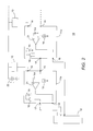
- FIG. 3 schematically illustrates an embodiment of a sequencing system 10 .
- Each IC may have an input 17 , and a sequence output 15 .
- the ICs may be connected in a daisy chain, wherein the output of a first IC is electrically connected to the input of a second IC.
- the output of the first IC 11 a may be electrically connected to the input of the second IC 11 b
- the output of the second IC 11 b may be electrically connected to the input of a third IC 11 c , and so on.
- Each IC may also have a load output 14 , which may be electrically connected to a load 13 .
- the load 13 may comprise an LED load.
- the LED load may contain one or more LEDs.
- the sequencing system 10 may also have a control unit 12 .
- the control unit 12 may be a microprocessor and may also serve as a voltage source.
- the control unit 12 may be coupled to a first integrated circuit 11 a of the plurality of ICs.
- the control unit 12 may provide on/off control.
- the system of FIG. 3 illustrates a sequencing system 10 having three (3) ICs, however it is understood that the system may contain any number of ICs.
- Each IC 11 a , 11 b , 11 c may have a diagnostic circuit.
- the diagnostic circuit may detect an open circuit condition when the intermediate communication signal coupling two ICs is broken.
- the diagnostic circuit may also detect an open circuit condition if there is open load.
- the diagnostic circuit may comprise a pull-up component 18 , an open circuit detection component 21 , a first pull-down component 19 , a second pull-down component 23 , a fault switch 24 , and a reference voltage Vol.
- the first pull-down component 19 may be a current source
- the open circuit detection component 21 may be a comparator
- the pull-up component 18 may be a resistor. According to the present embodiment in FIG. 3 , pull-up component 18 is shown as a current source.
- the last circuit in the chain may have a separate pull-up component (not shown).
- a separate pull-up component For example, during normal operation (i.e. an open circuit condition is not present), the load connected to each IC is turned off.
- the pull-up components 18 of the first IC 11 a , the second IC 11 b , and third IC 11 c provide high voltages at nodes 17 .
- the high voltage at node 17 also corresponds to a high voltage at node 15 .
- the voltage at node 15 is compared to the reference voltage Vol through the open circuit detection component 21 . If there is a positive difference or no difference between the voltage at node 15 and the reference voltage Vol, the output of open circuit detection component 21 will not signal an open circuit condition, thereby leaving the fault switch 24 open.
- the pull-down component 19 of the second IC 11 b will become dominant since the pull-up component 18 of the third IC 11 c is no longer influencing the voltage at node 15 of the second IC 11 b , thereby causing the voltage at node 15 of the second IC 11 b to fall to a value less than the reference voltage Vol.
- the open circuit detection component 21 will now detect a negative difference in the voltage between node 15 of the second IC 11 b and the reference voltage Vol. This difference in voltage levels will be interpreted as an open circuit condition. This open circuit condition causes the LED load of the second IC 11 b to be turned off.
- An open circuit signal is then sent to the fault switch 24 of the second IC 11 b .
- the fault switch 24 of the second IC 11 b receives the open circuit signal, the fault switch 24 closes, thereby turning on the second pull-down component 23 of the second IC 11 b . Since the second pull-down component 23 is much greater than the pull-up component 18 , the voltage at node 17 of the second IC 11 b and the voltage at node 15 of the first IC 11 a are lowered to a value less than Vol. Therefore, since the voltage at node 15 of the first IC is lower than the reference voltage Vol, the open circuit detection component 21 will now detect a negative difference in the voltage between node 15 of the first IC 11 a and the reference voltage Vol.
- This difference in voltage levels will be interpreted as an open circuit condition.
- the open circuit condition causes the LED load of the first IC 11 a to be turned off.
- An open circuit signal is then sent to the fault switch 24 of the first IC 11 a .
- the fault switch 24 of the first IC 11 a receives the open circuit signal, the fault switch 24 closes, thereby turning on the second pull-down component 23 of the first IC 11 a . Since the second pull-down component 23 is much greater than the pull-up component 18 , the voltage at node 17 of the first IC 11 a is lowered.
- the voltage at node 17 of first IC 11 a is reported to the control unit 12 through the diagnostic reporting input 27 , where a low voltage at node 17 is interpreted as an open circuit condition.
- the diagnostic circuit or a separate OLDC may also detect an open circuit condition if there is open load, which may be caused by a broken connection between the load output 14 and the load 13 .
- the load 13 may be electrically connected to an OLDC.
- the OLDC may measure the current through the load 13 , and could be electrically connected to the fault switch 24 .
- the OLDC is not shown, however, according to at least one embodiment, the OLDC may be substantially similar to and implemented in substantially the same way as the diagnostic circuit described above.
- voltage source(s) 22 may function in a similar way to voltage source Vreg
- load 13 may function in a similar way to pull-up component 18
- additional circuitry within the ICs 11 a , 11 b , and 11 c which are similar to the diagnostic circuit described above may be implemented.
- an open load signal could be sent to the fault switch 24 of the second IC 11 b .
- the fault switch 24 of the second IC 11 b receives the open load signal, the fault switch 24 closes, thereby turning on the second pull-down component 23 of the second IC 11 b .
- the open circuit detection component 21 will now detect a negative difference in the voltage between node 15 of the first IC 11 a and the reference voltage Vol. This difference in voltage levels will be interpreted as an open circuit condition. An open circuit signal is then sent to the fault switch 24 of the first IC 11 a .
- the fault switch 24 of the first IC 11 a When the fault switch 24 of the first IC 11 a receives the open circuit signal, the fault switch 24 closes, thereby turning on the second pull-down component 23 of the first IC 11 a . Since the second pull-down component 23 is much greater than the pull-up component 18 , the voltage at node 17 of the first IC 11 a is lowered. The voltage at node 17 of first IC 11 a is reported to the control unit 12 through the diagnostic reporting input 27 , where a low voltage at node 17 is interpreted as an open circuit condition.
- the sequencing system 10 may be reset by using a clear switch 25 connected to Vcc.
- the clear switch 25 may be connected to the control unit 12 through a separate pin, or may be connected to another system device which is connected to Vcc.
- a novel system is disclosed. Included in one embodiment, among other features, is a diagnostic reporting circuit that detects an open circuit condition. The system ensures that if an open circuit condition is detected, all loads are turned off.
- inventive aspects may lie in less than all features of a single foregoing disclosed embodiment.
- inventive aspects may lie in less than all features of a single foregoing disclosed embodiment.
- the hereinafter expressed claims are hereby expressly incorporated into this Detailed Description of the Drawings, with each claim standing on its own as a separate embodiment of the invention.
- some embodiments described herein include some but not other features included in other embodiments, combinations of features of different embodiments are meant to be within the scope of the invention, and form different embodiments, as would be understood by those skilled in the art.
Landscapes
- Circuit Arrangement For Electric Light Sources In General (AREA)
- Testing Of Short-Circuits, Discontinuities, Leakage, Or Incorrect Line Connections (AREA)
- Physics & Mathematics (AREA)
- General Physics & Mathematics (AREA)
Abstract
Description
Claims (17)
Priority Applications (2)
| Application Number | Priority Date | Filing Date | Title |
|---|---|---|---|
| US14/804,166 US9913355B2 (en) | 2014-07-30 | 2015-07-20 | Method of forming a sequencing system and structure therefor |
| CN201520558334.0U CN204836686U (en) | 2014-07-30 | 2015-07-29 | Sequencing luminescent system and open -circuit detecting system |
Applications Claiming Priority (2)
| Application Number | Priority Date | Filing Date | Title |
|---|---|---|---|
| US201462031060P | 2014-07-30 | 2014-07-30 | |
| US14/804,166 US9913355B2 (en) | 2014-07-30 | 2015-07-20 | Method of forming a sequencing system and structure therefor |
Publications (2)
| Publication Number | Publication Date |
|---|---|
| US20160033584A1 US20160033584A1 (en) | 2016-02-04 |
| US9913355B2 true US9913355B2 (en) | 2018-03-06 |
Family
ID=55179790
Family Applications (1)
| Application Number | Title | Priority Date | Filing Date |
|---|---|---|---|
| US14/804,166 Active 2036-08-18 US9913355B2 (en) | 2014-07-30 | 2015-07-20 | Method of forming a sequencing system and structure therefor |
Country Status (1)
| Country | Link |
|---|---|
| US (1) | US9913355B2 (en) |
Families Citing this family (3)
| Publication number | Priority date | Publication date | Assignee | Title |
|---|---|---|---|---|
| US10725097B2 (en) * | 2016-12-20 | 2020-07-28 | Intel Corporation | Platform component interconnect testing |
| TWI700963B (en) | 2019-08-28 | 2020-08-01 | 群光電能科技股份有限公司 | Control apparatus for light emitting diode |
| CN114465532B (en) * | 2020-11-06 | 2023-08-11 | 致新科技股份有限公司 | Motor controller |
Citations (7)
| Publication number | Priority date | Publication date | Assignee | Title |
|---|---|---|---|---|
| US5232243A (en) * | 1991-04-09 | 1993-08-03 | Trw Vehicle Safety Systems Inc. | Occupant sensing apparatus |
| US20060117232A1 (en) * | 2004-10-28 | 2006-06-01 | Seagate Technology Llc | Testing device and method for an integrated circuit |
| US20060208755A1 (en) * | 2000-02-23 | 2006-09-21 | Bjork Russell S | In-tray burn-in board, device and test assembly for testing integrated circuit devices in situ on processing trays |
| US7911220B2 (en) * | 2003-08-27 | 2011-03-22 | Nec Corporation | Semiconductor integrated circuit apparatus, measurement result management system, and management server |
| US8035409B2 (en) * | 2009-04-29 | 2011-10-11 | International Business Machines Corporation | System and method implementing short-pulse propagation technique on production-level boards with incremental accuracy and productivity levels |
| US20140164858A1 (en) * | 2012-12-06 | 2014-06-12 | Wistron Corporation | Testing apparatus and testing method of electronic device |
| US20140266749A1 (en) * | 2013-03-15 | 2014-09-18 | Lockheed Martin Corporation | Printed light-emitting diode circuit for item validation |
-
2015
- 2015-07-20 US US14/804,166 patent/US9913355B2/en active Active
Patent Citations (7)
| Publication number | Priority date | Publication date | Assignee | Title |
|---|---|---|---|---|
| US5232243A (en) * | 1991-04-09 | 1993-08-03 | Trw Vehicle Safety Systems Inc. | Occupant sensing apparatus |
| US20060208755A1 (en) * | 2000-02-23 | 2006-09-21 | Bjork Russell S | In-tray burn-in board, device and test assembly for testing integrated circuit devices in situ on processing trays |
| US7911220B2 (en) * | 2003-08-27 | 2011-03-22 | Nec Corporation | Semiconductor integrated circuit apparatus, measurement result management system, and management server |
| US20060117232A1 (en) * | 2004-10-28 | 2006-06-01 | Seagate Technology Llc | Testing device and method for an integrated circuit |
| US8035409B2 (en) * | 2009-04-29 | 2011-10-11 | International Business Machines Corporation | System and method implementing short-pulse propagation technique on production-level boards with incremental accuracy and productivity levels |
| US20140164858A1 (en) * | 2012-12-06 | 2014-06-12 | Wistron Corporation | Testing apparatus and testing method of electronic device |
| US20140266749A1 (en) * | 2013-03-15 | 2014-09-18 | Lockheed Martin Corporation | Printed light-emitting diode circuit for item validation |
Also Published As
| Publication number | Publication date |
|---|---|
| US20160033584A1 (en) | 2016-02-04 |
Similar Documents
| Publication | Publication Date | Title |
|---|---|---|
| US10374593B2 (en) | Semiconductor device | |
| US7663323B2 (en) | Monitoring device for an array of electrical units | |
| US20120200296A1 (en) | Technique for identifying at least one faulty light emitting diode in multiple strings of light emitting diodes | |
| US8436664B2 (en) | Circuit and method for implementing power good and chip enable control by a multi-functional pin of an integrated circuit | |
| JP2014519013A (en) | Method for identifying defects in LED strings | |
| US20130106470A1 (en) | Control device | |
| US9913355B2 (en) | Method of forming a sequencing system and structure therefor | |
| JP2015115692A (en) | Semiconductor abnormality detection circuit | |
| CN109477862B (en) | Vehicle-mounted control device | |
| KR101773053B1 (en) | Battery-monitoring unit | |
| US9295124B2 (en) | System using shunt circuits to selectively bypass open loads | |
| US8400075B2 (en) | Illumination circuit having bypass circuit controllable according to voltage change of series circuit thereof | |
| US20130221978A1 (en) | Light Emitting Device Control Circuit and Short Detection Circuit Thereof | |
| US9739845B2 (en) | Method for testing a signal path | |
| CN100437133C (en) | Low voltage replacement function detecting circuit | |
| US10999909B2 (en) | LED lighting device, particularly for vehicles | |
| US20150346243A1 (en) | Current load detection device and current load detection method | |
| US9448578B1 (en) | Interface supply circuit | |
| CN110532207A (en) | Bus system and its detection method | |
| US20090278562A1 (en) | Test Device and Test Method for Semiconductor Device | |
| US7030639B2 (en) | Semiconductor apparatus including a switch element and resistance element connected in series | |
| US10241148B2 (en) | Virtual access of input/output (I/O) for test via an on-chip star network | |
| US20140347063A1 (en) | Fan test device | |
| US20050146320A1 (en) | Differential active load | |
| EP2939344B1 (en) | Automatic input impedance control |
Legal Events
| Date | Code | Title | Description |
|---|---|---|---|
| AS | Assignment |
Owner name: SEMICONDUCTOR COMPONENTS INDUSTRIES, LLC, ARIZONA Free format text: ASSIGNMENT OF ASSIGNORS INTEREST;ASSIGNORS:KOLANKO, FRANK;VERMEIR, SAM;VAN DE MAELE, WIM;AND OTHERS;SIGNING DATES FROM 20150727 TO 20150811;REEL/FRAME:036319/0173 |
|
| AS | Assignment |
Owner name: DEUTSCHE BANK AG NEW YORK BRANCH, NEW YORK Free format text: SECURITY INTEREST;ASSIGNOR:SEMICONDUCTOR COMPONENTS INDUSTRIES, LLC;REEL/FRAME:038620/0087 Effective date: 20160415 |
|
| AS | Assignment |
Owner name: SEMICONDUCTOR COMPONENTS INDUSTRIES, LLC, ARIZONA Free format text: ASSIGNMENT OF ASSIGNORS INTEREST;ASSIGNOR:BLACKBURN, BRIAN K.;REEL/FRAME:038933/0949 Effective date: 20050207 |
|
| AS | Assignment |
Owner name: DEUTSCHE BANK AG NEW YORK BRANCH, AS COLLATERAL AG Free format text: CORRECTIVE ASSIGNMENT TO CORRECT THE INCORRECT PATENT NUMBER 5859768 AND TO RECITE COLLATERAL AGENT ROLE OF RECEIVING PARTY IN THE SECURITY INTEREST PREVIOUSLY RECORDED ON REEL 038620 FRAME 0087. ASSIGNOR(S) HEREBY CONFIRMS THE SECURITY INTEREST;ASSIGNOR:SEMICONDUCTOR COMPONENTS INDUSTRIES, LLC;REEL/FRAME:039853/0001 Effective date: 20160415 Owner name: DEUTSCHE BANK AG NEW YORK BRANCH, AS COLLATERAL AGENT, NEW YORK Free format text: CORRECTIVE ASSIGNMENT TO CORRECT THE INCORRECT PATENT NUMBER 5859768 AND TO RECITE COLLATERAL AGENT ROLE OF RECEIVING PARTY IN THE SECURITY INTEREST PREVIOUSLY RECORDED ON REEL 038620 FRAME 0087. ASSIGNOR(S) HEREBY CONFIRMS THE SECURITY INTEREST;ASSIGNOR:SEMICONDUCTOR COMPONENTS INDUSTRIES, LLC;REEL/FRAME:039853/0001 Effective date: 20160415 |
|
| STCF | Information on status: patent grant |
Free format text: PATENTED CASE |
|
| MAFP | Maintenance fee payment |
Free format text: PAYMENT OF MAINTENANCE FEE, 4TH YEAR, LARGE ENTITY (ORIGINAL EVENT CODE: M1551); ENTITY STATUS OF PATENT OWNER: LARGE ENTITY Year of fee payment: 4 |
|
| AS | Assignment |
Owner name: FAIRCHILD SEMICONDUCTOR CORPORATION, ARIZONA Free format text: RELEASE OF SECURITY INTEREST IN PATENTS RECORDED AT REEL 038620, FRAME 0087;ASSIGNOR:DEUTSCHE BANK AG NEW YORK BRANCH, AS COLLATERAL AGENT;REEL/FRAME:064070/0001 Effective date: 20230622 Owner name: SEMICONDUCTOR COMPONENTS INDUSTRIES, LLC, ARIZONA Free format text: RELEASE OF SECURITY INTEREST IN PATENTS RECORDED AT REEL 038620, FRAME 0087;ASSIGNOR:DEUTSCHE BANK AG NEW YORK BRANCH, AS COLLATERAL AGENT;REEL/FRAME:064070/0001 Effective date: 20230622 |