US9911784B2 - Monolithic visible-infrared focal plane array on silicon - Google Patents
Monolithic visible-infrared focal plane array on silicon Download PDFInfo
- Publication number
- US9911784B2 US9911784B2 US15/415,281 US201715415281A US9911784B2 US 9911784 B2 US9911784 B2 US 9911784B2 US 201715415281 A US201715415281 A US 201715415281A US 9911784 B2 US9911784 B2 US 9911784B2
- Authority
- US
- United States
- Prior art keywords
- layer
- germanium
- silicon substrate
- photodetector
- semiconductor material
- Prior art date
- Legal status (The legal status is an assumption and is not a legal conclusion. Google has not performed a legal analysis and makes no representation as to the accuracy of the status listed.)
- Active
Links
- 229910052710 silicon Inorganic materials 0.000 title claims abstract description 57
- 239000010703 silicon Substances 0.000 title claims abstract description 56
- 230000005855 radiation Effects 0.000 claims abstract description 77
- 239000000758 substrate Substances 0.000 claims abstract description 77
- XUIMIQQOPSSXEZ-UHFFFAOYSA-N Silicon Chemical compound [Si] XUIMIQQOPSSXEZ-UHFFFAOYSA-N 0.000 claims abstract description 55
- 239000000463 material Substances 0.000 claims abstract description 41
- 239000004065 semiconductor Substances 0.000 claims abstract description 39
- 229910052732 germanium Inorganic materials 0.000 claims abstract description 35
- GNPVGFCGXDBREM-UHFFFAOYSA-N germanium atom Chemical compound [Ge] GNPVGFCGXDBREM-UHFFFAOYSA-N 0.000 claims abstract description 34
- 238000000034 method Methods 0.000 claims abstract description 32
- FVBUAEGBCNSCDD-UHFFFAOYSA-N silicide(4-) Chemical compound [Si-4] FVBUAEGBCNSCDD-UHFFFAOYSA-N 0.000 description 48
- JBRZTFJDHDCESZ-UHFFFAOYSA-N AsGa Chemical compound [As]#[Ga] JBRZTFJDHDCESZ-UHFFFAOYSA-N 0.000 description 35
- 229910000530 Gallium indium arsenide Inorganic materials 0.000 description 20
- 229910001218 Gallium arsenide Inorganic materials 0.000 description 18
- 238000000151 deposition Methods 0.000 description 18
- 230000008021 deposition Effects 0.000 description 15
- 239000002019 doping agent Substances 0.000 description 15
- 238000004519 manufacturing process Methods 0.000 description 12
- 239000000203 mixture Substances 0.000 description 9
- 230000015572 biosynthetic process Effects 0.000 description 8
- 238000005530 etching Methods 0.000 description 8
- VYPSYNLAJGMNEJ-UHFFFAOYSA-N Silicium dioxide Chemical compound O=[Si]=O VYPSYNLAJGMNEJ-UHFFFAOYSA-N 0.000 description 7
- 229910052751 metal Inorganic materials 0.000 description 6
- 239000002184 metal Substances 0.000 description 6
- 229910021332 silicide Inorganic materials 0.000 description 5
- 238000005137 deposition process Methods 0.000 description 4
- 239000012212 insulator Substances 0.000 description 4
- 238000012986 modification Methods 0.000 description 4
- 230000004048 modification Effects 0.000 description 4
- 229910005542 GaSb Inorganic materials 0.000 description 3
- 239000013078 crystal Substances 0.000 description 3
- 238000003384 imaging method Methods 0.000 description 3
- 230000001681 protective effect Effects 0.000 description 3
- 239000000377 silicon dioxide Substances 0.000 description 3
- ZOXJGFHDIHLPTG-UHFFFAOYSA-N Boron Chemical compound [B] ZOXJGFHDIHLPTG-UHFFFAOYSA-N 0.000 description 2
- 229910000661 Mercury cadmium telluride Inorganic materials 0.000 description 2
- 229910052782 aluminium Inorganic materials 0.000 description 2
- 229910052785 arsenic Inorganic materials 0.000 description 2
- RQNWIZPPADIBDY-UHFFFAOYSA-N arsenic atom Chemical compound [As] RQNWIZPPADIBDY-UHFFFAOYSA-N 0.000 description 2
- 238000001505 atmospheric-pressure chemical vapour deposition Methods 0.000 description 2
- 229910052796 boron Inorganic materials 0.000 description 2
- 238000005229 chemical vapour deposition Methods 0.000 description 2
- 229910052681 coesite Inorganic materials 0.000 description 2
- 229910052802 copper Inorganic materials 0.000 description 2
- 229910052906 cristobalite Inorganic materials 0.000 description 2
- 239000003989 dielectric material Substances 0.000 description 2
- 238000005516 engineering process Methods 0.000 description 2
- 229910052737 gold Inorganic materials 0.000 description 2
- 238000005286 illumination Methods 0.000 description 2
- RPQDHPTXJYYUPQ-UHFFFAOYSA-N indium arsenide Chemical class [In]#[As] RPQDHPTXJYYUPQ-UHFFFAOYSA-N 0.000 description 2
- 239000002096 quantum dot Substances 0.000 description 2
- 238000001289 rapid thermal chemical vapour deposition Methods 0.000 description 2
- 229910052682 stishovite Inorganic materials 0.000 description 2
- 229910052905 tridymite Inorganic materials 0.000 description 2
- 238000000038 ultrahigh vacuum chemical vapour deposition Methods 0.000 description 2
- 229910000673 Indium arsenide Inorganic materials 0.000 description 1
- 229910052581 Si3N4 Inorganic materials 0.000 description 1
- 238000010521 absorption reaction Methods 0.000 description 1
- 230000006978 adaptation Effects 0.000 description 1
- 238000003491 array Methods 0.000 description 1
- 239000004020 conductor Substances 0.000 description 1
- 239000000470 constituent Substances 0.000 description 1
- 238000005336 cracking Methods 0.000 description 1
- 230000007547 defect Effects 0.000 description 1
- 239000007789 gas Substances 0.000 description 1
- 230000010354 integration Effects 0.000 description 1
- 230000000873 masking effect Effects 0.000 description 1
- 150000002739 metals Chemical class 0.000 description 1
- 238000004476 mid-IR spectroscopy Methods 0.000 description 1
- 238000001451 molecular beam epitaxy Methods 0.000 description 1
- 230000004297 night vision Effects 0.000 description 1
- 238000000059 patterning Methods 0.000 description 1
- 239000000376 reactant Substances 0.000 description 1
- 238000013341 scale-up Methods 0.000 description 1
- 235000012239 silicon dioxide Nutrition 0.000 description 1
- HQVNEWCFYHHQES-UHFFFAOYSA-N silicon nitride Chemical compound N12[Si]34N5[Si]62N3[Si]51N64 HQVNEWCFYHHQES-UHFFFAOYSA-N 0.000 description 1
- 229910052814 silicon oxide Inorganic materials 0.000 description 1
- 239000000126 substance Substances 0.000 description 1
- 229910052720 vanadium Inorganic materials 0.000 description 1
Images


Classifications
-
- H—ELECTRICITY
- H01—ELECTRIC ELEMENTS
- H01L—SEMICONDUCTOR DEVICES NOT COVERED BY CLASS H10
- H01L27/00—Devices consisting of a plurality of semiconductor or other solid-state components formed in or on a common substrate
- H01L27/14—Devices consisting of a plurality of semiconductor or other solid-state components formed in or on a common substrate including semiconductor components sensitive to infrared radiation, light, electromagnetic radiation of shorter wavelength or corpuscular radiation and specially adapted either for the conversion of the energy of such radiation into electrical energy or for the control of electrical energy by such radiation
- H01L27/144—Devices controlled by radiation
- H01L27/146—Imager structures
- H01L27/14643—Photodiode arrays; MOS imagers
- H01L27/14649—Infrared imagers
- H01L27/14652—Multispectral infrared imagers, having a stacked pixel-element structure, e.g. npn, npnpn or MQW structures
-
- H—ELECTRICITY
- H01—ELECTRIC ELEMENTS
- H01L—SEMICONDUCTOR DEVICES NOT COVERED BY CLASS H10
- H01L27/00—Devices consisting of a plurality of semiconductor or other solid-state components formed in or on a common substrate
- H01L27/14—Devices consisting of a plurality of semiconductor or other solid-state components formed in or on a common substrate including semiconductor components sensitive to infrared radiation, light, electromagnetic radiation of shorter wavelength or corpuscular radiation and specially adapted either for the conversion of the energy of such radiation into electrical energy or for the control of electrical energy by such radiation
- H01L27/144—Devices controlled by radiation
- H01L27/1443—Devices controlled by radiation with at least one potential jump or surface barrier
-
- H—ELECTRICITY
- H01—ELECTRIC ELEMENTS
- H01L—SEMICONDUCTOR DEVICES NOT COVERED BY CLASS H10
- H01L27/00—Devices consisting of a plurality of semiconductor or other solid-state components formed in or on a common substrate
- H01L27/14—Devices consisting of a plurality of semiconductor or other solid-state components formed in or on a common substrate including semiconductor components sensitive to infrared radiation, light, electromagnetic radiation of shorter wavelength or corpuscular radiation and specially adapted either for the conversion of the energy of such radiation into electrical energy or for the control of electrical energy by such radiation
- H01L27/144—Devices controlled by radiation
- H01L27/146—Imager structures
- H01L27/14601—Structural or functional details thereof
- H01L27/14634—Assemblies, i.e. Hybrid structures
-
- H—ELECTRICITY
- H01—ELECTRIC ELEMENTS
- H01L—SEMICONDUCTOR DEVICES NOT COVERED BY CLASS H10
- H01L27/00—Devices consisting of a plurality of semiconductor or other solid-state components formed in or on a common substrate
- H01L27/14—Devices consisting of a plurality of semiconductor or other solid-state components formed in or on a common substrate including semiconductor components sensitive to infrared radiation, light, electromagnetic radiation of shorter wavelength or corpuscular radiation and specially adapted either for the conversion of the energy of such radiation into electrical energy or for the control of electrical energy by such radiation
- H01L27/144—Devices controlled by radiation
- H01L27/146—Imager structures
- H01L27/14601—Structural or functional details thereof
- H01L27/14636—Interconnect structures
-
- H—ELECTRICITY
- H01—ELECTRIC ELEMENTS
- H01L—SEMICONDUCTOR DEVICES NOT COVERED BY CLASS H10
- H01L27/00—Devices consisting of a plurality of semiconductor or other solid-state components formed in or on a common substrate
- H01L27/14—Devices consisting of a plurality of semiconductor or other solid-state components formed in or on a common substrate including semiconductor components sensitive to infrared radiation, light, electromagnetic radiation of shorter wavelength or corpuscular radiation and specially adapted either for the conversion of the energy of such radiation into electrical energy or for the control of electrical energy by such radiation
- H01L27/144—Devices controlled by radiation
- H01L27/146—Imager structures
- H01L27/14601—Structural or functional details thereof
- H01L27/1464—Back illuminated imager structures
-
- H—ELECTRICITY
- H01—ELECTRIC ELEMENTS
- H01L—SEMICONDUCTOR DEVICES NOT COVERED BY CLASS H10
- H01L27/00—Devices consisting of a plurality of semiconductor or other solid-state components formed in or on a common substrate
- H01L27/14—Devices consisting of a plurality of semiconductor or other solid-state components formed in or on a common substrate including semiconductor components sensitive to infrared radiation, light, electromagnetic radiation of shorter wavelength or corpuscular radiation and specially adapted either for the conversion of the energy of such radiation into electrical energy or for the control of electrical energy by such radiation
- H01L27/144—Devices controlled by radiation
- H01L27/146—Imager structures
- H01L27/14643—Photodiode arrays; MOS imagers
- H01L27/14645—Colour imagers
- H01L27/14647—Multicolour imagers having a stacked pixel-element structure, e.g. npn, npnpn or MQW elements
-
- H—ELECTRICITY
- H01—ELECTRIC ELEMENTS
- H01L—SEMICONDUCTOR DEVICES NOT COVERED BY CLASS H10
- H01L27/00—Devices consisting of a plurality of semiconductor or other solid-state components formed in or on a common substrate
- H01L27/14—Devices consisting of a plurality of semiconductor or other solid-state components formed in or on a common substrate including semiconductor components sensitive to infrared radiation, light, electromagnetic radiation of shorter wavelength or corpuscular radiation and specially adapted either for the conversion of the energy of such radiation into electrical energy or for the control of electrical energy by such radiation
- H01L27/144—Devices controlled by radiation
- H01L27/146—Imager structures
- H01L27/14643—Photodiode arrays; MOS imagers
- H01L27/14649—Infrared imagers
- H01L27/1465—Infrared imagers of the hybrid type
-
- H—ELECTRICITY
- H01—ELECTRIC ELEMENTS
- H01L—SEMICONDUCTOR DEVICES NOT COVERED BY CLASS H10
- H01L27/00—Devices consisting of a plurality of semiconductor or other solid-state components formed in or on a common substrate
- H01L27/14—Devices consisting of a plurality of semiconductor or other solid-state components formed in or on a common substrate including semiconductor components sensitive to infrared radiation, light, electromagnetic radiation of shorter wavelength or corpuscular radiation and specially adapted either for the conversion of the energy of such radiation into electrical energy or for the control of electrical energy by such radiation
- H01L27/144—Devices controlled by radiation
- H01L27/146—Imager structures
- H01L27/14683—Processes or apparatus peculiar to the manufacture or treatment of these devices or parts thereof
- H01L27/14689—MOS based technologies
-
- H—ELECTRICITY
- H01—ELECTRIC ELEMENTS
- H01L—SEMICONDUCTOR DEVICES NOT COVERED BY CLASS H10
- H01L27/00—Devices consisting of a plurality of semiconductor or other solid-state components formed in or on a common substrate
- H01L27/14—Devices consisting of a plurality of semiconductor or other solid-state components formed in or on a common substrate including semiconductor components sensitive to infrared radiation, light, electromagnetic radiation of shorter wavelength or corpuscular radiation and specially adapted either for the conversion of the energy of such radiation into electrical energy or for the control of electrical energy by such radiation
- H01L27/144—Devices controlled by radiation
- H01L27/146—Imager structures
- H01L27/14683—Processes or apparatus peculiar to the manufacture or treatment of these devices or parts thereof
- H01L27/1469—Assemblies, i.e. hybrid integration
-
- H—ELECTRICITY
- H01—ELECTRIC ELEMENTS
- H01L—SEMICONDUCTOR DEVICES NOT COVERED BY CLASS H10
- H01L27/00—Devices consisting of a plurality of semiconductor or other solid-state components formed in or on a common substrate
- H01L27/14—Devices consisting of a plurality of semiconductor or other solid-state components formed in or on a common substrate including semiconductor components sensitive to infrared radiation, light, electromagnetic radiation of shorter wavelength or corpuscular radiation and specially adapted either for the conversion of the energy of such radiation into electrical energy or for the control of electrical energy by such radiation
- H01L27/144—Devices controlled by radiation
- H01L27/146—Imager structures
- H01L27/14683—Processes or apparatus peculiar to the manufacture or treatment of these devices or parts thereof
- H01L27/14694—The active layers comprising only AIIIBV compounds, e.g. GaAs, InP
-
- H—ELECTRICITY
- H01—ELECTRIC ELEMENTS
- H01L—SEMICONDUCTOR DEVICES NOT COVERED BY CLASS H10
- H01L31/00—Semiconductor devices sensitive to infrared radiation, light, electromagnetic radiation of shorter wavelength or corpuscular radiation and specially adapted either for the conversion of the energy of such radiation into electrical energy or for the control of electrical energy by such radiation; Processes or apparatus specially adapted for the manufacture or treatment thereof or of parts thereof; Details thereof
- H01L31/0248—Semiconductor devices sensitive to infrared radiation, light, electromagnetic radiation of shorter wavelength or corpuscular radiation and specially adapted either for the conversion of the energy of such radiation into electrical energy or for the control of electrical energy by such radiation; Processes or apparatus specially adapted for the manufacture or treatment thereof or of parts thereof; Details thereof characterised by their semiconductor bodies
- H01L31/0256—Semiconductor devices sensitive to infrared radiation, light, electromagnetic radiation of shorter wavelength or corpuscular radiation and specially adapted either for the conversion of the energy of such radiation into electrical energy or for the control of electrical energy by such radiation; Processes or apparatus specially adapted for the manufacture or treatment thereof or of parts thereof; Details thereof characterised by their semiconductor bodies characterised by the material
- H01L31/0264—Inorganic materials
- H01L31/028—Inorganic materials including, apart from doping material or other impurities, only elements of Group IV of the Periodic System
-
- H—ELECTRICITY
- H01—ELECTRIC ELEMENTS
- H01L—SEMICONDUCTOR DEVICES NOT COVERED BY CLASS H10
- H01L31/00—Semiconductor devices sensitive to infrared radiation, light, electromagnetic radiation of shorter wavelength or corpuscular radiation and specially adapted either for the conversion of the energy of such radiation into electrical energy or for the control of electrical energy by such radiation; Processes or apparatus specially adapted for the manufacture or treatment thereof or of parts thereof; Details thereof
- H01L31/0248—Semiconductor devices sensitive to infrared radiation, light, electromagnetic radiation of shorter wavelength or corpuscular radiation and specially adapted either for the conversion of the energy of such radiation into electrical energy or for the control of electrical energy by such radiation; Processes or apparatus specially adapted for the manufacture or treatment thereof or of parts thereof; Details thereof characterised by their semiconductor bodies
- H01L31/0256—Semiconductor devices sensitive to infrared radiation, light, electromagnetic radiation of shorter wavelength or corpuscular radiation and specially adapted either for the conversion of the energy of such radiation into electrical energy or for the control of electrical energy by such radiation; Processes or apparatus specially adapted for the manufacture or treatment thereof or of parts thereof; Details thereof characterised by their semiconductor bodies characterised by the material
- H01L31/0264—Inorganic materials
- H01L31/0304—Inorganic materials including, apart from doping materials or other impurities, only AIIIBV compounds
- H01L31/03046—Inorganic materials including, apart from doping materials or other impurities, only AIIIBV compounds including ternary or quaternary compounds, e.g. GaAlAs, InGaAs, InGaAsP
-
- H—ELECTRICITY
- H01—ELECTRIC ELEMENTS
- H01L—SEMICONDUCTOR DEVICES NOT COVERED BY CLASS H10
- H01L31/00—Semiconductor devices sensitive to infrared radiation, light, electromagnetic radiation of shorter wavelength or corpuscular radiation and specially adapted either for the conversion of the energy of such radiation into electrical energy or for the control of electrical energy by such radiation; Processes or apparatus specially adapted for the manufacture or treatment thereof or of parts thereof; Details thereof
- H01L31/0248—Semiconductor devices sensitive to infrared radiation, light, electromagnetic radiation of shorter wavelength or corpuscular radiation and specially adapted either for the conversion of the energy of such radiation into electrical energy or for the control of electrical energy by such radiation; Processes or apparatus specially adapted for the manufacture or treatment thereof or of parts thereof; Details thereof characterised by their semiconductor bodies
- H01L31/0352—Semiconductor devices sensitive to infrared radiation, light, electromagnetic radiation of shorter wavelength or corpuscular radiation and specially adapted either for the conversion of the energy of such radiation into electrical energy or for the control of electrical energy by such radiation; Processes or apparatus specially adapted for the manufacture or treatment thereof or of parts thereof; Details thereof characterised by their semiconductor bodies characterised by their shape or by the shapes, relative sizes or disposition of the semiconductor regions
- H01L31/035209—Semiconductor devices sensitive to infrared radiation, light, electromagnetic radiation of shorter wavelength or corpuscular radiation and specially adapted either for the conversion of the energy of such radiation into electrical energy or for the control of electrical energy by such radiation; Processes or apparatus specially adapted for the manufacture or treatment thereof or of parts thereof; Details thereof characterised by their semiconductor bodies characterised by their shape or by the shapes, relative sizes or disposition of the semiconductor regions comprising a quantum structures
- H01L31/035218—Semiconductor devices sensitive to infrared radiation, light, electromagnetic radiation of shorter wavelength or corpuscular radiation and specially adapted either for the conversion of the energy of such radiation into electrical energy or for the control of electrical energy by such radiation; Processes or apparatus specially adapted for the manufacture or treatment thereof or of parts thereof; Details thereof characterised by their semiconductor bodies characterised by their shape or by the shapes, relative sizes or disposition of the semiconductor regions comprising a quantum structures the quantum structure being quantum dots
-
- H—ELECTRICITY
- H01—ELECTRIC ELEMENTS
- H01L—SEMICONDUCTOR DEVICES NOT COVERED BY CLASS H10
- H01L31/00—Semiconductor devices sensitive to infrared radiation, light, electromagnetic radiation of shorter wavelength or corpuscular radiation and specially adapted either for the conversion of the energy of such radiation into electrical energy or for the control of electrical energy by such radiation; Processes or apparatus specially adapted for the manufacture or treatment thereof or of parts thereof; Details thereof
- H01L31/08—Semiconductor devices sensitive to infrared radiation, light, electromagnetic radiation of shorter wavelength or corpuscular radiation and specially adapted either for the conversion of the energy of such radiation into electrical energy or for the control of electrical energy by such radiation; Processes or apparatus specially adapted for the manufacture or treatment thereof or of parts thereof; Details thereof in which radiation controls flow of current through the device, e.g. photoresistors
- H01L31/10—Semiconductor devices sensitive to infrared radiation, light, electromagnetic radiation of shorter wavelength or corpuscular radiation and specially adapted either for the conversion of the energy of such radiation into electrical energy or for the control of electrical energy by such radiation; Processes or apparatus specially adapted for the manufacture or treatment thereof or of parts thereof; Details thereof in which radiation controls flow of current through the device, e.g. photoresistors characterised by at least one potential-jump barrier or surface barrier, e.g. phototransistors
- H01L31/101—Devices sensitive to infrared, visible or ultraviolet radiation
- H01L31/102—Devices sensitive to infrared, visible or ultraviolet radiation characterised by only one potential barrier or surface barrier
- H01L31/105—Devices sensitive to infrared, visible or ultraviolet radiation characterised by only one potential barrier or surface barrier the potential barrier being of the PIN type
-
- H—ELECTRICITY
- H01—ELECTRIC ELEMENTS
- H01L—SEMICONDUCTOR DEVICES NOT COVERED BY CLASS H10
- H01L31/00—Semiconductor devices sensitive to infrared radiation, light, electromagnetic radiation of shorter wavelength or corpuscular radiation and specially adapted either for the conversion of the energy of such radiation into electrical energy or for the control of electrical energy by such radiation; Processes or apparatus specially adapted for the manufacture or treatment thereof or of parts thereof; Details thereof
- H01L31/18—Processes or apparatus specially adapted for the manufacture or treatment of these devices or of parts thereof
- H01L31/1804—Processes or apparatus specially adapted for the manufacture or treatment of these devices or of parts thereof comprising only elements of Group IV of the Periodic System
- H01L31/1808—Processes or apparatus specially adapted for the manufacture or treatment of these devices or of parts thereof comprising only elements of Group IV of the Periodic System including only Ge
-
- H—ELECTRICITY
- H01—ELECTRIC ELEMENTS
- H01L—SEMICONDUCTOR DEVICES NOT COVERED BY CLASS H10
- H01L31/00—Semiconductor devices sensitive to infrared radiation, light, electromagnetic radiation of shorter wavelength or corpuscular radiation and specially adapted either for the conversion of the energy of such radiation into electrical energy or for the control of electrical energy by such radiation; Processes or apparatus specially adapted for the manufacture or treatment thereof or of parts thereof; Details thereof
- H01L31/18—Processes or apparatus specially adapted for the manufacture or treatment of these devices or of parts thereof
- H01L31/184—Processes or apparatus specially adapted for the manufacture or treatment of these devices or of parts thereof the active layers comprising only AIIIBV compounds, e.g. GaAs, InP
- H01L31/1844—Processes or apparatus specially adapted for the manufacture or treatment of these devices or of parts thereof the active layers comprising only AIIIBV compounds, e.g. GaAs, InP comprising ternary or quaternary compounds, e.g. Ga Al As, In Ga As P
Landscapes
- Engineering & Computer Science (AREA)
- Physics & Mathematics (AREA)
- Power Engineering (AREA)
- Electromagnetism (AREA)
- Condensed Matter Physics & Semiconductors (AREA)
- General Physics & Mathematics (AREA)
- Computer Hardware Design (AREA)
- Microelectronics & Electronic Packaging (AREA)
- Chemical & Material Sciences (AREA)
- Inorganic Chemistry (AREA)
- Manufacturing & Machinery (AREA)
- Spectroscopy & Molecular Physics (AREA)
- Solid State Image Pick-Up Elements (AREA)
- Light Receiving Elements (AREA)
Abstract
A structure includes a silicon substrate; silicon readout circuitry disposed on a first portion of a top surface of the substrate and a radiation detecting pixel disposed on a second portion of the top surface of the substrate. The pixel has a plurality of radiation detectors connected with the readout circuitry. The plurality of radiation detectors are composed of at least one visible wavelength radiation detector containing germanium and at least one infrared wavelength radiation detector containing a Group III-V semiconductor material. A method includes providing a silicon substrate; forming silicon readout circuitry on a first portion of a top surface of the substrate and forming a radiation detecting pixel, on a second portion of the top surface of the substrate, that has a plurality of radiation detectors formed to contain a visible wavelength detector composed of germanium and an infrared wavelength detector composed of a Group III-V semiconductor material.
Description
This patent application is a continuation patent application of copending U.S. patent application Ser. No. 15/196,307, filed Jun. 29, 2016, which is a divisional patent application of U.S. patent application Ser. No. 14/744,210, filed Jun. 19, 2015, now U.S. Pat. No. 9,472,588, the disclosures of which are incorporated by reference herein in their entireties.
The various embodiments of this invention relate generally to semiconductor devices and fabrication techniques and, more specifically, relate to the fabrication of semiconductor detectors of electromagnetic (EM) radiation including EM radiation in the visible and the infrared (IR) wavelength bands.
Visible to IR responsive focal plane arrays (FPAs) have applications in night vision devices and various sensing and imaging applications. The current dominant technology uses Group II-VI semiconductor materials such as HgCdTe for detecting IR radiation. However, conventional HgCdTe detectors can exhibit manufacturing and performance issues including, for example, non-uniformity and a difficulty to scale up.
An aspect of the non-limiting embodiments of this invention is a structure that comprises a silicon substrate; silicon readout circuitry disposed on a first portion of a top surface of the silicon substrate; and a radiation detecting pixel disposed on a second portion of the top surface of the silicon substrate. The radiation detecting pixel is comprised of a plurality of radiation detectors connected with the silicon readout circuitry. In the structure the plurality of radiation detectors are comprised of at least one visible wavelength radiation detector comprised of germanium and at least one infrared wavelength radiation detector comprised of a Group III-V semiconductor material.
Another aspect of the non-limiting embodiments of this invention is a method that comprises providing a silicon substrate; forming silicon readout circuitry on a first portion of a top surface of the silicon substrate; and forming a radiation detecting pixel on a second portion of the top surface of the silicon substrate. The radiation detecting pixel is comprised of a plurality of radiation detectors connected with the silicon readout circuitry. The plurality of radiation detectors are formed to comprise at least one visible wavelength radiation detector comprised of germanium and at least one infrared wavelength radiation detector comprised of a Group III-V semiconductor material.
The word “exemplary” is used herein to mean “serving as an example, instance, or illustration.” Any embodiment described herein as “exemplary” is not necessarily to be construed as preferred or advantageous over other embodiments. All of the embodiments described in this Detailed Description are exemplary embodiments provided to enable persons skilled in the art to make or use the invention and not to limit the scope of the invention which is defined by the claims.
The terms “epitaxial growth and/or deposition” and “epitaxially formed and/or grown” mean the growth of a semiconductor material on a deposition surface of a semiconductor material, in which the semiconductor material being grown has the same crystalline characteristics as the semiconductor material of the deposition surface. In an epitaxial deposition process, the chemical reactants provided by source gases are controlled and the system parameters are set so that the depositing atoms arrive at the deposition surface of the semiconductor substrate with sufficient energy to move around on the surface and orient themselves to the crystal arrangement of the atoms of the deposition surface. Therefore, an epitaxial semiconductor material has the same crystalline characteristics as the deposition surface on which it is formed. For example, an epitaxial semiconductor material deposited on a {100} crystal surface will take on a {100} orientation. In some embodiments, epitaxial growth and/or deposition processes are selective to forming on semiconductor surface, and do not deposit material on dielectric surfaces, such as silicon dioxide or silicon nitride surfaces.
Examples of various epitaxial growth process apparatuses that are suitable for use in implementing the embodiments of this invention include, but are not limited to, rapid thermal chemical vapor deposition (RTCVD), low-energy plasma deposition (LEPD), ultra-high vacuum chemical vapor deposition (UHVCVD), atmospheric pressure chemical vapor deposition (APCVD), molecular beam epitaxy (MBE) and chemical vapor deposition (CVD). The temperature for an epitaxial deposition process typically ranges from about 550° C. to about 900° C. Although higher temperature will typically result in faster deposition of the semiconductor material, the faster deposition may also result in crystal defects and film cracking.
Visible EM radiation can be characterized as having a wavelength in a range of about 380 nm to about 760 nm. Infrared EM radiation can be characterized as having a wavelength in a range of about 750 nm to about 2500 nm (2.5 μm, near IR). Mid-IR radiation can be characterized as having a wavelength in a range of about 2.5 μm to about 10 μm, while far IR radiation can be characterized as having a wavelength in a range of about 10 μm to about 1000 μm.
In at least one embodiment thereof this invention can employ semiconductor on insulator (SOI) technology where a thin semiconductor layer, e.g., Ge, is formed over an insulating layer, such as silicon oxide, which in turn is formed over a (bulk) substrate, such as a Si substrate. The insulating layer can be referred to as a buried oxide (BOX) layer or simply as a BOX.
It is pointed out that while certain aspects and embodiments of this invention can be employed with SOI substrates, the invention can also be realized using bulk (e.g., silicon) substrates.
The exemplary embodiments of this invention use Group III-V and Si, Ge monolithic integration to fabricate a visible and an IR responsive FPA that reduces cost and improves performance. The embodiments enable a monolithic structure to be formed wherein silicon-based CMOS readout circuitry is fabricated in conjunction with Ge-based visible detectors (e.g., responsive to wavelengths in a range of about 400 nm to about 1.3 microns), and Group III-V based IR detectors (e.g., responsive to wavelengths in a range of about 1.3 microns to about 2.6 microns (or longer)).
The embodiments of this invention are described below in the context of a vertical structure intended for back-side illumination and a lateral structure intended for front-side illumination. The vertical, back-side illuminated structure will be described first with reference to FIGS. 1-5 .
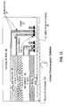
In general the photodetectors (sensors) of this and other embodiments can operate with a fixed bias voltage and output a current to the CMOS circuitry 16.
In the illustrated (non-limiting) embodiment an N-type Ge layer 20 is grown on the starting Ge (buffer) layer 14 to have a thickness of about 200 nm. The N-type Ge layer 20 can be doped with, for example, Arsenic with a dopant concentration of about 5E18 cm−3. A substantially undoped intrinsic Ge layer 22 is then grown to have a thickness of about 1000 nm, followed by the growth of a P-type Ge layer 24 having a thickness of about 200 nm. The P-type Ge layer 24 can be doped with, for example, Boron with a dopant concentration of about 5E18 cm−3. The layers 20, 22 and 24 will function in the final structure as the visible P-I-N photodetector.
Next a sequence of layers of Group III-V material is grown to form the IR photodetector. A first step in this process grows a substantially undoped InP/GaAs buffer layer 26 on the P-type Ge layer 24. A thickness of the InP/GaAs buffer layer 26 can be about 1 micron. This is followed by the growth of an N-type InGaAs layer 28 having, in a non-limiting embodiment, the composition In0.82Ga0.18As. The layer 28 can have a thickness of about 200 nm and is doped N-type using, for example, Si with a dopant concentration of about 5E18 cm−3. This is followed by the growth of a substantially undoped (intrinsic) layer of InGaAs layer 30 having, in a non-limiting embodiment, the composition In0.82Ga0.18As. The layer 30 can have a thickness of about 1000 nm. This is followed by the growth of a P-type InGaAs layer 32 having, in a non-limiting embodiment, the composition In0.82Ga0.18As. The layer 32 can have a thickness of about 200 nm and is doped P-type using, for example, Zn with a dopant concentration of about 5E18 cm−3. The layers 28, 30 and 32 will function in the final structure as the IR P-I-N photodetector.
In operation the incident EM radiation passes through the Si substrate 10A and the substantially transparent (at the wavelengths of interest) BOX layer 12. The shorter visible wavelengths are substantially absorbed in the Ge P-I-N photodetector to generate first photocarriers, while the longer wavelength IR radiation passes through the layers that comprise the Ge P-I-N photodetector is substantially absorbed in the InGaAs P-I-N photodetector to generate second photocarriers. These generated photocarriers are transported to the CMOS readout circuitry 16 via the metal interconnect layer 36 and the vertical interconnects 34.
InAlAs layer having, in a non-limiting embodiment, the composition In0.52Al0.48As and a thickness of about 200 nm. This layer can be doped P-type using, for example, Zn with a dopant concentration of about 5E18 cm−3.
In the photodetectors 54 and 56 the presence of the intrinsic layer is optional.
After forming the photodetectors 50-56 a mesa etch process is performed to expose edge surfaces (as in FIG. 4 ) and contacts are formed on the exposed edge surfaces. In this embodiment each photodetector 50-56 includes two edge contacts, one on the N-type material and one on the P-type material. Apertures are then opened, the CMOS readout circuit transistors have the contact silicide 16A formed (at a temperature of about 400° C.), followed by the formation of vertical conductive interconnects 34 (e.g., Cu, Al, Au, etc.) to the silicided contacts 16A and to the contacts formed on the edge portions of the photodetectors 50, 52, 54 and 56. Top-side horizontal metal traces are then added to connect the vertical conductive interconnects 34 of the photodetectors 50-54 to the vertical conductive interconnects 34 connected to the CMOS readout circuitry 16. In this front-side illuminated embodiment the top surface acts as a receiving surface for incident EM radiation.
It is pointed out that in this and the other described embodiments other photodetector types can be employed in addition to or in place of the photodetectors 50-56. For example, FIG. 6E shows an example of a quantum dot IR photodetector structure wherein a region containing InAs quantum dots is interposed between an N-type GaAs layer and a P-type GaAs layer, each having a thickness of, for example, about 200 nm. FIG. 6F shows an example of a Type II heterojunction IR photodetector structure, wherein thin layers of InAs and GaSb alternate with one another within a heterojunction region that is interposed between an N-type GaSb layer and a P-type GaSb layer, .each having a thickness of, for example, about 200 nm.
It is pointed out that in some of the photodetector embodiments described above the intrinsic layer can be omitted and replaced with a lightly doped layer.
The vertically stacked and lateral radiation detecting structures shown in FIGS. 4, 5, 9 and 10 each function as a single pixel in a multi-pixel radiation detector. In practice some thousands or millions of the stacked or lateral Ge P-I-N visible wavelength photodetectors and the stacked or lateral InGaAs P-I-N IR wavelength photodetectors (pixel structures) are fabricated on the common Si substrate 10 to form a FPA circuit. Additional circuitry, in addition to the CMOS readout circuitry 16, can also be provided such as conventional pixel row and column multiplexers, etc. All of this circuitry shares the common Si substrate in a monolithic manner. The same applies to the photoconductive embodiments such as the one shown in FIG. 12 . In embodiments of this invention there can be two, three, four or more discrete photodetectors provided per pixel, where each photodetector is responsive to a different range of EM radiation wavelengths (possibly overlapping a wavelength range or ranges of one or more other photodetectors within the pixel).
An integrated circuit in accordance with the present invention can be employed in applications, hardware, and/or electronic systems. Suitable hardware and systems in which such integrated circuits can be incorporated include, but are not limited to, any device wherein imaging capability is desired, including for example personal computers, portable computing and/or communications devices (e.g., cell phones) and stand-alone cameras and other imaging devices. Systems and hardware incorporating such integrated circuits are considered part of this invention. Given the teachings of the invention provided herein, one of ordinary skill in the art will be able to contemplate other implementations and applications of the techniques of the invention.
The terminology used herein is for the purpose of describing particular embodiments only and is not intended to be limiting of the invention. As used herein, the singular forms “a”, “an” and “the” are intended to include the plural forms as well, unless the context clearly indicates otherwise. It will be further understood that the terms “comprises” and/or “comprising,” when used in this specification, specify the presence of stated features, integers, steps, operations, elements, and/or components, but do not preclude the presence or addition of one or more other features, integers, steps, operations, elements, components, and/or groups thereof.
The corresponding structures, materials, acts, and equivalents of all means or step plus function elements in the claims below are intended to include any structure, material, or act for performing the function in combination with other claimed elements as specifically claimed. The description of the present invention has been presented for purposes of illustration and description, but is not intended to be exhaustive or limited to the invention in the form disclosed. Many modifications and variations will be apparent to those of ordinary skill in the art without departing from the scope and spirit of the invention. The embodiment was chosen and described in order to best explain the principles of the invention and the practical application, and to enable others of ordinary skill in the art to understand the invention for various embodiments with various modifications as are suited to the particular use contemplated.
As such, various modifications and adaptations may become apparent to those skilled in the relevant arts in view of the foregoing description, when read in conjunction with the accompanying drawings and the appended claims. As but some examples, the use of other similar or equivalent semiconductor fabrication processes, including deposition processes and etching processes may be used by those skilled in the art. Further, the exemplary embodiments are not intended to be limited to only those materials, metals, insulators, N-type dopants, P-type dopants, dopant concentrations, layer thicknesses and the like that were specifically disclosed above.
For example, the embodiments of this invention can be practiced using Group II-VI materials.
Furthermore, the invention is not to be construed as being limited to only the specific Group III-V compositions described above. For example, other relative percentages of the constituent Group III-V materials can be used and thus the wavelength absorption range adjusted accordingly.
Any and all such and similar modifications of the teachings of this invention will still fall within the scope of this invention.
Claims (16)
1. A method, comprising
providing a silicon substrate;
forming silicon readout circuitry on a first portion of a top surface of the silicon substrate; and
forming a radiation detecting pixel on a second portion of the top surface of the silicon substrate, the radiation detecting pixel being comprised of a plurality of radiation detectors connected with the silicon readout circuitry, where the plurality of radiation detectors are formed to comprise at least one visible wavelength radiation detector comprised of germanium and at least one infrared wavelength radiation detector comprised of a Group III-V semiconductor material;
where the at least one visible wavelength radiation detector comprised of germanium is formed to comprise a first P-I-N photodetector, where the at least one infrared wavelength radiation detector comprised of Group III-V semiconductor material is formed to comprise a second P-I-N photodetector that is disposed vertically above the visible wavelength radiation detector comprised of germanium, and further comprising forming a buffer layer comprised ofGroup III-V material that is interposed between, the first P-I-N photodetector and the second PI-N photodetector, further comprising thinning the silicon substrate, where a bottom surface of the thinned silicon substrate opposite the top surface of the silicon substrate is a radiation receiving surface.
2. The method as in claim 1 , where the substrate comprises a layer of oxide disposed on the second portion of the surface of the silicon substrate and a layer of germanium disposed on the layer of oxide, where the plurality of radiation detectors are formed to each comprise a plurality of layers of semiconductor material disposed above the layer of germanium and vertically adjacent to one another in a stacked manner.
3. The method as in claim 1 , where the substrate comprises a layer of oxide disposed on the second portion of the surface of the silicon substrate and a layer of germanium disposed on the layer of oxide, where the plurality of radiation detectors are formed to each comprise a plurality of layers of semiconductor material disposed above the layer of germanium and laterally adjacent to one another.
4. The method as in claim 1 , where the substrate comprises a layer of germanium disposed on the second portion of the surface of the silicon substrate, where the plurality of radiation detectors are formed to each comprise a plurality of layers of semiconductor material disposed above the layer of germanium and vertically adjacent to one another in a stacked manner.
5. The method as in claim 1 , where the substrate comprises a layer of germanium disposed on the second portion of the surface of the silicon substrate, where the plurality of radiation detectors are formed to each comprise a plurality of layers of semiconductor material disposed above the layer of germanium and laterally adjacent to one another.
6. The method as in claim 1 , where the at least one visible wavelength radiation detector comprised of germanium is formed to comprise a P-I-N photodetector and where the at least one infrared wavelength radiation detector comprised of Group III-V semiconductor material is formed to comprise a P-I-N photodetector.
7. The method as in claim 1 , where the at least one visible wavelength radiation detector comprised of germanium is formed to comprise a photoconductive layer and where the at least one infrared wavelength radiation detector comprised of Group III-V semiconductor material is formed to comprise a photoconductive layer.
8. The method as in claim 1 , further comprising recessing the second portion of the surface of the silicon substrate so as to be below the first portion of the surface of the silicon substrate prior to forming the radiation detecting pixel.
9. A method, comprising
providing a silicon substrate;
forming silicon readout circuitry on a first portion of a top surface of the silicon substrate; and
forming a radiation detecting pixel on a second portion of the top surface of the silicon substrate, the radiation detecting pixel being comprised of a plurality of radiation detectors connected with the silicon readout circuitry, where the plurality of radiation detectors are formed to comprise at least one visible wavelength radiation detector comprised of germanium and at least one infrared wavelength radiation detector comprised of a Group III-V semiconductor material;
where the substrate comprises a layer of germanium disposed on the second portion of the surface of the silicon substrate, where the at least one visible wavelength radiation detector comprised of germanium is formed to comprise a first P-I-N photodetector disposed on the layer of germanium, where the at least one infrared wavelength radiation detector comprised of Group III-V semiconductor material is formed to comprise a second P-I-N photodetector that is disposed above the layer of germanium and laterally adjacent to the visible wavelength radiation, detector comprised of germanium, and further comprising forming a buffer layer comprised of Group III-V material that is interposed between the second P-I-N photodetector and the layer of germanium, and where a radiation receiving surface of the structure is a surface opposite to a bottom surface of the silicon substrate.
10. The method as in claim 9 , where the substrate comprises a layer of oxide disposed on the second portion of the surface of the silicon substrate and a layer of germanium disposed on the layer of oxide, where the plurality of radiation detectors are formed to each comprise a plurality of layers of semiconductor material disposed above the layer of germanium and vertically adjacent to one another in a stacked manner.
11. The method as in claim 9 , where the substrate comprises a layer of oxide disposed on the second portion of the surface of the silicon substrate and a layer of germanium disposed on the layer of oxide, where the plurality of radiation detectors are formed to each comprise a plurality of layers of semiconductor material disposed above the layer of germanium and laterally adjacent to one another.
12. The method as in claim 9 , where the substrate comprises a layer of germanium disposed on the second portion of the surface of the silicon substrate, where the plurality of radiation detectors are formed to each comprise a plurality of layers of semiconductor material disposed above the layer of germanium and vertically adjacent to one another in a stacked manner.
13. The method as in claim 9 , where the substrate comprises a layer of germanium disposed on the second portion of the surface of the silicon substrate, where the plurality of radiation detectors are formed to each comprise a plurality of layers of semiconductor material disposed above the layer of germanium and laterally adjacent to one another.
14. The method as in claim 9 , where the at least one visible wavelength radiation detector comprised of germanium is formed to comprise a P-I-N photodetector and where the at least one infrared wavelength radiation detector comprised of Group III-V semiconductor material is formed to comprise a P-I-N photodetector.
15. The method as in claim 9 , where the at least one visible wavelength radiation detector comprised of germanium is formed to comprise a photoconductive layer and where the at least one infrared wavelength radiation detector comprised of Group III-V semiconductor material is formed to comprise a photoconductive layer.
16. The method as in claim 9 , further comprising recessing the second portion of the surface of the silicon substrate so as to be below the first portion of the surface of the silicon substrate prior to forming the radiation detecting pixel.
Priority Applications (1)
| Application Number | Priority Date | Filing Date | Title |
|---|---|---|---|
| US15/415,281 US9911784B2 (en) | 2015-06-19 | 2017-01-25 | Monolithic visible-infrared focal plane array on silicon |
Applications Claiming Priority (3)
| Application Number | Priority Date | Filing Date | Title |
|---|---|---|---|
| US14/744,210 US9472588B1 (en) | 2015-06-19 | 2015-06-19 | Monolithic visible-infrared focal plane array on silicon |
| US15/196,307 US9685481B2 (en) | 2015-06-19 | 2016-06-29 | Monolithic visible-infrared focal plane array on silicon |
| US15/415,281 US9911784B2 (en) | 2015-06-19 | 2017-01-25 | Monolithic visible-infrared focal plane array on silicon |
Related Parent Applications (1)
| Application Number | Title | Priority Date | Filing Date |
|---|---|---|---|
| US15/196,307 Continuation US9685481B2 (en) | 2015-06-19 | 2016-06-29 | Monolithic visible-infrared focal plane array on silicon |
Publications (2)
| Publication Number | Publication Date |
|---|---|
| US20170133416A1 US20170133416A1 (en) | 2017-05-11 |
| US9911784B2 true US9911784B2 (en) | 2018-03-06 |
Family
ID=57120278
Family Applications (5)
| Application Number | Title | Priority Date | Filing Date |
|---|---|---|---|
| US14/744,210 Active US9472588B1 (en) | 2015-06-19 | 2015-06-19 | Monolithic visible-infrared focal plane array on silicon |
| US15/196,378 Active US9917122B2 (en) | 2015-06-19 | 2016-06-29 | Monolithic visible-infrared focal plane array on silicon |
| US15/196,307 Expired - Fee Related US9685481B2 (en) | 2015-06-19 | 2016-06-29 | Monolithic visible-infrared focal plane array on silicon |
| US15/415,281 Active US9911784B2 (en) | 2015-06-19 | 2017-01-25 | Monolithic visible-infrared focal plane array on silicon |
| US15/416,301 Active US10043845B2 (en) | 2015-06-19 | 2017-01-26 | Monolithic visible-infrared focal plane array on silicon |
Family Applications Before (3)
| Application Number | Title | Priority Date | Filing Date |
|---|---|---|---|
| US14/744,210 Active US9472588B1 (en) | 2015-06-19 | 2015-06-19 | Monolithic visible-infrared focal plane array on silicon |
| US15/196,378 Active US9917122B2 (en) | 2015-06-19 | 2016-06-29 | Monolithic visible-infrared focal plane array on silicon |
| US15/196,307 Expired - Fee Related US9685481B2 (en) | 2015-06-19 | 2016-06-29 | Monolithic visible-infrared focal plane array on silicon |
Family Applications After (1)
| Application Number | Title | Priority Date | Filing Date |
|---|---|---|---|
| US15/416,301 Active US10043845B2 (en) | 2015-06-19 | 2017-01-26 | Monolithic visible-infrared focal plane array on silicon |
Country Status (1)
| Country | Link |
|---|---|
| US (5) | US9472588B1 (en) |
Families Citing this family (28)
| Publication number | Priority date | Publication date | Assignee | Title |
|---|---|---|---|---|
| US9472588B1 (en) | 2015-06-19 | 2016-10-18 | International Business Machines Corporation | Monolithic visible-infrared focal plane array on silicon |
| JP2017022175A (en) * | 2015-07-07 | 2017-01-26 | ルネサスエレクトロニクス株式会社 | Semiconductor device and manufacturing method of the same |
| CN108352393B (en) | 2015-07-23 | 2022-09-16 | 光程研创股份有限公司 | High-efficiency wide-spectrum sensor |
| US10644187B2 (en) | 2015-07-24 | 2020-05-05 | Artilux, Inc. | Multi-wafer based light absorption apparatus and applications thereof |
| TWI713556B (en) * | 2015-07-24 | 2020-12-21 | 光澄科技股份有限公司 | Semiconductor light absorption structure and light absorption apparatus |
| EP3709362B1 (en) | 2015-08-04 | 2021-07-14 | Artilux Inc. | Germanium-silicon light sensing method |
| US10707260B2 (en) | 2015-08-04 | 2020-07-07 | Artilux, Inc. | Circuit for operating a multi-gate VIS/IR photodiode |
| US10761599B2 (en) | 2015-08-04 | 2020-09-01 | Artilux, Inc. | Eye gesture tracking |
| US10861888B2 (en) | 2015-08-04 | 2020-12-08 | Artilux, Inc. | Silicon germanium imager with photodiode in trench |
| CN115824395B (en) * | 2015-08-27 | 2023-08-15 | 光程研创股份有限公司 | Wide-spectrum optical sensor |
| US10741598B2 (en) | 2015-11-06 | 2020-08-11 | Atrilux, Inc. | High-speed light sensing apparatus II |
| US10739443B2 (en) | 2015-11-06 | 2020-08-11 | Artilux, Inc. | High-speed light sensing apparatus II |
| US10886309B2 (en) | 2015-11-06 | 2021-01-05 | Artilux, Inc. | High-speed light sensing apparatus II |
| US10418407B2 (en) | 2015-11-06 | 2019-09-17 | Artilux, Inc. | High-speed light sensing apparatus III |
| US10254389B2 (en) | 2015-11-06 | 2019-04-09 | Artilux Corporation | High-speed light sensing apparatus |
| US10823607B2 (en) * | 2016-12-08 | 2020-11-03 | The United States Of America, As Represented By The Secretary Of The Navy | Systems and methods for converting, delaying, and measuring electromagnetic energy or wave(s) input within a first frequency range to one or more frequencies within a second frequency range with predetermined time delay(s) for use in applications including data collection, imaging or astronomy |
| US11007721B2 (en) | 2017-06-02 | 2021-05-18 | 3D Systems, Inc. | Three dimensional printing system with improved reliability, safety, and quality |
| JP6975341B2 (en) | 2018-02-23 | 2021-12-01 | アーティラックス・インコーポレイテッド | Photodetector and its light detection method |
| US11482553B2 (en) | 2018-02-23 | 2022-10-25 | Artilux, Inc. | Photo-detecting apparatus with subpixels |
| US11105928B2 (en) | 2018-02-23 | 2021-08-31 | Artilux, Inc. | Light-sensing apparatus and light-sensing method thereof |
| JP7212062B2 (en) * | 2018-04-08 | 2023-01-24 | アーティラックス・インコーポレイテッド | Photodetector |
| US10854770B2 (en) | 2018-05-07 | 2020-12-01 | Artilux, Inc. | Avalanche photo-transistor |
| US10969877B2 (en) | 2018-05-08 | 2021-04-06 | Artilux, Inc. | Display apparatus |
| WO2019219189A1 (en) * | 2018-05-16 | 2019-11-21 | Iris Industries Sa | Short-wave infrared detector and its integration with cmos compatible substrates |
| CN110277053B (en) * | 2019-06-25 | 2020-12-08 | 京东方科技集团股份有限公司 | Display panel, manufacturing method and driving method thereof, and display device |
| US11652184B2 (en) | 2019-08-28 | 2023-05-16 | Artilux, Inc. | Photo-detecting apparatus with low dark current |
| US11837613B2 (en) * | 2020-05-29 | 2023-12-05 | Taiwan Semiconductor Manufacturing Company Limited | Germanium-containing photodetector and methods of forming the same |
| CN113363342B (en) * | 2021-06-04 | 2022-10-28 | 中国科学技术大学 | Ga-GaSb silicon-based near-infrared photoelectric detector and preparation method thereof |
Citations (13)
| Publication number | Priority date | Publication date | Assignee | Title |
|---|---|---|---|---|
| US5479032A (en) | 1994-07-21 | 1995-12-26 | Trustees Of Princeton University | Multiwavelength infrared focal plane array detector |
| US5518934A (en) | 1994-07-21 | 1996-05-21 | Trustees Of Princeton University | Method of fabricating multiwavelength infrared focal plane array detector |
| US5981950A (en) | 1997-02-07 | 1999-11-09 | Commissariat A L'energie Atomique | Multicolor photonic radiation detector |
| US6107618A (en) | 1997-07-14 | 2000-08-22 | California Institute Of Technology | Integrated infrared and visible image sensors |
| US6407439B1 (en) | 1999-08-19 | 2002-06-18 | Epitaxial Technologies, Llc | Programmable multi-wavelength detector array |
| US7592593B2 (en) | 2006-07-26 | 2009-09-22 | Northrop Grumman Corporation | Multi-band focal plane array |
| US7838869B2 (en) | 2005-10-21 | 2010-11-23 | Georgia State University Research Foundation, Inc. | Dual band photodetector |
| US7972885B1 (en) | 2008-09-25 | 2011-07-05 | Banpil Photonics, Inc. | Broadband imaging device and manufacturing thereof |
| US8299485B2 (en) | 2008-03-19 | 2012-10-30 | Soitec | Substrates for monolithic optical circuits and electronic circuits |
| US20130193308A1 (en) | 2011-12-21 | 2013-08-01 | Arizona State | Multiband Photodetector Utilizing Unipolar and Bipolar Devices |
| DE102012214690A1 (en) | 2012-08-17 | 2014-02-20 | Fraunhofer-Gesellschaft zur Förderung der angewandten Forschung e.V. | Electromagnetic radiation detector for wide-band multi-spectral imaging device, has lower detection structure that is arranged within lower semiconductor chip to overlap with upper detection structure arranged within upper chip |
| US20140138543A1 (en) | 2011-10-21 | 2014-05-22 | Santa Barbara Infrared, Inc. | Techniques for Tiling Arrays of Pixel Elements |
| US9472588B1 (en) | 2015-06-19 | 2016-10-18 | International Business Machines Corporation | Monolithic visible-infrared focal plane array on silicon |
-
2015
- 2015-06-19 US US14/744,210 patent/US9472588B1/en active Active
-
2016
- 2016-06-29 US US15/196,378 patent/US9917122B2/en active Active
- 2016-06-29 US US15/196,307 patent/US9685481B2/en not_active Expired - Fee Related
-
2017
- 2017-01-25 US US15/415,281 patent/US9911784B2/en active Active
- 2017-01-26 US US15/416,301 patent/US10043845B2/en active Active
Patent Citations (15)
| Publication number | Priority date | Publication date | Assignee | Title |
|---|---|---|---|---|
| US5479032A (en) | 1994-07-21 | 1995-12-26 | Trustees Of Princeton University | Multiwavelength infrared focal plane array detector |
| US5518934A (en) | 1994-07-21 | 1996-05-21 | Trustees Of Princeton University | Method of fabricating multiwavelength infrared focal plane array detector |
| US5981950A (en) | 1997-02-07 | 1999-11-09 | Commissariat A L'energie Atomique | Multicolor photonic radiation detector |
| US6107618A (en) | 1997-07-14 | 2000-08-22 | California Institute Of Technology | Integrated infrared and visible image sensors |
| US6407439B1 (en) | 1999-08-19 | 2002-06-18 | Epitaxial Technologies, Llc | Programmable multi-wavelength detector array |
| US7838869B2 (en) | 2005-10-21 | 2010-11-23 | Georgia State University Research Foundation, Inc. | Dual band photodetector |
| US7592593B2 (en) | 2006-07-26 | 2009-09-22 | Northrop Grumman Corporation | Multi-band focal plane array |
| US8299485B2 (en) | 2008-03-19 | 2012-10-30 | Soitec | Substrates for monolithic optical circuits and electronic circuits |
| US7972885B1 (en) | 2008-09-25 | 2011-07-05 | Banpil Photonics, Inc. | Broadband imaging device and manufacturing thereof |
| US8035184B1 (en) | 2008-09-25 | 2011-10-11 | Banpil Photonics, Inc. | Broadband imaging device |
| US20140138543A1 (en) | 2011-10-21 | 2014-05-22 | Santa Barbara Infrared, Inc. | Techniques for Tiling Arrays of Pixel Elements |
| US20130193308A1 (en) | 2011-12-21 | 2013-08-01 | Arizona State | Multiband Photodetector Utilizing Unipolar and Bipolar Devices |
| DE102012214690A1 (en) | 2012-08-17 | 2014-02-20 | Fraunhofer-Gesellschaft zur Förderung der angewandten Forschung e.V. | Electromagnetic radiation detector for wide-band multi-spectral imaging device, has lower detection structure that is arranged within lower semiconductor chip to overlap with upper detection structure arranged within upper chip |
| US9472588B1 (en) | 2015-06-19 | 2016-10-18 | International Business Machines Corporation | Monolithic visible-infrared focal plane array on silicon |
| US9685481B2 (en) | 2015-06-19 | 2017-06-20 | International Business Machines Corporation | Monolithic visible-infrared focal plane array on silicon |
Non-Patent Citations (2)
| Title |
|---|
| List of IBM Patents or Applications Treated as Related, 2 pgs. |
| Machine Translation of DE 10 2012 214 690 A1. |
Also Published As
| Publication number | Publication date |
|---|---|
| US9472588B1 (en) | 2016-10-18 |
| US9917122B2 (en) | 2018-03-13 |
| US9685481B2 (en) | 2017-06-20 |
| US20170133427A1 (en) | 2017-05-11 |
| US20170229507A1 (en) | 2017-08-10 |
| US20160372502A1 (en) | 2016-12-22 |
| US20170133416A1 (en) | 2017-05-11 |
| US10043845B2 (en) | 2018-08-07 |
Similar Documents
| Publication | Publication Date | Title |
|---|---|---|
| US9911784B2 (en) | Monolithic visible-infrared focal plane array on silicon | |
| US9105549B2 (en) | Semiconductor sensor structures with reduced dislocation defect densities | |
| US7906825B2 (en) | Ge imager for short wavelength infrared | |
| US10854656B2 (en) | Short-wave infrared detector array and method for the manufacturing thereof | |
| JP6400031B2 (en) | Circuit structure, sensor structure and structure | |
| US8022390B1 (en) | Lateral conduction infrared photodetector | |
| US5808329A (en) | Low light level imager with extended wavelength response employing atomic bonded (fused) semiconductor materials | |
| Rogalski | HgCdTe photodetectors | |
| US20220093812A1 (en) | Passivated photodiode comprising a ferroelectric peripheral portion | |
| KR20140030265A (en) | Passivated upstanding nanostructures and methods of making the same | |
| US20190371947A1 (en) | Optoelectronic devices formed over a buffer | |
| US11851785B2 (en) | Aluminum nitride passivation layer for mercury cadmium telluride in an electrical device | |
| US11894480B2 (en) | Low leakage current germanium-on-silicon photo-devices | |
| US11227968B2 (en) | Method for improved manufacturing of a photodiode-based optical sensor and associated device | |
| US9209216B2 (en) | Passivation of back-illuminated image sensor | |
| CN115377135A (en) | Infrared detector, imaging chip and preparation method thereof |
Legal Events
| Date | Code | Title | Description |
|---|---|---|---|
| AS | Assignment |
Owner name: INTERNATIONAL BUSINESS MACHINES CORPORATION, NEW Y Free format text: ASSIGNMENT OF ASSIGNORS INTEREST;ASSIGNORS:LI, NING;SADANA, DEVENDRA K.;WISNIEFF, ROBERT L.;SIGNING DATES FROM 20150730 TO 20150814;REEL/FRAME:041081/0407 |
|
| STCF | Information on status: patent grant |
Free format text: PATENTED CASE |
|
| MAFP | Maintenance fee payment |
Free format text: PAYMENT OF MAINTENANCE FEE, 4TH YEAR, LARGE ENTITY (ORIGINAL EVENT CODE: M1551); ENTITY STATUS OF PATENT OWNER: LARGE ENTITY Year of fee payment: 4 |