US9906221B1 - Driving circuit of a power circuit - Google Patents
Driving circuit of a power circuit Download PDFInfo
- Publication number
- US9906221B1 US9906221B1 US15/395,738 US201615395738A US9906221B1 US 9906221 B1 US9906221 B1 US 9906221B1 US 201615395738 A US201615395738 A US 201615395738A US 9906221 B1 US9906221 B1 US 9906221B1
- Authority
- US
- United States
- Prior art keywords
- node
- transistor
- driving
- normally
- voltage
- Prior art date
- Legal status (The legal status is an assumption and is not a legal conclusion. Google has not performed a legal analysis and makes no representation as to the accuracy of the status listed.)
- Active
Links
- 230000008878 coupling Effects 0.000 claims abstract 5
- 238000010168 coupling process Methods 0.000 claims abstract 5
- 238000005859 coupling reaction Methods 0.000 claims abstract 5
- 239000003990 capacitor Substances 0.000 claims description 23
- 238000010586 diagram Methods 0.000 description 12
- 230000003071 parasitic effect Effects 0.000 description 4
- 230000004075 alteration Effects 0.000 description 1
- 230000015572 biosynthetic process Effects 0.000 description 1
- 230000004048 modification Effects 0.000 description 1
- 238000012986 modification Methods 0.000 description 1
- ZMRUPTIKESYGQW-UHFFFAOYSA-N propranolol hydrochloride Chemical compound [H+].[Cl-].C1=CC=C2C(OCC(O)CNC(C)C)=CC=CC2=C1 ZMRUPTIKESYGQW-UHFFFAOYSA-N 0.000 description 1
- 230000000630 rising effect Effects 0.000 description 1
Images


Classifications
-
- H—ELECTRICITY
- H02—GENERATION; CONVERSION OR DISTRIBUTION OF ELECTRIC POWER
- H02M—APPARATUS FOR CONVERSION BETWEEN AC AND AC, BETWEEN AC AND DC, OR BETWEEN DC AND DC, AND FOR USE WITH MAINS OR SIMILAR POWER SUPPLY SYSTEMS; CONVERSION OF DC OR AC INPUT POWER INTO SURGE OUTPUT POWER; CONTROL OR REGULATION THEREOF
- H02M1/00—Details of apparatus for conversion
- H02M1/08—Circuits specially adapted for the generation of control voltages for semiconductor devices incorporated in static converters
- H02M1/088—Circuits specially adapted for the generation of control voltages for semiconductor devices incorporated in static converters for the simultaneous control of series or parallel connected semiconductor devices
-
- H—ELECTRICITY
- H03—ELECTRONIC CIRCUITRY
- H03K—PULSE TECHNIQUE
- H03K17/00—Electronic switching or gating, i.e. not by contact-making and –breaking
- H03K17/16—Modifications for eliminating interference voltages or currents
- H03K17/161—Modifications for eliminating interference voltages or currents in field-effect transistor switches
-
- H—ELECTRICITY
- H03—ELECTRONIC CIRCUITRY
- H03K—PULSE TECHNIQUE
- H03K3/00—Circuits for generating electric pulses; Monostable, bistable or multistable circuits
- H03K3/02—Generators characterised by the type of circuit or by the means used for producing pulses
- H03K3/353—Generators characterised by the type of circuit or by the means used for producing pulses by the use, as active elements, of field-effect transistors with internal or external positive feedback
- H03K3/356—Bistable circuits
- H03K3/3565—Bistables with hysteresis, e.g. Schmitt trigger
-
- H—ELECTRICITY
- H01—ELECTRIC ELEMENTS
- H01L—SEMICONDUCTOR DEVICES NOT COVERED BY CLASS H10
- H01L29/00—Semiconductor devices specially adapted for rectifying, amplifying, oscillating or switching and having potential barriers; Capacitors or resistors having potential barriers, e.g. a PN-junction depletion layer or carrier concentration layer; Details of semiconductor bodies or of electrodes thereof ; Multistep manufacturing processes therefor
- H01L29/02—Semiconductor bodies ; Multistep manufacturing processes therefor
- H01L29/12—Semiconductor bodies ; Multistep manufacturing processes therefor characterised by the materials of which they are formed
- H01L29/20—Semiconductor bodies ; Multistep manufacturing processes therefor characterised by the materials of which they are formed including, apart from doping materials or other impurities, only AIIIBV compounds
- H01L29/2003—Nitride compounds
-
- H—ELECTRICITY
- H02—GENERATION; CONVERSION OR DISTRIBUTION OF ELECTRIC POWER
- H02M—APPARATUS FOR CONVERSION BETWEEN AC AND AC, BETWEEN AC AND DC, OR BETWEEN DC AND DC, AND FOR USE WITH MAINS OR SIMILAR POWER SUPPLY SYSTEMS; CONVERSION OF DC OR AC INPUT POWER INTO SURGE OUTPUT POWER; CONTROL OR REGULATION THEREOF
- H02M1/00—Details of apparatus for conversion
- H02M1/08—Circuits specially adapted for the generation of control voltages for semiconductor devices incorporated in static converters
-
- H—ELECTRICITY
- H02—GENERATION; CONVERSION OR DISTRIBUTION OF ELECTRIC POWER
- H02M—APPARATUS FOR CONVERSION BETWEEN AC AND AC, BETWEEN AC AND DC, OR BETWEEN DC AND DC, AND FOR USE WITH MAINS OR SIMILAR POWER SUPPLY SYSTEMS; CONVERSION OF DC OR AC INPUT POWER INTO SURGE OUTPUT POWER; CONTROL OR REGULATION THEREOF
- H02M1/00—Details of apparatus for conversion
- H02M1/44—Circuits or arrangements for compensating for electromagnetic interference in converters or inverters
-
- H—ELECTRICITY
- H02—GENERATION; CONVERSION OR DISTRIBUTION OF ELECTRIC POWER
- H02M—APPARATUS FOR CONVERSION BETWEEN AC AND AC, BETWEEN AC AND DC, OR BETWEEN DC AND DC, AND FOR USE WITH MAINS OR SIMILAR POWER SUPPLY SYSTEMS; CONVERSION OF DC OR AC INPUT POWER INTO SURGE OUTPUT POWER; CONTROL OR REGULATION THEREOF
- H02M3/00—Conversion of dc power input into dc power output
- H02M3/02—Conversion of dc power input into dc power output without intermediate conversion into ac
- H02M3/04—Conversion of dc power input into dc power output without intermediate conversion into ac by static converters
- H02M3/06—Conversion of dc power input into dc power output without intermediate conversion into ac by static converters using resistors or capacitors, e.g. potential divider
- H02M3/07—Conversion of dc power input into dc power output without intermediate conversion into ac by static converters using resistors or capacitors, e.g. potential divider using capacitors charged and discharged alternately by semiconductor devices with control electrode, e.g. charge pumps
-
- H—ELECTRICITY
- H02—GENERATION; CONVERSION OR DISTRIBUTION OF ELECTRIC POWER
- H02M—APPARATUS FOR CONVERSION BETWEEN AC AND AC, BETWEEN AC AND DC, OR BETWEEN DC AND DC, AND FOR USE WITH MAINS OR SIMILAR POWER SUPPLY SYSTEMS; CONVERSION OF DC OR AC INPUT POWER INTO SURGE OUTPUT POWER; CONTROL OR REGULATION THEREOF
- H02M3/00—Conversion of dc power input into dc power output
- H02M3/02—Conversion of dc power input into dc power output without intermediate conversion into ac
- H02M3/04—Conversion of dc power input into dc power output without intermediate conversion into ac by static converters
- H02M3/10—Conversion of dc power input into dc power output without intermediate conversion into ac by static converters using discharge tubes with control electrode or semiconductor devices with control electrode
- H02M3/145—Conversion of dc power input into dc power output without intermediate conversion into ac by static converters using discharge tubes with control electrode or semiconductor devices with control electrode using devices of a triode or transistor type requiring continuous application of a control signal
- H02M3/155—Conversion of dc power input into dc power output without intermediate conversion into ac by static converters using discharge tubes with control electrode or semiconductor devices with control electrode using devices of a triode or transistor type requiring continuous application of a control signal using semiconductor devices only
- H02M3/156—Conversion of dc power input into dc power output without intermediate conversion into ac by static converters using discharge tubes with control electrode or semiconductor devices with control electrode using devices of a triode or transistor type requiring continuous application of a control signal using semiconductor devices only with automatic control of output voltage or current, e.g. switching regulators
- H02M3/158—Conversion of dc power input into dc power output without intermediate conversion into ac by static converters using discharge tubes with control electrode or semiconductor devices with control electrode using devices of a triode or transistor type requiring continuous application of a control signal using semiconductor devices only with automatic control of output voltage or current, e.g. switching regulators including plural semiconductor devices as final control devices for a single load
- H02M3/1588—Conversion of dc power input into dc power output without intermediate conversion into ac by static converters using discharge tubes with control electrode or semiconductor devices with control electrode using devices of a triode or transistor type requiring continuous application of a control signal using semiconductor devices only with automatic control of output voltage or current, e.g. switching regulators including plural semiconductor devices as final control devices for a single load comprising at least one synchronous rectifier element
-
- H—ELECTRICITY
- H03—ELECTRONIC CIRCUITRY
- H03F—AMPLIFIERS
- H03F3/00—Amplifiers with only discharge tubes or only semiconductor devices as amplifying elements
- H03F3/45—Differential amplifiers
- H03F3/45071—Differential amplifiers with semiconductor devices only
- H03F3/45076—Differential amplifiers with semiconductor devices only characterised by the way of implementation of the active amplifying circuit in the differential amplifier
- H03F3/45475—Differential amplifiers with semiconductor devices only characterised by the way of implementation of the active amplifying circuit in the differential amplifier using IC blocks as the active amplifying circuit
-
- H—ELECTRICITY
- H03—ELECTRONIC CIRCUITRY
- H03K—PULSE TECHNIQUE
- H03K17/00—Electronic switching or gating, i.e. not by contact-making and –breaking
- H03K17/06—Modifications for ensuring a fully conducting state
- H03K17/063—Modifications for ensuring a fully conducting state in field-effect transistor switches
-
- H—ELECTRICITY
- H03—ELECTRONIC CIRCUITRY
- H03K—PULSE TECHNIQUE
- H03K17/00—Electronic switching or gating, i.e. not by contact-making and –breaking
- H03K17/51—Electronic switching or gating, i.e. not by contact-making and –breaking characterised by the components used
- H03K17/56—Electronic switching or gating, i.e. not by contact-making and –breaking characterised by the components used by the use, as active elements, of semiconductor devices
- H03K17/687—Electronic switching or gating, i.e. not by contact-making and –breaking characterised by the components used by the use, as active elements, of semiconductor devices the devices being field-effect transistors
- H03K17/6871—Electronic switching or gating, i.e. not by contact-making and –breaking characterised by the components used by the use, as active elements, of semiconductor devices the devices being field-effect transistors the output circuit comprising more than one controlled field-effect transistor
-
- H—ELECTRICITY
- H02—GENERATION; CONVERSION OR DISTRIBUTION OF ELECTRIC POWER
- H02M—APPARATUS FOR CONVERSION BETWEEN AC AND AC, BETWEEN AC AND DC, OR BETWEEN DC AND DC, AND FOR USE WITH MAINS OR SIMILAR POWER SUPPLY SYSTEMS; CONVERSION OF DC OR AC INPUT POWER INTO SURGE OUTPUT POWER; CONTROL OR REGULATION THEREOF
- H02M1/00—Details of apparatus for conversion
- H02M1/0003—Details of control, feedback or regulation circuits
- H02M1/0006—Arrangements for supplying an adequate voltage to the control circuit of converters
-
- H—ELECTRICITY
- H03—ELECTRONIC CIRCUITRY
- H03F—AMPLIFIERS
- H03F3/00—Amplifiers with only discharge tubes or only semiconductor devices as amplifying elements
- H03F3/45—Differential amplifiers
-
- H—ELECTRICITY
- H03—ELECTRONIC CIRCUITRY
- H03K—PULSE TECHNIQUE
- H03K2217/00—Indexing scheme related to electronic switching or gating, i.e. not by contact-making or -breaking covered by H03K17/00
- H03K2217/0063—High side switches, i.e. the higher potential [DC] or life wire [AC] being directly connected to the switch and not via the load
-
- H—ELECTRICITY
- H03—ELECTRONIC CIRCUITRY
- H03K—PULSE TECHNIQUE
- H03K2217/00—Indexing scheme related to electronic switching or gating, i.e. not by contact-making or -breaking covered by H03K17/00
- H03K2217/0072—Low side switches, i.e. the lower potential [DC] or neutral wire [AC] being directly connected to the switch and not via the load
-
- H—ELECTRICITY
- H03—ELECTRONIC CIRCUITRY
- H03K—PULSE TECHNIQUE
- H03K2217/00—Indexing scheme related to electronic switching or gating, i.e. not by contact-making or -breaking covered by H03K17/00
- H03K2217/0081—Power supply means, e.g. to the switch driver
-
- Y—GENERAL TAGGING OF NEW TECHNOLOGICAL DEVELOPMENTS; GENERAL TAGGING OF CROSS-SECTIONAL TECHNOLOGIES SPANNING OVER SEVERAL SECTIONS OF THE IPC; TECHNICAL SUBJECTS COVERED BY FORMER USPC CROSS-REFERENCE ART COLLECTIONS [XRACs] AND DIGESTS
- Y02—TECHNOLOGIES OR APPLICATIONS FOR MITIGATION OR ADAPTATION AGAINST CLIMATE CHANGE
- Y02B—CLIMATE CHANGE MITIGATION TECHNOLOGIES RELATED TO BUILDINGS, e.g. HOUSING, HOUSE APPLIANCES OR RELATED END-USER APPLICATIONS
- Y02B70/00—Technologies for an efficient end-user side electric power management and consumption
- Y02B70/10—Technologies improving the efficiency by using switched-mode power supplies [SMPS], i.e. efficient power electronics conversion e.g. power factor correction or reduction of losses in power supplies or efficient standby modes
Definitions
- the disclosure generally relates to a driving circuit integrated with a GaN power device.
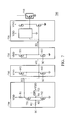
- FIG. 1 illustrates a conventional power circuit.
- the high-side driver DRV 1 is configured to drive the first power transistor 110 A
- the low-side driver DRV 2 is configured to drive the second power transistor 110 B.
- the boost capacitor CB and the boost diode DB are configured to boost the supply voltage VDD to the boost voltage VB, such that the first power transistor 110 A can be fully turned on. Therefore, the first power transistor 110 A supplied by the input voltage VIN and the second power transistor 110 B can drive the load device RL through the inductor L and the capacitor C.
- the inductor L may induce significant parasitic effects at the switch node SW (such as a negative voltage spike generated at the switch node SW by the turned-on body diode of the second power transistor 110 B), these parasitic effects can interfered with the boost voltage VB when the boost capacitor CB is charged through the power transistor. Therefore, it is necessary to eliminate parasitic effects from the driving circuit.
- the invention provides a driving circuit with a charge pump that is not charged through the power transistor to mitigate parasitic effects.
- a power circuit comprises a power transistor, a driving circuit, a first pre-driver, a second pre-driver, and a hysteresis circuit.
- the power transistor flows a power current to a ground according to a driving voltage of a driving node.
- the driving circuit comprises a high-side transistor, a low-side transistor, and a charge pump.
- the high-side transistor provides a supply voltage to the driving node according to a high-side voltage of a high-side node.
- the low-side transistor couples the driving node to the ground according to a first internal signal.
- the charge pump is coupled to the high-side node and the driving node, and is configured to generate the high-side voltage that exceeds the supply voltage according to the first internal signal.
- the first pre-driver receives a second internal signal to generate the first internal signal.
- the second pre-driver receives a third internal signal to generate the second internal signal.
- the hysteresis circuit receives a control signal to generate the third internal signal and is configured to provide a hysteresis for the control signal.
- the first pre-driver and the second pre-driver are configured to improve driving capability of the control signal.
- the high-side transistor and the low-side transistor are normally-off transistors.
- the power transistor is a GaN transistor.
- the charge pump comprises a first unidirectional conducting device, a capacitor, a discharge resistor, a second unidirectional conducting device, a third unidirectional conducting device, and a switch.
- the first unidirectional conducting device unidirectionally provides the supply voltage to a first node.
- the capacitor is coupled between the first node and a second node.
- the discharge resistor is coupled between the first node and the high-side node.
- the second unidirectional conducting device unidirectionally couples the second node to the high-side node when the voltage of the second node exceeds the voltage of the high-side node.
- the third unidirectional conducting device unidirectionally provides the driving voltage to the second node when the driving voltage exceeds the voltage of the second node.
- the switch receives the control signal and is configured to couple the high-side node to the ground according to the control signal.
- the switch when the control signal is at a high voltage level, the switch is turned ON and the capacitor is charged by the supply voltage through the first unidirectional conducting device, the second unidirectional conducting device, and the switch.
- the switch When the control signal is at a low voltage level, the switch is turned OFF, the third unidirectional conducting device provides the driving voltage to the second node, and the capacitor is discharged to the driving node through the discharge resistor.
- each of the first unidirectional conducting device, the second unidirectional conducting device, and the third unidirectional conducting device is a diode or a diode-connected normally-off transistor.
- the driving circuit further comprises a high-side normally-on transistor.
- the high-side normally-on transistor comprises a source terminal coupled to the driving node, a gate terminal coupled to the driving node, and a drain terminal supplied by the supply voltage.
- the high-side normally-on transistor is configured to improve the driving capability of the high-side transistor.
- the first pre-driver comprises a first normally-on transistor and a first normally-off transistor.
- the first normally-on transistor comprises a gate terminal coupled to the driving circuit, a source terminal coupled to the driving circuit, and a drain terminal supplied by the supply voltage.
- the first normally-off transistor comprises a gate terminal receiving the control signal, a source terminal coupled to the ground, and a drain terminal coupled to the driving circuit.
- the second pre-driver comprises a second normally-on transistor and a second normally-off transistor.
- the second normally-on transistor comprises a gate terminal coupled to the gate terminal of the first normally-off transistor, a source terminal coupled to the gate terminal of the first normally-off transistor, and a drain terminal supplied by the supply voltage.
- the second normally-off transistor comprises a gate tell sinal receiving the control signal, a source terminal coupled to the ground, and a drain terminal coupled to the gate terminal of the first normally-off transistor.
- the hysteresis circuit comprises a first resistor, a third normally-off transistor, a fourth normally-off transistor, a fifth normally-off transistor, and a second resistor.
- the first resistor is coupled to the supply voltage.
- the third normally-off transistor comprises a gate terminal coupled to a third node, a source terminal coupled to a fourth node, and a drain terminal coupled to the first resistor.
- the fourth normally-off transistor comprises a gate terminal coupled to the third node, a source terminal coupled to the ground, and a drain terminal coupled to the fourth node.
- the fifth normally-off transistor comprises a gate terminal coupled to the first resistor, a source terminal coupled to the fourth node, and a drain terminal supplied by the supply voltage.
- the second resistor is coupled to the third node and receives the control signal.
- a driving circuit for driving a power transistor which flows a power current to a ground according to a driving voltage of a driving node, comprises a high-side transistor, a low-side transistor, a charge pump, a first pre-driver, a second pre-driver, and a hysteresis circuit.
- the high-side transistor provides a supply voltage to the driving node according to a high-side voltage of a high-side node.
- the low-side transistor couples the driving node to the ground according to a first internal signal.
- the charge pump is coupled to the high-side node and the driving node, and is configured to generate the high-side voltage that exceeds the supply voltage according to the first internal signal.
- the first pre-driver receives a second internal signal to generate the first internal signal.
- the second pre-driver receives a third internal signal to generate the second internal signal.
- the hysteresis circuit receives a control signal to generate the third internal signal and is configured to provide a hysteresis function for the control signal.
- the first pre-driver and the second pre-driver are configured to improve driving capability of the control signal.
- the high-side transistor and the low-side transistor are normally-off transistors.
- the power transistor is a GaN transistor.
- the charge pump comprises a first unidirectional conducting device, a capacitor, a discharge resistor, a second unidirectional conducting device, a third unidirectional conducting device, and a switch.
- the first unidirectional conducting device unidirectionally provides the supply voltage to a first node.
- the capacitor is coupled between the first node and a second node.
- the discharge resistor is coupled between the first node and the high-side node.
- the second unidirectional conducting device unidirectionally couples the second node to the high-side node when the voltage of the second node exceeds the voltage of the high-side node.
- the third unidirectional conducting device unidirectionally provides the driving voltage to the second node when the driving voltage exceeds the voltage of the second node.
- the switch receives the control signal and is configured to couple the high-side node to the ground according to the control signal.
- the switch when the control signal is at a high voltage level, the switch is turned ON and the capacitor is charged by the supply voltage through the first unidirectional conducting device, the second unidirectional conducting device, and the switch.
- the switch When the control signal is at a low voltage level, the switch is turned OFF, the third unidirectional conducting device provides the driving voltage to the second node, and the capacitor is discharged to the driving node through the discharge resistor.
- each of the first unidirectional conducting device, the second unidirectional conducting device, and the third unidirectional conducting device is a diode or a diode-connected normally-off transistor.
- the driving circuit further comprises a high-side normally-on transistor.
- the high-side normally-on transistor comprises a source terminal coupled to the driving node, a gate terminal coupled to the driving node, and a drain terminal supplied by the supply voltage.
- the high-side normally-on transistor is configured to improve the driving capability of the high-side transistor.
- the first pre-driver comprises a first normally-on transistor and a first normally-off transistor.
- the first normally-on transistor comprises a gate terminal coupled to the driving circuit, a source terminal coupled to the driving circuit, and a drain terminal supplied by the supply voltage.
- the first normally-off transistor comprises a gate terminal receiving the control signal, a source terminal coupled to the ground, and a drain terminal coupled to the driving circuit.
- the second pre-driver comprises a second normally-on transistor and a second normally-off transistor.
- the second normally-on transistor comprises a gate terminal coupled to the gate terminal of the first normally-off transistor, a source terminal coupled to the gate terminal of the first normally-off transistor, and a drain terminal supplied by the supply voltage.
- the second normally-off transistor comprises a gate terminal receiving the control signal, a source terminal coupled to the ground, and a drain terminal coupled to the gate terminal of the first normally-off transistor.
- the hysteresis circuit comprises a first resistor, a third normally-off transistor, a fourth normally-off transistor, a fifth normally-off transistor, and a second resistor.
- the first resistor is coupled to the supply voltage.
- the third normally-off transistor comprises a gate terminal coupled to a third node, a source terminal coupled to a fourth node, and a drain terminal coupled to the first resistor.
- the fourth normally-off transistor comprises a gate terminal coupled to the third node, a source terminal coupled to the ground, and a drain terminal coupled to the fourth node.
- the fifth normally-off transistor comprises a gate terminal coupled to the first resistor, a source terminal coupled to the fourth node, and a drain terminal supplied by the supply voltage.
- the second resistor is coupled to the third node and receives the control signal.
- FIG. 1 illustrates a conventional power circuit
- FIG. 2 is a block diagram of a power circuit in accordance with an embodiment of the invention.
- FIG. 3 shows a schematic diagram of the charge pump in the power circuit 200 of FIG. 2 in accordance with the invention
- FIG. 5 shows a block diagram of a power circuit in accordance with yet another embodiment of the invention.
- FIG. 6 shows a block diagram of a power circuit in accordance with yet another embodiment of the invention.
- FIG. 7 shows a block diagram of a power circuit in accordance with yet another embodiment of the invention.
- FIG. 2 is a block diagram of a power circuit in accordance with an embodiment of the invention.
- the power circuit 200 includes a power transistor 210 and a driving circuit 220 .
- the power transistor 210 flows the power current IP to the ground according to the driving voltage VD of the driving node ND.
- the power transistor 210 is a GaN transistor.
- the driving circuit 220 includes a high-side transistor 221 , a low-side transistor 222 , and a charge pump 230 .
- the high-side transistor 221 supplies the supply voltage VDD to the driving node ND according to the high-side voltage VH of the high-side node NH.
- the low-side transistor 222 is coupled between the driving node ND and the ground, and configured to pull the driving voltage VD down to the ground according to the control signal SC.
- the high-side transistor 221 and the low-side transistor 222 are normally-off transistors.
- the charge pump 230 is supplied by the supply voltage VDD and the ground and coupled to the high-side node NH and the driving node ND.
- the charge pump 230 is configured to generate the high-side voltage VH exceeding the supply voltage VDD, such that the gate-to-source voltage of the high-side transistor 221 at least exceeds the threshold voltage to apply the supply voltage VDD to the driving node ND.
- the driving driving circuit 220 is a rail-to-rail driver, such that the driving voltage VD ranges from the supply voltage VDD to the ground level.
- FIG. 3 shows a schematic diagram of the charge pump in the power circuit 200 of FIG. 2 in accordance with the invention.
- the charge pump 300 which is coupled to the driving node ND and the high-side node NH, includes a first unidirectional conducting device 310 , a discharge resistor RD, a capacitor C, a second unidirectional conducting device 320 , a third unidirectional conducting device 330 , and a switch 340 .
- the first unidirectional conducting device 310 When the supply voltage VDD exceeds the voltage of the first node N 1 , the first unidirectional conducting device 310 is turned ON. When the voltage VDD does not exceed the voltage of the first node N 1 , the first unidirectional conducting device 310 is turned OFF.
- the capacitor C is coupled between the first node N 1 and the second node N 2 .
- the discharge resistor RD is coupled between the first node N 1 and the high-side node NH.
- the second unidirectional conducting device 320 is coupled between the second node N 2 and the high-side node NH. When the voltage of the second node N 2 exceeds the high-side voltage VH, the second unidirectional conducting device 320 is turned ON. When the voltage of the second node N 2 does not exceed the high-side voltage VH, the second unidirectional conducting device 320 is turned OFF.
- the third unidirectional conducting device 330 is coupled between the driving node ND and the second node N 2 .
- the driving voltage VD of the driving node ND exceeds the voltage of the second node N 2
- the third unidirectional conducting device 330 is turned ON.
- the driving voltage VD does not exceed the voltage of the second node N 2
- the third unidirectional conducting device 330 is turned OFF.
- the switch 340 receives the control signal SC and is coupled between the high-side node NH and the ground. In addition, the switch 340 is configured to couple the high-side node NH to the ground according to the control signal SC.
- the switch 340 is illustrated herein as an N-type transistor. According to an embodiment of the invention, when the control signal SC is at the high voltage level, such as the supply voltage VDD, the switch 340 is turned ON and the capacitor C is charged by the supply voltage VDD through the first unidirectional conducting device 310 , the second unidirectional conducting device 320 , and the switch 340 to the ground.
- the control signal SC is at the high voltage level, such as the supply voltage VDD
- the switch 340 is turned ON and the capacitor C is charged by the supply voltage VDD through the first unidirectional conducting device 310 , the second unidirectional conducting device 320 , and the switch 340 to the ground.
- the switch 340 when the control signal SC is at the low voltage level, such as the ground level, the switch 340 is turned OFF and the third unidirectional conducting device 330 provides the driving voltage VD to the second node N 2 , such that the capacitor C is discharged to the driving node ND through the discharge resistor RD.
- the resistance of the discharge resistor RD determines the maximum voltage that the capacitor C can be charged and also the maximum voltage that the high-side voltage VH can be achieved.
- each of the first unidirectional conducting device 310 , the second unidirectional conducting device 320 , and the third unidirectional conducting device 330 is a diode. According to another embodiment of the invention, each of the first unidirectional conducting device 310 , the second unidirectional conducting device 320 , and the third unidirectional conducting device 330 is a diode-connected normally-off transistor.
- FIG. 4 shows a block diagram of a power circuit in accordance with another embodiment of the invention.
- the power circuit 400 includes a power transistor 410 and a driving circuit 420 , in which the power transistor 410 and the driving circuit 420 respectively correspond to the power transistor 210 and the driving circuit 220 in FIG. 2 .
- the driving circuit 420 further includes a high-side normally-on transistor 423 .
- the source terminal and the gate terminal of the high-side normally-on transistor 423 are coupled to the driving node ND, and the drain terminal of the high-side normally-on transistor 423 is supplied by the supply voltage VDD.
- the high-side normally-on transistor 423 is always turned on to improve the driving capability of the high-side transistor 421 .
- FIG. 5 shows a block diagram of a power circuit in accordance with yet another embodiment of the invention.
- the power circuit 500 includes a power transistor 510 , a driving circuit 520 , and a first pre-driver 530 , in which the power transistor 510 and the driving circuit 520 respectively correspond to the power transistor 210 and the driving circuit 220 in FIG. 2 .
- the first pre-driver 530 receives the control signal SC to generate the first internal signal SI 1 to the driving circuit 520 for improving the driving capability of the control signal SC.
- the first pre-driver 530 includes a first normally-on transistor 531 and a first normally-off transistor 532 .
- the gate terminal and the source terminal of the first normally-on transistor 531 are coupled to the driving circuit 520 , and the drain terminal of the first normally-on transistor 531 is supplied by the supply voltage VDD.
- the gate terminal of first normally-off transistor 532 receives the control signal SC, the source terminal of first normally-off transistor 532 is coupled to the ground, and the drain terminal of first normally-off transistor 532 is coupled to the driving circuit 520 .
- FIG. 6 shows a block diagram of a power circuit in accordance with yet another embodiment of the invention.
- the power circuit 600 includes a power transistor 610 , a driving circuit 620 , a first pre-driver 630 , and a second pre-driver 640 , in which the power transistor 610 , the driving circuit 620 , and the first pre-driver 630 respectively correspond to the power transistor 510 , the driving circuit 520 , and the first pre-driver 530 in FIG. 5 .
- the second pre-driver 640 receives the control signal SC to generate the second internal signal SI 2 to the first pre-driver 630 for further improving the driving capability of the control signal SC.
- the second pre-driver 640 includes a second normally-on transistor 641 and a second normally-off transistor 642 .
- the gate terminal and the source terminal of the second normally-on transistor 641 are coupled to the first pre-driver 630 , and the drain terminal of the second normally-on transistor 641 is supplied by the supply voltage VDD.
- the gate terminal of the second normally-off transistor 642 receives the control signal SC, the source terminal of the second normally-off transistor 642 is coupled to the ground, and the drain terminal is coupled to the first pre-driver 630 .
- FIG. 7 shows a block diagram of a power circuit in accordance with yet another embodiment of the invention.
- the power circuit 700 includes a power transistor 710 , a driving circuit 720 , a first pre-driver 730 , a second pre-driver 740 , and a hysteresis circuit 750 , in which the power transistor 710 , the driving circuit 720 , the first pre-driver 730 , and the second pre-driver 740 respectively correspond to the power transistor 610 , the driving circuit 620 , the first pre-driver 630 , and the second pre-driver 640 in FIG. 6 .
- the hysteresis circuit 750 receives the control signal SC to generate the third internal signal SI 3 to the second pre-driver 740 for further providing a hysteresis for the control signal SC.
- the hysteresis circuit 750 includes a first resistor R 1 , a third normally-off transistor 751 , a fourth normally-off transistor 752 , a fifth normally-off transistor 753 , and a second resistor R 2 .
- the first resistor is coupled to the supply voltage VDD.
- the gate terminal of the third normally-off transistor 751 is coupled to a third node N 3 , the source terminal of the third normally-off transistor 751 is coupled to the fourth node N 4 , and the drain terminal of the third normally-off transistor 751 is coupled to the first resistor R 1 .
- the gate terminal of the fourth normally-off transistor 752 is coupled to the third node N 3 , the source terminal of the fourth normally-off transistor 752 is coupled to the ground, and the drain terminal of the fourth normally-off transistor 752 is coupled to the fourth node N 4 .
- the gate terminal of the fifth normally-off transistor 753 is coupled to the first resistor R 1 , the source terminal of the fifth normally-off transistor 753 is coupled to the fourth node N 4 , and the drain terminal of the fifth normally-off transistor 753 is supplied by the supply voltage VDD.
- the second resistor R 2 is coupled to the third node and receives the control signal SC.
- the capacitor of the charge pump is not charged through the power transistor, the high-side voltage VH can be kept steady and protected from interference.
Landscapes
- Engineering & Computer Science (AREA)
- Power Engineering (AREA)
- Physics & Mathematics (AREA)
- Electromagnetism (AREA)
- Electronic Switches (AREA)
- Power Conversion In General (AREA)
- Dc-Dc Converters (AREA)
- Microelectronics & Electronic Packaging (AREA)
- General Physics & Mathematics (AREA)
- Condensed Matter Physics & Semiconductors (AREA)
- Computer Hardware Design (AREA)
- Dram (AREA)
- Ceramic Engineering (AREA)
- Nonlinear Science (AREA)
Abstract
Description
Claims (22)
Priority Applications (14)
| Application Number | Priority Date | Filing Date | Title |
|---|---|---|---|
| US15/395,738 US9906221B1 (en) | 2016-12-30 | 2016-12-30 | Driving circuit of a power circuit |
| US15/495,009 US10326438B2 (en) | 2016-12-30 | 2017-04-24 | Driving circuit of a power circuit and a regulator |
| US15/494,955 US10014853B1 (en) | 2016-12-30 | 2017-04-24 | Driving circuit of a power circuit |
| CN201710736788.6A CN108270345B (en) | 2016-12-30 | 2017-08-24 | Power circuit and drive circuit |
| TW106128734A TWI631806B (en) | 2016-12-30 | 2017-08-24 | Power circuit and driving circuit |
| TW106138086A TWI650924B (en) | 2016-12-30 | 2017-11-03 | Power circuit and drive circuit |
| CN201711071829.0A CN108270346B (en) | 2016-12-30 | 2017-11-03 | Power circuit and drive circuit |
| TW106140082A TWI663497B (en) | 2016-12-30 | 2017-11-20 | Regulators and integrated circuits |
| CN201711159507.1A CN108270417B (en) | 2016-12-30 | 2017-11-20 | Voltage regulator and integrated circuit |
| US15/894,561 US10103725B2 (en) | 2016-12-30 | 2018-02-12 | Driving circuit of a power circuit |
| US16/167,041 US10608629B2 (en) | 2016-12-30 | 2018-10-22 | Driving circuit of a power circuit |
| US16/403,396 US10819332B2 (en) | 2016-12-30 | 2019-05-03 | Driving circuit of a power circuit and a package structure thereof |
| US16/403,369 US10637459B2 (en) | 2016-12-30 | 2019-05-03 | Driving circuit and an under-voltage lockout circuit of a power circuit |
| US16/403,321 US10666246B2 (en) | 2016-12-30 | 2019-05-03 | Driving circuit and a desaturation circuit of a power circuit |
Applications Claiming Priority (1)
| Application Number | Priority Date | Filing Date | Title |
|---|---|---|---|
| US15/395,738 US9906221B1 (en) | 2016-12-30 | 2016-12-30 | Driving circuit of a power circuit |
Related Parent Applications (1)
| Application Number | Title | Priority Date | Filing Date |
|---|---|---|---|
| US16/262,421 Continuation-In-Part US10978403B2 (en) | 2016-12-30 | 2019-01-30 | Package structure and method for fabricating the same |
Related Child Applications (3)
| Application Number | Title | Priority Date | Filing Date |
|---|---|---|---|
| US15/495,009 Continuation-In-Part US10326438B2 (en) | 2016-12-30 | 2017-04-24 | Driving circuit of a power circuit and a regulator |
| US15/494,955 Continuation-In-Part US10014853B1 (en) | 2016-12-30 | 2017-04-24 | Driving circuit of a power circuit |
| US15/894,561 Continuation-In-Part US10103725B2 (en) | 2016-12-30 | 2018-02-12 | Driving circuit of a power circuit |
Publications (1)
| Publication Number | Publication Date |
|---|---|
| US9906221B1 true US9906221B1 (en) | 2018-02-27 |
Family
ID=61225874
Family Applications (4)
| Application Number | Title | Priority Date | Filing Date |
|---|---|---|---|
| US15/395,738 Active US9906221B1 (en) | 2016-12-30 | 2016-12-30 | Driving circuit of a power circuit |
| US15/494,955 Active US10014853B1 (en) | 2016-12-30 | 2017-04-24 | Driving circuit of a power circuit |
| US15/495,009 Active 2037-05-24 US10326438B2 (en) | 2016-12-30 | 2017-04-24 | Driving circuit of a power circuit and a regulator |
| US15/894,561 Active US10103725B2 (en) | 2016-12-30 | 2018-02-12 | Driving circuit of a power circuit |
Family Applications After (3)
| Application Number | Title | Priority Date | Filing Date |
|---|---|---|---|
| US15/494,955 Active US10014853B1 (en) | 2016-12-30 | 2017-04-24 | Driving circuit of a power circuit |
| US15/495,009 Active 2037-05-24 US10326438B2 (en) | 2016-12-30 | 2017-04-24 | Driving circuit of a power circuit and a regulator |
| US15/894,561 Active US10103725B2 (en) | 2016-12-30 | 2018-02-12 | Driving circuit of a power circuit |
Country Status (3)
| Country | Link |
|---|---|
| US (4) | US9906221B1 (en) |
| CN (3) | CN108270345B (en) |
| TW (3) | TWI631806B (en) |
Cited By (12)
| Publication number | Priority date | Publication date | Assignee | Title |
|---|---|---|---|---|
| US20180191245A1 (en) * | 2016-12-30 | 2018-07-05 | Delta Electronics, Inc. | Driving circuit of a power circuit |
| US10608629B2 (en) | 2016-12-30 | 2020-03-31 | Delta Electronics, Inc. | Driving circuit of a power circuit |
| TWI691157B (en) * | 2018-10-22 | 2020-04-11 | 台達電子工業股份有限公司 | Power circuit and driving circuit |
| US10637459B2 (en) | 2016-12-30 | 2020-04-28 | Delta Electronics, Inc. | Driving circuit and an under-voltage lockout circuit of a power circuit |
| TWI692927B (en) * | 2019-05-03 | 2020-05-01 | 台達電子工業股份有限公司 | Power circuit and driving circuit |
| US10666246B2 (en) | 2016-12-30 | 2020-05-26 | Delta Electronics, Inc. | Driving circuit and a desaturation circuit of a power circuit |
| EP3690925A1 (en) | 2019-01-30 | 2020-08-05 | Delta Electronics, Inc. | Package structure and method for fabricating the same |
| TWI709294B (en) * | 2019-01-30 | 2020-11-01 | 台達電子工業股份有限公司 | Integrated circuit |
| CN114097080A (en) * | 2021-07-01 | 2022-02-25 | 英诺赛科(苏州)科技有限公司 | Nitride based multi-channel switching semiconductor device and method of manufacturing the same |
| CN114301034A (en) * | 2021-12-28 | 2022-04-08 | 苏州锴威特半导体股份有限公司 | Gallium nitride power tube driving circuit with overcurrent protection function |
| US20240022240A1 (en) * | 2018-12-05 | 2024-01-18 | Texas Instruments Incorporated | Methods and apparatus to implement current limit test mode |
| CN114301034B (en) * | 2021-12-28 | 2024-06-04 | 苏州锴威特半导体股份有限公司 | Gallium nitride power tube driving circuit with overcurrent protection function |
Families Citing this family (15)
| Publication number | Priority date | Publication date | Assignee | Title |
|---|---|---|---|---|
| JP6369503B2 (en) * | 2016-05-19 | 2018-08-08 | マツダ株式会社 | Control method and control apparatus for automatic transmission |
| TWI769160B (en) * | 2016-06-03 | 2022-07-01 | 美商英特矽爾美國有限公司 | Method, circuitry, and electronic system to soft start high power charge pumps |
| US10819332B2 (en) | 2016-12-30 | 2020-10-27 | Delta Electronics, Inc. | Driving circuit of a power circuit and a package structure thereof |
| TWI692203B (en) * | 2017-05-26 | 2020-04-21 | 新唐科技股份有限公司 | Level shift circuit |
| JP7305934B2 (en) * | 2018-08-02 | 2023-07-11 | 富士電機株式会社 | Device with differential amplifier circuit |
| US10468961B1 (en) | 2018-08-23 | 2019-11-05 | Meanwell (Guangzhou) Electronics Co., Ltd. | Power source control circuit |
| TWI675538B (en) * | 2018-08-23 | 2019-10-21 | 大陸商明緯(廣州)電子有限公司 | Power source controll circuit |
| CN109687858B (en) * | 2018-12-26 | 2023-06-20 | 深圳航天东方红海特卫星有限公司 | High-voltage end PMOS drive circuit for satellite |
| CN111884490B (en) * | 2019-05-03 | 2022-07-08 | 台达电子工业股份有限公司 | Power circuit and integrated circuit |
| CN110429800B (en) * | 2019-08-12 | 2021-05-18 | 上海南芯半导体科技有限公司 | Low-voltage-drop driver and implementation method |
| US10972117B2 (en) * | 2019-09-09 | 2021-04-06 | Analog Devices International Unlimited Company | Differential clamp circuits with current recirculation |
| US11463082B2 (en) * | 2020-01-22 | 2022-10-04 | Delta Electronics, Inc. | Waveform conversion circuit for gate-driving circuit |
| WO2021255729A1 (en) * | 2020-06-15 | 2021-12-23 | Ariel Scientific Innovations Ltd. | Control circuit for ring oscillator-based power controller |
| TWI790051B (en) * | 2021-12-16 | 2023-01-11 | 應廣科技股份有限公司 | Linear regulator having fast sinking capability |
| TWI799145B (en) * | 2022-02-18 | 2023-04-11 | 瑞昱半導體股份有限公司 | Class d amplifier driving circuit |
Citations (3)
| Publication number | Priority date | Publication date | Assignee | Title |
|---|---|---|---|---|
| US6885225B2 (en) * | 2002-02-18 | 2005-04-26 | Renesas Technology Corp. | Drive circuit |
| US9525413B2 (en) * | 2014-03-12 | 2016-12-20 | Gan Systems Inc. | Power switching systems comprising high power e-mode GaN transistors and driver circuitry |
| US9780773B2 (en) * | 2013-02-28 | 2017-10-03 | Hitachi Automotive Systems, Ltd. | Load drive control device |
Family Cites Families (27)
| Publication number | Priority date | Publication date | Assignee | Title |
|---|---|---|---|---|
| US5648735A (en) * | 1996-04-23 | 1997-07-15 | Analog Devices, Inc. | Comparator with a predetermined output state in dropout |
| US6275096B1 (en) * | 1999-12-14 | 2001-08-14 | International Business Machines Corporation | Charge pump system having multiple independently activated charge pumps and corresponding method |
| JP2002042467A (en) * | 2000-07-21 | 2002-02-08 | Mitsubishi Electric Corp | Voltage reducing circuit and semiconductor ic device having the circuit |
| JP4712519B2 (en) * | 2005-05-27 | 2011-06-29 | フリースケール セミコンダクター インコーポレイテッド | Charge pump circuit for high side drive circuit and driver drive voltage circuit |
| JP4792034B2 (en) * | 2005-08-08 | 2011-10-12 | スパンション エルエルシー | Semiconductor device and control method thereof |
| US8044685B2 (en) * | 2006-06-12 | 2011-10-25 | System General Corp. | Floating driving circuit |
| KR100792441B1 (en) * | 2006-06-30 | 2008-01-10 | 주식회사 하이닉스반도체 | Semiconductor memory device |
| JP2008167091A (en) * | 2006-12-28 | 2008-07-17 | Matsushita Electric Ind Co Ltd | Triangular-wave generating circuit, and pwm circuit |
| TW200835125A (en) * | 2007-02-08 | 2008-08-16 | Richtek Techohnology Corp | Circuit for charging the boot-strap capacitor of voltage converter |
| JP5104118B2 (en) * | 2007-08-09 | 2012-12-19 | 富士通セミコンダクター株式会社 | Internal power circuit |
| CN100527039C (en) * | 2007-09-04 | 2009-08-12 | 北京时代民芯科技有限公司 | Low pressure difference linearity voltage stabilizer for enhancing performance by amplifier embedded compensation network |
| DE102007061978B4 (en) * | 2007-12-21 | 2013-04-11 | Infineon Technologies Ag | Circuit arrangement for providing a voltage supply for a transistor driver circuit |
| JP5014194B2 (en) * | 2008-02-25 | 2012-08-29 | セイコーインスツル株式会社 | Voltage regulator |
| JP5537270B2 (en) * | 2009-07-13 | 2014-07-02 | ローム株式会社 | Output circuit |
| JP5498896B2 (en) * | 2010-08-26 | 2014-05-21 | ルネサスエレクトロニクス株式会社 | Semiconductor chip |
| CN102568402B (en) * | 2010-12-23 | 2013-06-12 | 上海贝岭股份有限公司 | Level conversion enabling energy control circuit |
| JP5766992B2 (en) * | 2011-03-24 | 2015-08-19 | トランスフォーム・ジャパン株式会社 | Switching circuit device |
| JP2013208009A (en) * | 2012-03-29 | 2013-10-07 | Brother Ind Ltd | Motor controller |
| US9559613B2 (en) * | 2013-09-18 | 2017-01-31 | Infineon Technologies Ag | System and method for a switch driver |
| US9172364B2 (en) * | 2013-10-23 | 2015-10-27 | Linear Technology Corporation | Isolated bootstrapped switch |
| TWI559111B (en) * | 2014-06-26 | 2016-11-21 | 群聯電子股份有限公司 | Control circuit for switching regulator and method for regulating electrical signal |
| US9473027B2 (en) * | 2014-07-25 | 2016-10-18 | Monolithic Power Systems, Inc. | Voltage regulator with hybrid adaptive voltage position and control method thereof |
| TWI573005B (en) * | 2015-05-13 | 2017-03-01 | 晶豪科技股份有限公司 | Low drop output voltage regulator and output buffer including low drop output voltage regulator |
| JP6634752B2 (en) * | 2015-09-16 | 2020-01-22 | 富士電機株式会社 | device |
| TWI540826B (en) * | 2015-09-23 | 2016-07-01 | 茂達電子股份有限公司 | Shutdown method for motor and motor drive circuit thereof |
| US9831867B1 (en) * | 2016-02-22 | 2017-11-28 | Navitas Semiconductor, Inc. | Half bridge driver circuits |
| US9906221B1 (en) * | 2016-12-30 | 2018-02-27 | Delta Electronics, Inc. | Driving circuit of a power circuit |
-
2016
- 2016-12-30 US US15/395,738 patent/US9906221B1/en active Active
-
2017
- 2017-04-24 US US15/494,955 patent/US10014853B1/en active Active
- 2017-04-24 US US15/495,009 patent/US10326438B2/en active Active
- 2017-08-24 TW TW106128734A patent/TWI631806B/en active
- 2017-08-24 CN CN201710736788.6A patent/CN108270345B/en active Active
- 2017-11-03 TW TW106138086A patent/TWI650924B/en active
- 2017-11-03 CN CN201711071829.0A patent/CN108270346B/en active Active
- 2017-11-20 CN CN201711159507.1A patent/CN108270417B/en active Active
- 2017-11-20 TW TW106140082A patent/TWI663497B/en active
-
2018
- 2018-02-12 US US15/894,561 patent/US10103725B2/en active Active
Patent Citations (3)
| Publication number | Priority date | Publication date | Assignee | Title |
|---|---|---|---|---|
| US6885225B2 (en) * | 2002-02-18 | 2005-04-26 | Renesas Technology Corp. | Drive circuit |
| US9780773B2 (en) * | 2013-02-28 | 2017-10-03 | Hitachi Automotive Systems, Ltd. | Load drive control device |
| US9525413B2 (en) * | 2014-03-12 | 2016-12-20 | Gan Systems Inc. | Power switching systems comprising high power e-mode GaN transistors and driver circuitry |
Cited By (16)
| Publication number | Priority date | Publication date | Assignee | Title |
|---|---|---|---|---|
| US20180191245A1 (en) * | 2016-12-30 | 2018-07-05 | Delta Electronics, Inc. | Driving circuit of a power circuit |
| US10103725B2 (en) * | 2016-12-30 | 2018-10-16 | Delta Electronics, Inc. | Driving circuit of a power circuit |
| US10608629B2 (en) | 2016-12-30 | 2020-03-31 | Delta Electronics, Inc. | Driving circuit of a power circuit |
| US10637459B2 (en) | 2016-12-30 | 2020-04-28 | Delta Electronics, Inc. | Driving circuit and an under-voltage lockout circuit of a power circuit |
| US10666246B2 (en) | 2016-12-30 | 2020-05-26 | Delta Electronics, Inc. | Driving circuit and a desaturation circuit of a power circuit |
| TWI691157B (en) * | 2018-10-22 | 2020-04-11 | 台達電子工業股份有限公司 | Power circuit and driving circuit |
| US20240022240A1 (en) * | 2018-12-05 | 2024-01-18 | Texas Instruments Incorporated | Methods and apparatus to implement current limit test mode |
| TWI709294B (en) * | 2019-01-30 | 2020-11-01 | 台達電子工業股份有限公司 | Integrated circuit |
| EP3690925A1 (en) | 2019-01-30 | 2020-08-05 | Delta Electronics, Inc. | Package structure and method for fabricating the same |
| US10978403B2 (en) | 2019-01-30 | 2021-04-13 | Delta Electronics, Inc. | Package structure and method for fabricating the same |
| TWI692927B (en) * | 2019-05-03 | 2020-05-01 | 台達電子工業股份有限公司 | Power circuit and driving circuit |
| CN114097080A (en) * | 2021-07-01 | 2022-02-25 | 英诺赛科(苏州)科技有限公司 | Nitride based multi-channel switching semiconductor device and method of manufacturing the same |
| WO2023272674A1 (en) * | 2021-07-01 | 2023-01-05 | Innoscience (Suzhou) Technology Co., Ltd. | Nitride-based multi-channel switching semiconductor device and method for manufacturing the same |
| CN114097080B (en) * | 2021-07-01 | 2023-12-22 | 英诺赛科(苏州)科技有限公司 | Nitride-based multi-channel switching semiconductor device and method of manufacturing the same |
| CN114301034A (en) * | 2021-12-28 | 2022-04-08 | 苏州锴威特半导体股份有限公司 | Gallium nitride power tube driving circuit with overcurrent protection function |
| CN114301034B (en) * | 2021-12-28 | 2024-06-04 | 苏州锴威特半导体股份有限公司 | Gallium nitride power tube driving circuit with overcurrent protection function |
Also Published As
| Publication number | Publication date |
|---|---|
| CN108270346B (en) | 2020-05-08 |
| US10103725B2 (en) | 2018-10-16 |
| TW201824716A (en) | 2018-07-01 |
| US20180191245A1 (en) | 2018-07-05 |
| CN108270417A (en) | 2018-07-10 |
| CN108270345B (en) | 2020-04-24 |
| TWI650924B (en) | 2019-02-11 |
| US20180191244A1 (en) | 2018-07-05 |
| CN108270346A (en) | 2018-07-10 |
| US10014853B1 (en) | 2018-07-03 |
| TWI631806B (en) | 2018-08-01 |
| CN108270417B (en) | 2022-01-25 |
| TWI663497B (en) | 2019-06-21 |
| US10326438B2 (en) | 2019-06-18 |
| TW201823905A (en) | 2018-07-01 |
| TW201824724A (en) | 2018-07-01 |
| CN108270345A (en) | 2018-07-10 |
| US20180191342A1 (en) | 2018-07-05 |
Similar Documents
| Publication | Publication Date | Title |
|---|---|---|
| US9906221B1 (en) | Driving circuit of a power circuit | |
| US10897246B2 (en) | Radio frequency switching circuitry with reduced switching time | |
| US8487667B2 (en) | Hybrid power device | |
| US9755639B2 (en) | Device and method for an electronic circuit having a driver and rectifier | |
| US9935551B2 (en) | Switching circuit including serially connected transistors for reducing transient current at time of turning off, and power supply circuit provided therewith | |
| JP5236822B1 (en) | Driver circuit | |
| JP2012110205A (en) | Driver circuit | |
| US9595952B2 (en) | Switching circuit and the method thereof | |
| US10666137B2 (en) | Method and circuitry for sensing and controlling a current | |
| US10666246B2 (en) | Driving circuit and a desaturation circuit of a power circuit | |
| JP2017168924A (en) | Semiconductor device | |
| JP2009044304A (en) | Semiconductor element controller | |
| US20210297078A1 (en) | Semiconductor device | |
| US20150236635A1 (en) | Inverter output circuit | |
| US11095201B2 (en) | Drive device and method for controlling drive device | |
| EP3736984A1 (en) | A driving circuit and an under-voltage lockout circuit of a power circuit | |
| US10637459B2 (en) | Driving circuit and an under-voltage lockout circuit of a power circuit | |
| US11418182B2 (en) | Switch circuitry | |
| US11239750B2 (en) | Charge pump circuits | |
| US20230421153A1 (en) | Semiconductor integrated circuit | |
| US8797007B2 (en) | Semiconductor integrated circuit and DC-DC converter | |
| JP2019071769A (en) | Drive circuit for output transistor, semiconductor device, and automobile |
Legal Events
| Date | Code | Title | Description |
|---|---|---|---|
| AS | Assignment |
Owner name: DELTA ELECTRONICS, INC., TAIWAN Free format text: ASSIGNMENT OF ASSIGNORS INTEREST;ASSIGNOR:YANG, CHANG-JING;REEL/FRAME:040875/0831 Effective date: 20161227 |
|
| STCF | Information on status: patent grant |
Free format text: PATENTED CASE |
|
| CC | Certificate of correction | ||
| MAFP | Maintenance fee payment |
Free format text: PAYMENT OF MAINTENANCE FEE, 4TH YEAR, LARGE ENTITY (ORIGINAL EVENT CODE: M1551); ENTITY STATUS OF PATENT OWNER: LARGE ENTITY Year of fee payment: 4 |
|
| AS | Assignment |
Owner name: ANCORA SEMICONDUCTORS INC., TAIWAN Free format text: ASSIGNMENT OF ASSIGNORS INTEREST;ASSIGNOR:DELTA ELECTRONICS, INC.;REEL/FRAME:061695/0106 Effective date: 20221019 |