US9875935B2 - Semiconductor device and method for producing the same - Google Patents
Semiconductor device and method for producing the same Download PDFInfo
- Publication number
- US9875935B2 US9875935B2 US13/791,071 US201313791071A US9875935B2 US 9875935 B2 US9875935 B2 US 9875935B2 US 201313791071 A US201313791071 A US 201313791071A US 9875935 B2 US9875935 B2 US 9875935B2
- Authority
- US
- United States
- Prior art keywords
- semiconductor device
- substrate
- semiconductor
- semiconductor substrate
- layer
- Prior art date
- Legal status (The legal status is an assumption and is not a legal conclusion. Google has not performed a legal analysis and makes no representation as to the accuracy of the status listed.)
- Active, expires
Links
- 239000004065 semiconductor Substances 0.000 title claims abstract description 138
- 238000004519 manufacturing process Methods 0.000 title claims abstract description 13
- 239000000758 substrate Substances 0.000 claims abstract description 79
- 238000000034 method Methods 0.000 claims abstract description 37
- 238000000926 separation method Methods 0.000 claims description 23
- 150000002500 ions Chemical class 0.000 claims description 18
- 239000000463 material Substances 0.000 claims description 8
- 238000000151 deposition Methods 0.000 claims description 6
- 239000002184 metal Substances 0.000 claims description 5
- 229910052751 metal Inorganic materials 0.000 claims description 5
- 238000010438 heat treatment Methods 0.000 claims description 4
- 238000001465 metallisation Methods 0.000 claims description 4
- OKTJSMMVPCPJKN-UHFFFAOYSA-N Carbon Chemical compound [C] OKTJSMMVPCPJKN-UHFFFAOYSA-N 0.000 claims description 3
- 229910052799 carbon Inorganic materials 0.000 claims description 3
- 238000002513 implantation Methods 0.000 claims description 3
- 238000013021 overheating Methods 0.000 claims description 3
- 239000000919 ceramic Substances 0.000 claims description 2
- 239000002019 doping agent Substances 0.000 claims description 2
- 239000011521 glass Substances 0.000 claims description 2
- 238000002161 passivation Methods 0.000 claims description 2
- 229910052710 silicon Inorganic materials 0.000 claims description 2
- 239000010703 silicon Substances 0.000 claims description 2
- 239000010410 layer Substances 0.000 claims 13
- 239000002346 layers by function Substances 0.000 claims 1
- 239000013067 intermediate product Substances 0.000 abstract description 6
- 238000011282 treatment Methods 0.000 description 8
- 239000000126 substance Substances 0.000 description 6
- 230000008021 deposition Effects 0.000 description 4
- 238000005498 polishing Methods 0.000 description 4
- 230000008569 process Effects 0.000 description 4
- 238000005468 ion implantation Methods 0.000 description 3
- 238000012986 modification Methods 0.000 description 3
- 230000004048 modification Effects 0.000 description 3
- 238000005530 etching Methods 0.000 description 2
- 239000000047 product Substances 0.000 description 2
- XLYOFNOQVPJJNP-UHFFFAOYSA-N water Substances O XLYOFNOQVPJJNP-UHFFFAOYSA-N 0.000 description 2
- UFHFLCQGNIYNRP-UHFFFAOYSA-N Hydrogen Chemical compound [H][H] UFHFLCQGNIYNRP-UHFFFAOYSA-N 0.000 description 1
- 239000002800 charge carrier Substances 0.000 description 1
- 230000007547 defect Effects 0.000 description 1
- 230000001419 dependent effect Effects 0.000 description 1
- 238000009792 diffusion process Methods 0.000 description 1
- 239000012530 fluid Substances 0.000 description 1
- 229910052739 hydrogen Inorganic materials 0.000 description 1
- 239000001257 hydrogen Substances 0.000 description 1
- 230000003993 interaction Effects 0.000 description 1
- 238000010943 off-gassing Methods 0.000 description 1
- 239000002245 particle Substances 0.000 description 1
Images


Classifications
-
- H—ELECTRICITY
- H01—ELECTRIC ELEMENTS
- H01L—SEMICONDUCTOR DEVICES NOT COVERED BY CLASS H10
- H01L21/00—Processes or apparatus adapted for the manufacture or treatment of semiconductor or solid state devices or of parts thereof
- H01L21/70—Manufacture or treatment of devices consisting of a plurality of solid state components formed in or on a common substrate or of parts thereof; Manufacture of integrated circuit devices or of parts thereof
- H01L21/77—Manufacture or treatment of devices consisting of a plurality of solid state components or integrated circuits formed in, or on, a common substrate
- H01L21/78—Manufacture or treatment of devices consisting of a plurality of solid state components or integrated circuits formed in, or on, a common substrate with subsequent division of the substrate into plural individual devices
-
- H—ELECTRICITY
- H01—ELECTRIC ELEMENTS
- H01L—SEMICONDUCTOR DEVICES NOT COVERED BY CLASS H10
- H01L21/00—Processes or apparatus adapted for the manufacture or treatment of semiconductor or solid state devices or of parts thereof
- H01L21/02—Manufacture or treatment of semiconductor devices or of parts thereof
- H01L21/02104—Forming layers
- H01L21/02365—Forming inorganic semiconducting materials on a substrate
- H01L21/02367—Substrates
- H01L21/0237—Materials
- H01L21/02373—Group 14 semiconducting materials
- H01L21/02378—Silicon carbide
-
- H—ELECTRICITY
- H01—ELECTRIC ELEMENTS
- H01L—SEMICONDUCTOR DEVICES NOT COVERED BY CLASS H10
- H01L21/00—Processes or apparatus adapted for the manufacture or treatment of semiconductor or solid state devices or of parts thereof
- H01L21/02—Manufacture or treatment of semiconductor devices or of parts thereof
- H01L21/04—Manufacture or treatment of semiconductor devices or of parts thereof the devices having at least one potential-jump barrier or surface barrier, e.g. PN junction, depletion layer or carrier concentration layer
- H01L21/0445—Manufacture or treatment of semiconductor devices or of parts thereof the devices having at least one potential-jump barrier or surface barrier, e.g. PN junction, depletion layer or carrier concentration layer the devices having semiconductor bodies comprising crystalline silicon carbide
-
- H—ELECTRICITY
- H01—ELECTRIC ELEMENTS
- H01L—SEMICONDUCTOR DEVICES NOT COVERED BY CLASS H10
- H01L21/00—Processes or apparatus adapted for the manufacture or treatment of semiconductor or solid state devices or of parts thereof
- H01L21/70—Manufacture or treatment of devices consisting of a plurality of solid state components formed in or on a common substrate or of parts thereof; Manufacture of integrated circuit devices or of parts thereof
- H01L21/77—Manufacture or treatment of devices consisting of a plurality of solid state components or integrated circuits formed in, or on, a common substrate
- H01L21/78—Manufacture or treatment of devices consisting of a plurality of solid state components or integrated circuits formed in, or on, a common substrate with subsequent division of the substrate into plural individual devices
- H01L21/7806—Manufacture or treatment of devices consisting of a plurality of solid state components or integrated circuits formed in, or on, a common substrate with subsequent division of the substrate into plural individual devices involving the separation of the active layers from a substrate
- H01L21/7813—Manufacture or treatment of devices consisting of a plurality of solid state components or integrated circuits formed in, or on, a common substrate with subsequent division of the substrate into plural individual devices involving the separation of the active layers from a substrate leaving a reusable substrate, e.g. epitaxial lift off
-
- H—ELECTRICITY
- H01—ELECTRIC ELEMENTS
- H01L—SEMICONDUCTOR DEVICES NOT COVERED BY CLASS H10
- H01L21/00—Processes or apparatus adapted for the manufacture or treatment of semiconductor or solid state devices or of parts thereof
- H01L21/02—Manufacture or treatment of semiconductor devices or of parts thereof
- H01L21/04—Manufacture or treatment of semiconductor devices or of parts thereof the devices having at least one potential-jump barrier or surface barrier, e.g. PN junction, depletion layer or carrier concentration layer
- H01L21/18—Manufacture or treatment of semiconductor devices or of parts thereof the devices having at least one potential-jump barrier or surface barrier, e.g. PN junction, depletion layer or carrier concentration layer the devices having semiconductor bodies comprising elements of Group IV of the Periodic System or AIIIBV compounds with or without impurities, e.g. doping materials
- H01L21/20—Deposition of semiconductor materials on a substrate, e.g. epitaxial growth solid phase epitaxy
- H01L21/2003—Deposition of semiconductor materials on a substrate, e.g. epitaxial growth solid phase epitaxy characterised by the substrate
- H01L21/2007—Bonding of semiconductor wafers to insulating substrates or to semiconducting substrates using an intermediate insulating layer
-
- H—ELECTRICITY
- H01—ELECTRIC ELEMENTS
- H01L—SEMICONDUCTOR DEVICES NOT COVERED BY CLASS H10
- H01L21/00—Processes or apparatus adapted for the manufacture or treatment of semiconductor or solid state devices or of parts thereof
- H01L21/02—Manufacture or treatment of semiconductor devices or of parts thereof
- H01L21/04—Manufacture or treatment of semiconductor devices or of parts thereof the devices having at least one potential-jump barrier or surface barrier, e.g. PN junction, depletion layer or carrier concentration layer
- H01L21/18—Manufacture or treatment of semiconductor devices or of parts thereof the devices having at least one potential-jump barrier or surface barrier, e.g. PN junction, depletion layer or carrier concentration layer the devices having semiconductor bodies comprising elements of Group IV of the Periodic System or AIIIBV compounds with or without impurities, e.g. doping materials
- H01L21/30—Treatment of semiconductor bodies using processes or apparatus not provided for in groups H01L21/20 - H01L21/26
- H01L21/324—Thermal treatment for modifying the properties of semiconductor bodies, e.g. annealing, sintering
-
- H—ELECTRICITY
- H01—ELECTRIC ELEMENTS
- H01L—SEMICONDUCTOR DEVICES NOT COVERED BY CLASS H10
- H01L29/00—Semiconductor devices adapted for rectifying, amplifying, oscillating or switching, or capacitors or resistors with at least one potential-jump barrier or surface barrier, e.g. PN junction depletion layer or carrier concentration layer; Details of semiconductor bodies or of electrodes thereof ; Multistep manufacturing processes therefor
- H01L29/02—Semiconductor bodies ; Multistep manufacturing processes therefor
- H01L29/12—Semiconductor bodies ; Multistep manufacturing processes therefor characterised by the materials of which they are formed
- H01L29/16—Semiconductor bodies ; Multistep manufacturing processes therefor characterised by the materials of which they are formed including, apart from doping materials or other impurities, only elements of Group IV of the Periodic System
- H01L29/1608—Silicon carbide
Definitions
- Embodiments described herein relate to semiconductor devices produced on substrates, in particular to methods for manufacturing such semiconductor devices on substrates comprising SiC.
- SiC silicon carbide
- a method for producing a semiconductor device includes: providing a semiconductor substrate; providing at least one semiconductor device on the substrate, having a back face opposite the semiconductor substrate and a front face towards the semiconductor substrate; providing a contact layer on the back face of the semiconductor device; bonding the contact layer to an auxiliary carrier; and separating the at least one semiconductor device from the substrate.
- an intermediate product for the production of a semiconductor device includes: a semiconductor substrate, a semiconductor device on the substrate, having a back face opposite the semiconductor substrate and a front face towards the semiconductor substrate, a contact layer on the back face of the semiconductor device, and an auxiliary carrier bonded to the contact layer.
- FIGS. 1 to 6 show the manufacturing process of a semiconductor device according to embodiments
- FIGS. 7 and 8 show a separation of an intermediate product according to embodiments
- FIGS. 9 and 10 show further manufacturing steps according to embodiments
- FIG. 11 shows an intermediate product according to embodiments
- FIG. 12 shows a separation of an intermediate product according to embodiments.
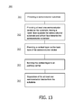
- FIG. 13 schematically shows a method according to embodiments.
- the terms “in ohmic contact”, “in electric contact”, “in contact”, “in ohmic connection”, and “electrically connected” intend to describe that there is an ohmic electric connection or ohmic current path between two regions, portion or parts of a semiconductor device or between different terminals of one or more devices or between a terminal or a metallization and a portion or part of a semiconductor device.
- lateral intends to describe an orientation parallel to a first main surface of a semiconductor substrate.
- vertical as used in this specification intends to describe an orientation, which is arranged perpendicular to the first surface of the semiconductor substrate.
- vertical power semiconductor device shall signify a power semiconductor device in which the drift of charge carriers in the drift zone is vertical, i.e., perpendicular to the first surface of the semiconductor substrate.
- a second surface of a semiconductor substrate is considered to be formed by the lower or back-side surface while the first surface is considered to be formed by the upper, front or main surface of the semiconductor substrate.
- the terms “above”, “upper”, “uppermost”, “over”, “on”, and “below”, “lower” “lowermost”, and “under” as used in this specification therefore describe a relative spatial location of a structural feature to another structural feature with consideration of this orientation.
- the terms “directly above”, “directly over”, “directly on”, “directly below”, “directly under”, “adjacent” and “connecting/connected”, when used with respect to two layers, films, regions, sections, zones or other elements shall signify that these objects contact each other at least physically.
- Embodiments of the present disclosure relate to vertical semiconductor devices, in particular SiC based devices, such as diodes, Schottky diodes, merged pin Schottky diodes, JFETs, MOSFETs, and the like, which are produced in reverse order on a semiconductor substrate comprising SiC.
- SiC based devices such as diodes, Schottky diodes, merged pin Schottky diodes, JFETs, MOSFETs, and the like, which are produced in reverse order on a semiconductor substrate comprising SiC.
- a backside contact is applied to a surface of the semiconductor device opposite the substrate.
- the backside contact is bonded to an auxiliary carrier, and the device is separated from the substrate.
- various methods are employed in embodiments. Examples are an ion implantation into the boundary region between the substrate and the semiconductor device followed by a heating step. This leads to an outgassing of the implanted ions and subsequently to a separation at the boundary region.
- Other separation methods include the application of laser light to the boundary region in order to cause a local overheating leading to a separation.
- Another variant includes the buildup of various layers of SiC with different modifications, such as a porous layer and a monocrystalline layer, which are later separated by a high pressure fluid jet, for example a water jet.
- FIG. 1 illustrates first steps of a manufacturing process of an exemplary semiconductor device 75 , namely a Schottky diode or merged pin Schottky diode according to embodiments.
- Merged pin Schottky diodes or pin diodes may in embodiments comprise pn ⁇ n and pp ⁇ n structures.
- a SiC substrate 10 is provided, onto which a first semiconductor layer 20 comprising SiC, henceforth called first layer 20 , is epitaxially deposited. The border region between the SiC substrate 10 and the semiconductor layer 20 will later form a front face 15 of the semiconductor device 75 manufactured in the process.
- FIG. 2 illustrates that p-doped regions 30 for the lateral termination system of the diode or for a fortification of the anode, as for a merged pin Schottky diode, are implanted into first layer 20 .
- the p-doped regions 30 are subsequently annealed to reduce defects.
- FIG. 3 illustrates the subsequent epitaxial deposition of a second semiconductor layer 40 comprising SiC, henceforth called second layer 40 , having a doping for the drift zone of the semiconductor device.
- the doping rate increases with the duration of the deposition to achieve a field stop.
- the surface of the second layer 40 directed away from the substrate 10 forms a back face 25 of the Schottky diode 75 .
- a cathode contact region is implanted into the second layer 40 .
- the contact region is subsequently annealed, and a metal contact layer 50 is applied to the second layer 40 .
- FIG. 5 illustrates schematically how ions 60 are implanted into the boundary region between the semiconductor substrate 10 and the first layer 20 with a relatively high ion dose per unit area of the targeted material.
- these ions are protons with an energy from 300 keV to 1.5 MeV, more preferably between 500 keV and 1.2 MeV, which are typically applied from the side of the contact layer 50 .
- the ions may alternatively comprise alpha particles.
- the energy of the implantation may be increased compared to protons.
- the implantation energy has to be selected in order to achieve a projected range of the implanted ions to reach at least the depth of the p-doped regions 30 .
- an auxiliary carrier 70 is applied to the metal contact layer 50 .
- the auxiliary carrier may comprise silicon, metal, carbon, ceramics, and glass, or other suitable materials.
- FIG. 6 shows the subsequent separation of the previously produced semiconductor device 75 , which in this embodiment is the Schottky diode, from the SiC substrate 10 by heating. If the applied ion dose is sufficiently chosen, the heating leads to a build-up of hydrogen from the implanted ions 60 , which leads to microbubbles locally destroying the bond between the semiconductor substrate 10 and the semiconductor element 75 produced thereon.
- the separation between the substrate 10 and the semiconductor device 75 may occur not at the exact boundary region between first layer 20 and substrate 10 , but that a thin residual layer 22 of layer 20 may persist on the substrate 10 .
- the exact location of the separation may be influenced by the deposition of the ions 60 into the boundary region. Residual layer 22 is not shown in other Figures for illustrational purposes, though in embodiments it may be present depending on the chosen detailed properties of the separation process.
- the separation may also be executed without the previously described ion implantation, but by applying highly focussed laser light 100 onto the boundary region between semiconductor substrate 10 and the semiconductor device 75 , here the Schottky diode.
- the light leads to a localized overheating of the material in the boundary region between the semiconductor substrate 10 , typically comprising SiC, and the semiconductor device 75 produced as described hereinbefore.
- FIG. 8 the resulting separation of the semiconductor substrate 10 is depicted, leading to the separated semiconductor device 75 together with the auxiliary carrier 70 shown in FIG. 9 .
- FIG. 10 the optional subsequent separation of the auxiliary carrier layer 70 is shown.
- the separation process may also be carried out by building a porous SiC layer 12 on the SiC semiconductor substrate 10 , which is subsequently covered with a monocrystalline SiC layer 14 , on which the semiconductor device 75 is produced.
- the porous SiC layer 12 may be destroyed by a high pressure water jet 110 such as schematically shown in FIG. 12 , leading to the desired separation.
- the front face 15 of the semiconductor device, which is laid open by the separation process, is then typically subject to further processing, which includes at least one of forming a metallization and a passivation. Prior to the metallization, the exposed front face 15 of the semiconductor device may be treated.
- the treatment may comprise mechanical treatments such as polishing, and/or chemical treatment such as etching, and/or a combination of mechanical and chemical treatment such as chemical mechanical polishing (CMP).
- CMP chemical mechanical polishing
- the semiconductor device may optionally be separated from the auxiliary carrier 70 as was shown with respect to FIG. 10 .
- the separated SiC semiconductor substrate 10 may subsequently be reused for a further process cycle producing a further semiconductor device.
- the surface of the substrate may be surface treated prior to the reuse, wherein the treatment may comprise mechanical treatments such as polishing, and/or chemical treatment such as etching, and/or a combination of mechanical and chemical treatment such as chemical mechanical polishing (CMP), and/or an epitaxial deposition step.
- CMP chemical mechanical polishing
- the semiconductor device 75 typically comprising at least one layer comprising SiC, which is produced on the semiconductor substrate 10 , typically comprising SiC, may in embodiments be one of a diode, a Schottky diode as described before, a JFET, and a MOSFET. In some embodiments, the semiconductor device does not comprise a gate oxide.
- the semiconductor substrate 10 may have a thickness from 0.2 mm to 1.0 mm, more preferably from 0.4 mm to 0.8 mm.
- the system of the semiconductor substrate 10 together with the semiconductor device formed thereon is regarded as an intermediate product in the manufacturing process.
- the semiconductor device 75 has a back face 25 opposite the semiconductor substrate 10 and a front face 15 towards the semiconductor substrate 10 , a contact layer 50 on the back face 25 of the semiconductor device 75 , and typically an auxiliary carrier 70 bonded to the contact layer 50 .
- FIG. 13 shows a method 300 for producing a semiconductor device 75 according to embodiments. It includes providing a semiconductor substrate in a block 301 , providing at least one semiconductor device on the substrate, having a back face opposite the semiconductor substrate and a front face towards the semiconductor substrate in a block 302 , providing a contact layer on the back face of the semiconductor device in a block 303 , bonding the contact layer to an auxiliary carrier in a block 304 , and separating the at least one semiconductor device from the substrate in a block 305 .
- Exemplary embodiments of systems and methods for producing a semiconductor device are described above in detail.
- the systems and methods are not limited to the specific embodiments described herein, but rather, components of the systems and/or steps of the methods may be utilized independently and separately from other components and/or steps described herein.
- other types of semiconductor devices may be produced by the described methods, and are not limited to practice with only the semiconductor devices as described herein. Rather, the exemplary embodiment can be implemented and utilized in connection with many other semiconductor devices.
Abstract
A method for producing a semiconductor device is provided. The method includes providing a semiconductor substrate, providing at least one semiconductor device on the substrate, having a back face opposite the semiconductor substrate and a front face towards the semiconductor substrate, providing a contact layer on the back face of the semiconductor device, bonding the contact layer to an auxiliary carrier, and separating the at least one semiconductor device from the substrate. Further, a semiconductor device produced according to the method and an intermediate product are provided.
Description
Embodiments described herein relate to semiconductor devices produced on substrates, in particular to methods for manufacturing such semiconductor devices on substrates comprising SiC.
Semiconductor devices employing SiC are usually expensive due to the high prices of the substrates, which are typically a main factor for the price of the manufactured product. This disadvantage is usually not compensable by other improvements like smaller losses of the product or the like.
There are some concepts pertaining to separating thin layers of SiC from a SiC wafer, to bond them onto carrier plates of carbon or metal, and to bring the resulting layer stack as a whole through the wafer production. Because the original SiC wafer would be reusable, in the case of SiC epitaxial layers even for an unlimited number of cycles, the amount of cost of the basic material could be significantly reduced in this case. However, the carrier stack would have to be able to withstand the high temperatures of the SiC device processing, and there would be no interaction allowed with process chemistry, handling and the like.
In a first aspect, a method for producing a semiconductor device is provided. It includes: providing a semiconductor substrate; providing at least one semiconductor device on the substrate, having a back face opposite the semiconductor substrate and a front face towards the semiconductor substrate; providing a contact layer on the back face of the semiconductor device; bonding the contact layer to an auxiliary carrier; and separating the at least one semiconductor device from the substrate.
According to an embodiment, an intermediate product for the production of a semiconductor device is provided. It includes: a semiconductor substrate, a semiconductor device on the substrate, having a back face opposite the semiconductor substrate and a front face towards the semiconductor substrate, a contact layer on the back face of the semiconductor device, and an auxiliary carrier bonded to the contact layer.
Further aspects, advantages and features of the present invention are apparent from the dependent claims, the description and the accompanying drawings.
A full and enabling disclosure including the best mode thereof, to one of ordinary skill in the art, is set forth more particularly in the remainder of the specification, including reference to the accompanying figures wherein:
The components in the figures are not necessarily to scale, instead emphasis being placed upon illustrating the principles of the invention. Moreover, in the figures, like reference numerals designate corresponding parts.
Reference will now be made in detail to the various embodiments, one or more examples of which are illustrated in each figure. Each example is provided by way of explanation and is not meant as a limitation. For example, features illustrated or described as part of one embodiment can be used on or in conjunction with other embodiments to yield yet further embodiments. It is intended that the present disclosure includes such modifications and variations.
In this regard, directional terminology, such as “top”, “bottom”, “front”, “back”, etc., is used with reference to the orientation of the Figure(s) being described. Because components of embodiments can be positioned in a number of different orientations, the directional terminology is used for purpose of illustration and is in no way limiting. It is to be understood that other embodiments may be utilized and structural or logical changes may be made without departing from the scope of the present invention. The following detailed description, therefore, is not to be taken in a limiting sense, and the scope of the present invention is defined by the appended claims. The embodiments being described use specific language, which should not be construed as limiting the scope of the appended claims. The embodiments can be combined unless noted otherwise. The drawings are not drawn to scale.
In the context of the present specification, the terms “in ohmic contact”, “in electric contact”, “in contact”, “in ohmic connection”, and “electrically connected” intend to describe that there is an ohmic electric connection or ohmic current path between two regions, portion or parts of a semiconductor device or between different terminals of one or more devices or between a terminal or a metallization and a portion or part of a semiconductor device.
The term “lateral” as used in this specification intends to describe an orientation parallel to a first main surface of a semiconductor substrate.
The term “vertical” as used in this specification intends to describe an orientation, which is arranged perpendicular to the first surface of the semiconductor substrate. The term “vertical power semiconductor device” shall signify a power semiconductor device in which the drift of charge carriers in the drift zone is vertical, i.e., perpendicular to the first surface of the semiconductor substrate.
In this specification, a second surface of a semiconductor substrate is considered to be formed by the lower or back-side surface while the first surface is considered to be formed by the upper, front or main surface of the semiconductor substrate. The terms “above”, “upper”, “uppermost”, “over”, “on”, and “below”, “lower” “lowermost”, and “under” as used in this specification therefore describe a relative spatial location of a structural feature to another structural feature with consideration of this orientation. The terms “directly above”, “directly over”, “directly on”, “directly below”, “directly under”, “adjacent” and “connecting/connected”, when used with respect to two layers, films, regions, sections, zones or other elements shall signify that these objects contact each other at least physically.
Embodiments of the present disclosure relate to vertical semiconductor devices, in particular SiC based devices, such as diodes, Schottky diodes, merged pin Schottky diodes, JFETs, MOSFETs, and the like, which are produced in reverse order on a semiconductor substrate comprising SiC. In the end phase of the production process, a backside contact is applied to a surface of the semiconductor device opposite the substrate. Subsequently, the backside contact is bonded to an auxiliary carrier, and the device is separated from the substrate. Thereby, it is made use of the property of SiC that typically, no considerable diffusion of dopants occurs.
For the separation, various methods are employed in embodiments. Examples are an ion implantation into the boundary region between the substrate and the semiconductor device followed by a heating step. This leads to an outgassing of the implanted ions and subsequently to a separation at the boundary region. Other separation methods include the application of laser light to the boundary region in order to cause a local overheating leading to a separation. Another variant includes the buildup of various layers of SiC with different modifications, such as a porous layer and a monocrystalline layer, which are later separated by a high pressure fluid jet, for example a water jet.
In FIG. 4 , a cathode contact region is implanted into the second layer 40. The contact region is subsequently annealed, and a metal contact layer 50 is applied to the second layer 40.
In embodiments schematically illustrated in FIG. 7 , the separation may also be executed without the previously described ion implantation, but by applying highly focussed laser light 100 onto the boundary region between semiconductor substrate 10 and the semiconductor device 75, here the Schottky diode. The light leads to a localized overheating of the material in the boundary region between the semiconductor substrate 10, typically comprising SiC, and the semiconductor device 75 produced as described hereinbefore. In FIG. 8 , the resulting separation of the semiconductor substrate 10 is depicted, leading to the separated semiconductor device 75 together with the auxiliary carrier 70 shown in FIG. 9 .
In FIG. 10 , the optional subsequent separation of the auxiliary carrier layer 70 is shown.
In embodiments illustrated in FIG. 11 , the separation process may also be carried out by building a porous SiC layer 12 on the SiC semiconductor substrate 10, which is subsequently covered with a monocrystalline SiC layer 14, on which the semiconductor device 75 is produced. Instead of the ion 60 or laser induced separation as described before, the porous SiC layer 12 may be destroyed by a high pressure water jet 110 such as schematically shown in FIG. 12 , leading to the desired separation. The front face 15 of the semiconductor device, which is laid open by the separation process, is then typically subject to further processing, which includes at least one of forming a metallization and a passivation. Prior to the metallization, the exposed front face 15 of the semiconductor device may be treated. The treatment may comprise mechanical treatments such as polishing, and/or chemical treatment such as etching, and/or a combination of mechanical and chemical treatment such as chemical mechanical polishing (CMP). The semiconductor device may optionally be separated from the auxiliary carrier 70 as was shown with respect to FIG. 10 .
The separated SiC semiconductor substrate 10 may subsequently be reused for a further process cycle producing a further semiconductor device. In embodiments, the surface of the substrate may be surface treated prior to the reuse, wherein the treatment may comprise mechanical treatments such as polishing, and/or chemical treatment such as etching, and/or a combination of mechanical and chemical treatment such as chemical mechanical polishing (CMP), and/or an epitaxial deposition step.
The semiconductor device 75, typically comprising at least one layer comprising SiC, which is produced on the semiconductor substrate 10, typically comprising SiC, may in embodiments be one of a diode, a Schottky diode as described before, a JFET, and a MOSFET. In some embodiments, the semiconductor device does not comprise a gate oxide.
In embodiments, the semiconductor substrate 10 may have a thickness from 0.2 mm to 1.0 mm, more preferably from 0.4 mm to 0.8 mm.
In the process of manufacturing the semiconductor device 75, the system of the semiconductor substrate 10 together with the semiconductor device formed thereon is regarded as an intermediate product in the manufacturing process. The semiconductor device 75 has a back face 25 opposite the semiconductor substrate 10 and a front face 15 towards the semiconductor substrate 10, a contact layer 50 on the back face 25 of the semiconductor device 75, and typically an auxiliary carrier 70 bonded to the contact layer 50.
Exemplary embodiments of systems and methods for producing a semiconductor device are described above in detail. The systems and methods are not limited to the specific embodiments described herein, but rather, components of the systems and/or steps of the methods may be utilized independently and separately from other components and/or steps described herein. For example, other types of semiconductor devices may be produced by the described methods, and are not limited to practice with only the semiconductor devices as described herein. Rather, the exemplary embodiment can be implemented and utilized in connection with many other semiconductor devices.
Although specific features of various embodiments of the invention may be shown in some drawings and not in others, this is for convenience only. In accordance with the principles of the invention, any feature of a drawing may be referenced and/or claimed in combination with any feature of any other drawing.
This written description uses examples to disclose the invention, including the best mode, and also to enable any person skilled in the art to practice the invention, including making and using any devices or systems and performing any incorporated methods. While various specific embodiments have been disclosed in the foregoing, those skilled in the art will recognize that the spirit and scope of the claims allows for equally effective modifications. Especially, mutually non-exclusive features of the embodiments described above may be combined with each other. The patentable scope of the invention is defined by the claims, and may include other examples that occur to those skilled in the art. Such other examples are intended to be within the scope of the claims if they have structural elements that do not differ from the literal language of the claims, or if they include equivalent structural elements with insubstantial differences from the literal language of the claims.
Claims (23)
1. A method for producing a semiconductor device, comprising:
providing a semiconductor substrate;
providing at least one semiconductor device directly on the substrate, having a back face opposite the semiconductor substrate and a front face directly adjoining the semiconductor substrate, wherein the semiconductor device is at least one of: a diode; a JFET; and a MOSFET,
providing a contact layer on the back face of the semiconductor device;
bonding the contact layer to an auxiliary carrier;
separating the at least one semiconductor device from the substrate; and
separating the semiconductor device from the auxiliary carrier,
wherein the at least one semiconductor device is provided directly on the substrate such that an interface between the semiconductor substrate and the front face of the semiconductor device comprises a junction between two regions which include the same semiconductor material.
2. The method of claim 1 , wherein the semiconductor substrate comprises SiC.
3. The method of claim 1 , wherein the semiconductor device comprises at least one layer comprising SiC.
4. The method of claim 1 , wherein the front face of the semiconductor device is further processed after separation from the semiconductor substrate, wherein the further processing comprises at least one of: forming a metallization; and a passivation.
5. The method of claim 1 , wherein the semiconductor substrate is reused, after separation from the semiconductor device, to produce a further semiconductor device.
6. The method of claim 5 , wherein the semiconductor substrate is surface-treated prior to the reuse.
7. The method of claim 1 , wherein the at least one semiconductor device does not comprise a gate oxide.
8. The method of claim 1 , wherein the auxiliary carrier comprises at least one of the elements selected from the group consisting of: silicon; metal; carbon; ceramics; and glass.
9. The method of claim 1 , wherein separating the at least one semiconductor device from the semiconductor substrate comprises splitting the semiconductor device from the substrate.
10. The method of claim 1 , wherein there is a boundary region between the at least one semiconductor device and the semiconductor substrate, and wherein the separation is carried out by implanting ions into the boundary region and by subsequently heating the boundary region in order to produce gas microbubbles causing the separation.
11. The method of claim 10 , wherein the ions comprise protons.
12. The method of claim 10 , wherein the ions comprise protons, and wherein the implantation energy of the protons is adapted such that the protons are deposited in the boundary region between the at least one semiconductor device and the semiconductor substrate.
13. The method of claim 10 , wherein the ions comprise protons with an energy from 300 keV to 1.5 MeV.
14. The method of claim 1 , wherein separating the at least one semiconductor device from the semiconductor substrate comprises applying laser light through the substrate to the boundary region between the at least one semiconductor device and the semiconductor substrate, in order to achieve a local overheating causing the separation.
15. The method of claim 1 , wherein the semiconductor substrate has a thickness from 0.2 to 1.0 mm.
16. The method of claim 1 , wherein providing at least one semiconductor device comprises:
depositing a first epitaxial layer on the semiconductor substrate;
implanting a dopant into the epitaxial layer; and
depositing a second epitaxial layer on the first epitaxial layer.
17. The method of claim 1 , wherein providing at least one semiconductor device comprises growing a first layer directly on the semiconductor substrate.
18. The method of claim 17 , wherein providing at least one semiconductor device comprises epitaxially growing a first epitaxial layer directly on the semiconductor substrate, wherein a boundary between the first epitaxial layer and the semiconductor substrate forms the front face of the at least one semiconductor device.
19. The method of claim 1 , wherein the substrate comprises an SiC layer, wherein providing the at least one semiconductor device directly on the substrate comprises directly interfacing the SiC layer with the semiconductor device, and wherein separating the at least one semiconductor device from the substrate comprises locally destroying a bond between the SiC layer and the semiconductor device.
20. The method of claim 1 , wherein the semiconductor device includes a single semiconductor material extending from the back face to the front face.
21. The method of claim 20 , wherein the single semiconductor material is SiC-based.
22. The method of claim 1 , wherein the semiconductor material at the junction between two regions is SiC-based.
23. The method of claim 1 , wherein the front face directly adjoining the semiconductor substrate forms a functional layer of the semiconductor device after the separation of the at least one semiconductor device from the substrate.
Priority Applications (4)
| Application Number | Priority Date | Filing Date | Title |
|---|---|---|---|
| US13/791,071 US9875935B2 (en) | 2013-03-08 | 2013-03-08 | Semiconductor device and method for producing the same |
| FR1400487A FR3003086B1 (en) | 2013-03-08 | 2014-02-26 | SEMICONDUCTOR DEVICE AND METHOD FOR MANUFACTURING THE SAME |
| JP2014044272A JP5972922B2 (en) | 2013-03-08 | 2014-03-06 | Semiconductor device and method for manufacturing the same |
| CN201410083341.XA CN104037070B (en) | 2013-03-08 | 2014-03-07 | Semiconductor devices and its production method |
Applications Claiming Priority (1)
| Application Number | Priority Date | Filing Date | Title |
|---|---|---|---|
| US13/791,071 US9875935B2 (en) | 2013-03-08 | 2013-03-08 | Semiconductor device and method for producing the same |
Publications (2)
| Publication Number | Publication Date |
|---|---|
| US20140252373A1 US20140252373A1 (en) | 2014-09-11 |
| US9875935B2 true US9875935B2 (en) | 2018-01-23 |
Family
ID=51409676
Family Applications (1)
| Application Number | Title | Priority Date | Filing Date |
|---|---|---|---|
| US13/791,071 Active 2033-06-08 US9875935B2 (en) | 2013-03-08 | 2013-03-08 | Semiconductor device and method for producing the same |
Country Status (4)
| Country | Link |
|---|---|
| US (1) | US9875935B2 (en) |
| JP (1) | JP5972922B2 (en) |
| CN (1) | CN104037070B (en) |
| FR (1) | FR3003086B1 (en) |
Families Citing this family (10)
| Publication number | Priority date | Publication date | Assignee | Title |
|---|---|---|---|---|
| US11721547B2 (en) | 2013-03-14 | 2023-08-08 | Infineon Technologies Ag | Method for manufacturing a silicon carbide substrate for an electrical silicon carbide device, a silicon carbide substrate and an electrical silicon carbide device |
| DE102017119568B4 (en) * | 2017-08-25 | 2024-01-04 | Infineon Technologies Ag | Silicon carbide components and method for producing silicon carbide components |
| DE102019106124A1 (en) * | 2018-03-22 | 2019-09-26 | Infineon Technologies Ag | Forming semiconductor devices in silicon carbide |
| DE102019111377A1 (en) * | 2018-05-28 | 2019-11-28 | Infineon Technologies Ag | A method of processing a silicon carbide wafer and a silicon carbide semiconductor device |
| DE102018116051A1 (en) * | 2018-07-03 | 2020-01-09 | Infineon Technologies Ag | SEMICONDUCTOR DEVICE AND METHOD FOR PRODUCING A SEMICONDUCTOR DEVICE |
| JPWO2021060366A1 (en) * | 2019-09-27 | 2021-04-01 | ||
| DE102020215007A1 (en) | 2020-11-30 | 2022-06-02 | Robert Bosch Gesellschaft mit beschränkter Haftung | Process for manufacturing a vertical power semiconductor component |
| CN113178383A (en) * | 2021-03-10 | 2021-07-27 | 华为技术有限公司 | Silicon carbide substrate, silicon carbide device and substrate thinning method thereof |
| CN113690183A (en) * | 2021-07-06 | 2021-11-23 | 华为数字能源技术有限公司 | Wafer thinning method |
| WO2023067386A1 (en) * | 2021-10-22 | 2023-04-27 | Infineon Technologies Ag | Manufacturing and reuse of semiconductor substrates |
Citations (18)
| Publication number | Priority date | Publication date | Assignee | Title |
|---|---|---|---|---|
| US6180444B1 (en) * | 1998-02-18 | 2001-01-30 | International Business Machines Corporation | Semiconductor device having ultra-sharp P-N junction and method of manufacturing the same |
| JP2002280531A (en) | 2001-03-19 | 2002-09-27 | Denso Corp | Semiconductor substrate and its manufacturing method |
| CN1427449A (en) | 2001-12-21 | 2003-07-02 | S.O.I.泰克绝缘体硅技术公司 | Technique for transferring thin semiconductor layer and technique for obtaining donor wafer by transferring technique |
| JP2004311955A (en) | 2003-03-25 | 2004-11-04 | Sony Corp | Method for manufacturing very thin electro-optical display device |
| CN1669122A (en) | 2002-01-23 | 2005-09-14 | S.O.I.Tec绝缘体上硅技术公司 | Methods for transferring a useful layer of silicon carbide to a receiving substrate |
| US20060226482A1 (en) | 2005-03-30 | 2006-10-12 | Suvorov Alexander V | Methods of fabricating silicon nitride regions in silicon carbide and resulting structures |
| US20070238263A1 (en) * | 2006-04-06 | 2007-10-11 | Hamza Yilmaz | Method for bonding a semiconductor substrate to a metal substrate |
| US20080038564A1 (en) * | 2003-09-30 | 2008-02-14 | Michel Bruel | Method of Producing a Plate-Shaped Structure, in Particular, From Silicon, Use of Said Method and Plate-Shaped Structure Thus Produced, in Particular From Silicon |
| US20080038902A1 (en) * | 2004-06-21 | 2008-02-14 | Sang-Yun Lee | Semiconductor bonding and layer transfer method |
| JP2009060142A (en) | 2008-12-01 | 2009-03-19 | Sanyo Electric Co Ltd | Nitride semiconductor light emitting device |
| US20110316120A1 (en) | 2006-09-20 | 2011-12-29 | The Board Of Trustees Of The University Of Illinois | Release Strategies for Making Transferable Semiconductor Structures, Devices and Device Components |
| US20120083098A1 (en) | 2010-09-30 | 2012-04-05 | Infineon Technologies Ag | Method for Manufacturing a Composite Wafer Having a Graphite Core, and Composite Wafer Having a Graphite Core |
| US8163581B1 (en) * | 2010-10-13 | 2012-04-24 | Monolith IC 3D | Semiconductor and optoelectronic devices |
| US20120211770A1 (en) * | 2010-05-14 | 2012-08-23 | Sumitomo Electric Industries, Ltd. | Semiconductor device, combined substrate, and methods for manufacturing them |
| JP2012178603A (en) | 2005-09-16 | 2012-09-13 | Cree Inc | Method of processing semiconductor wafer having silicon carbide power device |
| US20120234887A1 (en) * | 2006-09-08 | 2012-09-20 | Silicon Genesis Corporation | Substrate cleaving under controlled stress conditions |
| US20130146936A1 (en) * | 2010-08-03 | 2013-06-13 | Industrial Technology Research Institute | Light emitting diode chip, light emitting diode package structure, and method for forming the same |
| US20140220764A1 (en) * | 2013-02-05 | 2014-08-07 | International Business Machines Corporation | Thin film wafer transfer and structure for electronic devices |
-
2013
- 2013-03-08 US US13/791,071 patent/US9875935B2/en active Active
-
2014
- 2014-02-26 FR FR1400487A patent/FR3003086B1/en active Active
- 2014-03-06 JP JP2014044272A patent/JP5972922B2/en active Active
- 2014-03-07 CN CN201410083341.XA patent/CN104037070B/en active Active
Patent Citations (23)
| Publication number | Priority date | Publication date | Assignee | Title |
|---|---|---|---|---|
| US6180444B1 (en) * | 1998-02-18 | 2001-01-30 | International Business Machines Corporation | Semiconductor device having ultra-sharp P-N junction and method of manufacturing the same |
| JP2002280531A (en) | 2001-03-19 | 2002-09-27 | Denso Corp | Semiconductor substrate and its manufacturing method |
| CN1427449A (en) | 2001-12-21 | 2003-07-02 | S.O.I.泰克绝缘体硅技术公司 | Technique for transferring thin semiconductor layer and technique for obtaining donor wafer by transferring technique |
| US20030153163A1 (en) * | 2001-12-21 | 2003-08-14 | Fabrice Letertre | Support-integrated donor wafers for repeated thin donor layer separation |
| CN1669122A (en) | 2002-01-23 | 2005-09-14 | S.O.I.Tec绝缘体上硅技术公司 | Methods for transferring a useful layer of silicon carbide to a receiving substrate |
| JP2004311955A (en) | 2003-03-25 | 2004-11-04 | Sony Corp | Method for manufacturing very thin electro-optical display device |
| US20080038564A1 (en) * | 2003-09-30 | 2008-02-14 | Michel Bruel | Method of Producing a Plate-Shaped Structure, in Particular, From Silicon, Use of Said Method and Plate-Shaped Structure Thus Produced, in Particular From Silicon |
| US20080038902A1 (en) * | 2004-06-21 | 2008-02-14 | Sang-Yun Lee | Semiconductor bonding and layer transfer method |
| US7718508B2 (en) * | 2004-06-21 | 2010-05-18 | Sang-Yun Lee | Semiconductor bonding and layer transfer method |
| US20060226482A1 (en) | 2005-03-30 | 2006-10-12 | Suvorov Alexander V | Methods of fabricating silicon nitride regions in silicon carbide and resulting structures |
| JP2012178603A (en) | 2005-09-16 | 2012-09-13 | Cree Inc | Method of processing semiconductor wafer having silicon carbide power device |
| US20070238263A1 (en) * | 2006-04-06 | 2007-10-11 | Hamza Yilmaz | Method for bonding a semiconductor substrate to a metal substrate |
| US7635635B2 (en) * | 2006-04-06 | 2009-12-22 | Fairchild Semiconductor Corporation | Method for bonding a semiconductor substrate to a metal substrate |
| US20120234887A1 (en) * | 2006-09-08 | 2012-09-20 | Silicon Genesis Corporation | Substrate cleaving under controlled stress conditions |
| US20110316120A1 (en) | 2006-09-20 | 2011-12-29 | The Board Of Trustees Of The University Of Illinois | Release Strategies for Making Transferable Semiconductor Structures, Devices and Device Components |
| JP2009060142A (en) | 2008-12-01 | 2009-03-19 | Sanyo Electric Co Ltd | Nitride semiconductor light emitting device |
| US20120211770A1 (en) * | 2010-05-14 | 2012-08-23 | Sumitomo Electric Industries, Ltd. | Semiconductor device, combined substrate, and methods for manufacturing them |
| CN102668023A (en) | 2010-05-14 | 2012-09-12 | 住友电气工业株式会社 | Semiconductor device, combined substrate, and methods for manufacturing them |
| US20130146936A1 (en) * | 2010-08-03 | 2013-06-13 | Industrial Technology Research Institute | Light emitting diode chip, light emitting diode package structure, and method for forming the same |
| US20120083098A1 (en) | 2010-09-30 | 2012-04-05 | Infineon Technologies Ag | Method for Manufacturing a Composite Wafer Having a Graphite Core, and Composite Wafer Having a Graphite Core |
| US8163581B1 (en) * | 2010-10-13 | 2012-04-24 | Monolith IC 3D | Semiconductor and optoelectronic devices |
| US20140220764A1 (en) * | 2013-02-05 | 2014-08-07 | International Business Machines Corporation | Thin film wafer transfer and structure for electronic devices |
| US8916451B2 (en) * | 2013-02-05 | 2014-12-23 | International Business Machines Corporation | Thin film wafer transfer and structure for electronic devices |
Also Published As
| Publication number | Publication date |
|---|---|
| JP5972922B2 (en) | 2016-08-17 |
| FR3003086A1 (en) | 2014-09-12 |
| US20140252373A1 (en) | 2014-09-11 |
| CN104037070A (en) | 2014-09-10 |
| FR3003086B1 (en) | 2018-03-16 |
| CN104037070B (en) | 2018-05-04 |
| JP2014179605A (en) | 2014-09-25 |
Similar Documents
| Publication | Publication Date | Title |
|---|---|---|
| US9875935B2 (en) | Semiconductor device and method for producing the same | |
| JP6567118B2 (en) | III-V semiconductor diode | |
| US9601368B2 (en) | Semiconductor device comprising an oxygen diffusion barrier and manufacturing method | |
| EP2320451B1 (en) | Fast recovery Diode | |
| US9793167B2 (en) | Method for forming a wafer structure, a method for forming a semiconductor device and a wafer structure | |
| JP2018082172A (en) | Group iii-v semiconductor diode | |
| CN101861652A (en) | Semiconductor device with (110)-oriented silicon | |
| US7534666B2 (en) | High voltage non punch through IGBT for switch mode power supplies | |
| US20150206758A1 (en) | Method for manufacturing semiconductor device | |
| US20140070265A1 (en) | Fast switching igbt with embedded emitter shorting contacts and method for making same | |
| CN107636806A (en) | The power semiconductor of top-level metallic design with thickness and the method for manufacturing such power semiconductor | |
| JP2023126260A (en) | Silicon carbide component and method for manufacturing the same | |
| CN102832121B (en) | Manufacture method of fast recovery diode | |
| US10249499B2 (en) | Method for manufacturing a semiconductor device comprising a thin semiconductor wafer | |
| US10559664B2 (en) | Method of manufacturing semiconductor device by removing a bulk layer to expose an epitaxial-growth layer and by removing portions of a supporting-substrate to expose portions of the epitaxial-growth layer | |
| US9589926B2 (en) | Method of manufacturing semiconductor device | |
| US20160240380A1 (en) | Method of manufacturing silicon carbide semiconductor device | |
| WO2015035718A1 (en) | Method for preparing fast recovery diode | |
| CN104979161A (en) | Manufacturing method of semiconductor device and manufacturing method of triple mode integrate-insulated gate bipolar transistor (TI-IGBT) | |
| EP4057323B1 (en) | Method for thinning a silicon carbide substrate | |
| JP6570599B2 (en) | Stacked Schottky diode | |
| JP4636685B2 (en) | Diode manufacturing method | |
| JP5301091B2 (en) | Manufacturing method of semiconductor device | |
| JPWO2018055838A1 (en) | Semiconductor device manufacturing method and semiconductor substrate | |
| EP3055884B1 (en) | Systems and methods for bidirectional device fabrication |
Legal Events
| Date | Code | Title | Description |
|---|---|---|---|
| AS | Assignment |
Owner name: INFINEON TECHNOLOGIES AUSTRIA AG, AUSTRIA Free format text: ASSIGNMENT OF ASSIGNORS INTEREST;ASSIGNORS:OTREMBA, RALF;MAUDER, ANTON;SCHULZE, HANS-JOACHIM;SIGNING DATES FROM 20130322 TO 20130325;REEL/FRAME:030626/0495 |
|
| STCF | Information on status: patent grant |
Free format text: PATENTED CASE |
|
| MAFP | Maintenance fee payment |
Free format text: PAYMENT OF MAINTENANCE FEE, 4TH YEAR, LARGE ENTITY (ORIGINAL EVENT CODE: M1551); ENTITY STATUS OF PATENT OWNER: LARGE ENTITY Year of fee payment: 4 |