US9866018B2 - System and method for transistor voltage control - Google Patents
System and method for transistor voltage control Download PDFInfo
- Publication number
- US9866018B2 US9866018B2 US14/920,672 US201514920672A US9866018B2 US 9866018 B2 US9866018 B2 US 9866018B2 US 201514920672 A US201514920672 A US 201514920672A US 9866018 B2 US9866018 B2 US 9866018B2
- Authority
- US
- United States
- Prior art keywords
- gate
- voltage
- load
- buffer
- transistor
- Prior art date
- Legal status (The legal status is an assumption and is not a legal conclusion. Google has not performed a legal analysis and makes no representation as to the accuracy of the status listed.)
- Active, expires
Links
Images


Classifications
-
- H—ELECTRICITY
- H03—ELECTRONIC CIRCUITRY
- H03K—PULSE TECHNIQUE
- H03K17/00—Electronic switching or gating, i.e. not by contact-making and –breaking
- H03K17/08—Modifications for protecting switching circuit against overcurrent or overvoltage
- H03K17/082—Modifications for protecting switching circuit against overcurrent or overvoltage by feedback from the output to the control circuit
- H03K17/0822—Modifications for protecting switching circuit against overcurrent or overvoltage by feedback from the output to the control circuit in field-effect transistor switches
-
- H—ELECTRICITY
- H02—GENERATION; CONVERSION OR DISTRIBUTION OF ELECTRIC POWER
- H02J—CIRCUIT ARRANGEMENTS OR SYSTEMS FOR SUPPLYING OR DISTRIBUTING ELECTRIC POWER; SYSTEMS FOR STORING ELECTRIC ENERGY
- H02J1/00—Circuit arrangements for dc mains or dc distribution networks
-
- H—ELECTRICITY
- H02—GENERATION; CONVERSION OR DISTRIBUTION OF ELECTRIC POWER
- H02M—APPARATUS FOR CONVERSION BETWEEN AC AND AC, BETWEEN AC AND DC, OR BETWEEN DC AND DC, AND FOR USE WITH MAINS OR SIMILAR POWER SUPPLY SYSTEMS; CONVERSION OF DC OR AC INPUT POWER INTO SURGE OUTPUT POWER; CONTROL OR REGULATION THEREOF
- H02M1/00—Details of apparatus for conversion
- H02M1/08—Circuits specially adapted for the generation of control voltages for semiconductor devices incorporated in static converters
Definitions
- the present disclosure generally relates to powering loads with load-switcher circuitry, and more particularly relates to controlling transistor voltages in load-switcher circuitry.
- Information handling systems generally process, compile, store, and/or communicate information or data for business, personal, or other purposes. Because technology and information handling needs and requirements vary between different applications, information handling systems may also vary regarding what information is handled, how the information is processed, stored, or communicated, and how quickly and efficiently the information may be processed, stored, or communicated. The variations in information handling systems allow information handling systems to be general purpose systems or to be configured for specific uses or users, such as for financial transaction or reservation processing, for enterprise data storage, for global communications, or for other specific uses or users. In addition, information handling systems may include a variety of hardware and software resources that may be configured to process, store, and communicate information and may include one or more computer systems, data storage systems, and networking systems.
- Voltage regulators may be used in integrated circuits or other circuitry to power loads.
- control circuitry can be used to control a set of voltage regulators to power a corresponding set of loads.
- FIG. 1 is a schematic diagram of an embodiment of a voltage regulator system for powering loads
- FIG. 2 is a schematic diagram of an embodiment of a voltage regulator system with load-switcher circuitry
- FIGS. 3 a -3 e are circuit diagrams of an embodiment of load-switcher circuitry at different stages of operation
- FIG. 4 is a graph of transistor voltages according to an embodiment
- FIG. 5 is a graph of voltage waveforms according to an embodiment.
- FIG. 1 illustrates an information handling system 100 in which a set of voltage regulators are used to power a set of loads.
- an information handling system can include any instrumentality or aggregate of instrumentalities operable to compute, classify, process, transmit, receive, retrieve, originate, switch, store, display, manifest, detect, record, reproduce, handle, or utilize any form of information, intelligence, or data for business, scientific, control, entertainment, or other purposes.
- an information handling system can be a personal computer, a laptop computer, a smart phone, a tablet device or other consumer electronic device, a network server, a network storage device, a switch router or other network communication device, or any other suitable device and may vary in size, shape, performance, functionality, and price.
- an information handling system can include processing resources for executing machine-executable code, such as a central processing unit (CPU), a programmable logic array (PLA), an embedded device such as a System-on-a-Chip (SoC), or other control logic hardware.
- An information handling system can also include one or more computer-readable medium for storing machine-executable code, such as software or data.
- Additional components of an information handling system can include one or more storage devices that can store machine-executable code, one or more communications ports for communicating with external devices, and various input and output (I/O) devices, such as a keyboard, a mouse, and a video display.
- I/O input and output
- An information handling system can also include one or more buses operable to transmit information between the various hardware components.
- the output voltages and power of the voltage regulators may be similar within a threshold to power the loads.
- loads 106 and 116 may require the same (maximum, or minimum) or similar voltage and power to be provided by voltage regulators 105 and 115 .
- load-switcher circuitry may be used with a voltage regulator to eliminate the need for a further voltage regulator to power a further load.
- FIG. 2 illustrates a system 200 using load-switcher circuitry instead of a further voltage regulator to power a further load.
- voltage regulator 115 has been replaced with load-switcher circuitry 215 .
- system 200 comprises control circuitry 102 , voltage regulator 105 , load-switcher circuitry 215 , and loads 106 and 116 .
- control circuitry 102 controls voltage regulator 105 via control signals 103 a to power corresponding load 106 , and to also power load-switcher circuitry 215 .
- Control circuitry 102 further controls load-switcher circuitry 215 via control signals 203 to power load 116 .
- system 200 includes a single voltage regulator providing power to load 106 and load-switcher circuitry 215 —which replaces voltage regulator 115 of system 100 to provide power to load 116 .
- Load-switcher circuitry generally include one or more transistors, such as a Field Effect Transistor (FET), which may be implemented, for example, as a metal oxide semiconductor FET (MOSFET).
- FET Field Effect Transistor
- MOSFET metal oxide semiconductor FET
- the MOSFET component may occupy a relatively large portion of the area of the load-switcher circuitry. Thus, it may be desired to minimize the relative size of the MOSFET in the load-switcher circuitry.
- a physical MOSFET coupled in a circuit empirically has a source-drain resistance and three parasitic capacitances: a parasitic capacitance between source and drain, a parasitic capacitance between gate and drain, and a parasitic capacitance between gate and source.
- a physical MOSFET will have voltages corresponding to each of the parasitic capacitances. Gate-source voltage fluctuations and the maximum values thereof strain a MOSFET, and the MOSFET must be sized large enough to handle maximum gate-source voltage swings.
- the Miller effect may be leveraged to reduce the voltage stress on the MOSFET by controlling the voltage and power applied to the MOSFET in the load-switcher circuitry.
- an external buffer may be connected between drain and gate to control the MOSFET on/off speed.
- a slow gate charge circuit may be implemented in the load switcher circuitry relative to the MOSFET (and the gate of the MOSFET), to control gate-source voltage parameters of the MOSFET.
- voltage stress on the MOSFET may be reduced by controlling the timing of applying a voltage supply to the MOSFET.
- the supply voltage could be applied to the MOSFET at an earlier time than otherwise.
- an external buffer, a slow gate charge circuit, and controlled temporal application of the supply voltage to a MOSFET may be used to reduce the voltage stress on the MOSFET.
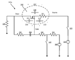
- FIG. 3 a illustrates an example of load-switcher circuitry 300 a utilizing a MOSFET 310 .
- Load-switcher circuitry 300 a includes load 320 (illustrated as a resistor to indicate power loss) and voltage supply 322 , which corresponds to the voltage output of voltage regulator 105 of system 200 .
- the drain of MOSFET 310 is coupled to load 320 .
- voltage supply 322 is coupled to the source of MOSFET 310 via switch 323 which may be opened or closed to connect or disconnect the voltage output of voltage supply 322 with the source of MOSFET 310 .
- Resistor 332 and capacitor 334 form a buffer or part of a buffer to control MOSFET 310 on/off speed. Resistor 332 and capacitor 334 are connected in series (between gate and drain). As illustrated, capacitor 334 is connected to the gate of MOSFET 310 and resistor 332 is connected to the drain of MOSFET 310 . Resistors 344 and 346 together with switch 345 form a slow gate charge circuit or part of a slow gate charge circuit. Control voltage 342 corresponds to control signals 203 of system 200 and is connected to the gate of MOSFET 310 via resistors 344 and 346 , which are connected in series.
- resistor 344 One end of resistor 344 is coupled to control voltage 342 , while the antipodal end of resistor 344 is coupled to switch 345 which is configured to be operable to short the voltage output of control voltage 342 to ground via resistor 344 , thereby allowing for controlled application of voltage from control voltage 342 to control the gate of MOSFET 310 .
- Resistor 346 is coupled to the antipodal end of resistor 344 , and to the gate of MOSFET 310 , thereby coupling resistor 344 to the gate.
- MOSFET 310 has a source, drain, and controlling gate, as labeled in system 300 a .
- MOSFET 310 is a p-type FET with an active-off gate control voltage.
- MOSFET 310 has an inherent resistance from source to drain, illustrated as resistor 311 .
- MOSFET 310 further has parasitic capacitances 312 , 314 , and 316 .
- Capacitance 312 is the parasitic capacitance between gate and source.
- Capacitance 314 is the parasitic capacitance between gate and drain.
- capacitance 316 is the parasitic capacitance between drain and source.
- the respective resistances of resistors 344 and 346 are selected for charging and discharging parasitic capacitances 312 and 314 (the parasitic capacitances associated with the gate of MOSFET 310 ). More particularly, since resistors 344 and 346 are in series between the gate of MOSFET 310 and control voltage 342 , the effective resistance of the combination of resistors 344 and 346 slow the application of voltage from control voltage 342 to the gate of MOSFET 310 , thereby slowing the charging of capacitances 312 and 314 by control voltage 342 .
- Switch 345 uses shorting control voltage 342 to control the application of voltage from control voltage 342 to the gate of MOSFET 310 . When switch 345 is electrically connected to ground, parasitic capacitances 312 and 314 discharge through resistor 346 to ground.
- control voltage 342 is electrically coupled to the gate of MOSFET 310 via resistors 344 and 346 , and the voltage of control voltage 342 charges capacitances 312 and 314 , as well as capacitor 334 (allowing for the resistance values of resistors 344 and 346 to affect a rate of charge of capacitances 312 and 314 ). Furthermore, since capacitor 334 is also simultaneously charging along with charging capacitances 312 and 314 , the capacitance value of capacitor 334 affects the rate of charge of capacitances 312 and 314 .
- control voltage 342 is electrically decoupled from the gate of MOSFET 310 because control voltage 342 is shorted to ground via resistor 344 .
- switch 345 is operated to connect resistor 344 to ground, as illustrated in FIG. 3 a , one end of resistor 346 will also be shorted to the ground, and parasitic capacitances 312 and 314 will be connected to ground, and charge from parasitic capacitances 312 and 314 will flow to the ground via resistor 346 and switch 345 .
- the resistance value of resistor 346 controls the rate of discharge of capacitances 312 and 314 .
- capacitor 334 is coupled to the gate of MOSFET 310 and helps to control the rate of discharge of capacitances 312 and 314 , because as shown in FIG. 3 a , capacitor 334 is coupled to resistor 346 in parallel with parasitic capacitances 312 and 314 , and as such, when charged, provides a voltage potential that must flow through resistor 346 to ground, thereby affecting, for example, slowing, the rate of discharge of capacitances 312 and 314 .
- switch 323 may be controlled by control circuitry to control the temporal application of voltage of voltage supply 322 to MOSFET 310 .
- control circuitry may be configured to cause switch 323 to couple voltage supply 322 to MOSFET 310 earlier than otherwise to reduce the overall voltage stress on MOSFET 310 and reduce the relative resistance of resistor 311 (the drain-source resistance).
- FIGS. 3 b -3 e are equivalent circuit diagrams to system 300 a of FIG. 3 a at different temporal stages of operation of system 300 a .
- FIG. 4 provides a graph 400 of the voltages across capacitances 312 , 314 , and 316 at different temporal stages of operation of system 300 a , and will be discussed in conjunction with FIGS. 3 a - 3 e.
- System 300 b of FIG. 3 b is the equivalent circuit to system 300 a when voltage supply 322 is disconnected from system 300 a by switch 323 (or the voltage regulator 105 is turned off via control circuitry 102 as shown in 200 ), control voltage 342 is not shorted to ground by switch 345 and resistor 344 , and MOSFET 310 is going to off (due to the application of control voltage 342 ).
- This state is illustrated in FIG. 4 from 10-20 milliseconds (mS). In this state, charge from control voltage 342 flows though resistances 344 and 346 to charge parasitic capacitances 312 and 314 , and a corresponding voltage is applied to parasitic capacitances 312 and 314 as illustrated by the rising voltages 313 and 315 of graph 400 .
- Control voltage 342 is disjoint with regard parasitic capacitance 316 and there is not voltage potential formed by control voltage 342 with regard to parasitic capacitance 316 , and therefore voltage 317 is zero, as illustrated from 10-20 milliseconds of graph 400 .
- the combination of resistors 344 and 346 slow the increase of voltage 313 (gate-source voltage), and pull down the voltage value of control voltage 342 , thereby helping to reduce voltage 313 over the illustrated 10-20 milliseconds of graph 400 .
- System 300 c of FIG. 3 c is the equivalent circuit to system 300 a when voltage supply 322 is connected to system 300 a by switch 323 (more particularly, the source of MOSFET 310 ) and control voltage 342 is not shorted to ground by switch 345 (and therefore control voltage 342 is applied to the gate of MOSFET 310 , ensuring that MOSFET 310 is off).
- This state is illustrated in FIG. 4 from 20-100 milliseconds (mS).
- voltage 313 the gate source voltage of MOSFET 310
- voltage 313 increases asymptotic to a voltage value as in graph 400 .
- the voltage applied to parasitic capacitance 312 drops to control voltage 342 minus voltage 322 , then rises asymptotic to a voltage.
- voltage 315 continues to increase asymptotic to the voltage value of voltage supply 322 such that parasitic capacitance 314 charges to the voltage value of voltage supply 322 . This is shown by the rising asymptotic voltage 315 of graph 400 . Simultaneously, voltage 317 drops to a negative value, as illustrated in graph 400 .
- System 300 d of FIG. 3 d is the equivalent circuit to system 300 a when voltage supply 322 is connected to system 300 a by switch 323 (more particularly, the source of MOSFET 310 ) and control voltage 342 is shorted to ground by switch 345 , thereby removing the voltage of control voltage 342 from the gate of MOSFET 310 .
- This state is illustrated in FIG. 4 from 100-160 milliseconds (mS). Since MOSFET 310 is an active control P-type FET, the control voltage is 342 is no longer applied to the gate of MOSFET 310 , but is shorted to ground, MOSFET 310 turns on and a channel resistance 311 is formed between drain and source.
- voltage 317 rises from the negative voltage value to zero as MOSFET 310 turns on and the channel between the source and drain becomes active.
- the opening of the channel reduces parasitic capacitance 316 (between source and drain) to zero such that voltage 717 across parasitic capacitance 316 asymptotes to zero.
- System 300 e of FIG. 3 e is the equivalent circuit to system 300 a when voltage supply 322 is connected to system 300 a by switch 323 (more particularly, the source of MOSFET 310 ) and control voltage 342 is not shorted to ground by switch 345 , and therefore a voltage is applied to the gate of MOSFET 310 .
- This state is illustrated in FIG. 4 from 160 milliseconds (mS) forth.
- MOSFET 310 is an active control P-type FET, and since control voltage is 342 is applied to the gate of MOSFET 310 , and is no longer shorted to ground, MOSFET 310 is turning off and the channel between drain and source is fading.
- voltage 317 drops below zero as the channel between source and drain fades, and parasitic capacitance 316 (between source and drain) forms which is negatively charged by the combination of control voltage 342 and voltage supply 322 .
- voltages 313 and 315 rise from the negative voltage value to asymptote different final voltages.
- the voltage combination of control voltage 342 and voltage supple 322 are applied to parasitic capacitances 312 and 314 (the parasitic capacitances associated with the gate of MOSFET 310 ) to charge parasitic capacitances 312 and 314 via resistors 344 and 346 such that the resistor values of resistors 344 and 346 affect the rate of charge of parasitic capacitances 312 and 314 .
- the resistance values of resistors 344 and 346 may be selected to control a rate of charge of parasitic capacitances 312 and 314 .
- voltage 315 rises asymptotic to the voltage of voltage supply 322
- voltage 313 is asymptotic to a lower voltage value.
- the value of resistor 344 may be 5.9 kOhms and the value of resistor 346 may be 2.2 kOhms.
- the maximum voltage of control voltage 342 may be 12 volts and the voltage of supply voltage 322 may be 5 volts.
- Embodiments described above have numerous advantages. For example, embodiments of the mechanism described above allow for less voltage stress on a transistor by means of the extra resistor-capacitor buffer and resistor based timing control of the on/off of the transistor. This mechanism does not require a further big MOSFET rating. Further, the buffer capacitor may be within a twenty percent margin of ten times the capacitance of the combined parasitic capacitances of the gate and may help compensate the parasitic capacitance of the transistor. This further helps prevent a spike current exceeding the system specification. Further the above-described transistor based system helps to improve efficiency. In addition, the lower voltage applied to the transistor in embodiments of the transistor mechanism described herein results in a lower source drain resistance, and therefore a smaller transistor may be used in a system. Embodiments further allow for the voltage control circuitry to reduce power stress on the transistor. Furthermore, embodiments mitigate power supply dip when load-switcher circuitry transitions between on and off.
- FIG. 5 illustrates waveforms 500 exemplifying advantages of embodiments of mechanism and systems disclosed herein.
- Waveform 510 is a graph of the voltage applied to the gate-source of a transistor of load-switcher circuitry lacking an external buffer and slow gate charge circuit.
- waveform 510 is a graph of the voltage applied to the gate-source of a transistor of load-switcher circuitry without changing the temporal application of the supply voltage to the transistor.
- the maximum voltage approaches the supply voltage and as such may exceed a maximum transistor safe voltage, as illustrated.
- Waveform 520 is a graph of the voltage applied to the gate-source of a transistor of load-switcher circuitry including an external buffer and slow gate charge circuit.
- waveform 520 is a graph of the voltage applied to the gate-source of a transistor of load-switcher circuitry in which the temporal timing of the application of the supply voltage to the transistor is changed. As can be seen from waveform 520 , the maximum voltage is maintained within a maximum transistor safe voltage, as illustrated.
- Waveform 515 and 516 illustrate the supply voltage as applied to the source of a load-switcher circuit transistor with different temporal timings.
- Waveform 515 is a graph of the application of the supply voltage to the transistor without changing the temporal application of the supply voltage to the transistor.
- the supply voltage is applied to the transistor when the prior voltage rail is stable, for example that Vgs 313 be charged as control voltage 342 .
- waveform 510 which illustrates the effects of the temporal application of the supply voltage as delineated by waveform 515 , the gate source voltage immediately drops into the safe area when the supply voltage is applied to the transistor.
- Waveform 516 (the dashed waveform superimposed on waveform 515 ) is a graph of the application of the supply voltage to the transistor with changing the temporal application of the supply voltage to the transistor. More particularly, the temporal application of the supply voltage to the transistor may be brought forward as illustrated by waveform 516 increasing to the supply voltage prior to waveform 515 . Referring to waveform 520 which illustrates the effects of the temporal application of the supply voltage as delineated by waveform 516 , the gate source voltage is brought down sooner compared to waveform 510 . This helps mitigate voltage stress on the transistor. The temporal application of the supply voltage to the transistor may be determined by a desired slow charging duration of Vgs 313 .
Landscapes
- Engineering & Computer Science (AREA)
- Power Engineering (AREA)
- Electronic Switches (AREA)
Abstract
Description
Claims (19)
Priority Applications (1)
| Application Number | Priority Date | Filing Date | Title |
|---|---|---|---|
| US14/920,672 US9866018B2 (en) | 2015-10-22 | 2015-10-22 | System and method for transistor voltage control |
Applications Claiming Priority (1)
| Application Number | Priority Date | Filing Date | Title |
|---|---|---|---|
| US14/920,672 US9866018B2 (en) | 2015-10-22 | 2015-10-22 | System and method for transistor voltage control |
Publications (2)
| Publication Number | Publication Date |
|---|---|
| US20170117706A1 US20170117706A1 (en) | 2017-04-27 |
| US9866018B2 true US9866018B2 (en) | 2018-01-09 |
Family
ID=58559169
Family Applications (1)
| Application Number | Title | Priority Date | Filing Date |
|---|---|---|---|
| US14/920,672 Active 2036-07-07 US9866018B2 (en) | 2015-10-22 | 2015-10-22 | System and method for transistor voltage control |
Country Status (1)
| Country | Link |
|---|---|
| US (1) | US9866018B2 (en) |
Families Citing this family (1)
| Publication number | Priority date | Publication date | Assignee | Title |
|---|---|---|---|---|
| US11199894B2 (en) * | 2018-10-30 | 2021-12-14 | Dell Products L.P. | Method and apparatus for providing high bandwidth capacitor circuit in power assist unit |
Citations (8)
| Publication number | Priority date | Publication date | Assignee | Title |
|---|---|---|---|---|
| US6903597B2 (en) | 2003-01-21 | 2005-06-07 | Toshiba Mitsubishi-Electric Industrial Systems Corporation | Gate driving circuit |
| US20060012354A1 (en) * | 2004-07-13 | 2006-01-19 | Fujitsu Limited | Step-down circuit |
| US20090059630A1 (en) * | 2006-12-30 | 2009-03-05 | Advanced Analogic Technologies, Inc. | High-efficiency DC/DC voltage converter including capacitive switching pre-converter and down inductive switching post-regulator |
| US7952418B2 (en) | 2008-06-27 | 2011-05-31 | Dell Products L.P. | Enhanced transistor gate drive |
| US20120098511A1 (en) | 2009-04-29 | 2012-04-26 | Dell Products, L.P. | Systems and methods for intelligently optimizing operating efficiency using variable gate drive voltage |
| US20140266323A1 (en) * | 2013-03-14 | 2014-09-18 | Allegro Microsystems, Inc. | Systems and Methods for Driving a Load Under Various Power Conditions |
| US20160091909A1 (en) * | 2014-09-30 | 2016-03-31 | Analog Devices, Inc. | Soft start circuit and method for dc-dc voltage regulator |
| US20170018220A1 (en) * | 2014-03-13 | 2017-01-19 | Joled Inc. | El display apparatus |
-
2015
- 2015-10-22 US US14/920,672 patent/US9866018B2/en active Active
Patent Citations (8)
| Publication number | Priority date | Publication date | Assignee | Title |
|---|---|---|---|---|
| US6903597B2 (en) | 2003-01-21 | 2005-06-07 | Toshiba Mitsubishi-Electric Industrial Systems Corporation | Gate driving circuit |
| US20060012354A1 (en) * | 2004-07-13 | 2006-01-19 | Fujitsu Limited | Step-down circuit |
| US20090059630A1 (en) * | 2006-12-30 | 2009-03-05 | Advanced Analogic Technologies, Inc. | High-efficiency DC/DC voltage converter including capacitive switching pre-converter and down inductive switching post-regulator |
| US7952418B2 (en) | 2008-06-27 | 2011-05-31 | Dell Products L.P. | Enhanced transistor gate drive |
| US20120098511A1 (en) | 2009-04-29 | 2012-04-26 | Dell Products, L.P. | Systems and methods for intelligently optimizing operating efficiency using variable gate drive voltage |
| US20140266323A1 (en) * | 2013-03-14 | 2014-09-18 | Allegro Microsystems, Inc. | Systems and Methods for Driving a Load Under Various Power Conditions |
| US20170018220A1 (en) * | 2014-03-13 | 2017-01-19 | Joled Inc. | El display apparatus |
| US20160091909A1 (en) * | 2014-09-30 | 2016-03-31 | Analog Devices, Inc. | Soft start circuit and method for dc-dc voltage regulator |
Also Published As
| Publication number | Publication date |
|---|---|
| US20170117706A1 (en) | 2017-04-27 |
Similar Documents
| Publication | Publication Date | Title |
|---|---|---|
| TWI769160B (en) | Method, circuitry, and electronic system to soft start high power charge pumps | |
| US9236866B2 (en) | Circuit for driving gate of power MOS transistor | |
| US9348383B2 (en) | Apparatus for starting up switching voltage regulator | |
| US9459639B2 (en) | Power supply circuit with control unit | |
| US10727730B2 (en) | Increasing efficiency of a switched mode power converter | |
| US20130176008A1 (en) | Soft Start Circuit and Power Supply Device Using the Same | |
| CN105449998A (en) | Circuit and method for driver control of switching circuit | |
| US10666137B2 (en) | Method and circuitry for sensing and controlling a current | |
| JP2017168924A (en) | Semiconductor device | |
| US20140098582A1 (en) | Bridge rectifier circuit | |
| US10187055B2 (en) | Output discharge techniques for load switches | |
| US9866018B2 (en) | System and method for transistor voltage control | |
| US9559583B2 (en) | Power converter with a wave generator that filters a wave signal to generate an output voltage | |
| US8854097B2 (en) | Load switch | |
| US20070052446A1 (en) | Driver circuit | |
| US9059703B2 (en) | Switch circuit | |
| US8207755B1 (en) | Low leakage power detection circuit | |
| CN212627662U (en) | Driver circuit and driver | |
| CN106027013B (en) | Control device and control method for analog power switch | |
| US9853636B2 (en) | Semiconductor apparatus | |
| US9467122B2 (en) | Switching scheme to extend maximum input voltage range of a DC-to-DC voltage converter | |
| US9287856B2 (en) | Tracking circuit | |
| JP5750326B2 (en) | Electronic device protection circuit |
Legal Events
| Date | Code | Title | Description |
|---|---|---|---|
| AS | Assignment |
Owner name: BANK OF AMERICA, N.A., AS ADMINISTRATIVE AGENT, NO Free format text: SUPPLEMENTAL PATENT SECURITY AGREEMENT - ABL;ASSIGNORS:DELL PRODUCTS L.P.;DELL SOFTWARE INC.;BOOMI, INC.;AND OTHERS;REEL/FRAME:037160/0171 Effective date: 20151124 Owner name: BANK OF AMERICA, N.A., AS COLLATERAL AGENT, NORTH Free format text: SUPPLEMENTAL PATENT SECURITY AGREEMENT - TERM LOAN;ASSIGNORS:DELL PRODUCTS L.P.;DELL SOFTWARE INC.;BOOMI, INC.;AND OTHERS;REEL/FRAME:037160/0239 Effective date: 20151124 Owner name: THE BANK OF NEW YORK MELLON TRUST COMPANY, N.A., A Free format text: SUPPLEMENTAL PATENT SECURITY AGREEMENT - NOTES;ASSIGNORS:DELL PRODUCTS L.P.;DELL SOFTWARE INC.;BOOMI, INC.;AND OTHERS;REEL/FRAME:037160/0142 Effective date: 20151124 Owner name: BANK OF AMERICA, N.A., AS COLLATERAL AGENT, NORTH CAROLINA Free format text: SUPPLEMENTAL PATENT SECURITY AGREEMENT - TERM LOAN;ASSIGNORS:DELL PRODUCTS L.P.;DELL SOFTWARE INC.;BOOMI, INC.;AND OTHERS;REEL/FRAME:037160/0239 Effective date: 20151124 Owner name: THE BANK OF NEW YORK MELLON TRUST COMPANY, N.A., AS FIRST LIEN COLLATERAL AGENT, TEXAS Free format text: SUPPLEMENTAL PATENT SECURITY AGREEMENT - NOTES;ASSIGNORS:DELL PRODUCTS L.P.;DELL SOFTWARE INC.;BOOMI, INC.;AND OTHERS;REEL/FRAME:037160/0142 Effective date: 20151124 Owner name: BANK OF AMERICA, N.A., AS ADMINISTRATIVE AGENT, NORTH CAROLINA Free format text: SUPPLEMENTAL PATENT SECURITY AGREEMENT - ABL;ASSIGNORS:DELL PRODUCTS L.P.;DELL SOFTWARE INC.;BOOMI, INC.;AND OTHERS;REEL/FRAME:037160/0171 Effective date: 20151124 |
|
| AS | Assignment |
Owner name: WYSE TECHNOLOGY L.L.C., CALIFORNIA Free format text: RELEASE OF REEL 037160 FRAME 0171 (ABL);ASSIGNOR:BANK OF AMERICA, N.A., AS ADMINISTRATIVE AGENT;REEL/FRAME:040017/0253 Effective date: 20160907 Owner name: DELL PRODUCTS L.P., TEXAS Free format text: RELEASE OF REEL 037160 FRAME 0171 (ABL);ASSIGNOR:BANK OF AMERICA, N.A., AS ADMINISTRATIVE AGENT;REEL/FRAME:040017/0253 Effective date: 20160907 Owner name: DELL SOFTWARE INC., CALIFORNIA Free format text: RELEASE OF REEL 037160 FRAME 0171 (ABL);ASSIGNOR:BANK OF AMERICA, N.A., AS ADMINISTRATIVE AGENT;REEL/FRAME:040017/0253 Effective date: 20160907 |
|
| AS | Assignment |
Owner name: WYSE TECHNOLOGY L.L.C., CALIFORNIA Free format text: RELEASE OF REEL 037160 FRAME 0142 (NOTE);ASSIGNOR:BANK OF NEW YORK MELLON TRUST COMPANY, N.A., AS COLLATERAL AGENT;REEL/FRAME:040027/0812 Effective date: 20160907 Owner name: DELL SOFTWARE INC., CALIFORNIA Free format text: RELEASE OF REEL 037160 FRAME 0239 (TL);ASSIGNOR:BANK OF AMERICA, N.A., AS COLLATERAL AGENT;REEL/FRAME:040028/0115 Effective date: 20160907 Owner name: DELL PRODUCTS L.P., TEXAS Free format text: RELEASE OF REEL 037160 FRAME 0239 (TL);ASSIGNOR:BANK OF AMERICA, N.A., AS COLLATERAL AGENT;REEL/FRAME:040028/0115 Effective date: 20160907 Owner name: DELL SOFTWARE INC., CALIFORNIA Free format text: RELEASE OF REEL 037160 FRAME 0142 (NOTE);ASSIGNOR:BANK OF NEW YORK MELLON TRUST COMPANY, N.A., AS COLLATERAL AGENT;REEL/FRAME:040027/0812 Effective date: 20160907 Owner name: DELL PRODUCTS L.P., TEXAS Free format text: RELEASE OF REEL 037160 FRAME 0142 (NOTE);ASSIGNOR:BANK OF NEW YORK MELLON TRUST COMPANY, N.A., AS COLLATERAL AGENT;REEL/FRAME:040027/0812 Effective date: 20160907 Owner name: WYSE TECHNOLOGY L.L.C., CALIFORNIA Free format text: RELEASE OF REEL 037160 FRAME 0239 (TL);ASSIGNOR:BANK OF AMERICA, N.A., AS COLLATERAL AGENT;REEL/FRAME:040028/0115 Effective date: 20160907 |
|
| AS | Assignment |
Owner name: CREDIT SUISSE AG, CAYMAN ISLANDS BRANCH, AS COLLAT Free format text: SECURITY AGREEMENT;ASSIGNORS:ASAP SOFTWARE EXPRESS, INC.;AVENTAIL LLC;CREDANT TECHNOLOGIES, INC.;AND OTHERS;REEL/FRAME:040134/0001 Effective date: 20160907 Owner name: THE BANK OF NEW YORK MELLON TRUST COMPANY, N.A., A Free format text: SECURITY AGREEMENT;ASSIGNORS:ASAP SOFTWARE EXPRESS, INC.;AVENTAIL LLC;CREDANT TECHNOLOGIES, INC.;AND OTHERS;REEL/FRAME:040136/0001 Effective date: 20160907 Owner name: CREDIT SUISSE AG, CAYMAN ISLANDS BRANCH, AS COLLATERAL AGENT, NORTH CAROLINA Free format text: SECURITY AGREEMENT;ASSIGNORS:ASAP SOFTWARE EXPRESS, INC.;AVENTAIL LLC;CREDANT TECHNOLOGIES, INC.;AND OTHERS;REEL/FRAME:040134/0001 Effective date: 20160907 Owner name: THE BANK OF NEW YORK MELLON TRUST COMPANY, N.A., AS NOTES COLLATERAL AGENT, TEXAS Free format text: SECURITY AGREEMENT;ASSIGNORS:ASAP SOFTWARE EXPRESS, INC.;AVENTAIL LLC;CREDANT TECHNOLOGIES, INC.;AND OTHERS;REEL/FRAME:040136/0001 Effective date: 20160907 |
|
| AS | Assignment |
Owner name: DELL PRODUCTS, LP, TEXAS Free format text: ASSIGNMENT OF ASSIGNORS INTEREST;ASSIGNORS:YU, WICKMAN (FENG-YU);CHEN, VINCENT (CHIA HUNG);SIGNING DATES FROM 20151022 TO 20151027;REEL/FRAME:044556/0405 |
|
| STCF | Information on status: patent grant |
Free format text: PATENTED CASE |
|
| AS | Assignment |
Owner name: THE BANK OF NEW YORK MELLON TRUST COMPANY, N.A., T Free format text: SECURITY AGREEMENT;ASSIGNORS:CREDANT TECHNOLOGIES, INC.;DELL INTERNATIONAL L.L.C.;DELL MARKETING L.P.;AND OTHERS;REEL/FRAME:049452/0223 Effective date: 20190320 Owner name: THE BANK OF NEW YORK MELLON TRUST COMPANY, N.A., TEXAS Free format text: SECURITY AGREEMENT;ASSIGNORS:CREDANT TECHNOLOGIES, INC.;DELL INTERNATIONAL L.L.C.;DELL MARKETING L.P.;AND OTHERS;REEL/FRAME:049452/0223 Effective date: 20190320 |
|
| AS | Assignment |
Owner name: THE BANK OF NEW YORK MELLON TRUST COMPANY, N.A., TEXAS Free format text: SECURITY AGREEMENT;ASSIGNORS:CREDANT TECHNOLOGIES INC.;DELL INTERNATIONAL L.L.C.;DELL MARKETING L.P.;AND OTHERS;REEL/FRAME:053546/0001 Effective date: 20200409 |
|
| MAFP | Maintenance fee payment |
Free format text: PAYMENT OF MAINTENANCE FEE, 4TH YEAR, LARGE ENTITY (ORIGINAL EVENT CODE: M1551); ENTITY STATUS OF PATENT OWNER: LARGE ENTITY Year of fee payment: 4 |
|
| AS | Assignment |
Owner name: WYSE TECHNOLOGY L.L.C., CALIFORNIA Free format text: RELEASE BY SECURED PARTY;ASSIGNOR:CREDIT SUISSE AG, CAYMAN ISLANDS BRANCH;REEL/FRAME:058216/0001 Effective date: 20211101 Owner name: SCALEIO LLC, MASSACHUSETTS Free format text: RELEASE BY SECURED PARTY;ASSIGNOR:CREDIT SUISSE AG, CAYMAN ISLANDS BRANCH;REEL/FRAME:058216/0001 Effective date: 20211101 Owner name: MOZY, INC., WASHINGTON Free format text: RELEASE BY SECURED PARTY;ASSIGNOR:CREDIT SUISSE AG, CAYMAN ISLANDS BRANCH;REEL/FRAME:058216/0001 Effective date: 20211101 Owner name: MAGINATICS LLC, CALIFORNIA Free format text: RELEASE BY SECURED PARTY;ASSIGNOR:CREDIT SUISSE AG, CAYMAN ISLANDS BRANCH;REEL/FRAME:058216/0001 Effective date: 20211101 Owner name: FORCE10 NETWORKS, INC., CALIFORNIA Free format text: RELEASE BY SECURED PARTY;ASSIGNOR:CREDIT SUISSE AG, CAYMAN ISLANDS BRANCH;REEL/FRAME:058216/0001 Effective date: 20211101 Owner name: EMC IP HOLDING COMPANY LLC, TEXAS Free format text: RELEASE BY SECURED PARTY;ASSIGNOR:CREDIT SUISSE AG, CAYMAN ISLANDS BRANCH;REEL/FRAME:058216/0001 Effective date: 20211101 Owner name: EMC CORPORATION, MASSACHUSETTS Free format text: RELEASE BY SECURED PARTY;ASSIGNOR:CREDIT SUISSE AG, CAYMAN ISLANDS BRANCH;REEL/FRAME:058216/0001 Effective date: 20211101 Owner name: DELL SYSTEMS CORPORATION, TEXAS Free format text: RELEASE BY SECURED PARTY;ASSIGNOR:CREDIT SUISSE AG, CAYMAN ISLANDS BRANCH;REEL/FRAME:058216/0001 Effective date: 20211101 Owner name: DELL SOFTWARE INC., CALIFORNIA Free format text: RELEASE BY SECURED PARTY;ASSIGNOR:CREDIT SUISSE AG, CAYMAN ISLANDS BRANCH;REEL/FRAME:058216/0001 Effective date: 20211101 Owner name: DELL PRODUCTS L.P., TEXAS Free format text: RELEASE BY SECURED PARTY;ASSIGNOR:CREDIT SUISSE AG, CAYMAN ISLANDS BRANCH;REEL/FRAME:058216/0001 Effective date: 20211101 Owner name: DELL MARKETING L.P., TEXAS Free format text: RELEASE BY SECURED PARTY;ASSIGNOR:CREDIT SUISSE AG, CAYMAN ISLANDS BRANCH;REEL/FRAME:058216/0001 Effective date: 20211101 Owner name: DELL INTERNATIONAL, L.L.C., TEXAS Free format text: RELEASE BY SECURED PARTY;ASSIGNOR:CREDIT SUISSE AG, CAYMAN ISLANDS BRANCH;REEL/FRAME:058216/0001 Effective date: 20211101 Owner name: DELL USA L.P., TEXAS Free format text: RELEASE BY SECURED PARTY;ASSIGNOR:CREDIT SUISSE AG, CAYMAN ISLANDS BRANCH;REEL/FRAME:058216/0001 Effective date: 20211101 Owner name: CREDANT TECHNOLOGIES, INC., TEXAS Free format text: RELEASE BY SECURED PARTY;ASSIGNOR:CREDIT SUISSE AG, CAYMAN ISLANDS BRANCH;REEL/FRAME:058216/0001 Effective date: 20211101 Owner name: AVENTAIL LLC, CALIFORNIA Free format text: RELEASE BY SECURED PARTY;ASSIGNOR:CREDIT SUISSE AG, CAYMAN ISLANDS BRANCH;REEL/FRAME:058216/0001 Effective date: 20211101 Owner name: ASAP SOFTWARE EXPRESS, INC., ILLINOIS Free format text: RELEASE BY SECURED PARTY;ASSIGNOR:CREDIT SUISSE AG, CAYMAN ISLANDS BRANCH;REEL/FRAME:058216/0001 Effective date: 20211101 |
|
| AS | Assignment |
Owner name: SCALEIO LLC, MASSACHUSETTS Free format text: RELEASE OF SECURITY INTEREST IN PATENTS PREVIOUSLY RECORDED AT REEL/FRAME (040136/0001);ASSIGNOR:THE BANK OF NEW YORK MELLON TRUST COMPANY, N.A., AS NOTES COLLATERAL AGENT;REEL/FRAME:061324/0001 Effective date: 20220329 Owner name: EMC IP HOLDING COMPANY LLC (ON BEHALF OF ITSELF AND AS SUCCESSOR-IN-INTEREST TO MOZY, INC.), TEXAS Free format text: RELEASE OF SECURITY INTEREST IN PATENTS PREVIOUSLY RECORDED AT REEL/FRAME (040136/0001);ASSIGNOR:THE BANK OF NEW YORK MELLON TRUST COMPANY, N.A., AS NOTES COLLATERAL AGENT;REEL/FRAME:061324/0001 Effective date: 20220329 Owner name: EMC CORPORATION (ON BEHALF OF ITSELF AND AS SUCCESSOR-IN-INTEREST TO MAGINATICS LLC), MASSACHUSETTS Free format text: RELEASE OF SECURITY INTEREST IN PATENTS PREVIOUSLY RECORDED AT REEL/FRAME (040136/0001);ASSIGNOR:THE BANK OF NEW YORK MELLON TRUST COMPANY, N.A., AS NOTES COLLATERAL AGENT;REEL/FRAME:061324/0001 Effective date: 20220329 Owner name: DELL MARKETING CORPORATION (SUCCESSOR-IN-INTEREST TO FORCE10 NETWORKS, INC. AND WYSE TECHNOLOGY L.L.C.), TEXAS Free format text: RELEASE OF SECURITY INTEREST IN PATENTS PREVIOUSLY RECORDED AT REEL/FRAME (040136/0001);ASSIGNOR:THE BANK OF NEW YORK MELLON TRUST COMPANY, N.A., AS NOTES COLLATERAL AGENT;REEL/FRAME:061324/0001 Effective date: 20220329 Owner name: DELL PRODUCTS L.P., TEXAS Free format text: RELEASE OF SECURITY INTEREST IN PATENTS PREVIOUSLY RECORDED AT REEL/FRAME (040136/0001);ASSIGNOR:THE BANK OF NEW YORK MELLON TRUST COMPANY, N.A., AS NOTES COLLATERAL AGENT;REEL/FRAME:061324/0001 Effective date: 20220329 Owner name: DELL INTERNATIONAL L.L.C., TEXAS Free format text: RELEASE OF SECURITY INTEREST IN PATENTS PREVIOUSLY RECORDED AT REEL/FRAME (040136/0001);ASSIGNOR:THE BANK OF NEW YORK MELLON TRUST COMPANY, N.A., AS NOTES COLLATERAL AGENT;REEL/FRAME:061324/0001 Effective date: 20220329 Owner name: DELL USA L.P., TEXAS Free format text: RELEASE OF SECURITY INTEREST IN PATENTS PREVIOUSLY RECORDED AT REEL/FRAME (040136/0001);ASSIGNOR:THE BANK OF NEW YORK MELLON TRUST COMPANY, N.A., AS NOTES COLLATERAL AGENT;REEL/FRAME:061324/0001 Effective date: 20220329 Owner name: DELL MARKETING L.P. (ON BEHALF OF ITSELF AND AS SUCCESSOR-IN-INTEREST TO CREDANT TECHNOLOGIES, INC.), TEXAS Free format text: RELEASE OF SECURITY INTEREST IN PATENTS PREVIOUSLY RECORDED AT REEL/FRAME (040136/0001);ASSIGNOR:THE BANK OF NEW YORK MELLON TRUST COMPANY, N.A., AS NOTES COLLATERAL AGENT;REEL/FRAME:061324/0001 Effective date: 20220329 Owner name: DELL MARKETING CORPORATION (SUCCESSOR-IN-INTEREST TO ASAP SOFTWARE EXPRESS, INC.), TEXAS Free format text: RELEASE OF SECURITY INTEREST IN PATENTS PREVIOUSLY RECORDED AT REEL/FRAME (040136/0001);ASSIGNOR:THE BANK OF NEW YORK MELLON TRUST COMPANY, N.A., AS NOTES COLLATERAL AGENT;REEL/FRAME:061324/0001 Effective date: 20220329 |
|
| AS | Assignment |
Owner name: SCALEIO LLC, MASSACHUSETTS Free format text: RELEASE OF SECURITY INTEREST IN PATENTS PREVIOUSLY RECORDED AT REEL/FRAME (045455/0001);ASSIGNOR:THE BANK OF NEW YORK MELLON TRUST COMPANY, N.A., AS NOTES COLLATERAL AGENT;REEL/FRAME:061753/0001 Effective date: 20220329 Owner name: EMC IP HOLDING COMPANY LLC (ON BEHALF OF ITSELF AND AS SUCCESSOR-IN-INTEREST TO MOZY, INC.), TEXAS Free format text: RELEASE OF SECURITY INTEREST IN PATENTS PREVIOUSLY RECORDED AT REEL/FRAME (045455/0001);ASSIGNOR:THE BANK OF NEW YORK MELLON TRUST COMPANY, N.A., AS NOTES COLLATERAL AGENT;REEL/FRAME:061753/0001 Effective date: 20220329 Owner name: EMC CORPORATION (ON BEHALF OF ITSELF AND AS SUCCESSOR-IN-INTEREST TO MAGINATICS LLC), MASSACHUSETTS Free format text: RELEASE OF SECURITY INTEREST IN PATENTS PREVIOUSLY RECORDED AT REEL/FRAME (045455/0001);ASSIGNOR:THE BANK OF NEW YORK MELLON TRUST COMPANY, N.A., AS NOTES COLLATERAL AGENT;REEL/FRAME:061753/0001 Effective date: 20220329 Owner name: DELL MARKETING CORPORATION (SUCCESSOR-IN-INTEREST TO FORCE10 NETWORKS, INC. AND WYSE TECHNOLOGY L.L.C.), TEXAS Free format text: RELEASE OF SECURITY INTEREST IN PATENTS PREVIOUSLY RECORDED AT REEL/FRAME (045455/0001);ASSIGNOR:THE BANK OF NEW YORK MELLON TRUST COMPANY, N.A., AS NOTES COLLATERAL AGENT;REEL/FRAME:061753/0001 Effective date: 20220329 Owner name: DELL PRODUCTS L.P., TEXAS Free format text: RELEASE OF SECURITY INTEREST IN PATENTS PREVIOUSLY RECORDED AT REEL/FRAME (045455/0001);ASSIGNOR:THE BANK OF NEW YORK MELLON TRUST COMPANY, N.A., AS NOTES COLLATERAL AGENT;REEL/FRAME:061753/0001 Effective date: 20220329 Owner name: DELL INTERNATIONAL L.L.C., TEXAS Free format text: RELEASE OF SECURITY INTEREST IN PATENTS PREVIOUSLY RECORDED AT REEL/FRAME (045455/0001);ASSIGNOR:THE BANK OF NEW YORK MELLON TRUST COMPANY, N.A., AS NOTES COLLATERAL AGENT;REEL/FRAME:061753/0001 Effective date: 20220329 Owner name: DELL USA L.P., TEXAS Free format text: RELEASE OF SECURITY INTEREST IN PATENTS PREVIOUSLY RECORDED AT REEL/FRAME (045455/0001);ASSIGNOR:THE BANK OF NEW YORK MELLON TRUST COMPANY, N.A., AS NOTES COLLATERAL AGENT;REEL/FRAME:061753/0001 Effective date: 20220329 Owner name: DELL MARKETING L.P. (ON BEHALF OF ITSELF AND AS SUCCESSOR-IN-INTEREST TO CREDANT TECHNOLOGIES, INC.), TEXAS Free format text: RELEASE OF SECURITY INTEREST IN PATENTS PREVIOUSLY RECORDED AT REEL/FRAME (045455/0001);ASSIGNOR:THE BANK OF NEW YORK MELLON TRUST COMPANY, N.A., AS NOTES COLLATERAL AGENT;REEL/FRAME:061753/0001 Effective date: 20220329 Owner name: DELL MARKETING CORPORATION (SUCCESSOR-IN-INTEREST TO ASAP SOFTWARE EXPRESS, INC.), TEXAS Free format text: RELEASE OF SECURITY INTEREST IN PATENTS PREVIOUSLY RECORDED AT REEL/FRAME (045455/0001);ASSIGNOR:THE BANK OF NEW YORK MELLON TRUST COMPANY, N.A., AS NOTES COLLATERAL AGENT;REEL/FRAME:061753/0001 Effective date: 20220329 |