US9857686B2 - Composition for forming resist underlayer film and patterning process - Google Patents
Composition for forming resist underlayer film and patterning process Download PDFInfo
- Publication number
- US9857686B2 US9857686B2 US15/178,982 US201615178982A US9857686B2 US 9857686 B2 US9857686 B2 US 9857686B2 US 201615178982 A US201615178982 A US 201615178982A US 9857686 B2 US9857686 B2 US 9857686B2
- Authority
- US
- United States
- Prior art keywords
- group
- film
- resist
- forming
- underlayer film
- Prior art date
- Legal status (The legal status is an assumption and is not a legal conclusion. Google has not performed a legal analysis and makes no representation as to the accuracy of the status listed.)
- Active
Links
- 239000000203 mixture Substances 0.000 title claims abstract description 126
- 238000000034 method Methods 0.000 title claims abstract description 69
- 230000008569 process Effects 0.000 title claims abstract description 51
- 238000000059 patterning Methods 0.000 title claims abstract description 32
- 150000001875 compounds Chemical class 0.000 claims abstract description 110
- 238000005530 etching Methods 0.000 claims abstract description 65
- 239000003960 organic solvent Substances 0.000 claims abstract description 13
- -1 diglycidylamino group Chemical group 0.000 claims description 120
- 125000004435 hydrogen atom Chemical group [H]* 0.000 claims description 43
- 239000000758 substrate Substances 0.000 claims description 43
- 125000003055 glycidyl group Chemical group C(C1CO1)* 0.000 claims description 39
- 229910052710 silicon Inorganic materials 0.000 claims description 30
- XUIMIQQOPSSXEZ-UHFFFAOYSA-N Silicon Chemical compound [Si] XUIMIQQOPSSXEZ-UHFFFAOYSA-N 0.000 claims description 28
- 125000004432 carbon atom Chemical group C* 0.000 claims description 28
- 239000010703 silicon Substances 0.000 claims description 28
- 229910052801 chlorine Inorganic materials 0.000 claims description 24
- 125000001309 chloro group Chemical group Cl* 0.000 claims description 24
- 229910052731 fluorine Inorganic materials 0.000 claims description 24
- 125000001153 fluoro group Chemical group F* 0.000 claims description 24
- 239000003431 cross linking reagent Substances 0.000 claims description 22
- 125000002887 hydroxy group Chemical group [H]O* 0.000 claims description 22
- 229910052751 metal Inorganic materials 0.000 claims description 21
- 239000002184 metal Substances 0.000 claims description 21
- 230000003667 anti-reflective effect Effects 0.000 claims description 20
- 125000002915 carbonyl group Chemical group [*:2]C([*:1])=O 0.000 claims description 20
- 125000005708 carbonyloxy group Chemical group [*:2]OC([*:1])=O 0.000 claims description 20
- 125000001033 ether group Chemical group 0.000 claims description 20
- VYPSYNLAJGMNEJ-UHFFFAOYSA-N Silicium dioxide Chemical compound O=[Si]=O VYPSYNLAJGMNEJ-UHFFFAOYSA-N 0.000 claims description 19
- 229920002120 photoresistant polymer Polymers 0.000 claims description 19
- 239000002253 acid Substances 0.000 claims description 18
- 238000006243 chemical reaction Methods 0.000 claims description 18
- 125000001424 substituent group Chemical group 0.000 claims description 18
- 238000011161 development Methods 0.000 claims description 17
- 125000003118 aryl group Chemical group 0.000 claims description 11
- 229910052814 silicon oxide Inorganic materials 0.000 claims description 11
- 238000010894 electron beam technology Methods 0.000 claims description 7
- 239000004065 semiconductor Substances 0.000 claims description 7
- XEEYBQQBJWHFJM-UHFFFAOYSA-N Iron Chemical compound [Fe] XEEYBQQBJWHFJM-UHFFFAOYSA-N 0.000 claims description 6
- KDLHZDBZIXYQEI-UHFFFAOYSA-N Palladium Chemical compound [Pd] KDLHZDBZIXYQEI-UHFFFAOYSA-N 0.000 claims description 6
- BGJSXRVXTHVRSN-UHFFFAOYSA-N 1,3,5-trioxane Chemical compound C1OCOCO1 BGJSXRVXTHVRSN-UHFFFAOYSA-N 0.000 claims description 5
- 229930040373 Paraformaldehyde Natural products 0.000 claims description 5
- 229910052581 Si3N4 Inorganic materials 0.000 claims description 5
- 125000000217 alkyl group Chemical group 0.000 claims description 5
- 229910052782 aluminium Inorganic materials 0.000 claims description 5
- YLQWCDOCJODRMT-UHFFFAOYSA-N fluoren-9-one Chemical compound C1=CC=C2C(=O)C3=CC=CC=C3C2=C1 YLQWCDOCJODRMT-UHFFFAOYSA-N 0.000 claims description 5
- 229920002866 paraformaldehyde Polymers 0.000 claims description 5
- HQVNEWCFYHHQES-UHFFFAOYSA-N silicon nitride Chemical compound N12[Si]34N5[Si]62N3[Si]51N64 HQVNEWCFYHHQES-UHFFFAOYSA-N 0.000 claims description 5
- 125000003342 alkenyl group Chemical group 0.000 claims description 4
- 125000000304 alkynyl group Chemical group 0.000 claims description 4
- 125000003277 amino group Chemical group 0.000 claims description 4
- 238000005229 chemical vapour deposition Methods 0.000 claims description 4
- 229910052802 copper Inorganic materials 0.000 claims description 4
- 239000010949 copper Substances 0.000 claims description 4
- 125000005027 hydroxyaryl group Chemical group 0.000 claims description 4
- 125000000962 organic group Chemical group 0.000 claims description 4
- 238000000206 photolithography Methods 0.000 claims description 4
- 229910052721 tungsten Inorganic materials 0.000 claims description 4
- VYZAMTAEIAYCRO-UHFFFAOYSA-N Chromium Chemical compound [Cr] VYZAMTAEIAYCRO-UHFFFAOYSA-N 0.000 claims description 3
- RYGMFSIKBFXOCR-UHFFFAOYSA-N Copper Chemical compound [Cu] RYGMFSIKBFXOCR-UHFFFAOYSA-N 0.000 claims description 3
- GYHNNYVSQQEPJS-UHFFFAOYSA-N Gallium Chemical compound [Ga] GYHNNYVSQQEPJS-UHFFFAOYSA-N 0.000 claims description 3
- ZOKXTWBITQBERF-UHFFFAOYSA-N Molybdenum Chemical compound [Mo] ZOKXTWBITQBERF-UHFFFAOYSA-N 0.000 claims description 3
- BQCADISMDOOEFD-UHFFFAOYSA-N Silver Chemical compound [Ag] BQCADISMDOOEFD-UHFFFAOYSA-N 0.000 claims description 3
- RTAQQCXQSZGOHL-UHFFFAOYSA-N Titanium Chemical compound [Ti] RTAQQCXQSZGOHL-UHFFFAOYSA-N 0.000 claims description 3
- QCWXUUIWCKQGHC-UHFFFAOYSA-N Zirconium Chemical compound [Zr] QCWXUUIWCKQGHC-UHFFFAOYSA-N 0.000 claims description 3
- 125000004423 acyloxy group Chemical group 0.000 claims description 3
- 125000003545 alkoxy group Chemical group 0.000 claims description 3
- 239000000956 alloy Substances 0.000 claims description 3
- 229910045601 alloy Inorganic materials 0.000 claims description 3
- XAGFODPZIPBFFR-UHFFFAOYSA-N aluminium Chemical compound [Al] XAGFODPZIPBFFR-UHFFFAOYSA-N 0.000 claims description 3
- 229910052785 arsenic Inorganic materials 0.000 claims description 3
- RQNWIZPPADIBDY-UHFFFAOYSA-N arsenic atom Chemical compound [As] RQNWIZPPADIBDY-UHFFFAOYSA-N 0.000 claims description 3
- 229910052804 chromium Inorganic materials 0.000 claims description 3
- 239000011651 chromium Substances 0.000 claims description 3
- 229910052733 gallium Inorganic materials 0.000 claims description 3
- 229910052732 germanium Inorganic materials 0.000 claims description 3
- GNPVGFCGXDBREM-UHFFFAOYSA-N germanium atom Chemical compound [Ge] GNPVGFCGXDBREM-UHFFFAOYSA-N 0.000 claims description 3
- PCHJSUWPFVWCPO-UHFFFAOYSA-N gold Chemical compound [Au] PCHJSUWPFVWCPO-UHFFFAOYSA-N 0.000 claims description 3
- 229910052737 gold Inorganic materials 0.000 claims description 3
- 239000010931 gold Substances 0.000 claims description 3
- 229910052735 hafnium Inorganic materials 0.000 claims description 3
- VBJZVLUMGGDVMO-UHFFFAOYSA-N hafnium atom Chemical compound [Hf] VBJZVLUMGGDVMO-UHFFFAOYSA-N 0.000 claims description 3
- 125000005843 halogen group Chemical group 0.000 claims description 3
- 229910052738 indium Inorganic materials 0.000 claims description 3
- APFVFJFRJDLVQX-UHFFFAOYSA-N indium atom Chemical compound [In] APFVFJFRJDLVQX-UHFFFAOYSA-N 0.000 claims description 3
- 229910052741 iridium Inorganic materials 0.000 claims description 3
- GKOZUEZYRPOHIO-UHFFFAOYSA-N iridium atom Chemical compound [Ir] GKOZUEZYRPOHIO-UHFFFAOYSA-N 0.000 claims description 3
- 229910052742 iron Inorganic materials 0.000 claims description 3
- 229910044991 metal oxide Inorganic materials 0.000 claims description 3
- 150000004706 metal oxides Chemical class 0.000 claims description 3
- 229910052750 molybdenum Inorganic materials 0.000 claims description 3
- 239000011733 molybdenum Substances 0.000 claims description 3
- 150000004767 nitrides Chemical class 0.000 claims description 3
- 229910052763 palladium Inorganic materials 0.000 claims description 3
- 229910052709 silver Inorganic materials 0.000 claims description 3
- 239000004332 silver Substances 0.000 claims description 3
- 229910052715 tantalum Inorganic materials 0.000 claims description 3
- GUVRBAGPIYLISA-UHFFFAOYSA-N tantalum atom Chemical compound [Ta] GUVRBAGPIYLISA-UHFFFAOYSA-N 0.000 claims description 3
- 229910052719 titanium Inorganic materials 0.000 claims description 3
- 239000010936 titanium Substances 0.000 claims description 3
- WFKWXMTUELFFGS-UHFFFAOYSA-N tungsten Chemical compound [W] WFKWXMTUELFFGS-UHFFFAOYSA-N 0.000 claims description 3
- 239000010937 tungsten Substances 0.000 claims description 3
- 229910052726 zirconium Inorganic materials 0.000 claims description 3
- 239000010410 layer Substances 0.000 description 143
- LLHKCFNBLRBOGN-UHFFFAOYSA-N propylene glycol methyl ether acetate Chemical compound COCC(C)OC(C)=O LLHKCFNBLRBOGN-UHFFFAOYSA-N 0.000 description 57
- XLYOFNOQVPJJNP-UHFFFAOYSA-N water Substances O XLYOFNOQVPJJNP-UHFFFAOYSA-N 0.000 description 36
- 230000015572 biosynthetic process Effects 0.000 description 34
- 238000003786 synthesis reaction Methods 0.000 description 31
- 230000000052 comparative effect Effects 0.000 description 30
- 239000012044 organic layer Substances 0.000 description 26
- ARXJGSRGQADJSQ-UHFFFAOYSA-N 1-methoxypropan-2-ol Chemical compound COCC(C)O ARXJGSRGQADJSQ-UHFFFAOYSA-N 0.000 description 20
- 239000007789 gas Substances 0.000 description 20
- 229920000642 polymer Polymers 0.000 description 18
- 239000002904 solvent Substances 0.000 description 16
- OKKJLVBELUTLKV-UHFFFAOYSA-N Methanol Chemical compound OC OKKJLVBELUTLKV-UHFFFAOYSA-N 0.000 description 15
- 238000001914 filtration Methods 0.000 description 15
- NTIZESTWPVYFNL-UHFFFAOYSA-N Methyl isobutyl ketone Chemical compound CC(C)CC(C)=O NTIZESTWPVYFNL-UHFFFAOYSA-N 0.000 description 14
- UIHCLUNTQKBZGK-UHFFFAOYSA-N Methyl isobutyl ketone Natural products CCC(C)C(C)=O UIHCLUNTQKBZGK-UHFFFAOYSA-N 0.000 description 14
- 238000001816 cooling Methods 0.000 description 13
- 239000012299 nitrogen atmosphere Substances 0.000 description 13
- 229920005989 resin Polymers 0.000 description 13
- 239000011347 resin Substances 0.000 description 13
- WSFSSNUMVMOOMR-UHFFFAOYSA-N Formaldehyde Chemical compound O=C WSFSSNUMVMOOMR-UHFFFAOYSA-N 0.000 description 12
- YXFVVABEGXRONW-UHFFFAOYSA-N Toluene Chemical compound CC1=CC=CC=C1 YXFVVABEGXRONW-UHFFFAOYSA-N 0.000 description 12
- 239000012456 homogeneous solution Substances 0.000 description 12
- 239000000463 material Substances 0.000 description 11
- VKNWEMWUOZOUGV-UHFFFAOYSA-N OC=1C=CC=2C3=C(C4=C5C6=C(C=CC5=C(C=C4C=2C=1)O)C=CC(=C6)O)C=C(C=C3)O Chemical compound OC=1C=CC=2C3=C(C4=C5C6=C(C=CC5=C(C=C4C=2C=1)O)C=CC(=C6)O)C=C(C=C3)O VKNWEMWUOZOUGV-UHFFFAOYSA-N 0.000 description 10
- 239000000243 solution Substances 0.000 description 10
- 238000004528 spin coating Methods 0.000 description 10
- HEMHJVSKTPXQMS-UHFFFAOYSA-M Sodium hydroxide Chemical compound [OH-].[Na+] HEMHJVSKTPXQMS-UHFFFAOYSA-M 0.000 description 9
- 238000005227 gel permeation chromatography Methods 0.000 description 9
- VLKZOEOYAKHREP-UHFFFAOYSA-N n-Hexane Chemical compound CCCCCC VLKZOEOYAKHREP-UHFFFAOYSA-N 0.000 description 9
- 229920003986 novolac Polymers 0.000 description 9
- 238000012545 processing Methods 0.000 description 9
- 238000010521 absorption reaction Methods 0.000 description 8
- 229920001577 copolymer Polymers 0.000 description 8
- 239000013078 crystal Substances 0.000 description 8
- 230000000694 effects Effects 0.000 description 8
- 239000002994 raw material Substances 0.000 description 8
- 0 *C(=O)OC.*C(=O)OCC(O)COC.*CC.*OC.*OC(C)=O.*OCC.*OCC(O)COC(C)=O Chemical compound *C(=O)OC.*C(=O)OCC(O)COC.*CC.*OC.*OC(C)=O.*OCC.*OCC(O)COC(C)=O 0.000 description 7
- 239000007788 liquid Substances 0.000 description 7
- 239000000377 silicon dioxide Substances 0.000 description 7
- JWAZRIHNYRIHIV-UHFFFAOYSA-N 2-naphthol Chemical compound C1=CC=CC2=CC(O)=CC=C21 JWAZRIHNYRIHIV-UHFFFAOYSA-N 0.000 description 6
- FXJVNINSOKCNJP-UHFFFAOYSA-M 4-methylbenzenesulfinate Chemical compound CC1=CC=C(S([O-])=O)C=C1 FXJVNINSOKCNJP-UHFFFAOYSA-M 0.000 description 6
- VEXZGXHMUGYJMC-UHFFFAOYSA-N Hydrochloric acid Chemical compound Cl VEXZGXHMUGYJMC-UHFFFAOYSA-N 0.000 description 6
- AFVFQIVMOAPDHO-UHFFFAOYSA-N Methanesulfonic acid Chemical compound CS(O)(=O)=O AFVFQIVMOAPDHO-UHFFFAOYSA-N 0.000 description 6
- ZMXDDKWLCZADIW-UHFFFAOYSA-N N,N-Dimethylformamide Chemical compound CN(C)C=O ZMXDDKWLCZADIW-UHFFFAOYSA-N 0.000 description 6
- MUBZPKHOEPUJKR-UHFFFAOYSA-N Oxalic acid Chemical compound OC(=O)C(O)=O MUBZPKHOEPUJKR-UHFFFAOYSA-N 0.000 description 6
- ISWSIDIOOBJBQZ-UHFFFAOYSA-N Phenol Chemical compound OC1=CC=CC=C1 ISWSIDIOOBJBQZ-UHFFFAOYSA-N 0.000 description 6
- QAOWNCQODCNURD-UHFFFAOYSA-N Sulfuric acid Chemical compound OS(O)(=O)=O QAOWNCQODCNURD-UHFFFAOYSA-N 0.000 description 6
- WYURNTSHIVDZCO-UHFFFAOYSA-N Tetrahydrofuran Chemical compound C1CCOC1 WYURNTSHIVDZCO-UHFFFAOYSA-N 0.000 description 6
- QVGXLLKOCUKJST-UHFFFAOYSA-N atomic oxygen Chemical compound [O] QVGXLLKOCUKJST-UHFFFAOYSA-N 0.000 description 6
- 239000003054 catalyst Substances 0.000 description 6
- 229910052681 coesite Inorganic materials 0.000 description 6
- 229910052906 cristobalite Inorganic materials 0.000 description 6
- 238000001312 dry etching Methods 0.000 description 6
- 238000007654 immersion Methods 0.000 description 6
- 230000003287 optical effect Effects 0.000 description 6
- 229910052760 oxygen Inorganic materials 0.000 description 6
- 239000001301 oxygen Substances 0.000 description 6
- 229910052682 stishovite Inorganic materials 0.000 description 6
- 229910052905 tridymite Inorganic materials 0.000 description 6
- YTTFFPATQICAQN-UHFFFAOYSA-N 2-methoxypropan-1-ol Chemical compound COC(C)CO YTTFFPATQICAQN-UHFFFAOYSA-N 0.000 description 5
- UHOVQNZJYSORNB-UHFFFAOYSA-N Benzene Chemical compound C1=CC=CC=C1 UHOVQNZJYSORNB-UHFFFAOYSA-N 0.000 description 5
- 238000004132 cross linking Methods 0.000 description 5
- 238000011049 filling Methods 0.000 description 5
- 238000001459 lithography Methods 0.000 description 5
- JOXIMZWYDAKGHI-UHFFFAOYSA-N toluene-4-sulfonic acid Chemical compound CC1=CC=C(S(O)(=O)=O)C=C1 JOXIMZWYDAKGHI-UHFFFAOYSA-N 0.000 description 5
- KJCVRFUGPWSIIH-UHFFFAOYSA-N 1-naphthol Chemical compound C1=CC=C2C(O)=CC=CC2=C1 KJCVRFUGPWSIIH-UHFFFAOYSA-N 0.000 description 4
- OGRAOKJKVGDSFR-UHFFFAOYSA-N 2,3,5-trimethylphenol Chemical compound CC1=CC(C)=C(C)C(O)=C1 OGRAOKJKVGDSFR-UHFFFAOYSA-N 0.000 description 4
- QWBBPBRQALCEIZ-UHFFFAOYSA-N 2,3-dimethylphenol Chemical compound CC1=CC=CC(O)=C1C QWBBPBRQALCEIZ-UHFFFAOYSA-N 0.000 description 4
- NKTOLZVEWDHZMU-UHFFFAOYSA-N 2,5-xylenol Chemical compound CC1=CC=C(C)C(O)=C1 NKTOLZVEWDHZMU-UHFFFAOYSA-N 0.000 description 4
- NXXYKOUNUYWIHA-UHFFFAOYSA-N 2,6-Dimethylphenol Chemical compound CC1=CC=CC(C)=C1O NXXYKOUNUYWIHA-UHFFFAOYSA-N 0.000 description 4
- CRBJBYGJVIBWIY-UHFFFAOYSA-N 2-isopropylphenol Chemical compound CC(C)C1=CC=CC=C1O CRBJBYGJVIBWIY-UHFFFAOYSA-N 0.000 description 4
- IFNDEOYXGHGERA-UHFFFAOYSA-N 2-methoxy-5-methylphenol Chemical compound COC1=CC=C(C)C=C1O IFNDEOYXGHGERA-UHFFFAOYSA-N 0.000 description 4
- QPRQEDXDYOZYLA-UHFFFAOYSA-N 2-methylbutan-1-ol Chemical compound CCC(C)CO QPRQEDXDYOZYLA-UHFFFAOYSA-N 0.000 description 4
- FDQQNNZKEJIHMS-UHFFFAOYSA-N 3,4,5-trimethylphenol Chemical compound CC1=CC(O)=CC(C)=C1C FDQQNNZKEJIHMS-UHFFFAOYSA-N 0.000 description 4
- YCOXTKKNXUZSKD-UHFFFAOYSA-N 3,4-xylenol Chemical compound CC1=CC=C(O)C=C1C YCOXTKKNXUZSKD-UHFFFAOYSA-N 0.000 description 4
- TUAMRELNJMMDMT-UHFFFAOYSA-N 3,5-xylenol Chemical compound CC1=CC(C)=CC(O)=C1 TUAMRELNJMMDMT-UHFFFAOYSA-N 0.000 description 4
- ASHGTJPOSUFTGB-UHFFFAOYSA-N 3-methoxyphenol Chemical compound COC1=CC=CC(O)=C1 ASHGTJPOSUFTGB-UHFFFAOYSA-N 0.000 description 4
- VLJSLTNSFSOYQR-UHFFFAOYSA-N 3-propan-2-ylphenol Chemical compound CC(C)C1=CC=CC(O)=C1 VLJSLTNSFSOYQR-UHFFFAOYSA-N 0.000 description 4
- MPWGZBWDLMDIHO-UHFFFAOYSA-N 3-propylphenol Chemical compound CCCC1=CC=CC(O)=C1 MPWGZBWDLMDIHO-UHFFFAOYSA-N 0.000 description 4
- YQUQWHNMBPIWGK-UHFFFAOYSA-N 4-isopropylphenol Chemical compound CC(C)C1=CC=C(O)C=C1 YQUQWHNMBPIWGK-UHFFFAOYSA-N 0.000 description 4
- FNYDIAAMUCQQDE-UHFFFAOYSA-N 4-methylbenzene-1,3-diol Chemical compound CC1=CC=C(O)C=C1O FNYDIAAMUCQQDE-UHFFFAOYSA-N 0.000 description 4
- ZAFNJMIOTHYJRJ-UHFFFAOYSA-N Diisopropyl ether Chemical compound CC(C)OC(C)C ZAFNJMIOTHYJRJ-UHFFFAOYSA-N 0.000 description 4
- LFQSCWFLJHTTHZ-UHFFFAOYSA-N Ethanol Chemical compound CCO LFQSCWFLJHTTHZ-UHFFFAOYSA-N 0.000 description 4
- 239000003377 acid catalyst Substances 0.000 description 4
- 230000009471 action Effects 0.000 description 4
- MWPLVEDNUUSJAV-UHFFFAOYSA-N anthracene Chemical compound C1=CC=CC2=CC3=CC=CC=C3C=C21 MWPLVEDNUUSJAV-UHFFFAOYSA-N 0.000 description 4
- 150000007514 bases Chemical class 0.000 description 4
- HTZCNXWZYVXIMZ-UHFFFAOYSA-M benzyl(triethyl)azanium;chloride Chemical compound [Cl-].CC[N+](CC)(CC)CC1=CC=CC=C1 HTZCNXWZYVXIMZ-UHFFFAOYSA-M 0.000 description 4
- YXVFYQXJAXKLAK-UHFFFAOYSA-N biphenyl-4-ol Chemical compound C1=CC(O)=CC=C1C1=CC=CC=C1 YXVFYQXJAXKLAK-UHFFFAOYSA-N 0.000 description 4
- 229910052799 carbon Inorganic materials 0.000 description 4
- YCIMNLLNPGFGHC-UHFFFAOYSA-N catechol Chemical compound OC1=CC=CC=C1O YCIMNLLNPGFGHC-UHFFFAOYSA-N 0.000 description 4
- 239000011248 coating agent Substances 0.000 description 4
- 238000000576 coating method Methods 0.000 description 4
- RWGFKTVRMDUZSP-UHFFFAOYSA-N cumene Chemical compound CC(C)C1=CC=CC=C1 RWGFKTVRMDUZSP-UHFFFAOYSA-N 0.000 description 4
- NBVXSUQYWXRMNV-UHFFFAOYSA-N fluoromethane Chemical compound FC NBVXSUQYWXRMNV-UHFFFAOYSA-N 0.000 description 4
- LHGVFZTZFXWLCP-UHFFFAOYSA-N guaiacol Chemical compound COC1=CC=CC=C1O LHGVFZTZFXWLCP-UHFFFAOYSA-N 0.000 description 4
- 150000002430 hydrocarbons Chemical group 0.000 description 4
- RLSSMJSEOOYNOY-UHFFFAOYSA-N m-cresol Chemical compound CC1=CC=CC(O)=C1 RLSSMJSEOOYNOY-UHFFFAOYSA-N 0.000 description 4
- QWVGKYWNOKOFNN-UHFFFAOYSA-N o-cresol Chemical compound CC1=CC=CC=C1O QWVGKYWNOKOFNN-UHFFFAOYSA-N 0.000 description 4
- OIPPWFOQEKKFEE-UHFFFAOYSA-N orcinol Chemical compound CC1=CC(O)=CC(O)=C1 OIPPWFOQEKKFEE-UHFFFAOYSA-N 0.000 description 4
- 229920000620 organic polymer Polymers 0.000 description 4
- IWDCLRJOBJJRNH-UHFFFAOYSA-N p-cresol Chemical compound CC1=CC=C(O)C=C1 IWDCLRJOBJJRNH-UHFFFAOYSA-N 0.000 description 4
- BWHMMNNQKKPAPP-UHFFFAOYSA-L potassium carbonate Chemical compound [K+].[K+].[O-]C([O-])=O BWHMMNNQKKPAPP-UHFFFAOYSA-L 0.000 description 4
- WQGWDDDVZFFDIG-UHFFFAOYSA-N pyrogallol Chemical compound OC1=CC=CC(O)=C1O WQGWDDDVZFFDIG-UHFFFAOYSA-N 0.000 description 4
- GHMLBKRAJCXXBS-UHFFFAOYSA-N resorcinol Chemical compound OC1=CC=CC(O)=C1 GHMLBKRAJCXXBS-UHFFFAOYSA-N 0.000 description 4
- 239000002356 single layer Substances 0.000 description 4
- WGTYBPLFGIVFAS-UHFFFAOYSA-M tetramethylammonium hydroxide Chemical compound [OH-].C[N+](C)(C)C WGTYBPLFGIVFAS-UHFFFAOYSA-M 0.000 description 4
- MGSRCZKZVOBKFT-UHFFFAOYSA-N thymol Chemical compound CC(C)C1=CC=C(C)C=C1O MGSRCZKZVOBKFT-UHFFFAOYSA-N 0.000 description 4
- 238000012546 transfer Methods 0.000 description 4
- FRASJONUBLZVQX-UHFFFAOYSA-N 1,4-dioxonaphthalene Natural products C1=CC=C2C(=O)C=CC(=O)C2=C1 FRASJONUBLZVQX-UHFFFAOYSA-N 0.000 description 3
- BOKGTLAJQHTOKE-UHFFFAOYSA-N 1,5-dihydroxynaphthalene Chemical compound C1=CC=C2C(O)=CC=CC2=C1O BOKGTLAJQHTOKE-UHFFFAOYSA-N 0.000 description 3
- YBYIRNPNPLQARY-UHFFFAOYSA-N 1H-indene Chemical compound C1=CC=C2CC=CC2=C1 YBYIRNPNPLQARY-UHFFFAOYSA-N 0.000 description 3
- QTBSBXVTEAMEQO-UHFFFAOYSA-N Acetic acid Chemical compound CC(O)=O QTBSBXVTEAMEQO-UHFFFAOYSA-N 0.000 description 3
- CSCPPACGZOOCGX-UHFFFAOYSA-N Acetone Chemical compound CC(C)=O CSCPPACGZOOCGX-UHFFFAOYSA-N 0.000 description 3
- WEVYAHXRMPXWCK-UHFFFAOYSA-N Acetonitrile Chemical compound CC#N WEVYAHXRMPXWCK-UHFFFAOYSA-N 0.000 description 3
- WVDDGKGOMKODPV-UHFFFAOYSA-N Benzyl alcohol Chemical compound OCC1=CC=CC=C1 WVDDGKGOMKODPV-UHFFFAOYSA-N 0.000 description 3
- 229930185605 Bisphenol Natural products 0.000 description 3
- OKTJSMMVPCPJKN-UHFFFAOYSA-N Carbon Chemical compound [C] OKTJSMMVPCPJKN-UHFFFAOYSA-N 0.000 description 3
- YMWUJEATGCHHMB-UHFFFAOYSA-N Dichloromethane Chemical compound ClCCl YMWUJEATGCHHMB-UHFFFAOYSA-N 0.000 description 3
- RTZKZFJDLAIYFH-UHFFFAOYSA-N Diethyl ether Chemical compound CCOCC RTZKZFJDLAIYFH-UHFFFAOYSA-N 0.000 description 3
- XEKOWRVHYACXOJ-UHFFFAOYSA-N Ethyl acetate Chemical compound CCOC(C)=O XEKOWRVHYACXOJ-UHFFFAOYSA-N 0.000 description 3
- LYCAIKOWRPUZTN-UHFFFAOYSA-N Ethylene glycol Chemical compound OCCO LYCAIKOWRPUZTN-UHFFFAOYSA-N 0.000 description 3
- PEDCQBHIVMGVHV-UHFFFAOYSA-N Glycerine Chemical compound OCC(O)CO PEDCQBHIVMGVHV-UHFFFAOYSA-N 0.000 description 3
- KFZMGEQAYNKOFK-UHFFFAOYSA-N Isopropanol Chemical compound CC(C)O KFZMGEQAYNKOFK-UHFFFAOYSA-N 0.000 description 3
- CTQNGGLPUBDAKN-UHFFFAOYSA-N O-Xylene Chemical group CC1=CC=CC=C1C CTQNGGLPUBDAKN-UHFFFAOYSA-N 0.000 description 3
- 239000004793 Polystyrene Substances 0.000 description 3
- KWYUFKZDYYNOTN-UHFFFAOYSA-M Potassium hydroxide Chemical compound [OH-].[K+] KWYUFKZDYYNOTN-UHFFFAOYSA-M 0.000 description 3
- DNIAPMSPPWPWGF-UHFFFAOYSA-N Propylene glycol Chemical compound CC(O)CO DNIAPMSPPWPWGF-UHFFFAOYSA-N 0.000 description 3
- 229910004541 SiN Inorganic materials 0.000 description 3
- ZMANZCXQSJIPKH-UHFFFAOYSA-N Triethylamine Chemical compound CCN(CC)CC ZMANZCXQSJIPKH-UHFFFAOYSA-N 0.000 description 3
- 239000007864 aqueous solution Substances 0.000 description 3
- 229950011260 betanaphthol Drugs 0.000 description 3
- DKPFZGUDAPQIHT-UHFFFAOYSA-N butyl acetate Chemical compound CCCCOC(C)=O DKPFZGUDAPQIHT-UHFFFAOYSA-N 0.000 description 3
- MTHSVFCYNBDYFN-UHFFFAOYSA-N diethylene glycol Chemical compound OCCOCCO MTHSVFCYNBDYFN-UHFFFAOYSA-N 0.000 description 3
- 238000010304 firing Methods 0.000 description 3
- 238000010438 heat treatment Methods 0.000 description 3
- 238000004519 manufacturing process Methods 0.000 description 3
- 229940098779 methanesulfonic acid Drugs 0.000 description 3
- 238000006068 polycondensation reaction Methods 0.000 description 3
- 229920002223 polystyrene Polymers 0.000 description 3
- YLQBMQCUIZJEEH-UHFFFAOYSA-N tetrahydrofuran Natural products C=1C=COC=1 YLQBMQCUIZJEEH-UHFFFAOYSA-N 0.000 description 3
- MYRTYDVEIRVNKP-UHFFFAOYSA-N 1,2-Divinylbenzene Chemical compound C=CC1=CC=CC=C1C=C MYRTYDVEIRVNKP-UHFFFAOYSA-N 0.000 description 2
- QHJMFSMPSZREIF-UHFFFAOYSA-N 1,3-dimethylnaphthalene Chemical compound C1=CC=CC2=CC(C)=CC(C)=C21 QHJMFSMPSZREIF-UHFFFAOYSA-N 0.000 description 2
- RYHBNJHYFVUHQT-UHFFFAOYSA-N 1,4-Dioxane Chemical compound C1COCCO1 RYHBNJHYFVUHQT-UHFFFAOYSA-N 0.000 description 2
- SDDBCEWUYXVGCQ-UHFFFAOYSA-N 1,5-dimethylnaphthalene Chemical compound C1=CC=C2C(C)=CC=CC2=C1C SDDBCEWUYXVGCQ-UHFFFAOYSA-N 0.000 description 2
- SPUWFVKLHHEKGV-UHFFFAOYSA-N 1,7-dimethylnaphthalene Chemical compound C1=CC=C(C)C2=CC(C)=CC=C21 SPUWFVKLHHEKGV-UHFFFAOYSA-N 0.000 description 2
- JOLQKTGDSGKSKJ-UHFFFAOYSA-N 1-ethoxypropan-2-ol Chemical compound CCOCC(C)O JOLQKTGDSGKSKJ-UHFFFAOYSA-N 0.000 description 2
- NQMUGNMMFTYOHK-UHFFFAOYSA-N 1-methoxynaphthalene Chemical compound C1=CC=C2C(OC)=CC=CC2=C1 NQMUGNMMFTYOHK-UHFFFAOYSA-N 0.000 description 2
- QPUYECUOLPXSFR-UHFFFAOYSA-N 1-methylnaphthalene Chemical compound C1=CC=C2C(C)=CC=CC2=C1 QPUYECUOLPXSFR-UHFFFAOYSA-N 0.000 description 2
- KUFFULVDNCHOFZ-UHFFFAOYSA-N 2,4-xylenol Chemical compound CC1=CC=C(O)C(C)=C1 KUFFULVDNCHOFZ-UHFFFAOYSA-N 0.000 description 2
- VZSRBBMJRBPUNF-UHFFFAOYSA-N 2-(2,3-dihydro-1H-inden-2-ylamino)-N-[3-oxo-3-(2,4,6,7-tetrahydrotriazolo[4,5-c]pyridin-5-yl)propyl]pyrimidine-5-carboxamide Chemical compound C1C(CC2=CC=CC=C12)NC1=NC=C(C=N1)C(=O)NCCC(N1CC2=C(CC1)NN=N2)=O VZSRBBMJRBPUNF-UHFFFAOYSA-N 0.000 description 2
- ZWEHNKRNPOVVGH-UHFFFAOYSA-N 2-Butanone Chemical compound CCC(C)=O ZWEHNKRNPOVVGH-UHFFFAOYSA-N 0.000 description 2
- XNWFRZJHXBZDAG-UHFFFAOYSA-N 2-METHOXYETHANOL Chemical compound COCCO XNWFRZJHXBZDAG-UHFFFAOYSA-N 0.000 description 2
- ZNQVEEAIQZEUHB-UHFFFAOYSA-N 2-ethoxyethanol Chemical compound CCOCCO ZNQVEEAIQZEUHB-UHFFFAOYSA-N 0.000 description 2
- ZTMADXFOCUXMJE-UHFFFAOYSA-N 2-methylbenzene-1,3-diol Chemical compound CC1=C(O)C=CC=C1O ZTMADXFOCUXMJE-UHFFFAOYSA-N 0.000 description 2
- SRJCJJKWVSSELL-UHFFFAOYSA-N 2-methylnaphthalen-1-ol Chemical compound C1=CC=CC2=C(O)C(C)=CC=C21 SRJCJJKWVSSELL-UHFFFAOYSA-N 0.000 description 2
- QIMMUPPBPVKWKM-UHFFFAOYSA-N 2-methylnaphthalene Chemical compound C1=CC=CC2=CC(C)=CC=C21 QIMMUPPBPVKWKM-UHFFFAOYSA-N 0.000 description 2
- LCHYEKKJCUJAKN-UHFFFAOYSA-N 2-propylphenol Chemical compound CCCC1=CC=CC=C1O LCHYEKKJCUJAKN-UHFFFAOYSA-N 0.000 description 2
- WJQOZHYUIDYNHM-UHFFFAOYSA-N 2-tert-Butylphenol Chemical compound CC(C)(C)C1=CC=CC=C1O WJQOZHYUIDYNHM-UHFFFAOYSA-N 0.000 description 2
- XOUQAVYLRNOXDO-UHFFFAOYSA-N 2-tert-butyl-5-methylphenol Chemical compound CC1=CC=C(C(C)(C)C)C(O)=C1 XOUQAVYLRNOXDO-UHFFFAOYSA-N 0.000 description 2
- QQOMQLYQAXGHSU-UHFFFAOYSA-N 236TMPh Natural products CC1=CC=C(C)C(O)=C1C QQOMQLYQAXGHSU-UHFFFAOYSA-N 0.000 description 2
- CYEKUDPFXBLGHH-UHFFFAOYSA-N 3-tert-Butylphenol Chemical compound CC(C)(C)C1=CC=CC(O)=C1 CYEKUDPFXBLGHH-UHFFFAOYSA-N 0.000 description 2
- YEJRWHAVMIAJKC-UHFFFAOYSA-N 4-Butyrolactone Chemical compound O=C1CCCO1 YEJRWHAVMIAJKC-UHFFFAOYSA-N 0.000 description 2
- VHYFNPMBLIVWCW-UHFFFAOYSA-N 4-Dimethylaminopyridine Chemical compound CN(C)C1=CC=NC=C1 VHYFNPMBLIVWCW-UHFFFAOYSA-N 0.000 description 2
- BOTGCZBEERTTDQ-UHFFFAOYSA-N 4-Methoxy-1-naphthol Chemical compound C1=CC=C2C(OC)=CC=C(O)C2=C1 BOTGCZBEERTTDQ-UHFFFAOYSA-N 0.000 description 2
- KLSLBUSXWBJMEC-UHFFFAOYSA-N 4-Propylphenol Chemical compound CCCC1=CC=C(O)C=C1 KLSLBUSXWBJMEC-UHFFFAOYSA-N 0.000 description 2
- RGHHSNMVTDWUBI-UHFFFAOYSA-N 4-hydroxybenzaldehyde Chemical compound OC1=CC=C(C=O)C=C1 RGHHSNMVTDWUBI-UHFFFAOYSA-N 0.000 description 2
- MNVMYTVDDOXZLS-UHFFFAOYSA-N 4-methoxyguaiacol Natural products COC1=CC=C(O)C(OC)=C1 MNVMYTVDDOXZLS-UHFFFAOYSA-N 0.000 description 2
- UEULEVKFYSYUCZ-UHFFFAOYSA-N 4-naphthalen-1-ylphenol Chemical compound C1=CC(O)=CC=C1C1=CC=CC2=CC=CC=C12 UEULEVKFYSYUCZ-UHFFFAOYSA-N 0.000 description 2
- XESZUVZBAMCAEJ-UHFFFAOYSA-N 4-tert-butylcatechol Chemical compound CC(C)(C)C1=CC=C(O)C(O)=C1 XESZUVZBAMCAEJ-UHFFFAOYSA-N 0.000 description 2
- QHPQWRBYOIRBIT-UHFFFAOYSA-N 4-tert-butylphenol Chemical compound CC(C)(C)C1=CC=C(O)C=C1 QHPQWRBYOIRBIT-UHFFFAOYSA-N 0.000 description 2
- UNFNRIIETORURP-UHFFFAOYSA-N 7-methoxynaphthalen-2-ol Chemical compound C1=CC(O)=CC2=CC(OC)=CC=C21 UNFNRIIETORURP-UHFFFAOYSA-N 0.000 description 2
- YWFPGFJLYRKYJZ-UHFFFAOYSA-N 9,9-bis(4-hydroxyphenyl)fluorene Chemical compound C1=CC(O)=CC=C1C1(C=2C=CC(O)=CC=2)C2=CC=CC=C2C2=CC=CC=C21 YWFPGFJLYRKYJZ-UHFFFAOYSA-N 0.000 description 2
- WKBOTKDWSSQWDR-UHFFFAOYSA-N Bromine atom Chemical compound [Br] WKBOTKDWSSQWDR-UHFFFAOYSA-N 0.000 description 2
- JEMMFMJUIRNBTF-UHFFFAOYSA-N C#CCOC1=CC2=C(C=C1)C1=C3C=CC(OCC#C)=CC3=C3/C=C(OCC#C)\C=C/C3=C1C1=C2C=C(OCC#C)C=C1 Chemical compound C#CCOC1=CC2=C(C=C1)C1=C3C=CC(OCC#C)=CC3=C3/C=C(OCC#C)\C=C/C3=C1C1=C2C=C(OCC#C)C=C1 JEMMFMJUIRNBTF-UHFFFAOYSA-N 0.000 description 2
- JZWSJYQESGZHPM-UHFFFAOYSA-N C.C.CC.CC.CCC.OC1=CC2=C(C=C1)C1=C3C=CC(O)=CC3=C3/C=C(O)\C=C/C3=C1C1=C2C=C(O)C=C1 Chemical compound C.C.CC.CC.CCC.OC1=CC2=C(C=C1)C1=C3C=CC(O)=CC3=C3/C=C(O)\C=C/C3=C1C1=C2C=C(O)C=C1 JZWSJYQESGZHPM-UHFFFAOYSA-N 0.000 description 2
- DQGTVMCKZFYHJC-UHFFFAOYSA-N C1=CC2=C(C=C1OCC1CO1)C1=C(C=CC(OCC3CO3)=C1)C1=C3/C=C\C(OCC4CO4)=C/C3=C3C=C(OCC4CO4)C=CC3=C21 Chemical compound C1=CC2=C(C=C1OCC1CO1)C1=C(C=CC(OCC3CO3)=C1)C1=C3/C=C\C(OCC4CO4)=C/C3=C3C=C(OCC4CO4)C=CC3=C21 DQGTVMCKZFYHJC-UHFFFAOYSA-N 0.000 description 2
- XMWRBQBLMFGWIX-UHFFFAOYSA-N C60 fullerene Chemical compound C12=C3C(C4=C56)=C7C8=C5C5=C9C%10=C6C6=C4C1=C1C4=C6C6=C%10C%10=C9C9=C%11C5=C8C5=C8C7=C3C3=C7C2=C1C1=C2C4=C6C4=C%10C6=C9C9=C%11C5=C5C8=C3C3=C7C1=C1C2=C4C6=C2C9=C5C3=C12 XMWRBQBLMFGWIX-UHFFFAOYSA-N 0.000 description 2
- QKQWWIOYOWENOP-UHFFFAOYSA-N CC.CC.CC(C)C1=CC=C2C=C(O)C=CC2=C1.OC1=CC2=C(C=C1)C1=C3C=CC=CC3=C3/C=C(O)\C=C/C3=C1C1=C2C=CC=C1 Chemical compound CC.CC.CC(C)C1=CC=C2C=C(O)C=CC2=C1.OC1=CC2=C(C=C1)C1=C3C=CC=CC3=C3/C=C(O)\C=C/C3=C1C1=C2C=CC=C1 QKQWWIOYOWENOP-UHFFFAOYSA-N 0.000 description 2
- HPQCHRXEGXUTIW-UHFFFAOYSA-N CC.CC.CCC1=CC(C2(C3=CC(C)=C(O)C(CC)=C3)C3=C(C=CC=C3)C3=C2C=CC=C3)=CC(C)=C1O.OC1=CC2=C(C=C1)C1=C3C=CC(O)=CC3=C3/C=C(O)\C=C/C3=C1C1=C2C=C(O)C=C1 Chemical compound CC.CC.CCC1=CC(C2(C3=CC(C)=C(O)C(CC)=C3)C3=C(C=CC=C3)C3=C2C=CC=C3)=CC(C)=C1O.OC1=CC2=C(C=C1)C1=C3C=CC(O)=CC3=C3/C=C(O)\C=C/C3=C1C1=C2C=C(O)C=C1 HPQCHRXEGXUTIW-UHFFFAOYSA-N 0.000 description 2
- QYMBLJJHAZJLSQ-UHFFFAOYSA-N CC.CC1(C)C2=C(C=CC=C2)C2=C1/C=C\C=C/2.OC1=CC2=C(C=C1)C1=C3C=CC(O)=CC3=C3/C=C(O)\C=C/C3=C1C1=C2C=C(O)C=C1 Chemical compound CC.CC1(C)C2=C(C=CC=C2)C2=C1/C=C\C=C/2.OC1=CC2=C(C=C1)C1=C3C=CC(O)=CC3=C3/C=C(O)\C=C/C3=C1C1=C2C=C(O)C=C1 QYMBLJJHAZJLSQ-UHFFFAOYSA-N 0.000 description 2
- FNTAAXOJTYIQHV-UHFFFAOYSA-N COCC1=CC2=C(C(COC)=C1O)C1=C(C=C(COC)C(O)=C1COC)C1=C3/C=C(COC)\C(O)=C(\COC)C3=C3C(=C21)C=C(COC)C(O)=C3COC Chemical compound COCC1=CC2=C(C(COC)=C1O)C1=C(C=C(COC)C(O)=C1COC)C1=C3/C=C(COC)\C(O)=C(\COC)C3=C3C(=C21)C=C(COC)C(O)=C3COC FNTAAXOJTYIQHV-UHFFFAOYSA-N 0.000 description 2
- HEDRZPFGACZZDS-UHFFFAOYSA-N Chloroform Chemical compound ClC(Cl)Cl HEDRZPFGACZZDS-UHFFFAOYSA-N 0.000 description 2
- AQZGPSLYZOOYQP-UHFFFAOYSA-N Diisoamyl ether Chemical compound CC(C)CCOCCC(C)C AQZGPSLYZOOYQP-UHFFFAOYSA-N 0.000 description 2
- IAZDPXIOMUYVGZ-UHFFFAOYSA-N Dimethylsulphoxide Chemical compound CS(C)=O IAZDPXIOMUYVGZ-UHFFFAOYSA-N 0.000 description 2
- MYMOFIZGZYHOMD-UHFFFAOYSA-N Dioxygen Chemical compound O=O MYMOFIZGZYHOMD-UHFFFAOYSA-N 0.000 description 2
- JGFZNNIVVJXRND-UHFFFAOYSA-N N,N-Diisopropylethylamine (DIPEA) Chemical compound CCN(C(C)C)C(C)C JGFZNNIVVJXRND-UHFFFAOYSA-N 0.000 description 2
- JLTDJTHDQAWBAV-UHFFFAOYSA-N N,N-dimethylaniline Chemical compound CN(C)C1=CC=CC=C1 JLTDJTHDQAWBAV-UHFFFAOYSA-N 0.000 description 2
- LRHPLDYGYMQRHN-UHFFFAOYSA-N N-Butanol Chemical compound CCCCO LRHPLDYGYMQRHN-UHFFFAOYSA-N 0.000 description 2
- MZRVEZGGRBJDDB-UHFFFAOYSA-N N-Butyllithium Chemical compound [Li]CCCC MZRVEZGGRBJDDB-UHFFFAOYSA-N 0.000 description 2
- IMNFDUFMRHMDMM-UHFFFAOYSA-N N-Heptane Chemical compound CCCCCCC IMNFDUFMRHMDMM-UHFFFAOYSA-N 0.000 description 2
- NIPNSKYNPDTRPC-UHFFFAOYSA-N N-[2-oxo-2-(2,4,6,7-tetrahydrotriazolo[4,5-c]pyridin-5-yl)ethyl]-2-[[3-(trifluoromethoxy)phenyl]methylamino]pyrimidine-5-carboxamide Chemical compound O=C(CNC(=O)C=1C=NC(=NC=1)NCC1=CC(=CC=C1)OC(F)(F)F)N1CC2=C(CC1)NN=N2 NIPNSKYNPDTRPC-UHFFFAOYSA-N 0.000 description 2
- AFCARXCZXQIEQB-UHFFFAOYSA-N N-[3-oxo-3-(2,4,6,7-tetrahydrotriazolo[4,5-c]pyridin-5-yl)propyl]-2-[[3-(trifluoromethoxy)phenyl]methylamino]pyrimidine-5-carboxamide Chemical compound O=C(CCNC(=O)C=1C=NC(=NC=1)NCC1=CC(=CC=C1)OC(F)(F)F)N1CC2=C(CC1)NN=N2 AFCARXCZXQIEQB-UHFFFAOYSA-N 0.000 description 2
- UFWIBTONFRDIAS-UHFFFAOYSA-N Naphthalene Chemical compound C1=CC=CC2=CC=CC=C21 UFWIBTONFRDIAS-UHFFFAOYSA-N 0.000 description 2
- GRYLNZFGIOXLOG-UHFFFAOYSA-N Nitric acid Chemical compound O[N+]([O-])=O GRYLNZFGIOXLOG-UHFFFAOYSA-N 0.000 description 2
- CGRYKAZWUJRWEE-UHFFFAOYSA-N O=C(OCC(O)COC1=CC2=C3C=C(OCC(O)COC(=O)C4=CC5=C(C=C4)/C=C(O)\C=C/5)C=CC3=C3C4=C(C=C(OCC(O)COC(=O)C5=CC=C6C=C(O)C=CC6=C5)C=C4)C4=C(C=CC(OCC(O)COC(=O)C5=CC6=C(C=C5)C=C(O)C=C6)=C4)C3=C2C=C1)C1=CC=C2C=C(O)C=CC2=C1 Chemical compound O=C(OCC(O)COC1=CC2=C3C=C(OCC(O)COC(=O)C4=CC5=C(C=C4)/C=C(O)\C=C/5)C=CC3=C3C4=C(C=C(OCC(O)COC(=O)C5=CC=C6C=C(O)C=CC6=C5)C=C4)C4=C(C=CC(OCC(O)COC(=O)C5=CC6=C(C=C5)C=C(O)C=C6)=C4)C3=C2C=C1)C1=CC=C2C=C(O)C=CC2=C1 CGRYKAZWUJRWEE-UHFFFAOYSA-N 0.000 description 2
- AULYMPIGOUKALW-UHFFFAOYSA-N OC1=CC2=C(C=C1)C1=C3C=CC(O)=CC3=C3/C=C(O)\C=C/C3=C1C1=C2C=C(O)C=C1.OC1=CC=C(CC(CC2=CC=C(O)C=C2)(CC2=CC=C(O)C=C2)CC2=CC=C(O)C=C2)C=C1 Chemical compound OC1=CC2=C(C=C1)C1=C3C=CC(O)=CC3=C3/C=C(O)\C=C/C3=C1C1=C2C=C(O)C=C1.OC1=CC=C(CC(CC2=CC=C(O)C=C2)(CC2=CC=C(O)C=C2)CC2=CC=C(O)C=C2)C=C1 AULYMPIGOUKALW-UHFFFAOYSA-N 0.000 description 2
- DBKAOOQIRVVNBU-UHFFFAOYSA-N OCC1=CC2=C(C(CO)=C1O)C1=C(C=C(CO)C(O)=C1CO)C1=C3/C=C(CO)\C(O)=C(\CO)C3=C3C(=C21)C=C(CO)C(O)=C3CO Chemical compound OCC1=CC2=C(C(CO)=C1O)C1=C(C=C(CO)C(O)=C1CO)C1=C3/C=C(CO)\C(O)=C(\CO)C3=C3C(=C21)C=C(CO)C(O)=C3CO DBKAOOQIRVVNBU-UHFFFAOYSA-N 0.000 description 2
- URLKBWYHVLBVBO-UHFFFAOYSA-N Para-Xylene Chemical group CC1=CC=C(C)C=C1 URLKBWYHVLBVBO-UHFFFAOYSA-N 0.000 description 2
- NBIIXXVUZAFLBC-UHFFFAOYSA-N Phosphoric acid Chemical compound OP(O)(O)=O NBIIXXVUZAFLBC-UHFFFAOYSA-N 0.000 description 2
- JUJWROOIHBZHMG-UHFFFAOYSA-N Pyridine Chemical compound C1=CC=NC=C1 JUJWROOIHBZHMG-UHFFFAOYSA-N 0.000 description 2
- CDBYLPFSWZWCQE-UHFFFAOYSA-L Sodium Carbonate Chemical compound [Na+].[Na+].[O-]C([O-])=O CDBYLPFSWZWCQE-UHFFFAOYSA-L 0.000 description 2
- UIIMBOGNXHQVGW-UHFFFAOYSA-M Sodium bicarbonate Chemical compound [Na+].OC([O-])=O UIIMBOGNXHQVGW-UHFFFAOYSA-M 0.000 description 2
- WQDUMFSSJAZKTM-UHFFFAOYSA-N Sodium methoxide Chemical compound [Na+].[O-]C WQDUMFSSJAZKTM-UHFFFAOYSA-N 0.000 description 2
- PPBRXRYQALVLMV-UHFFFAOYSA-N Styrene Chemical compound C=CC1=CC=CC=C1 PPBRXRYQALVLMV-UHFFFAOYSA-N 0.000 description 2
- 239000005844 Thymol Substances 0.000 description 2
- DTQVDTLACAAQTR-UHFFFAOYSA-N Trifluoroacetic acid Chemical compound OC(=O)C(F)(F)F DTQVDTLACAAQTR-UHFFFAOYSA-N 0.000 description 2
- HXGDTGSAIMULJN-UHFFFAOYSA-N acetnaphthylene Natural products C1=CC(C=C2)=C3C2=CC=CC3=C1 HXGDTGSAIMULJN-UHFFFAOYSA-N 0.000 description 2
- 150000001298 alcohols Chemical class 0.000 description 2
- 229910021417 amorphous silicon Inorganic materials 0.000 description 2
- RDOXTESZEPMUJZ-UHFFFAOYSA-N anisole Chemical compound COC1=CC=CC=C1 RDOXTESZEPMUJZ-UHFFFAOYSA-N 0.000 description 2
- HUMNYLRZRPPJDN-UHFFFAOYSA-N benzaldehyde Chemical compound O=CC1=CC=CC=C1 HUMNYLRZRPPJDN-UHFFFAOYSA-N 0.000 description 2
- XPJUXTZYXPASRB-UHFFFAOYSA-N benzo[f]pentahelicene Chemical group C1=CC=C2C3=C4C5=CC=CC=C5C=CC4=CC=C3C3=CC=CC=C3C2=C1 XPJUXTZYXPASRB-UHFFFAOYSA-N 0.000 description 2
- 230000008033 biological extinction Effects 0.000 description 2
- LLEMOWNGBBNAJR-UHFFFAOYSA-N biphenyl-2-ol Chemical compound OC1=CC=CC=C1C1=CC=CC=C1 LLEMOWNGBBNAJR-UHFFFAOYSA-N 0.000 description 2
- IISBACLAFKSPIT-UHFFFAOYSA-N bisphenol A Chemical compound C=1C=C(O)C=CC=1C(C)(C)C1=CC=C(O)C=C1 IISBACLAFKSPIT-UHFFFAOYSA-N 0.000 description 2
- ILAHWRKJUDSMFH-UHFFFAOYSA-N boron tribromide Chemical compound BrB(Br)Br ILAHWRKJUDSMFH-UHFFFAOYSA-N 0.000 description 2
- WTEOIRVLGSZEPR-UHFFFAOYSA-N boron trifluoride Chemical compound FB(F)F WTEOIRVLGSZEPR-UHFFFAOYSA-N 0.000 description 2
- GDTBXPJZTBHREO-UHFFFAOYSA-N bromine Substances BrBr GDTBXPJZTBHREO-UHFFFAOYSA-N 0.000 description 2
- 229910052794 bromium Inorganic materials 0.000 description 2
- 230000008859 change Effects 0.000 description 2
- 238000007796 conventional method Methods 0.000 description 2
- JHIVVAPYMSGYDF-UHFFFAOYSA-N cyclohexanone Chemical compound O=C1CCCCC1 JHIVVAPYMSGYDF-UHFFFAOYSA-N 0.000 description 2
- SBZXBUIDTXKZTM-UHFFFAOYSA-N diglyme Chemical compound COCCOCCOC SBZXBUIDTXKZTM-UHFFFAOYSA-N 0.000 description 2
- 229910001882 dioxygen Inorganic materials 0.000 description 2
- ZUOUZKKEUPVFJK-UHFFFAOYSA-N diphenyl Chemical compound C1=CC=CC=C1C1=CC=CC=C1 ZUOUZKKEUPVFJK-UHFFFAOYSA-N 0.000 description 2
- 150000002148 esters Chemical class 0.000 description 2
- 150000002170 ethers Chemical class 0.000 description 2
- LZCLXQDLBQLTDK-UHFFFAOYSA-N ethyl 2-hydroxypropanoate Chemical compound CCOC(=O)C(C)O LZCLXQDLBQLTDK-UHFFFAOYSA-N 0.000 description 2
- 238000011156 evaluation Methods 0.000 description 2
- NIHNNTQXNPWCJQ-UHFFFAOYSA-N fluorene Chemical compound C1=CC=C2CC3=CC=CC=C3C2=C1 NIHNNTQXNPWCJQ-UHFFFAOYSA-N 0.000 description 2
- 229910003472 fullerene Inorganic materials 0.000 description 2
- 229960001867 guaiacol Drugs 0.000 description 2
- 229910052739 hydrogen Inorganic materials 0.000 description 2
- 239000001257 hydrogen Substances 0.000 description 2
- 238000000671 immersion lithography Methods 0.000 description 2
- PQNFLJBBNBOBRQ-UHFFFAOYSA-N indane Chemical compound C1=CC=C2CCCC2=C1 PQNFLJBBNBOBRQ-UHFFFAOYSA-N 0.000 description 2
- 230000010354 integration Effects 0.000 description 2
- 150000002576 ketones Chemical class 0.000 description 2
- IVSZLXZYQVIEFR-UHFFFAOYSA-N m-xylene Chemical group CC1=CC=CC(C)=C1 IVSZLXZYQVIEFR-UHFFFAOYSA-N 0.000 description 2
- VNWKTOKETHGBQD-UHFFFAOYSA-N methane Chemical compound C VNWKTOKETHGBQD-UHFFFAOYSA-N 0.000 description 2
- BDAGIHXWWSANSR-UHFFFAOYSA-N methanoic acid Natural products OC=O BDAGIHXWWSANSR-UHFFFAOYSA-N 0.000 description 2
- 239000000178 monomer Substances 0.000 description 2
- NXPPAOGUKPJVDI-UHFFFAOYSA-N naphthalene-1,2-diol Chemical compound C1=CC=CC2=C(O)C(O)=CC=C21 NXPPAOGUKPJVDI-UHFFFAOYSA-N 0.000 description 2
- ZUVBIBLYOCVYJU-UHFFFAOYSA-N naphthalene-1,7-diol Chemical compound C1=CC=C(O)C2=CC(O)=CC=C21 ZUVBIBLYOCVYJU-UHFFFAOYSA-N 0.000 description 2
- OENHRRVNRZBNNS-UHFFFAOYSA-N naphthalene-1,8-diol Chemical compound C1=CC(O)=C2C(O)=CC=CC2=C1 OENHRRVNRZBNNS-UHFFFAOYSA-N 0.000 description 2
- MNZMMCVIXORAQL-UHFFFAOYSA-N naphthalene-2,6-diol Chemical compound C1=C(O)C=CC2=CC(O)=CC=C21 MNZMMCVIXORAQL-UHFFFAOYSA-N 0.000 description 2
- 125000001624 naphthyl group Chemical group 0.000 description 2
- 229910017604 nitric acid Inorganic materials 0.000 description 2
- 235000006408 oxalic acid Nutrition 0.000 description 2
- 230000001590 oxidative effect Effects 0.000 description 2
- BVJSUAQZOZWCKN-UHFFFAOYSA-N p-hydroxybenzyl alcohol Chemical compound OCC1=CC=C(O)C=C1 BVJSUAQZOZWCKN-UHFFFAOYSA-N 0.000 description 2
- 125000001997 phenyl group Chemical group [H]C1=C([H])C([H])=C(*)C([H])=C1[H] 0.000 description 2
- 229910000027 potassium carbonate Inorganic materials 0.000 description 2
- 239000000047 product Substances 0.000 description 2
- 229940079877 pyrogallol Drugs 0.000 description 2
- 239000004094 surface-active agent Substances 0.000 description 2
- 238000012360 testing method Methods 0.000 description 2
- 229960000790 thymol Drugs 0.000 description 2
- JMXKSZRRTHPKDL-UHFFFAOYSA-N titanium ethoxide Chemical compound [Ti+4].CC[O-].CC[O-].CC[O-].CC[O-] JMXKSZRRTHPKDL-UHFFFAOYSA-N 0.000 description 2
- ITMCEJHCFYSIIV-UHFFFAOYSA-N triflic acid Chemical compound OS(=O)(=O)C(F)(F)F ITMCEJHCFYSIIV-UHFFFAOYSA-N 0.000 description 2
- 229920002554 vinyl polymer Polymers 0.000 description 2
- PBLNHHSDYFYZNC-UHFFFAOYSA-N (1-naphthyl)methanol Chemical compound C1=CC=C2C(CO)=CC=CC2=C1 PBLNHHSDYFYZNC-UHFFFAOYSA-N 0.000 description 1
- MFGWMAAZYZSWMY-UHFFFAOYSA-N (2-naphthyl)methanol Chemical compound C1=CC=CC2=CC(CO)=CC=C21 MFGWMAAZYZSWMY-UHFFFAOYSA-N 0.000 description 1
- JAMNSIXSLVPNLC-UHFFFAOYSA-N (4-ethenylphenyl) acetate Chemical compound CC(=O)OC1=CC=C(C=C)C=C1 JAMNSIXSLVPNLC-UHFFFAOYSA-N 0.000 description 1
- MIOPJNTWMNEORI-GMSGAONNSA-N (S)-camphorsulfonic acid Chemical compound C1C[C@@]2(CS(O)(=O)=O)C(=O)C[C@@H]1C2(C)C MIOPJNTWMNEORI-GMSGAONNSA-N 0.000 description 1
- SCYULBFZEHDVBN-UHFFFAOYSA-N 1,1-Dichloroethane Chemical compound CC(Cl)Cl SCYULBFZEHDVBN-UHFFFAOYSA-N 0.000 description 1
- LEEANUDEDHYDTG-UHFFFAOYSA-N 1,2-dimethoxypropane Chemical compound COCC(C)OC LEEANUDEDHYDTG-UHFFFAOYSA-N 0.000 description 1
- FWWRTYBQQDXLDD-UHFFFAOYSA-N 1,4-dimethoxynaphthalene Chemical compound C1=CC=C2C(OC)=CC=C(OC)C2=C1 FWWRTYBQQDXLDD-UHFFFAOYSA-N 0.000 description 1
- APQSQLNWAIULLK-UHFFFAOYSA-N 1,4-dimethoxynaphthalene Natural products C1=CC=C2C(C)=CC=C(C)C2=C1 APQSQLNWAIULLK-UHFFFAOYSA-N 0.000 description 1
- QWOZZTWBWQMEPD-UHFFFAOYSA-N 1-(2-ethoxypropoxy)propan-2-ol Chemical compound CCOC(C)COCC(C)O QWOZZTWBWQMEPD-UHFFFAOYSA-N 0.000 description 1
- YIWGJFPJRAEKMK-UHFFFAOYSA-N 1-(2H-benzotriazol-5-yl)-3-methyl-8-[2-[[3-(trifluoromethoxy)phenyl]methylamino]pyrimidine-5-carbonyl]-1,3,8-triazaspiro[4.5]decane-2,4-dione Chemical compound CN1C(=O)N(c2ccc3n[nH]nc3c2)C2(CCN(CC2)C(=O)c2cnc(NCc3cccc(OC(F)(F)F)c3)nc2)C1=O YIWGJFPJRAEKMK-UHFFFAOYSA-N 0.000 description 1
- JEIHSRORUWXJGF-UHFFFAOYSA-N 1-[(2-methylpropan-2-yl)oxy]propan-2-yl acetate Chemical compound CC(=O)OC(C)COC(C)(C)C JEIHSRORUWXJGF-UHFFFAOYSA-N 0.000 description 1
- MUVQKFGNPGZBII-UHFFFAOYSA-N 1-anthrol Chemical compound C1=CC=C2C=C3C(O)=CC=CC3=CC2=C1 MUVQKFGNPGZBII-UHFFFAOYSA-N 0.000 description 1
- DURPTKYDGMDSBL-UHFFFAOYSA-N 1-butoxybutane Chemical compound CCCCOCCCC DURPTKYDGMDSBL-UHFFFAOYSA-N 0.000 description 1
- GRFNSWBVXHLTCI-UHFFFAOYSA-N 1-ethenyl-4-[(2-methylpropan-2-yl)oxy]benzene Chemical compound CC(C)(C)OC1=CC=C(C=C)C=C1 GRFNSWBVXHLTCI-UHFFFAOYSA-N 0.000 description 1
- UAJRSHJHFRVGMG-UHFFFAOYSA-N 1-ethenyl-4-methoxybenzene Chemical compound COC1=CC=C(C=C)C=C1 UAJRSHJHFRVGMG-UHFFFAOYSA-N 0.000 description 1
- RRQYJINTUHWNHW-UHFFFAOYSA-N 1-ethoxy-2-(2-ethoxyethoxy)ethane Chemical compound CCOCCOCCOCC RRQYJINTUHWNHW-UHFFFAOYSA-N 0.000 description 1
- LIPRQQHINVWJCH-UHFFFAOYSA-N 1-ethoxypropan-2-yl acetate Chemical compound CCOCC(C)OC(C)=O LIPRQQHINVWJCH-UHFFFAOYSA-N 0.000 description 1
- RERATEUBWLKDFE-UHFFFAOYSA-N 1-methoxy-2-[2-(2-methoxypropoxy)propoxy]propane Chemical compound COCC(C)OCC(C)OCC(C)OC RERATEUBWLKDFE-UHFFFAOYSA-N 0.000 description 1
- 238000005160 1H NMR spectroscopy Methods 0.000 description 1
- KWRSKZMCJVFUGU-UHFFFAOYSA-N 1h-inden-1-ol Chemical compound C1=CC=C2C(O)C=CC2=C1 KWRSKZMCJVFUGU-UHFFFAOYSA-N 0.000 description 1
- JAZQIRAEJMLXFV-UHFFFAOYSA-N 2,6-bis(ethenyl)naphthalene Chemical compound C1=C(C=C)C=CC2=CC(C=C)=CC=C21 JAZQIRAEJMLXFV-UHFFFAOYSA-N 0.000 description 1
- KUMMBDBTERQYCG-UHFFFAOYSA-N 2,6-bis(hydroxymethyl)-4-methylphenol Chemical compound CC1=CC(CO)=C(O)C(CO)=C1 KUMMBDBTERQYCG-UHFFFAOYSA-N 0.000 description 1
- PPKHAIRFQKFMLE-UHFFFAOYSA-N 2,7-dimethoxynaphthalene Chemical compound C1=CC(OC)=CC2=CC(OC)=CC=C21 PPKHAIRFQKFMLE-UHFFFAOYSA-N 0.000 description 1
- LRQYSMQNJLZKPS-UHFFFAOYSA-N 2,7-dimethylnaphthalene Chemical compound C1=CC(C)=CC2=CC(C)=CC=C21 LRQYSMQNJLZKPS-UHFFFAOYSA-N 0.000 description 1
- SBASXUCJHJRPEV-UHFFFAOYSA-N 2-(2-methoxyethoxy)ethanol Chemical compound COCCOCCO SBASXUCJHJRPEV-UHFFFAOYSA-N 0.000 description 1
- QYYCPWLLBSSFBW-UHFFFAOYSA-N 2-(naphthalen-1-yloxymethyl)oxirane Chemical compound C=1C=CC2=CC=CC=C2C=1OCC1CO1 QYYCPWLLBSSFBW-UHFFFAOYSA-N 0.000 description 1
- BKYSFVJCBRHGMA-UHFFFAOYSA-N 2-(naphthalen-2-yloxymethyl)oxirane Chemical compound C=1C=C2C=CC=CC2=CC=1OCC1CO1 BKYSFVJCBRHGMA-UHFFFAOYSA-N 0.000 description 1
- LUZDYPLAQQGJEA-UHFFFAOYSA-N 2-Methoxynaphthalene Chemical compound C1=CC=CC2=CC(OC)=CC=C21 LUZDYPLAQQGJEA-UHFFFAOYSA-N 0.000 description 1
- WFSMVVDJSNMRAR-UHFFFAOYSA-N 2-[2-(2-ethoxyethoxy)ethoxy]ethanol Chemical compound CCOCCOCCOCCO WFSMVVDJSNMRAR-UHFFFAOYSA-N 0.000 description 1
- FMVOPJLFZGSYOS-UHFFFAOYSA-N 2-[2-(2-ethoxypropoxy)propoxy]propan-1-ol Chemical compound CCOC(C)COC(C)COC(C)CO FMVOPJLFZGSYOS-UHFFFAOYSA-N 0.000 description 1
- WAEVWDZKMBQDEJ-UHFFFAOYSA-N 2-[2-(2-methoxypropoxy)propoxy]propan-1-ol Chemical compound COC(C)COC(C)COC(C)CO WAEVWDZKMBQDEJ-UHFFFAOYSA-N 0.000 description 1
- JLBBZRWVDMCDLV-UHFFFAOYSA-N 2-[[3-(oxiran-2-ylmethoxy)naphthalen-1-yl]oxymethyl]oxirane Chemical compound C1OC1COC(C=C1C=CC=CC1=1)=CC=1OCC1CO1 JLBBZRWVDMCDLV-UHFFFAOYSA-N 0.000 description 1
- KLWDDBHWNBBEBZ-UHFFFAOYSA-N 2-[[5-(oxiran-2-ylmethoxy)naphthalen-1-yl]oxymethyl]oxirane Chemical compound C1OC1COC(C1=CC=C2)=CC=CC1=C2OCC1CO1 KLWDDBHWNBBEBZ-UHFFFAOYSA-N 0.000 description 1
- CUJXLTJHNPGYBU-UHFFFAOYSA-N 2-[[7-(oxiran-2-ylmethoxy)naphthalen-1-yl]oxymethyl]oxirane Chemical compound C1OC1COC(C=C12)=CC=C1C=CC=C2OCC1CO1 CUJXLTJHNPGYBU-UHFFFAOYSA-N 0.000 description 1
- ASNAZMDOXQFMNI-UHFFFAOYSA-N 2-[[7-(oxiran-2-ylmethoxy)naphthalen-2-yl]oxymethyl]oxirane Chemical compound C1OC1COC(C=C1C=2)=CC=C1C=CC=2OCC1CO1 ASNAZMDOXQFMNI-UHFFFAOYSA-N 0.000 description 1
- POAOYUHQDCAZBD-UHFFFAOYSA-N 2-butoxyethanol Chemical compound CCCCOCCO POAOYUHQDCAZBD-UHFFFAOYSA-N 0.000 description 1
- KYQXCPBNIIFERU-UHFFFAOYSA-N 2-fluoro-4-[9-(3-fluoro-4-hydroxyphenyl)fluoren-9-yl]phenol Chemical compound C1=C(F)C(O)=CC=C1C1(C=2C=C(F)C(O)=CC=2)C2=CC=CC=C2C2=CC=CC=C21 KYQXCPBNIIFERU-UHFFFAOYSA-N 0.000 description 1
- DYXBPOGHFMDEDL-UHFFFAOYSA-N 2-naphthalen-2-ylphenol Chemical compound OC1=CC=CC=C1C1=CC=C(C=CC=C2)C2=C1 DYXBPOGHFMDEDL-UHFFFAOYSA-N 0.000 description 1
- 229940061334 2-phenylphenol Drugs 0.000 description 1
- KCCUBRRTVWFOGF-UHFFFAOYSA-N 2-tritylphenol Chemical compound OC1=CC=CC=C1C(C=1C=CC=CC=1)(C=1C=CC=CC=1)C1=CC=CC=C1 KCCUBRRTVWFOGF-UHFFFAOYSA-N 0.000 description 1
- KXYAVSFOJVUIHT-UHFFFAOYSA-N 2-vinylnaphthalene Chemical compound C1=CC=CC2=CC(C=C)=CC=C21 KXYAVSFOJVUIHT-UHFFFAOYSA-N 0.000 description 1
- BNPWVUJOPCGHIK-UHFFFAOYSA-N 3,4-difluorophenol Chemical compound OC1=CC=C(F)C(F)=C1 BNPWVUJOPCGHIK-UHFFFAOYSA-N 0.000 description 1
- CSYMXGSXCONTDD-UHFFFAOYSA-N 3,5-diphenylphenol Chemical compound C=1C(O)=CC(C=2C=CC=CC=2)=CC=1C1=CC=CC=C1 CSYMXGSXCONTDD-UHFFFAOYSA-N 0.000 description 1
- YLZOPXRUQYQQID-UHFFFAOYSA-N 3-(2,4,6,7-tetrahydrotriazolo[4,5-c]pyridin-5-yl)-1-[4-[2-[[3-(trifluoromethoxy)phenyl]methylamino]pyrimidin-5-yl]piperazin-1-yl]propan-1-one Chemical compound N1N=NC=2CN(CCC=21)CCC(=O)N1CCN(CC1)C=1C=NC(=NC=1)NCC1=CC(=CC=C1)OC(F)(F)F YLZOPXRUQYQQID-UHFFFAOYSA-N 0.000 description 1
- QCAHUFWKIQLBNB-UHFFFAOYSA-N 3-(3-methoxypropoxy)propan-1-ol Chemical compound COCCCOCCCO QCAHUFWKIQLBNB-UHFFFAOYSA-N 0.000 description 1
- BMYNFMYTOJXKLE-UHFFFAOYSA-N 3-azaniumyl-2-hydroxypropanoate Chemical compound NCC(O)C(O)=O BMYNFMYTOJXKLE-UHFFFAOYSA-N 0.000 description 1
- DKIDEFUBRARXTE-UHFFFAOYSA-N 3-mercaptopropanoic acid Chemical compound OC(=O)CCS DKIDEFUBRARXTE-UHFFFAOYSA-N 0.000 description 1
- JSGVZVOGOQILFM-UHFFFAOYSA-N 3-methoxy-1-butanol Chemical compound COC(C)CCO JSGVZVOGOQILFM-UHFFFAOYSA-N 0.000 description 1
- MFKRHJVUCZRDTF-UHFFFAOYSA-N 3-methoxy-3-methylbutan-1-ol Chemical compound COC(C)(C)CCO MFKRHJVUCZRDTF-UHFFFAOYSA-N 0.000 description 1
- MFZDWVIWDAFDRL-UHFFFAOYSA-N 3-naphthalen-1-ylphenol Chemical compound OC1=CC=CC(C=2C3=CC=CC=C3C=CC=2)=C1 MFZDWVIWDAFDRL-UHFFFAOYSA-N 0.000 description 1
- VATRWWPJWVCZTA-UHFFFAOYSA-N 3-oxo-n-[2-(trifluoromethyl)phenyl]butanamide Chemical compound CC(=O)CC(=O)NC1=CC=CC=C1C(F)(F)F VATRWWPJWVCZTA-UHFFFAOYSA-N 0.000 description 1
- OSWFIVFLDKOXQC-UHFFFAOYSA-N 4-(3-methoxyphenyl)aniline Chemical compound COC1=CC=CC(C=2C=CC(N)=CC=2)=C1 OSWFIVFLDKOXQC-UHFFFAOYSA-N 0.000 description 1
- CSDQQAQKBAQLLE-UHFFFAOYSA-N 4-(4-chlorophenyl)-4,5,6,7-tetrahydrothieno[3,2-c]pyridine Chemical compound C1=CC(Cl)=CC=C1C1C(C=CS2)=C2CCN1 CSDQQAQKBAQLLE-UHFFFAOYSA-N 0.000 description 1
- BAYGVMXZJBFEMB-UHFFFAOYSA-N 4-(trifluoromethyl)phenol Chemical compound OC1=CC=C(C(F)(F)F)C=C1 BAYGVMXZJBFEMB-UHFFFAOYSA-N 0.000 description 1
- TVMMYPOBNFBLJS-UHFFFAOYSA-N 4-[9-(4-hydroxy-3-methoxyphenyl)fluoren-9-yl]-2-methoxyphenol Chemical compound C1=C(O)C(OC)=CC(C2(C3=CC=CC=C3C3=CC=CC=C32)C=2C=C(OC)C(O)=CC=2)=C1 TVMMYPOBNFBLJS-UHFFFAOYSA-N 0.000 description 1
- NUDSREQIJYWLRA-UHFFFAOYSA-N 4-[9-(4-hydroxy-3-methylphenyl)fluoren-9-yl]-2-methylphenol Chemical compound C1=C(O)C(C)=CC(C2(C3=CC=CC=C3C3=CC=CC=C32)C=2C=C(C)C(O)=CC=2)=C1 NUDSREQIJYWLRA-UHFFFAOYSA-N 0.000 description 1
- FLMZHPQIDVOWEJ-UHFFFAOYSA-N 4-[9-(4-hydroxy-3-phenylphenyl)fluoren-9-yl]-2-phenylphenol Chemical compound OC1=CC=C(C2(C3=CC=CC=C3C3=CC=CC=C32)C=2C=C(C(O)=CC=2)C=2C=CC=CC=2)C=C1C1=CC=CC=C1 FLMZHPQIDVOWEJ-UHFFFAOYSA-N 0.000 description 1
- UTUNGCULMCJBLX-UHFFFAOYSA-N 4-[9-[4-hydroxy-3-(methoxymethyl)-5-methylphenyl]fluoren-9-yl]-2-(methoxymethyl)-6-methylphenol Chemical compound COCC=1C=C(C=C(C=1O)C)C1(C2=CC=CC=C2C=2C=CC=CC1=2)C1=CC(=C(C(=C1)C)O)COC UTUNGCULMCJBLX-UHFFFAOYSA-N 0.000 description 1
- WXNZTHHGJRFXKQ-UHFFFAOYSA-N 4-chlorophenol Chemical compound OC1=CC=C(Cl)C=C1 WXNZTHHGJRFXKQ-UHFFFAOYSA-N 0.000 description 1
- RHMPLDJJXGPMEX-UHFFFAOYSA-N 4-fluorophenol Chemical compound OC1=CC=C(F)C=C1 RHMPLDJJXGPMEX-UHFFFAOYSA-N 0.000 description 1
- NIPKXTKKYSKEON-UHFFFAOYSA-N 4-tritylphenol Chemical compound C1=CC(O)=CC=C1C(C=1C=CC=CC=1)(C=1C=CC=CC=1)C1=CC=CC=C1 NIPKXTKKYSKEON-UHFFFAOYSA-N 0.000 description 1
- ZBIBQNVRTVLOHQ-UHFFFAOYSA-N 5-aminonaphthalen-1-ol Chemical compound C1=CC=C2C(N)=CC=CC2=C1O ZBIBQNVRTVLOHQ-UHFFFAOYSA-N 0.000 description 1
- SKPPZWVFPOQPOT-UHFFFAOYSA-N 6-(4-hydroxyphenyl)naphthalen-2-ol Chemical compound C1=CC(O)=CC=C1C1=CC=C(C=C(O)C=C2)C2=C1 SKPPZWVFPOQPOT-UHFFFAOYSA-N 0.000 description 1
- KAUQJMHLAFIZDU-UHFFFAOYSA-N 6-Hydroxy-2-naphthoic acid Chemical compound C1=C(O)C=CC2=CC(C(=O)O)=CC=C21 KAUQJMHLAFIZDU-UHFFFAOYSA-N 0.000 description 1
- DYOPVXMHYSXHNG-UHFFFAOYSA-N 6-[9-(6-hydroxynaphthalen-2-yl)fluoren-9-yl]naphthalen-2-ol Chemical compound C1=C(O)C=CC2=CC(C3(C4=CC=CC=C4C4=CC=CC=C43)C3=CC4=CC=C(C=C4C=C3)O)=CC=C21 DYOPVXMHYSXHNG-UHFFFAOYSA-N 0.000 description 1
- PLYXBBFCNJVYSI-UHFFFAOYSA-N 6-cyclohexylnaphthalen-2-ol Chemical compound C1=CC2=CC(O)=CC=C2C=C1C1CCCCC1 PLYXBBFCNJVYSI-UHFFFAOYSA-N 0.000 description 1
- XVZWMPLMWUJTCE-UHFFFAOYSA-N 6-ethenylnaphthalen-2-ol Chemical compound C1=C(C=C)C=CC2=CC(O)=CC=C21 XVZWMPLMWUJTCE-UHFFFAOYSA-N 0.000 description 1
- PRYNJOJHKYNLIS-UHFFFAOYSA-N 6-hydroxynaphthalene-2-carbaldehyde Chemical compound C1=C(C=O)C=CC2=CC(O)=CC=C21 PRYNJOJHKYNLIS-UHFFFAOYSA-N 0.000 description 1
- IXCOKTMGCRJMDR-UHFFFAOYSA-N 9h-fluorene;phenol Chemical compound OC1=CC=CC=C1.OC1=CC=CC=C1.C1=CC=C2CC3=CC=CC=C3C2=C1 IXCOKTMGCRJMDR-UHFFFAOYSA-N 0.000 description 1
- 229910018125 Al-Si Inorganic materials 0.000 description 1
- 229910018520 Al—Si Inorganic materials 0.000 description 1
- 229910015900 BF3 Inorganic materials 0.000 description 1
- DGXCAVSDMXQONY-UHFFFAOYSA-N C#CCN(C)CC#C.C#CCN(C)CC#C.C1=CC=C2C=CC=CC2=C1.C1=CC=C2C=CC=CC2=C1.C1=CC=C2C=CC=CC2=C1.C1=CC=C2C=CC=CC2=C1.C1=CC=C2C=CC=CC2=C1.C1=CC=C2C=CC=CC2=C1.C1=CC=C2C=CC=CC2=C1.C1=CC=C2C=CC=CC2=C1.C1=CC=C2C=CC=CC2=C1.C1=CC=C2C=CC=CC2=C1.C=O.CC.CC1(C)C2=C(C=CC=C2)C2=C1C=CC=C2.CC1(C)C2=C(C=CC=C2)C2=C1C=CC=C2.CC1(C)C2=C(C=CC=C2)C2=C1C=CC=C2.CC1(C)C2=C(C=CC=C2)C2=C1C=CC=C2.CC1(C)C2=C(C=CC=C2)C2=C1C=CC=C2.CCO.CCOC.CN(CC1CO1)CC1CO1.CN(CC1CO1)CC1CO1.CO.CO.CO.CO.COC.COCCOCC1CO1.COCCOCC1CO1 Chemical compound C#CCN(C)CC#C.C#CCN(C)CC#C.C1=CC=C2C=CC=CC2=C1.C1=CC=C2C=CC=CC2=C1.C1=CC=C2C=CC=CC2=C1.C1=CC=C2C=CC=CC2=C1.C1=CC=C2C=CC=CC2=C1.C1=CC=C2C=CC=CC2=C1.C1=CC=C2C=CC=CC2=C1.C1=CC=C2C=CC=CC2=C1.C1=CC=C2C=CC=CC2=C1.C1=CC=C2C=CC=CC2=C1.C=O.CC.CC1(C)C2=C(C=CC=C2)C2=C1C=CC=C2.CC1(C)C2=C(C=CC=C2)C2=C1C=CC=C2.CC1(C)C2=C(C=CC=C2)C2=C1C=CC=C2.CC1(C)C2=C(C=CC=C2)C2=C1C=CC=C2.CC1(C)C2=C(C=CC=C2)C2=C1C=CC=C2.CCO.CCOC.CN(CC1CO1)CC1CO1.CN(CC1CO1)CC1CO1.CO.CO.CO.CO.COC.COCCOCC1CO1.COCCOCC1CO1 DGXCAVSDMXQONY-UHFFFAOYSA-N 0.000 description 1
- WNAMABVOIRDMEZ-UHFFFAOYSA-N C#CCN(C)CC#C.C#CCN(C)CC#C.C1=CC=CC=C1.C1=CC=CC=C1.CC1(C)C2=C(C=CC=C2)C2=C1/C=C\C=C/2 Chemical compound C#CCN(C)CC#C.C#CCN(C)CC#C.C1=CC=CC=C1.C1=CC=CC=C1.CC1(C)C2=C(C=CC=C2)C2=C1/C=C\C=C/2 WNAMABVOIRDMEZ-UHFFFAOYSA-N 0.000 description 1
- TYMSLSYJWDMMIH-UHFFFAOYSA-N C#CCN(CC#C)C1=CC2=C(C=C1)N(C)C1=C2/C=C(N(CC#C)CC#C)\C=C/1.C#CCN(CC#C)C1=CC2=C(C=C1)N(C)C1=C2/C=C\C=C/1.C#CCN1C2=C(C=CC=C2)C2=C1/C=C\C=C/2.C1=CC2=C(C=C1N(CC1CO1)CC1CO1)C1=C(/C=C\C(N(CC3CO3)CC3CO3)=C/1)N2CC1CO1.CN1C2=C(C(O)=CC=C2)C2=C1/C=C\C=C/2.CN1C2=C(C(OCC3CO3)=CC=C2)C2=C1/C=C\C=C/2.COCN1C2=C(C=CC=C2)C2=C1/C=C\C=C/2 Chemical compound C#CCN(CC#C)C1=CC2=C(C=C1)N(C)C1=C2/C=C(N(CC#C)CC#C)\C=C/1.C#CCN(CC#C)C1=CC2=C(C=C1)N(C)C1=C2/C=C\C=C/1.C#CCN1C2=C(C=CC=C2)C2=C1/C=C\C=C/2.C1=CC2=C(C=C1N(CC1CO1)CC1CO1)C1=C(/C=C\C(N(CC3CO3)CC3CO3)=C/1)N2CC1CO1.CN1C2=C(C(O)=CC=C2)C2=C1/C=C\C=C/2.CN1C2=C(C(OCC3CO3)=CC=C2)C2=C1/C=C\C=C/2.COCN1C2=C(C=CC=C2)C2=C1/C=C\C=C/2 TYMSLSYJWDMMIH-UHFFFAOYSA-N 0.000 description 1
- TYPUJDLXTAIFGK-UHFFFAOYSA-N C#CCN(CC#C)C1=CC2=C(C=C1)N(CC#C)C1=C2/C=C(N(CC#C)CC#C)\C=C/1.C#CCOC1=CC=CC2=C1C1=C(/C=C\C=C/1)N2C Chemical compound C#CCN(CC#C)C1=CC2=C(C=C1)N(CC#C)C1=C2/C=C(N(CC#C)CC#C)\C=C/1.C#CCOC1=CC=CC2=C1C1=C(/C=C\C=C/1)N2C TYPUJDLXTAIFGK-UHFFFAOYSA-N 0.000 description 1
- HWBDLIGULBAPKU-UHFFFAOYSA-N C#CCOC.C#CCOC.C#CCOC.C#CCOC.C#CCOC.C#CCOC.C#CCOC.C#CCOC.C#CCOC.C#CCOC.C#CCOC.C#CCOC.C#CCOC.C#CCOC.C1=CC2=C(C=C1)C1=C(C3=C2C=CC=C3)C2=C(C=CC=C2)C2=C1C=CC=C2.C1=CC2=C(C=C1)C1=C(C3=C2C=CC=C3)C2=C(C=CC=C2)C2=C1C=CC=C2.C1=CC2=C(C=C1)C1=C(C3=C2C=CC=C3)C2=C(C=CC=C2)C2=C1C=CC=C2.C1=CC2=C(C=C1)C1=C(C3=C2C=CC=C3)C2=C(C=CC=C2)C2=C1C=CC=C2.C1=CC2=C(C=C1)C1=C(C3=C2C=CC=C3)C2=C(C=CC=C2)C2=C1C=CC=C2.C1=CC2=C(C=C1)C1=C(C3=C2C=CC=C3)C2=C(C=CC=C2)C2=C1C=CC=C2.C1=CC2=C(C=C1)C1=C(C3=C2C=CC=C3)C2=C(C=CC=C2)C2=C1C=CC=C2.C1=CC2=C(C=C1)C1=C(C3=C2C=CC=C3)C2=C(C=CC=C2)C2=C1C=CC=C2.C1=CC2=C(C=C1)C1=C(C3=C2C=CC=C3)C2=C(C=CC=C2)C2=C1C=CC=C2.C1=CC2=C(C=C1)C1=C(C3=C2C=CC=C3)C2=C(C=CC=C2)C2=C1C=CC=C2.C=CCOC.C=CCOC.C=CCOC.C=CCOC.C=CCOC.C=CCOC.C=CCOC.C=CCOC.C=CCOC.C=CCOC.C=O.C=O.C=O.C=O.C=O.C=O.CC.CC.CC.CC.CC.CC.CCOC.CCOC.CCOC.CCOC Chemical compound C#CCOC.C#CCOC.C#CCOC.C#CCOC.C#CCOC.C#CCOC.C#CCOC.C#CCOC.C#CCOC.C#CCOC.C#CCOC.C#CCOC.C#CCOC.C#CCOC.C1=CC2=C(C=C1)C1=C(C3=C2C=CC=C3)C2=C(C=CC=C2)C2=C1C=CC=C2.C1=CC2=C(C=C1)C1=C(C3=C2C=CC=C3)C2=C(C=CC=C2)C2=C1C=CC=C2.C1=CC2=C(C=C1)C1=C(C3=C2C=CC=C3)C2=C(C=CC=C2)C2=C1C=CC=C2.C1=CC2=C(C=C1)C1=C(C3=C2C=CC=C3)C2=C(C=CC=C2)C2=C1C=CC=C2.C1=CC2=C(C=C1)C1=C(C3=C2C=CC=C3)C2=C(C=CC=C2)C2=C1C=CC=C2.C1=CC2=C(C=C1)C1=C(C3=C2C=CC=C3)C2=C(C=CC=C2)C2=C1C=CC=C2.C1=CC2=C(C=C1)C1=C(C3=C2C=CC=C3)C2=C(C=CC=C2)C2=C1C=CC=C2.C1=CC2=C(C=C1)C1=C(C3=C2C=CC=C3)C2=C(C=CC=C2)C2=C1C=CC=C2.C1=CC2=C(C=C1)C1=C(C3=C2C=CC=C3)C2=C(C=CC=C2)C2=C1C=CC=C2.C1=CC2=C(C=C1)C1=C(C3=C2C=CC=C3)C2=C(C=CC=C2)C2=C1C=CC=C2.C=CCOC.C=CCOC.C=CCOC.C=CCOC.C=CCOC.C=CCOC.C=CCOC.C=CCOC.C=CCOC.C=CCOC.C=O.C=O.C=O.C=O.C=O.C=O.CC.CC.CC.CC.CC.CC.CCOC.CCOC.CCOC.CCOC HWBDLIGULBAPKU-UHFFFAOYSA-N 0.000 description 1
- BSQXIZUBGDIWLX-UHFFFAOYSA-N C#CCOC.C#CCOC.C#CCOC.C#CCOC.C#CCOC.C#CCOC.C#CCOC.C#CCOC.C#CCOC.C#CCOC.C#CCOC.C1=CC2=C(C=C1)C1=C(C3=C2C=CC=C3)C2=C(C=CC=C2)C2=C1C=CC=C2.C1=CC2=C(C=C1)C1=C(C3=C2C=CC=C3)C2=C(C=CC=C2)C2=C1C=CC=C2.C1=CC2=C(C=C1)C1=C(C3=C2C=CC=C3)C2=C(C=CC=C2)C2=C1C=CC=C2.C1=CC2=C(C=C1)C1=C(C3=C2C=CC=C3)C2=C(C=CC=C2)C2=C1C=CC=C2.C1=CC2=C(C=C1)C1=C(C3=C2C=CC=C3)C2=C(C=CC=C2)C2=C1C=CC=C2.C1=CC2=C(C=C1)C1=C(C3=C2C=CC=C3)C2=C(C=CC=C2)C2=C1C=CC=C2.C1=CC2=C(C=C1)C1=C(C3=C2C=CC=C3)C2=C(C=CC=C2)C2=C1C=CC=C2.C1=CC2=C(C=C1)C1=C(C3=C2C=CC=C3)C2=C(C=CC=C2)C2=C1C=CC=C2.C=O.C=O.C=O.C=O.C=O.C=O.C=O.CC.CC.CC.CC.CC.CC.CC.CC#CCOC.CC#CCOC.CC#CCOC.CC#CCOC.CC#CCOC.CC#CCOC.CC#CCOC.CC#CCOC.CC#CCOC.CCOC.CCOC.CCOC.CCOC Chemical compound C#CCOC.C#CCOC.C#CCOC.C#CCOC.C#CCOC.C#CCOC.C#CCOC.C#CCOC.C#CCOC.C#CCOC.C#CCOC.C1=CC2=C(C=C1)C1=C(C3=C2C=CC=C3)C2=C(C=CC=C2)C2=C1C=CC=C2.C1=CC2=C(C=C1)C1=C(C3=C2C=CC=C3)C2=C(C=CC=C2)C2=C1C=CC=C2.C1=CC2=C(C=C1)C1=C(C3=C2C=CC=C3)C2=C(C=CC=C2)C2=C1C=CC=C2.C1=CC2=C(C=C1)C1=C(C3=C2C=CC=C3)C2=C(C=CC=C2)C2=C1C=CC=C2.C1=CC2=C(C=C1)C1=C(C3=C2C=CC=C3)C2=C(C=CC=C2)C2=C1C=CC=C2.C1=CC2=C(C=C1)C1=C(C3=C2C=CC=C3)C2=C(C=CC=C2)C2=C1C=CC=C2.C1=CC2=C(C=C1)C1=C(C3=C2C=CC=C3)C2=C(C=CC=C2)C2=C1C=CC=C2.C1=CC2=C(C=C1)C1=C(C3=C2C=CC=C3)C2=C(C=CC=C2)C2=C1C=CC=C2.C=O.C=O.C=O.C=O.C=O.C=O.C=O.CC.CC.CC.CC.CC.CC.CC.CC#CCOC.CC#CCOC.CC#CCOC.CC#CCOC.CC#CCOC.CC#CCOC.CC#CCOC.CC#CCOC.CC#CCOC.CCOC.CCOC.CCOC.CCOC BSQXIZUBGDIWLX-UHFFFAOYSA-N 0.000 description 1
- OHQMZSLNWPJODD-UHFFFAOYSA-N C#COC1=CC(COC)=C(O)C(CCO)=C1.C#COC1=CC(COCCCC)=C(O)C(CC)=C1.C1=CC=C2C=CC=CC2=C1.C1=CC=C2C=CC=CC2=C1.C1=CC=CC=C1.C1=CC=CC=C1.CC.CCC.CCCCOCC.CCCCOCC.CCCCOCC1=C(O)C(CC)=CC(C)=C1.CCCCOCC1=C(O)C(CC)=CC=C1.CCCO.CCCO.CCOC.CCOC.COCC1=C(O)C(CCO)=CC(C)=C1.COCC1=C(O)C(CCO)=CC=C1 Chemical compound C#COC1=CC(COC)=C(O)C(CCO)=C1.C#COC1=CC(COCCCC)=C(O)C(CC)=C1.C1=CC=C2C=CC=CC2=C1.C1=CC=C2C=CC=CC2=C1.C1=CC=CC=C1.C1=CC=CC=C1.CC.CCC.CCCCOCC.CCCCOCC.CCCCOCC1=C(O)C(CC)=CC(C)=C1.CCCCOCC1=C(O)C(CC)=CC=C1.CCCO.CCCO.CCOC.CCOC.COCC1=C(O)C(CCO)=CC(C)=C1.COCC1=C(O)C(CCO)=CC=C1 OHQMZSLNWPJODD-UHFFFAOYSA-N 0.000 description 1
- XUDYTCXIYDVBHP-UHFFFAOYSA-N C.C.C.C.C.C.C.C.C.C.C.C.C.C.C.C.C.C.C.C.C.C.C.C.C.C.C#CC.C#CC.C#CC.C#CC.C#CC.C#CCOC.C#CCOC.C#CCOC.C#CCOC.C#CCOC.C1=CC2=C(C=C1)C1=C(C3=C2C=CC=C3)C2=C(C=CC=C2)C2=C1C=CC=C2.C1=CC2=C(C=C1)C1=C(C3=C2C=CC=C3)C2=C(C=CC=C2)C2=C1C=CC=C2.C1=CC2=C(C=C1)C1=C(C3=C2C=CC=C3)C2=C(C=CC=C2)C2=C1C=CC=C2.C1=CC2=C(C=C1)C1=C(C3=C2C=CC=C3)C2=C(C=CC=C2)C2=C1C=CC=C2.C1=CC2=C(C=C1)C1=C(C3=C2C=CC=C3)C2=C(C=CC=C2)C2=C1C=CC=C2.C1=CC2=C(C=C1)C1=C(C3=C2C=CC=C3)C2=C(C=CC=C2)C2=C1C=CC=C2.C1=CC2=C(C=C1)C1=C(C3=C2C=CC=C3)C2=C(C=CC=C2)C2=C1C=CC=C2.C1=CC2=C(C=C1)C1=C(C3=C2C=CC=C3)C2=C(C=CC=C2)C2=C1C=CC=C2.C1=CC2=C(C=C1)C1=C(C3=C2C=CC=C3)C2=C(C=CC=C2)C2=C1C=CC=C2.C1=CC2=C(C=C1)C1=C(C3=C2C=CC=C3)C2=C(C=CC=C2)C2=C1C=CC=C2.C=O.C=O.C=O.C=O.C=O.C=O.C=O.C=O.C=O.C=O.C=O.CC.CC.CC.CC.CC.CC.CC.CC.CC.CC.CC.CCCCOCC.CCOC.CCOC.CCOC.CCOC.CCOC.COCC1CO1.COCC1CO1.COCC1CO1.COCC1CO1.COCC1CO1.COCC1CO1.COCC1CO1.COCC1CO1.COCC1CO1.COCC1CO1.COCC1CO1.COCC1CO1.COCC1CO1.COCC1CO1 Chemical compound C.C.C.C.C.C.C.C.C.C.C.C.C.C.C.C.C.C.C.C.C.C.C.C.C.C.C#CC.C#CC.C#CC.C#CC.C#CC.C#CCOC.C#CCOC.C#CCOC.C#CCOC.C#CCOC.C1=CC2=C(C=C1)C1=C(C3=C2C=CC=C3)C2=C(C=CC=C2)C2=C1C=CC=C2.C1=CC2=C(C=C1)C1=C(C3=C2C=CC=C3)C2=C(C=CC=C2)C2=C1C=CC=C2.C1=CC2=C(C=C1)C1=C(C3=C2C=CC=C3)C2=C(C=CC=C2)C2=C1C=CC=C2.C1=CC2=C(C=C1)C1=C(C3=C2C=CC=C3)C2=C(C=CC=C2)C2=C1C=CC=C2.C1=CC2=C(C=C1)C1=C(C3=C2C=CC=C3)C2=C(C=CC=C2)C2=C1C=CC=C2.C1=CC2=C(C=C1)C1=C(C3=C2C=CC=C3)C2=C(C=CC=C2)C2=C1C=CC=C2.C1=CC2=C(C=C1)C1=C(C3=C2C=CC=C3)C2=C(C=CC=C2)C2=C1C=CC=C2.C1=CC2=C(C=C1)C1=C(C3=C2C=CC=C3)C2=C(C=CC=C2)C2=C1C=CC=C2.C1=CC2=C(C=C1)C1=C(C3=C2C=CC=C3)C2=C(C=CC=C2)C2=C1C=CC=C2.C1=CC2=C(C=C1)C1=C(C3=C2C=CC=C3)C2=C(C=CC=C2)C2=C1C=CC=C2.C=O.C=O.C=O.C=O.C=O.C=O.C=O.C=O.C=O.C=O.C=O.CC.CC.CC.CC.CC.CC.CC.CC.CC.CC.CC.CCCCOCC.CCOC.CCOC.CCOC.CCOC.CCOC.COCC1CO1.COCC1CO1.COCC1CO1.COCC1CO1.COCC1CO1.COCC1CO1.COCC1CO1.COCC1CO1.COCC1CO1.COCC1CO1.COCC1CO1.COCC1CO1.COCC1CO1.COCC1CO1 XUDYTCXIYDVBHP-UHFFFAOYSA-N 0.000 description 1
- XEIBBLYGDGBYMK-UHFFFAOYSA-N C.C.C.C.C.C.C.C.C.C.C.C.C.C.C.C.C.C.C.C.C.C.C.C.C.C.C.C.C.C.C.C.C.C.C.C.C#CCN(C)CC#C.C#CCN(C)CC#C.C#CCN(C)CC#C.C#CCN(C)CC#C.C#CCN(C)CC#C.C#CCN(C)CC#C.C#CCN(C)CC#C.C#CCN(C)CC#C.C#CCN(C)CC#C.C#CCN(C)CC#C.C#CCN(C)CC#C.C#CCN(C)CC#C.C#CCN(C)CC#C.C#CCN(C)CC#C.C1=CC2=C(C=C1)C1=C(C3=C2C=CC=C3)C2=C(C=CC=C2)C2=C1C=CC=C2.C1=CC2=C(C=C1)C1=C(C3=C2C=CC=C3)C2=C(C=CC=C2)C2=C1C=CC=C2.C1=CC2=C(C=C1)C1=C(C3=C2C=CC=C3)C2=C(C=CC=C2)C2=C1C=CC=C2.C1=CC2=C(C=C1)C1=C(C3=C2C=CC=C3)C2=C(C=CC=C2)C2=C1C=CC=C2.C1=CC2=C(C=C1)C1=C(C3=C2C=CC=C3)C2=C(C=CC=C2)C2=C1C=CC=C2.C1=CC2=C(C=C1)C1=C(C3=C2C=CC=C3)C2=C(C=CC=C2)C2=C1C=CC=C2.C1=CC2=C(C=C1)C1=C(C3=C2C=CC=C3)C2=C(C=CC=C2)C2=C1C=CC=C2.CC(=O)OCC(O)COC1=CC=C(O)C=C1.CC(=O)OCC(O)COC1=CC=C(O)C=C1 Chemical compound C.C.C.C.C.C.C.C.C.C.C.C.C.C.C.C.C.C.C.C.C.C.C.C.C.C.C.C.C.C.C.C.C.C.C.C.C#CCN(C)CC#C.C#CCN(C)CC#C.C#CCN(C)CC#C.C#CCN(C)CC#C.C#CCN(C)CC#C.C#CCN(C)CC#C.C#CCN(C)CC#C.C#CCN(C)CC#C.C#CCN(C)CC#C.C#CCN(C)CC#C.C#CCN(C)CC#C.C#CCN(C)CC#C.C#CCN(C)CC#C.C#CCN(C)CC#C.C1=CC2=C(C=C1)C1=C(C3=C2C=CC=C3)C2=C(C=CC=C2)C2=C1C=CC=C2.C1=CC2=C(C=C1)C1=C(C3=C2C=CC=C3)C2=C(C=CC=C2)C2=C1C=CC=C2.C1=CC2=C(C=C1)C1=C(C3=C2C=CC=C3)C2=C(C=CC=C2)C2=C1C=CC=C2.C1=CC2=C(C=C1)C1=C(C3=C2C=CC=C3)C2=C(C=CC=C2)C2=C1C=CC=C2.C1=CC2=C(C=C1)C1=C(C3=C2C=CC=C3)C2=C(C=CC=C2)C2=C1C=CC=C2.C1=CC2=C(C=C1)C1=C(C3=C2C=CC=C3)C2=C(C=CC=C2)C2=C1C=CC=C2.C1=CC2=C(C=C1)C1=C(C3=C2C=CC=C3)C2=C(C=CC=C2)C2=C1C=CC=C2.CC(=O)OCC(O)COC1=CC=C(O)C=C1.CC(=O)OCC(O)COC1=CC=C(O)C=C1 XEIBBLYGDGBYMK-UHFFFAOYSA-N 0.000 description 1
- FEAPGBSRSURTCJ-UHFFFAOYSA-N C.C.C.C.C.C.C.C.C.C.C.C.C.C.C.C.C.C.C.C.C.C.C.C.C.C.C.C.C.C.C1=CC2=C(C=C1)C1=C(C3=C2C=CC=C3)C2=C(C=CC=C2)C2=C1C=CC=C2.C1=CC2=C(C=C1)C1=C(C3=C2C=CC=C3)C2=C(C=CC=C2)C2=C1C=CC=C2.C1=CC2=C(C=C1)C1=C(C3=C2C=CC=C3)C2=C(C=CC=C2)C2=C1C=CC=C2.C1=CC2=C(C=C1)C1=C(C3=C2C=CC=C3)C2=C(C=CC=C2)C2=C1C=CC=C2.C1=CC2=C(C=C1)C1=C(C3=C2C=CC=C3)C2=C(C=CC=C2)C2=C1C=CC=C2.CC(=O)OCC(O)COC1=CC=C(O)C=C1.CC(=O)OCC(O)COC1=CC=C(O)C=C1.CC(=O)OCC(O)COC1=CC=C(O)C=C1.CC(=O)OCC(O)COC1=CC=C(O)C=C1.CC(=O)OCC(O)COC1=CC=C(O)C=C1.CC(=O)OCC(O)COC1=CC=C(O)C=C1.CC(=O)OCC(O)COC1=CC=C(O)C=C1.CC(=O)OCC(O)COC1=CC=C(O)C=C1.CC(=O)OCC(O)COC1=CC=C(O)C=C1.CC(=O)OCC(O)COC1=CC=C(O)C=C1.CC(=O)OCC(O)COC1=CC=C(O)C=C1.CO(=O)CC(O)COC(=O)C1=CC=C(O)C=C1 Chemical compound C.C.C.C.C.C.C.C.C.C.C.C.C.C.C.C.C.C.C.C.C.C.C.C.C.C.C.C.C.C.C1=CC2=C(C=C1)C1=C(C3=C2C=CC=C3)C2=C(C=CC=C2)C2=C1C=CC=C2.C1=CC2=C(C=C1)C1=C(C3=C2C=CC=C3)C2=C(C=CC=C2)C2=C1C=CC=C2.C1=CC2=C(C=C1)C1=C(C3=C2C=CC=C3)C2=C(C=CC=C2)C2=C1C=CC=C2.C1=CC2=C(C=C1)C1=C(C3=C2C=CC=C3)C2=C(C=CC=C2)C2=C1C=CC=C2.C1=CC2=C(C=C1)C1=C(C3=C2C=CC=C3)C2=C(C=CC=C2)C2=C1C=CC=C2.CC(=O)OCC(O)COC1=CC=C(O)C=C1.CC(=O)OCC(O)COC1=CC=C(O)C=C1.CC(=O)OCC(O)COC1=CC=C(O)C=C1.CC(=O)OCC(O)COC1=CC=C(O)C=C1.CC(=O)OCC(O)COC1=CC=C(O)C=C1.CC(=O)OCC(O)COC1=CC=C(O)C=C1.CC(=O)OCC(O)COC1=CC=C(O)C=C1.CC(=O)OCC(O)COC1=CC=C(O)C=C1.CC(=O)OCC(O)COC1=CC=C(O)C=C1.CC(=O)OCC(O)COC1=CC=C(O)C=C1.CC(=O)OCC(O)COC1=CC=C(O)C=C1.CO(=O)CC(O)COC(=O)C1=CC=C(O)C=C1 FEAPGBSRSURTCJ-UHFFFAOYSA-N 0.000 description 1
- NGWCWSMYEIOGIK-UHFFFAOYSA-N C.C.C.C.C.C.C.C.C.C.C.C.C.C.C.C.C.C.C.C.C.C.C.C.C.C.C.C.C.C.C1=CC2=C(C=C1)C1=C(C3=C2C=CC=C3)C2=C(C=CC=C2)C2=C1C=CC=C2.C1=CC2=C(C=C1)C1=C(C3=C2C=CC=C3)C2=C(C=CC=C2)C2=C1C=CC=C2.C1=CC2=C(C=C1)C1=C(C3=C2C=CC=C3)C2=C(C=CC=C2)C2=C1C=CC=C2.C1=CC2=C(C=C1)C1=C(C3=C2C=CC=C3)C2=C(C=CC=C2)C2=C1C=CC=C2.C1=CC2=C(C=C1)C1=C(C3=C2C=CC=C3)C2=C(C=CC=C2)C2=C1C=CC=C2.COCC(O)COC(=O)C1=C(O)C=C2C=CC=CC2=C1.COCC(O)COC(=O)C1=C(O)C=C2C=CC=CC2=C1.COCC(O)COC(=O)C1=C(O)C=C2C=CC=CC2=C1.COCC(O)COC(=O)C1=C(O)C=C2C=CC=CC2=C1.COCC(O)COC(=O)C1=C(O)C=C2C=CC=CC2=C1.COCC(O)COC(=O)C1=C(O)C=C2C=CC=CC2=C1.COCC(O)COC(=O)C1=C(O)C=C2C=CC=CC2=C1.COCC(O)COC(=O)C1=C(O)C=C2C=CC=CC2=C1.COCC(O)COC(=O)C1=C(O)C=C2C=CC=CC2=C1.COCC(O)COC(=O)C1=C(O)C=C2C=CC=CC2=C1.COCC(O)COC(=O)C1=C(O)C=C2C=CC=CC2=C1.COCC(O)COC(=O)C1=C(O)C=C2C=CC=CC2=C1.COCC(O)COC(=O)C1=C(O)C=C2C=CC=CC2=C1 Chemical compound C.C.C.C.C.C.C.C.C.C.C.C.C.C.C.C.C.C.C.C.C.C.C.C.C.C.C.C.C.C.C1=CC2=C(C=C1)C1=C(C3=C2C=CC=C3)C2=C(C=CC=C2)C2=C1C=CC=C2.C1=CC2=C(C=C1)C1=C(C3=C2C=CC=C3)C2=C(C=CC=C2)C2=C1C=CC=C2.C1=CC2=C(C=C1)C1=C(C3=C2C=CC=C3)C2=C(C=CC=C2)C2=C1C=CC=C2.C1=CC2=C(C=C1)C1=C(C3=C2C=CC=C3)C2=C(C=CC=C2)C2=C1C=CC=C2.C1=CC2=C(C=C1)C1=C(C3=C2C=CC=C3)C2=C(C=CC=C2)C2=C1C=CC=C2.COCC(O)COC(=O)C1=C(O)C=C2C=CC=CC2=C1.COCC(O)COC(=O)C1=C(O)C=C2C=CC=CC2=C1.COCC(O)COC(=O)C1=C(O)C=C2C=CC=CC2=C1.COCC(O)COC(=O)C1=C(O)C=C2C=CC=CC2=C1.COCC(O)COC(=O)C1=C(O)C=C2C=CC=CC2=C1.COCC(O)COC(=O)C1=C(O)C=C2C=CC=CC2=C1.COCC(O)COC(=O)C1=C(O)C=C2C=CC=CC2=C1.COCC(O)COC(=O)C1=C(O)C=C2C=CC=CC2=C1.COCC(O)COC(=O)C1=C(O)C=C2C=CC=CC2=C1.COCC(O)COC(=O)C1=C(O)C=C2C=CC=CC2=C1.COCC(O)COC(=O)C1=C(O)C=C2C=CC=CC2=C1.COCC(O)COC(=O)C1=C(O)C=C2C=CC=CC2=C1.COCC(O)COC(=O)C1=C(O)C=C2C=CC=CC2=C1 NGWCWSMYEIOGIK-UHFFFAOYSA-N 0.000 description 1
- AGOKYPCZYHAAHK-UHFFFAOYSA-N C.C.C.C.C.C.C.C.C.C.C.C.C.C.C1=CC2=C(C=C1)C1=C(C3=C2C=CC=C3)C2=C(C=CC=C2)C2=C1C=CC=C2.C1=CC2=C(C=C1)C1=C(C3=C2C=CC=C3)C2=C(C=CC=C2)C2=C1C=CC=C2.C1=CC2=C(C=C1)C1=C(C3=C2C=CC=C3)C2=C(C=CC=C2)C2=C1C=CC=C2.C1=CC2=C(C=C1)C1=C(C3=C2C=CC=C3)C2=C(C=CC=C2)C2=C1C=CC=C2.C1=CC2=C(C=C1)C1=C(C3=C2C=CC=C3)C2=C(C=CC=C2)C2=C1C=CC=C2.C1=CC2=C(C=C1)C1=C(C3=C2C=CC=C3)C2=C(C=CC=C2)C2=C1C=CC=C2.CCC1=CC=C(O)C=C1.CCC1=CC=C(O)C=C1.CCC1=CC=C(O)C=C1.CCC1=CC=C(O)C=C1.CCC1=CC=C(O)C=C1.CCC1=CC=C(O)C=C1.CCC1=CC=C(O)C=C1.CCC1=CC=C(O)C=C1.CCC1=CC=C(O)C=C1.CCC1=CC=C(O)C=C1.CCC1=CC=C(O)C=C1.CO.CO.CO.CO.CO.CO.CO.CO.CO.CO.CO.CO.COCC(O)COC(=O)C1=CC=C2C=C(O)C=CC2=C1.COCC(O)COC(=O)C1=CC=C2C=C(O)C=CC2=C1.COCC(O)COC(=O)C1=CC=C2C=C(O)C=CC2=C1.COCC(O)COC(=O)C1=CC=C2C=C(O)C=CC2=C1.COCC(O)COC(=O)C1=CC=C2C=C(O)C=CC2=C1 Chemical compound C.C.C.C.C.C.C.C.C.C.C.C.C.C.C1=CC2=C(C=C1)C1=C(C3=C2C=CC=C3)C2=C(C=CC=C2)C2=C1C=CC=C2.C1=CC2=C(C=C1)C1=C(C3=C2C=CC=C3)C2=C(C=CC=C2)C2=C1C=CC=C2.C1=CC2=C(C=C1)C1=C(C3=C2C=CC=C3)C2=C(C=CC=C2)C2=C1C=CC=C2.C1=CC2=C(C=C1)C1=C(C3=C2C=CC=C3)C2=C(C=CC=C2)C2=C1C=CC=C2.C1=CC2=C(C=C1)C1=C(C3=C2C=CC=C3)C2=C(C=CC=C2)C2=C1C=CC=C2.C1=CC2=C(C=C1)C1=C(C3=C2C=CC=C3)C2=C(C=CC=C2)C2=C1C=CC=C2.CCC1=CC=C(O)C=C1.CCC1=CC=C(O)C=C1.CCC1=CC=C(O)C=C1.CCC1=CC=C(O)C=C1.CCC1=CC=C(O)C=C1.CCC1=CC=C(O)C=C1.CCC1=CC=C(O)C=C1.CCC1=CC=C(O)C=C1.CCC1=CC=C(O)C=C1.CCC1=CC=C(O)C=C1.CCC1=CC=C(O)C=C1.CO.CO.CO.CO.CO.CO.CO.CO.CO.CO.CO.CO.COCC(O)COC(=O)C1=CC=C2C=C(O)C=CC2=C1.COCC(O)COC(=O)C1=CC=C2C=C(O)C=CC2=C1.COCC(O)COC(=O)C1=CC=C2C=C(O)C=CC2=C1.COCC(O)COC(=O)C1=CC=C2C=C(O)C=CC2=C1.COCC(O)COC(=O)C1=CC=C2C=C(O)C=CC2=C1 AGOKYPCZYHAAHK-UHFFFAOYSA-N 0.000 description 1
- YYDJPJFJYWIMGX-UHFFFAOYSA-N C.C.C.C.C.C.C.C.CC.CC.CCC1=CC2=C(C(CC)=C1O)C1=C(C=C(CC)C(O)=C1CC)C1=C3/C=C(CC)\C(O)=C(\CC)C3=C3C(=C21)C=C(CC)C(O)=C3CC.OC1=CC2=C(C=C1)C=C(C1(C3=CC4=C(C=C3)C=C(O)C=C4)C3=C(C=CC=C3)C3=C1C=CC=C3)C=C2 Chemical compound C.C.C.C.C.C.C.C.CC.CC.CCC1=CC2=C(C(CC)=C1O)C1=C(C=C(CC)C(O)=C1CC)C1=C3/C=C(CC)\C(O)=C(\CC)C3=C3C(=C21)C=C(CC)C(O)=C3CC.OC1=CC2=C(C=C1)C=C(C1(C3=CC4=C(C=C3)C=C(O)C=C4)C3=C(C=CC=C3)C3=C1C=CC=C3)C=C2 YYDJPJFJYWIMGX-UHFFFAOYSA-N 0.000 description 1
- FKDBLNGASHRQRR-UHFFFAOYSA-N C.C.C.C.C.C.CC(C)C.CC(C)C1=CC=CC=C1.CCC Chemical compound C.C.C.C.C.C.CC(C)C.CC(C)C1=CC=CC=C1.CCC FKDBLNGASHRQRR-UHFFFAOYSA-N 0.000 description 1
- FZFNBSFIQRDBQA-UHFFFAOYSA-N C.C.C.C.CC.CC.CC.CC.CCC.OC1=CC2=C(C=C1)C1=C3C=CC(O)=CC3=C3/C=C(O)\C=C/C3=C1C1=C2C=C(O)C=C1.OC1=CC=CC2=C(O)C=CC=C12 Chemical compound C.C.C.C.CC.CC.CC.CC.CCC.OC1=CC2=C(C=C1)C1=C3C=CC(O)=CC3=C3/C=C(O)\C=C/C3=C1C1=C2C=C(O)C=C1.OC1=CC=CC2=C(O)C=CC=C12 FZFNBSFIQRDBQA-UHFFFAOYSA-N 0.000 description 1
- VAOZGEJAHHASIL-UHFFFAOYSA-N C.C.C.C1=CC2=C(C=C1)C1=C(C3=C2C=CC=C3)C2=C(C=CC=C2)C2=C1C=CC=C2.C1=CC2=C(C=C1)C1=C(C3=C2C=CC=C3)C2=C(C=CC=C2)C2=C1C=CC=C2.C1=CC2=C(C=C1)C1=C(C3=C2C=CC=C3)C2=C(C=CC=C2)C2=C1C=CC=C2.C1=CC2=C(C=C1)C1=C(C3=C2C=CC=C3)C2=C(C=CC=C2)C2=C1C=CC=C2.C1=CC2=C(C=C1)C1=C(C3=C2C=CC=C3)C2=C(C=CC=C2)C2=C1C=CC=C2.C1=CC2=C(C=C1)C1=C(C3=C2C=CC=C3)C2=C(C=CC=C2)C2=C1C=CC=C2.C1=CC2=C(C=C1)C1=C(C3=C2C=CC=C3)C2=C(C=CC=C2)C2=C1C=CC=C2.C1=CC2=C(C=C1)C1=C(C3=C2C=CC=C3)C2=C(C=CC=C2)C2=C1C=CC=C2.CCC1=CC=C(O)C=C1.CCC1=CC=C(O)C=C1.CCC1=CC=C(O)C=C1.CN(CC1CO1)CC1CO1.CN(CC1CO1)CC1CO1.CN(CC1CO1)CC1CO1.CN(CC1CO1)CC1CO1.CN(CC1CO1)CC1CO1.CN(CC1CO1)CC1CO1.CN(CC1CO1)CC1CO1.CN(CC1CO1)CC1CO1.CN(CC1CO1)CC1CO1.CN(CC1CO1)CC1CO1.CN(CC1CO1)CC1CO1.CN(CC1CO1)CC1CO1.CN(CC1CO1)CC1CO1.CN(CC1CO1)CC1CO1.CO.CO.CO Chemical compound C.C.C.C1=CC2=C(C=C1)C1=C(C3=C2C=CC=C3)C2=C(C=CC=C2)C2=C1C=CC=C2.C1=CC2=C(C=C1)C1=C(C3=C2C=CC=C3)C2=C(C=CC=C2)C2=C1C=CC=C2.C1=CC2=C(C=C1)C1=C(C3=C2C=CC=C3)C2=C(C=CC=C2)C2=C1C=CC=C2.C1=CC2=C(C=C1)C1=C(C3=C2C=CC=C3)C2=C(C=CC=C2)C2=C1C=CC=C2.C1=CC2=C(C=C1)C1=C(C3=C2C=CC=C3)C2=C(C=CC=C2)C2=C1C=CC=C2.C1=CC2=C(C=C1)C1=C(C3=C2C=CC=C3)C2=C(C=CC=C2)C2=C1C=CC=C2.C1=CC2=C(C=C1)C1=C(C3=C2C=CC=C3)C2=C(C=CC=C2)C2=C1C=CC=C2.C1=CC2=C(C=C1)C1=C(C3=C2C=CC=C3)C2=C(C=CC=C2)C2=C1C=CC=C2.CCC1=CC=C(O)C=C1.CCC1=CC=C(O)C=C1.CCC1=CC=C(O)C=C1.CN(CC1CO1)CC1CO1.CN(CC1CO1)CC1CO1.CN(CC1CO1)CC1CO1.CN(CC1CO1)CC1CO1.CN(CC1CO1)CC1CO1.CN(CC1CO1)CC1CO1.CN(CC1CO1)CC1CO1.CN(CC1CO1)CC1CO1.CN(CC1CO1)CC1CO1.CN(CC1CO1)CC1CO1.CN(CC1CO1)CC1CO1.CN(CC1CO1)CC1CO1.CN(CC1CO1)CC1CO1.CN(CC1CO1)CC1CO1.CO.CO.CO VAOZGEJAHHASIL-UHFFFAOYSA-N 0.000 description 1
- OQFNOYPNHONZDB-UHFFFAOYSA-N C.C.CC.CC.CC.CC.CCC.OC1=CC2=C(C=C1)C1=C3C=CC(O)=CC3=C3/C=C(O)\C=C/C3=C1C1=C2C=C(O)C=C1.OC1=CC=CC2=C(O)C=CC=C12 Chemical compound C.C.CC.CC.CC.CC.CCC.OC1=CC2=C(C=C1)C1=C3C=CC(O)=CC3=C3/C=C(O)\C=C/C3=C1C1=C2C=C(O)C=C1.OC1=CC=CC2=C(O)C=CC=C12 OQFNOYPNHONZDB-UHFFFAOYSA-N 0.000 description 1
- DTFCMTWRWJZRNL-UHFFFAOYSA-N C.C.CC.CC.CC1=C(O)C=CC(C2(C3=CC(C)=C(O)C=C3)C3=C(C=CC=C3)C3=C2C=CC=C3)=C1.CCC Chemical compound C.C.CC.CC.CC1=C(O)C=CC(C2(C3=CC(C)=C(O)C=C3)C3=C(C=CC=C3)C3=C2C=CC=C3)=C1.CCC DTFCMTWRWJZRNL-UHFFFAOYSA-N 0.000 description 1
- JXHGRZSKJZSSLI-UHFFFAOYSA-N C.C.CC.CC.CCC.OC1=CC2=C(C=C1)C=C(C1(C3=CC4=C(C=C3)C=C(O)C=C4)C3=C(C=CC=C3)C3=C1C=CC=C3)C=C2 Chemical compound C.C.CC.CC.CCC.OC1=CC2=C(C=C1)C=C(C1(C3=CC4=C(C=C3)C=C(O)C=C4)C3=C(C=CC=C3)C3=C1C=CC=C3)C=C2 JXHGRZSKJZSSLI-UHFFFAOYSA-N 0.000 description 1
- LUWCXKXCWHVEMF-UHFFFAOYSA-N C.C.CC.CC.CCC.OC1=CC=C(O)C2=CC=CC=C12 Chemical compound C.C.CC.CC.CCC.OC1=CC=C(O)C2=CC=CC=C12 LUWCXKXCWHVEMF-UHFFFAOYSA-N 0.000 description 1
- QDHJFCJTQNBFOK-UHFFFAOYSA-N C.C.CC.CC.CCC1=CC(C)=CC(CC)=C1O.OC1=CC2=C(C=C1)C1=C3C=CC(O)=CC3=C3/C=C(O)\C=C/C3=C1C1=C2C=C(O)C=C1 Chemical compound C.C.CC.CC.CCC1=CC(C)=CC(CC)=C1O.OC1=CC2=C(C=C1)C1=C3C=CC(O)=CC3=C3/C=C(O)\C=C/C3=C1C1=C2C=C(O)C=C1 QDHJFCJTQNBFOK-UHFFFAOYSA-N 0.000 description 1
- PVABWJOZNUVCLA-UHFFFAOYSA-N C1=CC2=C(C=C1)C1=C(/C=C\C=C/1)C2.C1=CC2=C(C=C1)N(CC1CO1)C1=C2/C=C\C=C/1.C1=CC=C(CN2C3=C(C=CC=C3)C3=C2/C=C\C=C/3)C=C1.C1=CC=C(N2C3=C(C=CC=C3)C3=C2/C=C\C=C/3)C=C1.CCN1C2=C(C=CC=C2)C2=C1/C=C\C=C/2.CN1C2=C(C=C(N(CC3CO3)CC3CO3)C=C2)C2=C1/C=C\C(N(CC1CO1)CC1CO1)=C/2.CN1C2=C(C=C(N(CC3CO3)CC3CO3)C=C2)C2=C1/C=C\C=C/2.CN1C2=C(C=CC=C2)C2=C1/C=C\C=C/2.OC1=CC2=CC=C(CN3C4=C(C=CC=C4)C4=C3/C=C\C=C/4)C=C2C=C1.OC1=CC=C(CN2C3=C(C=CC=C3)C3=C2/C=C\C=C/3)C=C1 Chemical compound C1=CC2=C(C=C1)C1=C(/C=C\C=C/1)C2.C1=CC2=C(C=C1)N(CC1CO1)C1=C2/C=C\C=C/1.C1=CC=C(CN2C3=C(C=CC=C3)C3=C2/C=C\C=C/3)C=C1.C1=CC=C(N2C3=C(C=CC=C3)C3=C2/C=C\C=C/3)C=C1.CCN1C2=C(C=CC=C2)C2=C1/C=C\C=C/2.CN1C2=C(C=C(N(CC3CO3)CC3CO3)C=C2)C2=C1/C=C\C(N(CC1CO1)CC1CO1)=C/2.CN1C2=C(C=C(N(CC3CO3)CC3CO3)C=C2)C2=C1/C=C\C=C/2.CN1C2=C(C=CC=C2)C2=C1/C=C\C=C/2.OC1=CC2=CC=C(CN3C4=C(C=CC=C4)C4=C3/C=C\C=C/4)C=C2C=C1.OC1=CC=C(CN2C3=C(C=CC=C3)C3=C2/C=C\C=C/3)C=C1 PVABWJOZNUVCLA-UHFFFAOYSA-N 0.000 description 1
- DRHBFHRXGURXTD-UHFFFAOYSA-N C1=CC2=C(C=C1)C1=C(C3=C2C=CC=C3)C2=C(C=CC=C2)C2=C1C=CC=C2.C1=CC2=C(C=C1)C1=C(C3=C2C=CC=C3)C2=C(C=CC=C2)C2=C1C=CC=C2.C1=CC2=C(C=C1)C1=C(C3=C2C=CC=C3)C2=C(C=CC=C2)C2=C1C=CC=C2.C1=CC2=C(C=C1)C1=C(C3=C2C=CC=C3)C2=C(C=CC=C2)C2=C1C=CC=C2.C1=CC2=C(C=C1)C1=C(C3=C2C=CC=C3)C2=C(C=CC=C2)C2=C1C=CC=C2.C1=CC2=C(C=C1)C1=C(C3=C2C=CC=C3)C2=C(C=CC=C2)C2=C1C=CC=C2.C1=CC2=C(C=C1)C1=C(C3=C2C=CC=C3)C2=C(C=CC=C2)C2=C1C=CC=C2.C1=CC2=C(C=C1)C1=C(C3=C2C=CC=C3)C2=C(C=CC=C2)C2=C1C=CC=C2.C1=CC2=C(C=C1)C1=C(C3=C2C=CC=C3)C2=C(C=CC=C2)C2=C1C=CC=C2.C1=CC2=C(C=C1)C1=C(C3=C2C=CC=C3)C2=C(C=CC=C2)C2=C1C=CC=C2.C1=CC2=C(C=C1)C1=C(C3=C2C=CC=C3)C2=C(C=CC=C2)C2=C1C=CC=C2.C1=CC2=C(C=C1)C1=C(C3=C2C=CC=C3)C2=C(C=CC=C2)C2=C1C=CC=C2.C1=CC2=C(C=C1)C1=C(C3=C2C=CC=C3)C2=C(C=CC=C2)C2=C1C=CC=C2.C1=CC2=C(C=C1)C1=C(C3=C2C=CC=C3)C2=C(C=CC=C2)C2=C1C=CC=C2.C1=CC2=C(C=C1)C1=C(C3=C2C=CC=C3)C2=C(C=CC=C2)C2=C1C=CC=C2.C1=CC2=C(C=C1)C1=C(C3=C2C=CC=C3)C2=C(C=CC=C2)C2=C1C=CC=C2.C1=CC2=C(C=C1)C1=C(C3=C2C=CC=C3)C2=C(C=CC=C2)C2=C1C=CC=C2.C1=CC2=C(C=C1)C1=C(C3=C2C=CC=C3)C2=C(C=CC=C2)C2=C1C=CC=C2.C1=CC2=C(C=C1)C1=C(C3=C2C=CC=C3)C2=C(C=CC=C2)C2=C1C=CC=C2.CC.CC.CC.CC.CC.CC.CC.CC.CC.CC.CC.CC.CC.CC.CCO.CCO.CCO.CCO.CCO.CCO.CO.CO.CO.CO.CO.CO.CO.CO.CO.CO.CO.CO.CO.CO.CO.COC.COC.COC.COC.COC.COC.COC.COC.COC Chemical compound C1=CC2=C(C=C1)C1=C(C3=C2C=CC=C3)C2=C(C=CC=C2)C2=C1C=CC=C2.C1=CC2=C(C=C1)C1=C(C3=C2C=CC=C3)C2=C(C=CC=C2)C2=C1C=CC=C2.C1=CC2=C(C=C1)C1=C(C3=C2C=CC=C3)C2=C(C=CC=C2)C2=C1C=CC=C2.C1=CC2=C(C=C1)C1=C(C3=C2C=CC=C3)C2=C(C=CC=C2)C2=C1C=CC=C2.C1=CC2=C(C=C1)C1=C(C3=C2C=CC=C3)C2=C(C=CC=C2)C2=C1C=CC=C2.C1=CC2=C(C=C1)C1=C(C3=C2C=CC=C3)C2=C(C=CC=C2)C2=C1C=CC=C2.C1=CC2=C(C=C1)C1=C(C3=C2C=CC=C3)C2=C(C=CC=C2)C2=C1C=CC=C2.C1=CC2=C(C=C1)C1=C(C3=C2C=CC=C3)C2=C(C=CC=C2)C2=C1C=CC=C2.C1=CC2=C(C=C1)C1=C(C3=C2C=CC=C3)C2=C(C=CC=C2)C2=C1C=CC=C2.C1=CC2=C(C=C1)C1=C(C3=C2C=CC=C3)C2=C(C=CC=C2)C2=C1C=CC=C2.C1=CC2=C(C=C1)C1=C(C3=C2C=CC=C3)C2=C(C=CC=C2)C2=C1C=CC=C2.C1=CC2=C(C=C1)C1=C(C3=C2C=CC=C3)C2=C(C=CC=C2)C2=C1C=CC=C2.C1=CC2=C(C=C1)C1=C(C3=C2C=CC=C3)C2=C(C=CC=C2)C2=C1C=CC=C2.C1=CC2=C(C=C1)C1=C(C3=C2C=CC=C3)C2=C(C=CC=C2)C2=C1C=CC=C2.C1=CC2=C(C=C1)C1=C(C3=C2C=CC=C3)C2=C(C=CC=C2)C2=C1C=CC=C2.C1=CC2=C(C=C1)C1=C(C3=C2C=CC=C3)C2=C(C=CC=C2)C2=C1C=CC=C2.C1=CC2=C(C=C1)C1=C(C3=C2C=CC=C3)C2=C(C=CC=C2)C2=C1C=CC=C2.C1=CC2=C(C=C1)C1=C(C3=C2C=CC=C3)C2=C(C=CC=C2)C2=C1C=CC=C2.C1=CC2=C(C=C1)C1=C(C3=C2C=CC=C3)C2=C(C=CC=C2)C2=C1C=CC=C2.CC.CC.CC.CC.CC.CC.CC.CC.CC.CC.CC.CC.CC.CC.CCO.CCO.CCO.CCO.CCO.CCO.CO.CO.CO.CO.CO.CO.CO.CO.CO.CO.CO.CO.CO.CO.CO.COC.COC.COC.COC.COC.COC.COC.COC.COC DRHBFHRXGURXTD-UHFFFAOYSA-N 0.000 description 1
- PWPQGASKRCZXDN-UHFFFAOYSA-N C1=CC2=C(C=C1)C1=C(C3=C2C=CC=C3)C2=C(C=CC=C2)C2=C1C=CC=C2.C1=CC2=C(C=C1)C1=C(C3=C2C=CC=C3)C2=C(C=CC=C2)C2=C1C=CC=C2.C1=CC2=C(C=C1)C1=C(C3=C2C=CC=C3)C2=C(C=CC=C2)C2=C1C=CC=C2.C1=CC2=C(C=C1)C1=C(C3=C2C=CC=C3)C2=C(C=CC=C2)C2=C1C=CC=C2.C1=CC2=C(C=C1)C1=C(C3=C2C=CC=C3)C2=C(C=CC=C2)C2=C1C=CC=C2.C1=CC2=C(C=C1)C1=C(C3=C2C=CC=C3)C2=C(C=CC=C2)C2=C1C=CC=C2.C1=CC2=C(C=C1)C1=C(C3=C2C=CC=C3)C2=C(C=CC=C2)C2=C1C=CC=C2.C1=CC2=C(C=C1)C1=C(C3=C2C=CC=C3)C2=C(C=CC=C2)C2=C1C=CC=C2.C1=CC2=C(C=C1)C1=C(C3=C2C=CC=C3)C2=C(C=CC=C2)C2=C1C=CC=C2.C1=CC2=C(C=C1)C1=C(C3=C2C=CC=C3)C2=C(C=CC=C2)C2=C1C=CC=C2.C1=CC2=C(C=C1)C1=C(C3=C2C=CC=C3)C2=C(C=CC=C2)C2=C1C=CC=C2.C1=CC2=C(C=C1)C1=C(C3=C2C=CC=C3)C2=C(C=CC=C2)C2=C1C=CC=C2.C1=CC2=C(C=C1)C1=C(C3=C2C=CC=C3)C2=C(C=CC=C2)C2=C1C=CC=C2.C1=CC2=C(C=C1)C1=C(C3=C2C=CC=C3)C2=C(C=CC=C2)C2=C1C=CC=C2.C=O.C=O.C=O.C=O.C=O.CC.CC.CC.CC.CC.CCO.CCO.CCO.CCO.CCO.CCO.CCO.CCO.CCO.CCO.CCO.CCO.CCO.CCO.CCO.CCO.CCO.CCO.CCO.CCO.CCO.CCO.CCO.CCO.CCO.CCO.CCOC.CCOC.CO.CO.CO.CO.CO.CO.CO.CO.CO.CO.CO.CO.CO.CO.CO.CO.CO.CO.CO.CO.CO.CO.CO.CO.CO.CO.CO.CO.CO.CO.CO.CO.CO.CO.COC.COC.COC.COC.COC.COC.COC.COC.COC.COC.COC.COC.COC.COC.COC Chemical compound C1=CC2=C(C=C1)C1=C(C3=C2C=CC=C3)C2=C(C=CC=C2)C2=C1C=CC=C2.C1=CC2=C(C=C1)C1=C(C3=C2C=CC=C3)C2=C(C=CC=C2)C2=C1C=CC=C2.C1=CC2=C(C=C1)C1=C(C3=C2C=CC=C3)C2=C(C=CC=C2)C2=C1C=CC=C2.C1=CC2=C(C=C1)C1=C(C3=C2C=CC=C3)C2=C(C=CC=C2)C2=C1C=CC=C2.C1=CC2=C(C=C1)C1=C(C3=C2C=CC=C3)C2=C(C=CC=C2)C2=C1C=CC=C2.C1=CC2=C(C=C1)C1=C(C3=C2C=CC=C3)C2=C(C=CC=C2)C2=C1C=CC=C2.C1=CC2=C(C=C1)C1=C(C3=C2C=CC=C3)C2=C(C=CC=C2)C2=C1C=CC=C2.C1=CC2=C(C=C1)C1=C(C3=C2C=CC=C3)C2=C(C=CC=C2)C2=C1C=CC=C2.C1=CC2=C(C=C1)C1=C(C3=C2C=CC=C3)C2=C(C=CC=C2)C2=C1C=CC=C2.C1=CC2=C(C=C1)C1=C(C3=C2C=CC=C3)C2=C(C=CC=C2)C2=C1C=CC=C2.C1=CC2=C(C=C1)C1=C(C3=C2C=CC=C3)C2=C(C=CC=C2)C2=C1C=CC=C2.C1=CC2=C(C=C1)C1=C(C3=C2C=CC=C3)C2=C(C=CC=C2)C2=C1C=CC=C2.C1=CC2=C(C=C1)C1=C(C3=C2C=CC=C3)C2=C(C=CC=C2)C2=C1C=CC=C2.C1=CC2=C(C=C1)C1=C(C3=C2C=CC=C3)C2=C(C=CC=C2)C2=C1C=CC=C2.C=O.C=O.C=O.C=O.C=O.CC.CC.CC.CC.CC.CCO.CCO.CCO.CCO.CCO.CCO.CCO.CCO.CCO.CCO.CCO.CCO.CCO.CCO.CCO.CCO.CCO.CCO.CCO.CCO.CCO.CCO.CCO.CCO.CCO.CCO.CCOC.CCOC.CO.CO.CO.CO.CO.CO.CO.CO.CO.CO.CO.CO.CO.CO.CO.CO.CO.CO.CO.CO.CO.CO.CO.CO.CO.CO.CO.CO.CO.CO.CO.CO.CO.CO.COC.COC.COC.COC.COC.COC.COC.COC.COC.COC.COC.COC.COC.COC.COC PWPQGASKRCZXDN-UHFFFAOYSA-N 0.000 description 1
- XKJJGDWQEDPTMD-UHFFFAOYSA-N C1=CC2=C(C=C1)C1=C(C3=C2C=CC=C3)C2=C(C=CC=C2)C2=C1C=CC=C2.C1=CC2=C(C=C1)C1=C(C3=C2C=CC=C3)C2=C(C=CC=C2)C2=C1C=CC=C2.C1=CC2=C(C=C1)C1=C(C3=C2C=CC=C3)C2=C(C=CC=C2)C2=C1C=CC=C2.C1=CC2=C(C=C1)C1=C(C3=C2C=CC=C3)C2=C(C=CC=C2)C2=C1C=CC=C2.C1=CC2=C(C=C1)C1=C(C3=C2C=CC=C3)C2=C(C=CC=C2)C2=C1C=CC=C2.C1=CC2=C(C=C1)C1=C(C3=C2C=CC=C3)C2=C(C=CC=C2)C2=C1C=CC=C2.C1=CC2=C(C=C1)C1=C(C3=C2C=CC=C3)C2=C(C=CC=C2)C2=C1C=CC=C2.C1=CC2=C(C=C1)C1=C(C3=C2C=CC=C3)C2=C(C=CC=C2)C2=C1C=CC=C2.C1=CC2=C(C=C1)C1=C(C3=C2C=CC=C3)C2=C(C=CC=C2)C2=C1C=CC=C2.C1=CC2=C(C=C1)C1=C(C3=C2C=CC=C3)C2=C(C=CC=C2)C2=C1C=CC=C2.C1=CC2=C(C=C1)C1=C(C3=C2C=CC=C3)C2=C(C=CC=C2)C2=C1C=CC=C2.C1=CC2=C(C=C1)C1=C(C3=C2C=CC=C3)C2=C(C=CC=C2)C2=C1C=CC=C2.C=O.C=O.C=O.C=O.C=O.C=O.C=O.C=O.C=O.C=O.C=O.C=O.C=O.C=O.C=O.C=O.C=O.C=O.CC.CC.CC.CC.CC.CC.CC.CC.CC.CC.CC.CCCCC.CCCCC.CCCCC.CCCCC.CCCCC.CCCCC.CCCCC.CCCCOCC.CCCCOCC.CCCCOCC.CCCCOCC.CCCCOCC.CCCCOCC.CCCCOCC.CCOC.CCOC.CCOC.CCOC.CCOC.CCOC.CCOC.CCOC.CCOC.CCOC.CCOC.CCOC.CCOC.CCOC.CCOC.CCOC.CCOC.CCOC.CCOC.CCOC.CCOC.CCOC.CCOC.CCOC.CO.CO.CO.CO.CO.CO.CO.CO.CO.CO.CO.CO.CO.CO.CO.CO.CO.CO.CO.CO.CO.CO.CO.CO.CO.CO.CO.CO Chemical compound C1=CC2=C(C=C1)C1=C(C3=C2C=CC=C3)C2=C(C=CC=C2)C2=C1C=CC=C2.C1=CC2=C(C=C1)C1=C(C3=C2C=CC=C3)C2=C(C=CC=C2)C2=C1C=CC=C2.C1=CC2=C(C=C1)C1=C(C3=C2C=CC=C3)C2=C(C=CC=C2)C2=C1C=CC=C2.C1=CC2=C(C=C1)C1=C(C3=C2C=CC=C3)C2=C(C=CC=C2)C2=C1C=CC=C2.C1=CC2=C(C=C1)C1=C(C3=C2C=CC=C3)C2=C(C=CC=C2)C2=C1C=CC=C2.C1=CC2=C(C=C1)C1=C(C3=C2C=CC=C3)C2=C(C=CC=C2)C2=C1C=CC=C2.C1=CC2=C(C=C1)C1=C(C3=C2C=CC=C3)C2=C(C=CC=C2)C2=C1C=CC=C2.C1=CC2=C(C=C1)C1=C(C3=C2C=CC=C3)C2=C(C=CC=C2)C2=C1C=CC=C2.C1=CC2=C(C=C1)C1=C(C3=C2C=CC=C3)C2=C(C=CC=C2)C2=C1C=CC=C2.C1=CC2=C(C=C1)C1=C(C3=C2C=CC=C3)C2=C(C=CC=C2)C2=C1C=CC=C2.C1=CC2=C(C=C1)C1=C(C3=C2C=CC=C3)C2=C(C=CC=C2)C2=C1C=CC=C2.C1=CC2=C(C=C1)C1=C(C3=C2C=CC=C3)C2=C(C=CC=C2)C2=C1C=CC=C2.C=O.C=O.C=O.C=O.C=O.C=O.C=O.C=O.C=O.C=O.C=O.C=O.C=O.C=O.C=O.C=O.C=O.C=O.CC.CC.CC.CC.CC.CC.CC.CC.CC.CC.CC.CCCCC.CCCCC.CCCCC.CCCCC.CCCCC.CCCCC.CCCCC.CCCCOCC.CCCCOCC.CCCCOCC.CCCCOCC.CCCCOCC.CCCCOCC.CCCCOCC.CCOC.CCOC.CCOC.CCOC.CCOC.CCOC.CCOC.CCOC.CCOC.CCOC.CCOC.CCOC.CCOC.CCOC.CCOC.CCOC.CCOC.CCOC.CCOC.CCOC.CCOC.CCOC.CCOC.CCOC.CO.CO.CO.CO.CO.CO.CO.CO.CO.CO.CO.CO.CO.CO.CO.CO.CO.CO.CO.CO.CO.CO.CO.CO.CO.CO.CO.CO XKJJGDWQEDPTMD-UHFFFAOYSA-N 0.000 description 1
- DUFSXDGHCUXMIS-UHFFFAOYSA-N C1=CC2=C(C=C1)C1=C(C3=C2C=CC=C3)C2=C(C=CC=C2)C2=C1C=CC=C2.C1=CC2=C(C=C1)C1=C(C3=C2C=CC=C3)C2=C(C=CC=C2)C2=C1C=CC=C2.C1=CC2=C(C=C1)C1=C(C3=C2C=CC=C3)C2=C(C=CC=C2)C2=C1C=CC=C2.C1=CC2=C(C=C1)C1=C(C3=C2C=CC=C3)C2=C(C=CC=C2)C2=C1C=CC=C2.C1=CC2=C(C=C1)C1=C(C3=C2C=CC=C3)C2=C(C=CC=C2)C2=C1C=CC=C2.C1=CC2=C(C=C1)C1=C(C3=C2C=CC=C3)C2=C(C=CC=C2)C2=C1C=CC=C2.C1=CC2=C(C=C1)C1=C(C3=C2C=CC=C3)C2=C(C=CC=C2)C2=C1C=CC=C2.C1=CC2=C(C=C1)C1=C(C3=C2C=CC=C3)C2=C(C=CC=C2)C2=C1C=CC=C2.C=CCOC.C=CCOC.C=CCOC.C=CCOC.C=CCOC.C=CCOC.C=CCOC.C=CCOC.C=CCOC.C=CCOC.C=CCOC.C=CCOC.C=CCOC.C=O.C=O.C=O.C=O.C=O.C=O.C=O.CC.CC.CCCCC.CCCCC.CCCCC.CCCCC.CCCCC.CCCCOCC.CCCCOCC.CCCCOCC.CCCCOCC.CCCCOCC.CCCCOCC.CCCCOCC.CCCCOCC.CCCCOCC.CCOC.CCOC.CO.CO.CO.CO.CO.CO.CO Chemical compound C1=CC2=C(C=C1)C1=C(C3=C2C=CC=C3)C2=C(C=CC=C2)C2=C1C=CC=C2.C1=CC2=C(C=C1)C1=C(C3=C2C=CC=C3)C2=C(C=CC=C2)C2=C1C=CC=C2.C1=CC2=C(C=C1)C1=C(C3=C2C=CC=C3)C2=C(C=CC=C2)C2=C1C=CC=C2.C1=CC2=C(C=C1)C1=C(C3=C2C=CC=C3)C2=C(C=CC=C2)C2=C1C=CC=C2.C1=CC2=C(C=C1)C1=C(C3=C2C=CC=C3)C2=C(C=CC=C2)C2=C1C=CC=C2.C1=CC2=C(C=C1)C1=C(C3=C2C=CC=C3)C2=C(C=CC=C2)C2=C1C=CC=C2.C1=CC2=C(C=C1)C1=C(C3=C2C=CC=C3)C2=C(C=CC=C2)C2=C1C=CC=C2.C1=CC2=C(C=C1)C1=C(C3=C2C=CC=C3)C2=C(C=CC=C2)C2=C1C=CC=C2.C=CCOC.C=CCOC.C=CCOC.C=CCOC.C=CCOC.C=CCOC.C=CCOC.C=CCOC.C=CCOC.C=CCOC.C=CCOC.C=CCOC.C=CCOC.C=O.C=O.C=O.C=O.C=O.C=O.C=O.CC.CC.CCCCC.CCCCC.CCCCC.CCCCC.CCCCC.CCCCOCC.CCCCOCC.CCCCOCC.CCCCOCC.CCCCOCC.CCCCOCC.CCCCOCC.CCCCOCC.CCCCOCC.CCOC.CCOC.CO.CO.CO.CO.CO.CO.CO DUFSXDGHCUXMIS-UHFFFAOYSA-N 0.000 description 1
- VSRMFADSTFMYJP-UHFFFAOYSA-N C1=CC2=C(C=C1)C=CC=C2.C1=CC2=C(C=C1)C=CC=C2.C1=CC2=C(C=C1)C=CC=C2.C1=CC2=C(C=C1)C=CC=C2.C1=CC2=C(C=C1)C=CC=C2.C1=CC2=C(C=C1)C=CC=C2.C1=CC2=C(C=C1)C=CC=C2.C1=CC2=C(C=C1)C=CC=C2.C1=CC2=C(C=C1)C=CC=C2.C1=CC2=C(C=C1)C=CC=C2.C1=CC=C2C=CC=CC2=C1.C1=CC=C2C=CC=CC2=C1.CC1(C)C2=C(C=CC=C2)C2=C1/C=C\C=C/2.CC1(C)C2=C(C=CC=C2)C2=C1/C=C\C=C/2.CC1(C)C2=C(C=CC=C2)C2=C1/C=C\C=C/2.CC1(C)C2=C(C=CC=C2)C2=C1/C=C\C=C/2.CC1(C)C2=C(C=CC=C2)C2=C1/C=C\C=C/2.CC1(C)C2=C(C=CC=C2)C2=C1/C=C\C=C/2.CCC1=C2C=CC=CC2=CC=C1.CCC1=C2C=CC=CC2=CC=C1.CCC1=CC2=C(C=CC=C2)C=C1.CCC1=CC2=C(C=CC=C2)C=C1.CCC1=CC2=C(C=CC=C2)C=C1.CO.CO.CO.CO.CO.CO.CO.CO.CO.CO.CO.CO.CO.CO.CO.CO Chemical compound C1=CC2=C(C=C1)C=CC=C2.C1=CC2=C(C=C1)C=CC=C2.C1=CC2=C(C=C1)C=CC=C2.C1=CC2=C(C=C1)C=CC=C2.C1=CC2=C(C=C1)C=CC=C2.C1=CC2=C(C=C1)C=CC=C2.C1=CC2=C(C=C1)C=CC=C2.C1=CC2=C(C=C1)C=CC=C2.C1=CC2=C(C=C1)C=CC=C2.C1=CC2=C(C=C1)C=CC=C2.C1=CC=C2C=CC=CC2=C1.C1=CC=C2C=CC=CC2=C1.CC1(C)C2=C(C=CC=C2)C2=C1/C=C\C=C/2.CC1(C)C2=C(C=CC=C2)C2=C1/C=C\C=C/2.CC1(C)C2=C(C=CC=C2)C2=C1/C=C\C=C/2.CC1(C)C2=C(C=CC=C2)C2=C1/C=C\C=C/2.CC1(C)C2=C(C=CC=C2)C2=C1/C=C\C=C/2.CC1(C)C2=C(C=CC=C2)C2=C1/C=C\C=C/2.CCC1=C2C=CC=CC2=CC=C1.CCC1=C2C=CC=CC2=CC=C1.CCC1=CC2=C(C=CC=C2)C=C1.CCC1=CC2=C(C=CC=C2)C=C1.CCC1=CC2=C(C=CC=C2)C=C1.CO.CO.CO.CO.CO.CO.CO.CO.CO.CO.CO.CO.CO.CO.CO.CO VSRMFADSTFMYJP-UHFFFAOYSA-N 0.000 description 1
- KITBNNNOACAPBL-UHFFFAOYSA-N C1=CC2=C(C=C1)C=CC=C2.C1=CC2=C(C=C1)C=CC=C2.C1=CC2=C(C=C1)C=CC=C2.C1=CC2=C(C=C1)C=CC=C2.C1=CC2=C(C=C1)C=CC=C2.C1=CC2=C(C=C1)C=CC=C2.C1=CC2=C(C=C1)C=CC=C2.C1=CC2=C(C=C1)C=CC=C2.C1=CC2=C(C=C1)C=CC=C2.C1=CC2=C(C=C1)C=CC=C2.C1=CC=C2C=CC=CC2=C1.C1=CC=C2C=CC=CC2=C1.CC1(C)C2=C(C=CC=C2)C2=C1/C=C\C=C/2.CC1(C)C2=C(C=CC=C2)C2=C1/C=C\C=C/2.CC1(C)C2=C(C=CC=C2)C2=C1/C=C\C=C/2.CC1(C)C2=C(C=CC=C2)C2=C1/C=C\C=C/2.CC1(C)C2=C(C=CC=C2)C2=C1/C=C\C=C/2.CC1(C)C2=C(C=CC=C2)C2=C1/C=C\C=C/2.CCC1=C2C=CC=CC2=CC=C1.CCC1=CC2=C(C=CC=C2)C=C1.CCC1=CC2=C(C=CC=C2)C=C1.CCC1=CC=CC=C1.CCC1=CC=CC=C1.CO.CO.CO.CO.CO.CO.CO.CO.CO.CO.CO.CO.CO.CO.CO.CO Chemical compound C1=CC2=C(C=C1)C=CC=C2.C1=CC2=C(C=C1)C=CC=C2.C1=CC2=C(C=C1)C=CC=C2.C1=CC2=C(C=C1)C=CC=C2.C1=CC2=C(C=C1)C=CC=C2.C1=CC2=C(C=C1)C=CC=C2.C1=CC2=C(C=C1)C=CC=C2.C1=CC2=C(C=C1)C=CC=C2.C1=CC2=C(C=C1)C=CC=C2.C1=CC2=C(C=C1)C=CC=C2.C1=CC=C2C=CC=CC2=C1.C1=CC=C2C=CC=CC2=C1.CC1(C)C2=C(C=CC=C2)C2=C1/C=C\C=C/2.CC1(C)C2=C(C=CC=C2)C2=C1/C=C\C=C/2.CC1(C)C2=C(C=CC=C2)C2=C1/C=C\C=C/2.CC1(C)C2=C(C=CC=C2)C2=C1/C=C\C=C/2.CC1(C)C2=C(C=CC=C2)C2=C1/C=C\C=C/2.CC1(C)C2=C(C=CC=C2)C2=C1/C=C\C=C/2.CCC1=C2C=CC=CC2=CC=C1.CCC1=CC2=C(C=CC=C2)C=C1.CCC1=CC2=C(C=CC=C2)C=C1.CCC1=CC=CC=C1.CCC1=CC=CC=C1.CO.CO.CO.CO.CO.CO.CO.CO.CO.CO.CO.CO.CO.CO.CO.CO KITBNNNOACAPBL-UHFFFAOYSA-N 0.000 description 1
- KKAMKUQRZRKDHR-UHFFFAOYSA-N C1=CC2=C(C=C1)C=CC=C2.C1=CC2=C(C=C1)C=CC=C2.C1=CC2=C(C=C1)C=CC=C2.C1=CC2=C(C=C1)C=CC=C2.C1=CC2=C(C=C1)C=CC=C2.C1=CC2=C(C=C1)C=CC=C2.C1=CC2=C(C=C1)C=CC=C2.C1=CC2=C(C=C1)C=CC=C2.C1=CC2=C(C=C1)C=CC=C2.C1=CC=C2C=CC=CC2=C1.C1=CC=C2C=CC=CC2=C1.CC1(C)C2=C(C=CC=C2)C2=C1/C=C\C=C/2.CC1(C)C2=C(C=CC=C2)C2=C1/C=C\C=C/2.CC1(C)C2=C(C=CC=C2)C2=C1/C=C\C=C/2.CC1(C)C2=C(C=CC=C2)C2=C1/C=C\C=C/2.CC1(C)C2=C(C=CC=C2)C2=C1C=CC=C2.CC1(C2=CC3=C(C=CC=C3)C=C2)C2=C(C=CC=C2)C2=C1C=CC=C2.CC1=CC2=C(C=CC=C2)C=C1.CC1=CC=CC=C1.CCC1=C2/C=C\C=C/C2=CC=C1.CCC1=C2C=CC=CC2=CC=C1.CCC1=CC=CC=C1.CO.CO.CO.CO.CO.CO.CO.CO.CO.CO.CO.CO.CO.CO.CO.CO.CO.CO.COCC1CO1.COCC1CO1 Chemical compound C1=CC2=C(C=C1)C=CC=C2.C1=CC2=C(C=C1)C=CC=C2.C1=CC2=C(C=C1)C=CC=C2.C1=CC2=C(C=C1)C=CC=C2.C1=CC2=C(C=C1)C=CC=C2.C1=CC2=C(C=C1)C=CC=C2.C1=CC2=C(C=C1)C=CC=C2.C1=CC2=C(C=C1)C=CC=C2.C1=CC2=C(C=C1)C=CC=C2.C1=CC=C2C=CC=CC2=C1.C1=CC=C2C=CC=CC2=C1.CC1(C)C2=C(C=CC=C2)C2=C1/C=C\C=C/2.CC1(C)C2=C(C=CC=C2)C2=C1/C=C\C=C/2.CC1(C)C2=C(C=CC=C2)C2=C1/C=C\C=C/2.CC1(C)C2=C(C=CC=C2)C2=C1/C=C\C=C/2.CC1(C)C2=C(C=CC=C2)C2=C1C=CC=C2.CC1(C2=CC3=C(C=CC=C3)C=C2)C2=C(C=CC=C2)C2=C1C=CC=C2.CC1=CC2=C(C=CC=C2)C=C1.CC1=CC=CC=C1.CCC1=C2/C=C\C=C/C2=CC=C1.CCC1=C2C=CC=CC2=CC=C1.CCC1=CC=CC=C1.CO.CO.CO.CO.CO.CO.CO.CO.CO.CO.CO.CO.CO.CO.CO.CO.CO.CO.COCC1CO1.COCC1CO1 KKAMKUQRZRKDHR-UHFFFAOYSA-N 0.000 description 1
- FCSQXWVKVDSJEE-UHFFFAOYSA-N C1=CC2=C(C=C1)C=CC=C2.C1=CC2=C(C=C1)C=CC=C2.C1=CC2=C(C=C1)C=CC=C2.C1=CC2=C(C=C1)C=CC=C2.C1=CC2=C(C=C1)C=CC=C2.C1=CC2=C(C=C1)C=CC=C2.C1=CC2=C(C=C1)C=CC=C2.C1=CC2=C(C=C1)C=CC=C2.C1=CC=C2C=CC=CC2=C1.C1=CC=C2C=CC=CC2=C1.CC1(C)C2=C(C=CC=C2)C2=C1/C=C\C=C/2.CC1(C)C2=C(C=CC=C2)C2=C1/C=C\C=C/2.CC1(C)C2=C(C=CC=C2)C2=C1/C=C\C=C/2.CC1(C)C2=C(C=CC=C2)C2=C1/C=C\C=C/2.CC1(C)C2=C(C=CC=C2)C2=C1/C=C\C=C/2.CC1=CC2=C(C=CC=C2)C=C1.CC1=CC=CC=C1.CC1=CC=CC=C1.CCC1=CC=CC=C1.CO.CO.CO.CO.CO.CO.CO.CO.CO.CO.CO.CO Chemical compound C1=CC2=C(C=C1)C=CC=C2.C1=CC2=C(C=C1)C=CC=C2.C1=CC2=C(C=C1)C=CC=C2.C1=CC2=C(C=C1)C=CC=C2.C1=CC2=C(C=C1)C=CC=C2.C1=CC2=C(C=C1)C=CC=C2.C1=CC2=C(C=C1)C=CC=C2.C1=CC2=C(C=C1)C=CC=C2.C1=CC=C2C=CC=CC2=C1.C1=CC=C2C=CC=CC2=C1.CC1(C)C2=C(C=CC=C2)C2=C1/C=C\C=C/2.CC1(C)C2=C(C=CC=C2)C2=C1/C=C\C=C/2.CC1(C)C2=C(C=CC=C2)C2=C1/C=C\C=C/2.CC1(C)C2=C(C=CC=C2)C2=C1/C=C\C=C/2.CC1(C)C2=C(C=CC=C2)C2=C1/C=C\C=C/2.CC1=CC2=C(C=CC=C2)C=C1.CC1=CC=CC=C1.CC1=CC=CC=C1.CCC1=CC=CC=C1.CO.CO.CO.CO.CO.CO.CO.CO.CO.CO.CO.CO FCSQXWVKVDSJEE-UHFFFAOYSA-N 0.000 description 1
- AYZWAPCRKHQCPH-UHFFFAOYSA-M C1=CC=C([S+](C2=CC=CC=C2)C2=CC=CC=C2)C=C1.CCC(C)(C)C(=O)OC1(CC)C2CC3CC(C2)CC1C3.CCC(C)(C)C(=O)OC12CC3CC(CC(O)(C3)C1)C2.CCC(C)(C)C(=O)OC1C2CC3C(=O)OC1C3O2.COCOCCN(CCOCOC)CCOCOC.O=S(=O)([O-])C(F)(F)C(F)(F)C(F)(F)C(F)(F)F Chemical compound C1=CC=C([S+](C2=CC=CC=C2)C2=CC=CC=C2)C=C1.CCC(C)(C)C(=O)OC1(CC)C2CC3CC(C2)CC1C3.CCC(C)(C)C(=O)OC12CC3CC(CC(O)(C3)C1)C2.CCC(C)(C)C(=O)OC1C2CC3C(=O)OC1C3O2.COCOCCN(CCOCOC)CCOCOC.O=S(=O)([O-])C(F)(F)C(F)(F)C(F)(F)C(F)(F)F AYZWAPCRKHQCPH-UHFFFAOYSA-M 0.000 description 1
- WYQMKPMAGMWOLR-UHFFFAOYSA-N C1=CC=C2/C=C\C=C/C2=C1.C1=CC=C2/C=C\C=C/C2=C1.C1=CC=CC=C1.C1=CC=CC=C1.CCCCOCC.CCCCOCC.CCCl.CCOC.CCOC.CCOC#CO.CCOC(C)=O.CClC Chemical compound C1=CC=C2/C=C\C=C/C2=C1.C1=CC=C2/C=C\C=C/C2=C1.C1=CC=CC=C1.C1=CC=CC=C1.CCCCOCC.CCCCOCC.CCCl.CCOC.CCOC.CCOC#CO.CCOC(C)=O.CClC WYQMKPMAGMWOLR-UHFFFAOYSA-N 0.000 description 1
- NOACFZGOGSPKME-UHFFFAOYSA-N C1=CC=CC=C1.C1=CC=CC=C1.C1=CC=CC=C1.C1=CC=CC=C1.C1=CC=CC=C1.C1=CC=CC=C1.C1=CC=CC=C1.C1=CC=CC=C1.C1=CC=CC=C1.C1=CC=CC=C1.C1=CC=CC=C1.C1=CC=CC=C1.C=O.C=O.CC.CC.CC1(C)C2=C(C=CC=C2)C2=C1/C=C\C=C/2.CC1(C)C2=C(C=CC=C2)C2=C1/C=C\C=C/2.CC1(C)C2=C(C=CC=C2)C2=C1/C=C\C=C/2.CC1(C)C2=C(C=CC=C2)C2=C1/C=C\C=C/2.CC1(C)C2=C(C=CC=C2)C2=C1/C=C\C=C/2.CC1(C)C2=C(C=CC=C2)C2=C1/C=C\C=C/2.CCO.CCO.CCO.CCOC.CCOC.CN(CC1CO1)CC1CO1.CN(CC1CO1)CC1CO1.CO.CO.CO.CO.CO.CO.COC.COC.COC.COCC1CO1.COCC1CO1.COCCOCC1CO1.COCCOCC1CO1 Chemical compound C1=CC=CC=C1.C1=CC=CC=C1.C1=CC=CC=C1.C1=CC=CC=C1.C1=CC=CC=C1.C1=CC=CC=C1.C1=CC=CC=C1.C1=CC=CC=C1.C1=CC=CC=C1.C1=CC=CC=C1.C1=CC=CC=C1.C1=CC=CC=C1.C=O.C=O.CC.CC.CC1(C)C2=C(C=CC=C2)C2=C1/C=C\C=C/2.CC1(C)C2=C(C=CC=C2)C2=C1/C=C\C=C/2.CC1(C)C2=C(C=CC=C2)C2=C1/C=C\C=C/2.CC1(C)C2=C(C=CC=C2)C2=C1/C=C\C=C/2.CC1(C)C2=C(C=CC=C2)C2=C1/C=C\C=C/2.CC1(C)C2=C(C=CC=C2)C2=C1/C=C\C=C/2.CCO.CCO.CCO.CCOC.CCOC.CN(CC1CO1)CC1CO1.CN(CC1CO1)CC1CO1.CO.CO.CO.CO.CO.CO.COC.COC.COC.COCC1CO1.COCC1CO1.COCCOCC1CO1.COCCOCC1CO1 NOACFZGOGSPKME-UHFFFAOYSA-N 0.000 description 1
- ICSXLEOTZXYKCX-UHFFFAOYSA-N C1=CC=CC=C1.C1=CC=CC=C1.C1=CC=CC=C1.C1=CC=CC=C1.C1=CC=CC=C1.C1=CC=CC=C1.C1=CC=CC=C1.C1=CC=CC=C1.C1=CC=CC=C1.C1=CC=CC=C1.C1=CC=CC=C1.C1=CC=CC=C1.CC1(C)C2=C(C=CC=C2)C2=C1/C=C\C=C/2.CC1(C)C2=C(C=CC=C2)C2=C1/C=C\C=C/2.CC1(C)C2=C(C=CC=C2)C2=C1/C=C\C=C/2.CC1(C)C2=C(C=CC=C2)C2=C1/C=C\C=C/2.CC1(C)C2=C(C=CC=C2)C2=C1/C=C\C=C/2.CC1(C)C2=C(C=CC=C2)C2=C1/C=C\C=C/2.CC1=CC2=C(C=CC=C2)C=C1.CC1=CC=CC=C1.CCC1=C2C=CC=CC2=CC=C1.CCC1=CC2=C(C=CC=C2)C=C1.CCC1=CC=CC=C1.CO.CO.CO.CO.CO.CO.CO.CO.CO.CO.CO.CO Chemical compound C1=CC=CC=C1.C1=CC=CC=C1.C1=CC=CC=C1.C1=CC=CC=C1.C1=CC=CC=C1.C1=CC=CC=C1.C1=CC=CC=C1.C1=CC=CC=C1.C1=CC=CC=C1.C1=CC=CC=C1.C1=CC=CC=C1.C1=CC=CC=C1.CC1(C)C2=C(C=CC=C2)C2=C1/C=C\C=C/2.CC1(C)C2=C(C=CC=C2)C2=C1/C=C\C=C/2.CC1(C)C2=C(C=CC=C2)C2=C1/C=C\C=C/2.CC1(C)C2=C(C=CC=C2)C2=C1/C=C\C=C/2.CC1(C)C2=C(C=CC=C2)C2=C1/C=C\C=C/2.CC1(C)C2=C(C=CC=C2)C2=C1/C=C\C=C/2.CC1=CC2=C(C=CC=C2)C=C1.CC1=CC=CC=C1.CCC1=C2C=CC=CC2=CC=C1.CCC1=CC2=C(C=CC=C2)C=C1.CCC1=CC=CC=C1.CO.CO.CO.CO.CO.CO.CO.CO.CO.CO.CO.CO ICSXLEOTZXYKCX-UHFFFAOYSA-N 0.000 description 1
- QQONPFPTGQHPMA-UHFFFAOYSA-N C=CC Chemical compound C=CC QQONPFPTGQHPMA-UHFFFAOYSA-N 0.000 description 1
- AAQHUGZINKFYSV-UHFFFAOYSA-N CC(C)(C)C.CC(C)C.CCC.CCOC.COC.COC(C)=O.COC(C)=O.COCC(O)COC(C)=O.COCC(O)COC(C)=O Chemical compound CC(C)(C)C.CC(C)C.CCC.CCOC.COC.COC(C)=O.COC(C)=O.COCC(O)COC(C)=O.COCC(O)COC(C)=O AAQHUGZINKFYSV-UHFFFAOYSA-N 0.000 description 1
- NNPPMTNAJDCUHE-UHFFFAOYSA-N CC(C)C Chemical compound CC(C)C NNPPMTNAJDCUHE-UHFFFAOYSA-N 0.000 description 1
- NSLJTUFBUDYYTG-UHFFFAOYSA-N CC.CC.CCC1=CC(C)=CC(CC)=C1O.OC1=CC2=C(C=C1)C1=C3C=CC(O)=CC3=C3/C=C(O)\C=C/C3=C1C1=C2C=C(O)C=C1 Chemical compound CC.CC.CCC1=CC(C)=CC(CC)=C1O.OC1=CC2=C(C=C1)C1=C3C=CC(O)=CC3=C3/C=C(O)\C=C/C3=C1C1=C2C=C(O)C=C1 NSLJTUFBUDYYTG-UHFFFAOYSA-N 0.000 description 1
- BNQHSHOLPDXCAW-UHFFFAOYSA-N CC.CC.CCC1=CC2=C(C(CC)=C1O)C1=C(C=C(CC)C(O)=C1CC)C1=C3/C=C(CC)\C(O)=C(\CC)C3=C3C(=C21)C=C(CC)C(O)=C3CC.OC1=CC2=C(C=C1)C=C(C1(C3=CC4=C(C=C3)/C=C(O)\C=C/4)C3=C(C=CC=C3)C3=C1C=CC=C3)C=C2 Chemical compound CC.CC.CCC1=CC2=C(C(CC)=C1O)C1=C(C=C(CC)C(O)=C1CC)C1=C3/C=C(CC)\C(O)=C(\CC)C3=C3C(=C21)C=C(CC)C(O)=C3CC.OC1=CC2=C(C=C1)C=C(C1(C3=CC4=C(C=C3)/C=C(O)\C=C/4)C3=C(C=CC=C3)C3=C1C=CC=C3)C=C2 BNQHSHOLPDXCAW-UHFFFAOYSA-N 0.000 description 1
- ISIGKPBBXBFDAX-UHFFFAOYSA-N CC/C1=C/C2=C3C(=CC=C2)/C=C\C2=CC=CC1=C23.CCC12CC3CC(CC(C3)C1)C2.CCC12CCC(CC1)C2.CCC1=C2/C=C\C3=CC=CC4=C3C2=C(C=C1)/C=C\4.CCC1=C2/C=C\C=C/C2=CC2=C1C=CC=C2.CCC1=C2/C=C\C=C/C2=CC=C1.CCC1=CC2=C3C(=C1)/C=C\C1=CC=CC(=C13)C=C2.CCC1=CC=C2C=CC=CC2=C1.CCC1=CC=CC1.CCC1=CC=CC=C1.CCC1=CC=CO1.CCC1C2CC3CC(C2)CC1C3.CCC1CC2C3CCC(C3)C2C1.CCC1CC2CC1C1C3CCC(C3)C21.CCC1CC2CC1C1CCCC21.CCC1CC2CCC1C2.CCC1CCC2C3CCC(C3)C12.CCC1CCCC1.CCC1CCCCC1.CCCC1=CC=CO1 Chemical compound CC/C1=C/C2=C3C(=CC=C2)/C=C\C2=CC=CC1=C23.CCC12CC3CC(CC(C3)C1)C2.CCC12CCC(CC1)C2.CCC1=C2/C=C\C3=CC=CC4=C3C2=C(C=C1)/C=C\4.CCC1=C2/C=C\C=C/C2=CC2=C1C=CC=C2.CCC1=C2/C=C\C=C/C2=CC=C1.CCC1=CC2=C3C(=C1)/C=C\C1=CC=CC(=C13)C=C2.CCC1=CC=C2C=CC=CC2=C1.CCC1=CC=CC1.CCC1=CC=CC=C1.CCC1=CC=CO1.CCC1C2CC3CC(C2)CC1C3.CCC1CC2C3CCC(C3)C2C1.CCC1CC2CC1C1C3CCC(C3)C21.CCC1CC2CC1C1CCCC21.CCC1CC2CCC1C2.CCC1CCC2C3CCC(C3)C12.CCC1CCCC1.CCC1CCCCC1.CCCC1=CC=CO1 ISIGKPBBXBFDAX-UHFFFAOYSA-N 0.000 description 1
- SNECPYGZELDTMD-UHFFFAOYSA-N CC1CC2=CC=CC3=CC=CC1=C32.CCC12C3=C(C=CC=C3)C(C3=C1C=CC=C3)C1=C2C=CC=C1.CCC12CC3CC(C1)CC(C14CC5CC(CC(C5)C1)C4)(C3)C2.CCC12CC3CC(C1)CC(C14CC5CC(CC(CO)(C5)C1)C4)(C3)C2.CCC12CCC(C3=C1C=CC=C3)C1=C2C=CC=C1.CCC1=CC(C2=CC=CC=C2)=CC=C1.CCC1=CC=C(C(C)(C)C2=CC=CC=C2)C=C1.CCC1=CC=C(CC2=CC=CC=C2)C=C1.CCC1=CCC2CC1C2(C)C.CCC1C2=C(C=CC=C2)C2=C1C=CC=C2.CCC1CC2C=CC1C2.CCC1CC2C=CC1O2.CCC1CC=COC1.CCC1CCC2=C1C=CC=C2.CCC1CCC2CC1C2(C)C.CCC1CCCOC1.CCCC1=C2C=CC=CC2=CC=C1 Chemical compound CC1CC2=CC=CC3=CC=CC1=C32.CCC12C3=C(C=CC=C3)C(C3=C1C=CC=C3)C1=C2C=CC=C1.CCC12CC3CC(C1)CC(C14CC5CC(CC(C5)C1)C4)(C3)C2.CCC12CC3CC(C1)CC(C14CC5CC(CC(CO)(C5)C1)C4)(C3)C2.CCC12CCC(C3=C1C=CC=C3)C1=C2C=CC=C1.CCC1=CC(C2=CC=CC=C2)=CC=C1.CCC1=CC=C(C(C)(C)C2=CC=CC=C2)C=C1.CCC1=CC=C(CC2=CC=CC=C2)C=C1.CCC1=CCC2CC1C2(C)C.CCC1C2=C(C=CC=C2)C2=C1C=CC=C2.CCC1CC2C=CC1C2.CCC1CC2C=CC1O2.CCC1CC=COC1.CCC1CCC2=C1C=CC=C2.CCC1CCC2CC1C2(C)C.CCC1CCCOC1.CCCC1=C2C=CC=CC2=CC=C1 SNECPYGZELDTMD-UHFFFAOYSA-N 0.000 description 1
- ZRCRAZUEBCFETN-UHFFFAOYSA-N CC1OCO1 Chemical compound CC1OCO1 ZRCRAZUEBCFETN-UHFFFAOYSA-N 0.000 description 1
- OIXGYOWWCFKSKT-UHFFFAOYSA-N CCC(C)(C)C(=O)OC(C)(C)C(O)(C(F)(F)F)C(F)(F)F.CCC(C)(C)C(=O)OC(CC(C)C)CC(O)(C(F)(F)F)C(F)(F)F Chemical compound CCC(C)(C)C(=O)OC(C)(C)C(O)(C(F)(F)F)C(F)(F)F.CCC(C)(C)C(=O)OC(CC(C)C)CC(O)(C(F)(F)F)C(F)(F)F OIXGYOWWCFKSKT-UHFFFAOYSA-N 0.000 description 1
- LHDCLBKTALSDIG-UHFFFAOYSA-N CCC1=CC2=C(C=C1)C1=C(C=CC=C1)C1=C2C=CC=C1.CCC1=CC=C(C2=CC=CC=C2)C=C1.CCC1=CC=C(OC2=CC=CC=C2)C=C1.CCC1=CC=C(SC2=CC=CC=C2)C=C1.CCC1=CC=C2/C=C\C=C3\C=CC=C1C23.CCC1=CC=C2C=C3C=C4C=CC=CC4=CC3=CC2=C1.CCC1=CC=CC2=C1C=CC1=C2C=CC=C1 Chemical compound CCC1=CC2=C(C=C1)C1=C(C=CC=C1)C1=C2C=CC=C1.CCC1=CC=C(C2=CC=CC=C2)C=C1.CCC1=CC=C(OC2=CC=CC=C2)C=C1.CCC1=CC=C(SC2=CC=CC=C2)C=C1.CCC1=CC=C2/C=C\C=C3\C=CC=C1C23.CCC1=CC=C2C=C3C=C4C=CC=CC4=CC3=CC2=C1.CCC1=CC=CC2=C1C=CC1=C2C=CC=C1 LHDCLBKTALSDIG-UHFFFAOYSA-N 0.000 description 1
- YAVVYUZSCODDAG-UHFFFAOYSA-N CCC[NH+](CCC)CCC.COCN(COC)C1=NC(N(COC)COC)=NC(N(COC)COC)=N1.O=S(=O)([O-])C(F)(F)F Chemical compound CCC[NH+](CCC)CCC.COCN(COC)C1=NC(N(COC)COC)=NC(N(COC)COC)=N1.O=S(=O)([O-])C(F)(F)F YAVVYUZSCODDAG-UHFFFAOYSA-N 0.000 description 1
- 208000033999 Device damage Diseases 0.000 description 1
- BRLQWZUYTZBJKN-UHFFFAOYSA-N Epichlorohydrin Chemical compound ClCC1CO1 BRLQWZUYTZBJKN-UHFFFAOYSA-N 0.000 description 1
- 239000004593 Epoxy Substances 0.000 description 1
- OTMSDBZUPAUEDD-UHFFFAOYSA-N Ethane Chemical compound CC OTMSDBZUPAUEDD-UHFFFAOYSA-N 0.000 description 1
- XXRCUYVCPSWGCC-UHFFFAOYSA-N Ethyl pyruvate Chemical compound CCOC(=O)C(C)=O XXRCUYVCPSWGCC-UHFFFAOYSA-N 0.000 description 1
- UFHFLCQGNIYNRP-UHFFFAOYSA-N Hydrogen Chemical compound [H][H] UFHFLCQGNIYNRP-UHFFFAOYSA-N 0.000 description 1
- 239000002841 Lewis acid Substances 0.000 description 1
- MKYBYDHXWVHEJW-UHFFFAOYSA-N N-[1-oxo-1-(2,4,6,7-tetrahydrotriazolo[4,5-c]pyridin-5-yl)propan-2-yl]-2-[[3-(trifluoromethoxy)phenyl]methylamino]pyrimidine-5-carboxamide Chemical compound O=C(C(C)NC(=O)C=1C=NC(=NC=1)NCC1=CC(=CC=C1)OC(F)(F)F)N1CC2=C(CC1)NN=N2 MKYBYDHXWVHEJW-UHFFFAOYSA-N 0.000 description 1
- VCUFZILGIRCDQQ-KRWDZBQOSA-N N-[[(5S)-2-oxo-3-(2-oxo-3H-1,3-benzoxazol-6-yl)-1,3-oxazolidin-5-yl]methyl]-2-[[3-(trifluoromethoxy)phenyl]methylamino]pyrimidine-5-carboxamide Chemical compound O=C1O[C@H](CN1C1=CC2=C(NC(O2)=O)C=C1)CNC(=O)C=1C=NC(=NC=1)NCC1=CC(=CC=C1)OC(F)(F)F VCUFZILGIRCDQQ-KRWDZBQOSA-N 0.000 description 1
- VTSGKSPTIUHCNB-UHFFFAOYSA-N OC=1C=CC=2C3=C(C4=C5C6=C(C=CC5=CC=C4C=2C=1)C=CC(=C6)O)C=CC=C3 Chemical compound OC=1C=CC=2C3=C(C4=C5C6=C(C=CC5=CC=C4C=2C=1)C=CC(=C6)O)C=CC=C3 VTSGKSPTIUHCNB-UHFFFAOYSA-N 0.000 description 1
- FQYUMYWMJTYZTK-UHFFFAOYSA-N Phenyl glycidyl ether Chemical compound C1OC1COC1=CC=CC=C1 FQYUMYWMJTYZTK-UHFFFAOYSA-N 0.000 description 1
- KEAYESYHFKHZAL-UHFFFAOYSA-N Sodium Chemical compound [Na] KEAYESYHFKHZAL-UHFFFAOYSA-N 0.000 description 1
- ATJFFYVFTNAWJD-UHFFFAOYSA-N Tin Chemical compound [Sn] ATJFFYVFTNAWJD-UHFFFAOYSA-N 0.000 description 1
- 229910021623 Tin(IV) bromide Inorganic materials 0.000 description 1
- 229910021627 Tin(IV) chloride Inorganic materials 0.000 description 1
- GWEVSGVZZGPLCZ-UHFFFAOYSA-N Titan oxide Chemical compound O=[Ti]=O GWEVSGVZZGPLCZ-UHFFFAOYSA-N 0.000 description 1
- XSTXAVWGXDQKEL-UHFFFAOYSA-N Trichloroethylene Chemical group ClC=C(Cl)Cl XSTXAVWGXDQKEL-UHFFFAOYSA-N 0.000 description 1
- 229910008938 W—Si Inorganic materials 0.000 description 1
- JAWMENYCRQKKJY-UHFFFAOYSA-N [3-(2,4,6,7-tetrahydrotriazolo[4,5-c]pyridin-5-ylmethyl)-1-oxa-2,8-diazaspiro[4.5]dec-2-en-8-yl]-[2-[[3-(trifluoromethoxy)phenyl]methylamino]pyrimidin-5-yl]methanone Chemical compound N1N=NC=2CN(CCC=21)CC1=NOC2(C1)CCN(CC2)C(=O)C=1C=NC(=NC=1)NCC1=CC(=CC=C1)OC(F)(F)F JAWMENYCRQKKJY-UHFFFAOYSA-N 0.000 description 1
- 235000011054 acetic acid Nutrition 0.000 description 1
- DKUCBTWQRDWIQJ-UHFFFAOYSA-N adamantane;phenol Chemical compound OC1=CC=CC=C1.C1C(C2)CC3CC1CC2C3 DKUCBTWQRDWIQJ-UHFFFAOYSA-N 0.000 description 1
- 239000000654 additive Substances 0.000 description 1
- 125000002723 alicyclic group Chemical group 0.000 description 1
- 150000004703 alkoxides Chemical class 0.000 description 1
- HSFWRNGVRCDJHI-UHFFFAOYSA-N alpha-acetylene Natural products C#C HSFWRNGVRCDJHI-UHFFFAOYSA-N 0.000 description 1
- SMZOGRDCAXLAAR-UHFFFAOYSA-N aluminium isopropoxide Chemical compound [Al+3].CC(C)[O-].CC(C)[O-].CC(C)[O-] SMZOGRDCAXLAAR-UHFFFAOYSA-N 0.000 description 1
- 229910000147 aluminium phosphate Inorganic materials 0.000 description 1
- VSCWAEJMTAWNJL-UHFFFAOYSA-K aluminium trichloride Chemical compound Cl[Al](Cl)Cl VSCWAEJMTAWNJL-UHFFFAOYSA-K 0.000 description 1
- JPUHCPXFQIXLMW-UHFFFAOYSA-N aluminium triethoxide Chemical compound CCO[Al](OCC)OCC JPUHCPXFQIXLMW-UHFFFAOYSA-N 0.000 description 1
- 150000001412 amines Chemical class 0.000 description 1
- 229910003481 amorphous carbon Inorganic materials 0.000 description 1
- 125000005577 anthracene group Chemical group 0.000 description 1
- 239000012298 atmosphere Substances 0.000 description 1
- RQPZNWPYLFFXCP-UHFFFAOYSA-L barium dihydroxide Chemical compound [OH-].[OH-].[Ba+2] RQPZNWPYLFFXCP-UHFFFAOYSA-L 0.000 description 1
- 229910001863 barium hydroxide Inorganic materials 0.000 description 1
- 238000005452 bending Methods 0.000 description 1
- 230000008901 benefit Effects 0.000 description 1
- SRSXLGNVWSONIS-UHFFFAOYSA-N benzenesulfonic acid Chemical compound OS(=O)(=O)C1=CC=CC=C1 SRSXLGNVWSONIS-UHFFFAOYSA-N 0.000 description 1
- 229940092714 benzenesulfonic acid Drugs 0.000 description 1
- 235000019445 benzyl alcohol Nutrition 0.000 description 1
- 239000004305 biphenyl Substances 0.000 description 1
- 235000010290 biphenyl Nutrition 0.000 description 1
- UBXYXCRCOKCZIT-UHFFFAOYSA-N biphenyl-3-ol Chemical compound OC1=CC=CC(C=2C=CC=CC=2)=C1 UBXYXCRCOKCZIT-UHFFFAOYSA-N 0.000 description 1
- 238000009835 boiling Methods 0.000 description 1
- QDHFHIQKOVNCNC-UHFFFAOYSA-N butane-1-sulfonic acid Chemical compound CCCCS(O)(=O)=O QDHFHIQKOVNCNC-UHFFFAOYSA-N 0.000 description 1
- 229940043232 butyl acetate Drugs 0.000 description 1
- NMJLGRKJOXAFSV-UHFFFAOYSA-N c(cc1)cc2c1-c1ccccc1C2(C1=CC=C=[I]C=C1)C1=CC=C=[I]C=C1 Chemical compound c(cc1)cc2c1-c1ccccc1C2(C1=CC=C=[I]C=C1)C1=CC=C=[I]C=C1 NMJLGRKJOXAFSV-UHFFFAOYSA-N 0.000 description 1
- RECUKUPTGUEGMW-UHFFFAOYSA-N carvacrol Chemical compound CC(C)C1=CC=C(C)C(O)=C1 RECUKUPTGUEGMW-UHFFFAOYSA-N 0.000 description 1
- 239000007795 chemical reaction product Substances 0.000 description 1
- 239000003795 chemical substances by application Substances 0.000 description 1
- 239000007859 condensation product Substances 0.000 description 1
- 230000007547 defect Effects 0.000 description 1
- 230000018044 dehydration Effects 0.000 description 1
- 238000006297 dehydration reaction Methods 0.000 description 1
- RJGHQTVXGKYATR-UHFFFAOYSA-L dibutyl(dichloro)stannane Chemical compound CCCC[Sn](Cl)(Cl)CCCC RJGHQTVXGKYATR-UHFFFAOYSA-L 0.000 description 1
- JGFBRKRYDCGYKD-UHFFFAOYSA-N dibutyl(oxo)tin Chemical compound CCCC[Sn](=O)CCCC JGFBRKRYDCGYKD-UHFFFAOYSA-N 0.000 description 1
- ZXDVQYBUEVYUCG-UHFFFAOYSA-N dibutyltin(2+);methanolate Chemical compound CCCC[Sn](OC)(OC)CCCC ZXDVQYBUEVYUCG-UHFFFAOYSA-N 0.000 description 1
- 229940019778 diethylene glycol diethyl ether Drugs 0.000 description 1
- XXJWXESWEXIICW-UHFFFAOYSA-N diethylene glycol monoethyl ether Chemical compound CCOCCOCCO XXJWXESWEXIICW-UHFFFAOYSA-N 0.000 description 1
- 229940075557 diethylene glycol monoethyl ether Drugs 0.000 description 1
- 238000009792 diffusion process Methods 0.000 description 1
- 238000007336 electrophilic substitution reaction Methods 0.000 description 1
- 238000005516 engineering process Methods 0.000 description 1
- BHXIWUJLHYHGSJ-UHFFFAOYSA-N ethyl 3-ethoxypropanoate Chemical compound CCOCCC(=O)OCC BHXIWUJLHYHGSJ-UHFFFAOYSA-N 0.000 description 1
- 229940116333 ethyl lactate Drugs 0.000 description 1
- 229940117360 ethyl pyruvate Drugs 0.000 description 1
- 125000002534 ethynyl group Chemical group [H]C#C* 0.000 description 1
- 235000019253 formic acid Nutrition 0.000 description 1
- 238000009472 formulation Methods 0.000 description 1
- HYBBIBNJHNGZAN-UHFFFAOYSA-N furfural Chemical compound O=CC1=CC=CO1 HYBBIBNJHNGZAN-UHFFFAOYSA-N 0.000 description 1
- 125000002541 furyl group Chemical group 0.000 description 1
- 238000007542 hardness measurement Methods 0.000 description 1
- 239000011964 heteropoly acid Substances 0.000 description 1
- GNOIPBMMFNIUFM-UHFFFAOYSA-N hexamethylphosphoric triamide Chemical compound CN(C)P(=O)(N(C)C)N(C)C GNOIPBMMFNIUFM-UHFFFAOYSA-N 0.000 description 1
- FUZZWVXGSFPDMH-UHFFFAOYSA-M hexanoate Chemical compound CCCCCC([O-])=O FUZZWVXGSFPDMH-UHFFFAOYSA-M 0.000 description 1
- 229930195733 hydrocarbon Natural products 0.000 description 1
- 238000005286 illumination Methods 0.000 description 1
- 239000011261 inert gas Substances 0.000 description 1
- 150000007529 inorganic bases Chemical class 0.000 description 1
- 238000011835 investigation Methods 0.000 description 1
- DSTPUJAJSXTJHM-UHFFFAOYSA-N isothymol Natural products CC(C)C1=CC(C)=CC=C1O DSTPUJAJSXTJHM-UHFFFAOYSA-N 0.000 description 1
- 150000002596 lactones Chemical class 0.000 description 1
- 150000007517 lewis acids Chemical class 0.000 description 1
- SIAPCJWMELPYOE-UHFFFAOYSA-N lithium hydride Chemical compound [LiH] SIAPCJWMELPYOE-UHFFFAOYSA-N 0.000 description 1
- 229910000103 lithium hydride Inorganic materials 0.000 description 1
- CCERQOYLJJULMD-UHFFFAOYSA-M magnesium;carbanide;chloride Chemical compound [CH3-].[Mg+2].[Cl-] CCERQOYLJJULMD-UHFFFAOYSA-M 0.000 description 1
- FRIJBUGBVQZNTB-UHFFFAOYSA-M magnesium;ethane;bromide Chemical compound [Mg+2].[Br-].[CH2-]C FRIJBUGBVQZNTB-UHFFFAOYSA-M 0.000 description 1
- 238000005259 measurement Methods 0.000 description 1
- 230000007246 mechanism Effects 0.000 description 1
- QSHDDOUJBYECFT-UHFFFAOYSA-N mercury Chemical compound [Hg] QSHDDOUJBYECFT-UHFFFAOYSA-N 0.000 description 1
- 229910052753 mercury Inorganic materials 0.000 description 1
- AUHZEENZYGFFBQ-UHFFFAOYSA-N mesitylene Substances CC1=CC(C)=CC(C)=C1 AUHZEENZYGFFBQ-UHFFFAOYSA-N 0.000 description 1
- 125000001827 mesitylenyl group Chemical group [H]C1=C(C(*)=C(C([H])=C1C([H])([H])[H])C([H])([H])[H])C([H])([H])[H] 0.000 description 1
- YQXQWFASZYSARF-UHFFFAOYSA-N methanol;titanium Chemical compound [Ti].OC YQXQWFASZYSARF-UHFFFAOYSA-N 0.000 description 1
- WSFSSNUMVMOOMR-NJFSPNSNSA-N methanone Chemical compound O=[14CH2] WSFSSNUMVMOOMR-NJFSPNSNSA-N 0.000 description 1
- UZKWTJUDCOPSNM-UHFFFAOYSA-N methoxybenzene Substances CCCCOC=C UZKWTJUDCOPSNM-UHFFFAOYSA-N 0.000 description 1
- HMIBDRSTVGFJPB-UHFFFAOYSA-N methyl 1-hydroxynaphthalene-2-carboxylate Chemical compound C1=CC=CC2=C(O)C(C(=O)OC)=CC=C21 HMIBDRSTVGFJPB-UHFFFAOYSA-N 0.000 description 1
- YVVBECLPRBAATK-UHFFFAOYSA-N methyl 3-hydroxynaphthalene-2-carboxylate Chemical compound C1=CC=C2C=C(O)C(C(=O)OC)=CC2=C1 YVVBECLPRBAATK-UHFFFAOYSA-N 0.000 description 1
- BDJSOPWXYLFTNW-UHFFFAOYSA-N methyl 3-methoxypropanoate Chemical compound COCCC(=O)OC BDJSOPWXYLFTNW-UHFFFAOYSA-N 0.000 description 1
- DVSDBMFJEQPWNO-UHFFFAOYSA-N methyllithium Chemical compound C[Li] DVSDBMFJEQPWNO-UHFFFAOYSA-N 0.000 description 1
- 150000007522 mineralic acids Chemical class 0.000 description 1
- 238000002156 mixing Methods 0.000 description 1
- SFMJNHNUOVADRW-UHFFFAOYSA-N n-[5-[9-[4-(methanesulfonamido)phenyl]-2-oxobenzo[h][1,6]naphthyridin-1-yl]-2-methylphenyl]prop-2-enamide Chemical compound C1=C(NC(=O)C=C)C(C)=CC=C1N1C(=O)C=CC2=C1C1=CC(C=3C=CC(NS(C)(=O)=O)=CC=3)=CC=C1N=C2 SFMJNHNUOVADRW-UHFFFAOYSA-N 0.000 description 1
- 150000004002 naphthaldehydes Chemical class 0.000 description 1
- XOOMNEFVDUTJPP-UHFFFAOYSA-N naphthalene-1,3-diol Chemical compound C1=CC=CC2=CC(O)=CC(O)=C21 XOOMNEFVDUTJPP-UHFFFAOYSA-N 0.000 description 1
- PCILLCXFKWDRMK-UHFFFAOYSA-N naphthalene-1,4-diol Chemical compound C1=CC=C2C(O)=CC=C(O)C2=C1 PCILLCXFKWDRMK-UHFFFAOYSA-N 0.000 description 1
- FZZQNEVOYIYFPF-UHFFFAOYSA-N naphthalene-1,6-diol Chemical compound OC1=CC=CC2=CC(O)=CC=C21 FZZQNEVOYIYFPF-UHFFFAOYSA-N 0.000 description 1
- JRNGUTKWMSBIBF-UHFFFAOYSA-N naphthalene-2,3-diol Chemical compound C1=CC=C2C=C(O)C(O)=CC2=C1 JRNGUTKWMSBIBF-UHFFFAOYSA-N 0.000 description 1
- DFQICHCWIIJABH-UHFFFAOYSA-N naphthalene-2,7-diol Chemical compound C1=CC(O)=CC2=CC(O)=CC=C21 DFQICHCWIIJABH-UHFFFAOYSA-N 0.000 description 1
- 150000004780 naphthols Chemical class 0.000 description 1
- 150000002825 nitriles Chemical class 0.000 description 1
- 229940078552 o-xylene Drugs 0.000 description 1
- 150000007524 organic acids Chemical class 0.000 description 1
- 235000005985 organic acids Nutrition 0.000 description 1
- 150000007530 organic bases Chemical class 0.000 description 1
- 235000010292 orthophenyl phenol Nutrition 0.000 description 1
- 230000003647 oxidation Effects 0.000 description 1
- 238000007254 oxidation reaction Methods 0.000 description 1
- QNGNSVIICDLXHT-UHFFFAOYSA-N para-ethylbenzaldehyde Natural products CCC1=CC=C(C=O)C=C1 QNGNSVIICDLXHT-UHFFFAOYSA-N 0.000 description 1
- 230000010363 phase shift Effects 0.000 description 1
- 229920003227 poly(N-vinyl carbazole) Polymers 0.000 description 1
- 229920000636 poly(norbornene) polymer Polymers 0.000 description 1
- 229920000193 polymethacrylate Polymers 0.000 description 1
- 229920001296 polysiloxane Polymers 0.000 description 1
- NTTOTNSKUYCDAV-UHFFFAOYSA-N potassium hydride Chemical compound [KH] NTTOTNSKUYCDAV-UHFFFAOYSA-N 0.000 description 1
- 229910000105 potassium hydride Inorganic materials 0.000 description 1
- LPNYRYFBWFDTMA-UHFFFAOYSA-N potassium tert-butoxide Chemical compound [K+].CC(C)(C)[O-] LPNYRYFBWFDTMA-UHFFFAOYSA-N 0.000 description 1
- 108010001861 pregnancy-associated glycoprotein 1 Proteins 0.000 description 1
- 238000002360 preparation method Methods 0.000 description 1
- 238000004321 preservation Methods 0.000 description 1
- 230000001737 promoting effect Effects 0.000 description 1
- YORCIIVHUBAYBQ-UHFFFAOYSA-N propargyl bromide Chemical compound BrCC#C YORCIIVHUBAYBQ-UHFFFAOYSA-N 0.000 description 1
- 239000003586 protic polar solvent Substances 0.000 description 1
- 125000005581 pyrene group Chemical group 0.000 description 1
- UMJSCPRVCHMLSP-UHFFFAOYSA-N pyridine Natural products COC1=CC=CN=C1 UMJSCPRVCHMLSP-UHFFFAOYSA-N 0.000 description 1
- 238000010791 quenching Methods 0.000 description 1
- 238000010992 reflux Methods 0.000 description 1
- 238000007152 ring opening metathesis polymerisation reaction Methods 0.000 description 1
- 150000003376 silicon Chemical class 0.000 description 1
- 229910000030 sodium bicarbonate Inorganic materials 0.000 description 1
- 235000017557 sodium bicarbonate Nutrition 0.000 description 1
- 229910000029 sodium carbonate Inorganic materials 0.000 description 1
- QDRKDTQENPPHOJ-UHFFFAOYSA-N sodium ethoxide Chemical compound [Na+].CC[O-] QDRKDTQENPPHOJ-UHFFFAOYSA-N 0.000 description 1
- 239000012312 sodium hydride Substances 0.000 description 1
- 229910000104 sodium hydride Inorganic materials 0.000 description 1
- 238000003756 stirring Methods 0.000 description 1
- WMOVHXAZOJBABW-UHFFFAOYSA-N tert-butyl acetate Chemical compound CC(=O)OC(C)(C)C WMOVHXAZOJBABW-UHFFFAOYSA-N 0.000 description 1
- JAELLLITIZHOGQ-UHFFFAOYSA-N tert-butyl propanoate Chemical compound CCC(=O)OC(C)(C)C JAELLLITIZHOGQ-UHFFFAOYSA-N 0.000 description 1
- 238000005979 thermal decomposition reaction Methods 0.000 description 1
- LTSUHJWLSNQKIP-UHFFFAOYSA-J tin(iv) bromide Chemical compound Br[Sn](Br)(Br)Br LTSUHJWLSNQKIP-UHFFFAOYSA-J 0.000 description 1
- HPGGPRDJHPYFRM-UHFFFAOYSA-J tin(iv) chloride Chemical compound Cl[Sn](Cl)(Cl)Cl HPGGPRDJHPYFRM-UHFFFAOYSA-J 0.000 description 1
- 235000010215 titanium dioxide Nutrition 0.000 description 1
- UBZYKBZMAMTNKW-UHFFFAOYSA-J titanium tetrabromide Chemical compound Br[Ti](Br)(Br)Br UBZYKBZMAMTNKW-UHFFFAOYSA-J 0.000 description 1
- XJDNKRIXUMDJCW-UHFFFAOYSA-J titanium tetrachloride Chemical compound Cl[Ti](Cl)(Cl)Cl XJDNKRIXUMDJCW-UHFFFAOYSA-J 0.000 description 1
- VXUYXOFXAQZZMF-UHFFFAOYSA-N titanium(IV) isopropoxide Chemical compound CC(C)O[Ti](OC(C)C)(OC(C)C)OC(C)C VXUYXOFXAQZZMF-UHFFFAOYSA-N 0.000 description 1
- FAQYAMRNWDIXMY-UHFFFAOYSA-N trichloroborane Chemical compound ClB(Cl)Cl FAQYAMRNWDIXMY-UHFFFAOYSA-N 0.000 description 1
- UBOXGVDOUJQMTN-UHFFFAOYSA-N trichloroethylene Natural products ClCC(Cl)Cl UBOXGVDOUJQMTN-UHFFFAOYSA-N 0.000 description 1
- 229940086542 triethylamine Drugs 0.000 description 1
- JLGLQAWTXXGVEM-UHFFFAOYSA-N triethylene glycol monomethyl ether Chemical compound COCCOCCOCCO JLGLQAWTXXGVEM-UHFFFAOYSA-N 0.000 description 1
- YFNKIDBQEZZDLK-UHFFFAOYSA-N triglyme Chemical compound COCCOCCOCCOC YFNKIDBQEZZDLK-UHFFFAOYSA-N 0.000 description 1
- 239000008096 xylene Substances 0.000 description 1
Images


Classifications
-
- G—PHYSICS
- G03—PHOTOGRAPHY; CINEMATOGRAPHY; ANALOGOUS TECHNIQUES USING WAVES OTHER THAN OPTICAL WAVES; ELECTROGRAPHY; HOLOGRAPHY
- G03F—PHOTOMECHANICAL PRODUCTION OF TEXTURED OR PATTERNED SURFACES, e.g. FOR PRINTING, FOR PROCESSING OF SEMICONDUCTOR DEVICES; MATERIALS THEREFOR; ORIGINALS THEREFOR; APPARATUS SPECIALLY ADAPTED THEREFOR
- G03F7/00—Photomechanical, e.g. photolithographic, production of textured or patterned surfaces, e.g. printing surfaces; Materials therefor, e.g. comprising photoresists; Apparatus specially adapted therefor
- G03F7/004—Photosensitive materials
- G03F7/09—Photosensitive materials characterised by structural details, e.g. supports, auxiliary layers
- G03F7/11—Photosensitive materials characterised by structural details, e.g. supports, auxiliary layers having cover layers or intermediate layers, e.g. subbing layers
-
- C—CHEMISTRY; METALLURGY
- C07—ORGANIC CHEMISTRY
- C07C—ACYCLIC OR CARBOCYCLIC COMPOUNDS
- C07C39/00—Compounds having at least one hydroxy or O-metal group bound to a carbon atom of a six-membered aromatic ring
- C07C39/02—Compounds having at least one hydroxy or O-metal group bound to a carbon atom of a six-membered aromatic ring monocyclic with no unsaturation outside the aromatic ring
-
- C—CHEMISTRY; METALLURGY
- C07—ORGANIC CHEMISTRY
- C07C—ACYCLIC OR CARBOCYCLIC COMPOUNDS
- C07C43/00—Ethers; Compounds having groups, groups or groups
- C07C43/02—Ethers
- C07C43/20—Ethers having an ether-oxygen atom bound to a carbon atom of a six-membered aromatic ring
-
- C—CHEMISTRY; METALLURGY
- C07—ORGANIC CHEMISTRY
- C07D—HETEROCYCLIC COMPOUNDS
- C07D303/00—Compounds containing three-membered rings having one oxygen atom as the only ring hetero atom
- C07D303/02—Compounds containing oxirane rings
- C07D303/12—Compounds containing oxirane rings with hydrocarbon radicals, substituted by singly or doubly bound oxygen atoms
-
- C—CHEMISTRY; METALLURGY
- C09—DYES; PAINTS; POLISHES; NATURAL RESINS; ADHESIVES; COMPOSITIONS NOT OTHERWISE PROVIDED FOR; APPLICATIONS OF MATERIALS NOT OTHERWISE PROVIDED FOR
- C09D—COATING COMPOSITIONS, e.g. PAINTS, VARNISHES OR LACQUERS; FILLING PASTES; CHEMICAL PAINT OR INK REMOVERS; INKS; CORRECTING FLUIDS; WOODSTAINS; PASTES OR SOLIDS FOR COLOURING OR PRINTING; USE OF MATERIALS THEREFOR
- C09D161/00—Coating compositions based on condensation polymers of aldehydes or ketones; Coating compositions based on derivatives of such polymers
- C09D161/20—Condensation polymers of aldehydes or ketones with only compounds containing hydrogen attached to nitrogen
- C09D161/22—Condensation polymers of aldehydes or ketones with only compounds containing hydrogen attached to nitrogen of aldehydes with acyclic or carbocyclic compounds
-
- G—PHYSICS
- G03—PHOTOGRAPHY; CINEMATOGRAPHY; ANALOGOUS TECHNIQUES USING WAVES OTHER THAN OPTICAL WAVES; ELECTROGRAPHY; HOLOGRAPHY
- G03F—PHOTOMECHANICAL PRODUCTION OF TEXTURED OR PATTERNED SURFACES, e.g. FOR PRINTING, FOR PROCESSING OF SEMICONDUCTOR DEVICES; MATERIALS THEREFOR; ORIGINALS THEREFOR; APPARATUS SPECIALLY ADAPTED THEREFOR
- G03F1/00—Originals for photomechanical production of textured or patterned surfaces, e.g., masks, photo-masks, reticles; Mask blanks or pellicles therefor; Containers specially adapted therefor; Preparation thereof
- G03F1/68—Preparation processes not covered by groups G03F1/20 - G03F1/50
- G03F1/80—Etching
-
- G—PHYSICS
- G03—PHOTOGRAPHY; CINEMATOGRAPHY; ANALOGOUS TECHNIQUES USING WAVES OTHER THAN OPTICAL WAVES; ELECTROGRAPHY; HOLOGRAPHY
- G03F—PHOTOMECHANICAL PRODUCTION OF TEXTURED OR PATTERNED SURFACES, e.g. FOR PRINTING, FOR PROCESSING OF SEMICONDUCTOR DEVICES; MATERIALS THEREFOR; ORIGINALS THEREFOR; APPARATUS SPECIALLY ADAPTED THEREFOR
- G03F7/00—Photomechanical, e.g. photolithographic, production of textured or patterned surfaces, e.g. printing surfaces; Materials therefor, e.g. comprising photoresists; Apparatus specially adapted therefor
- G03F7/0002—Lithographic processes using patterning methods other than those involving the exposure to radiation, e.g. by stamping
-
- G—PHYSICS
- G03—PHOTOGRAPHY; CINEMATOGRAPHY; ANALOGOUS TECHNIQUES USING WAVES OTHER THAN OPTICAL WAVES; ELECTROGRAPHY; HOLOGRAPHY
- G03F—PHOTOMECHANICAL PRODUCTION OF TEXTURED OR PATTERNED SURFACES, e.g. FOR PRINTING, FOR PROCESSING OF SEMICONDUCTOR DEVICES; MATERIALS THEREFOR; ORIGINALS THEREFOR; APPARATUS SPECIALLY ADAPTED THEREFOR
- G03F7/00—Photomechanical, e.g. photolithographic, production of textured or patterned surfaces, e.g. printing surfaces; Materials therefor, e.g. comprising photoresists; Apparatus specially adapted therefor
- G03F7/004—Photosensitive materials
- G03F7/0048—Photosensitive materials characterised by the solvents or agents facilitating spreading, e.g. tensio-active agents
-
- G—PHYSICS
- G03—PHOTOGRAPHY; CINEMATOGRAPHY; ANALOGOUS TECHNIQUES USING WAVES OTHER THAN OPTICAL WAVES; ELECTROGRAPHY; HOLOGRAPHY
- G03F—PHOTOMECHANICAL PRODUCTION OF TEXTURED OR PATTERNED SURFACES, e.g. FOR PRINTING, FOR PROCESSING OF SEMICONDUCTOR DEVICES; MATERIALS THEREFOR; ORIGINALS THEREFOR; APPARATUS SPECIALLY ADAPTED THEREFOR
- G03F7/00—Photomechanical, e.g. photolithographic, production of textured or patterned surfaces, e.g. printing surfaces; Materials therefor, e.g. comprising photoresists; Apparatus specially adapted therefor
- G03F7/004—Photosensitive materials
- G03F7/039—Macromolecular compounds which are photodegradable, e.g. positive electron resists
- G03F7/0392—Macromolecular compounds which are photodegradable, e.g. positive electron resists the macromolecular compound being present in a chemically amplified positive photoresist composition
- G03F7/0397—Macromolecular compounds which are photodegradable, e.g. positive electron resists the macromolecular compound being present in a chemically amplified positive photoresist composition the macromolecular compound having an alicyclic moiety in a side chain
-
- G—PHYSICS
- G03—PHOTOGRAPHY; CINEMATOGRAPHY; ANALOGOUS TECHNIQUES USING WAVES OTHER THAN OPTICAL WAVES; ELECTROGRAPHY; HOLOGRAPHY
- G03F—PHOTOMECHANICAL PRODUCTION OF TEXTURED OR PATTERNED SURFACES, e.g. FOR PRINTING, FOR PROCESSING OF SEMICONDUCTOR DEVICES; MATERIALS THEREFOR; ORIGINALS THEREFOR; APPARATUS SPECIALLY ADAPTED THEREFOR
- G03F7/00—Photomechanical, e.g. photolithographic, production of textured or patterned surfaces, e.g. printing surfaces; Materials therefor, e.g. comprising photoresists; Apparatus specially adapted therefor
- G03F7/004—Photosensitive materials
- G03F7/075—Silicon-containing compounds
- G03F7/0752—Silicon-containing compounds in non photosensitive layers or as additives, e.g. for dry lithography
-
- G—PHYSICS
- G03—PHOTOGRAPHY; CINEMATOGRAPHY; ANALOGOUS TECHNIQUES USING WAVES OTHER THAN OPTICAL WAVES; ELECTROGRAPHY; HOLOGRAPHY
- G03F—PHOTOMECHANICAL PRODUCTION OF TEXTURED OR PATTERNED SURFACES, e.g. FOR PRINTING, FOR PROCESSING OF SEMICONDUCTOR DEVICES; MATERIALS THEREFOR; ORIGINALS THEREFOR; APPARATUS SPECIALLY ADAPTED THEREFOR
- G03F7/00—Photomechanical, e.g. photolithographic, production of textured or patterned surfaces, e.g. printing surfaces; Materials therefor, e.g. comprising photoresists; Apparatus specially adapted therefor
- G03F7/004—Photosensitive materials
- G03F7/09—Photosensitive materials characterised by structural details, e.g. supports, auxiliary layers
- G03F7/091—Photosensitive materials characterised by structural details, e.g. supports, auxiliary layers characterised by antireflection means or light filtering or absorbing means, e.g. anti-halation, contrast enhancement
-
- G—PHYSICS
- G03—PHOTOGRAPHY; CINEMATOGRAPHY; ANALOGOUS TECHNIQUES USING WAVES OTHER THAN OPTICAL WAVES; ELECTROGRAPHY; HOLOGRAPHY
- G03F—PHOTOMECHANICAL PRODUCTION OF TEXTURED OR PATTERNED SURFACES, e.g. FOR PRINTING, FOR PROCESSING OF SEMICONDUCTOR DEVICES; MATERIALS THEREFOR; ORIGINALS THEREFOR; APPARATUS SPECIALLY ADAPTED THEREFOR
- G03F7/00—Photomechanical, e.g. photolithographic, production of textured or patterned surfaces, e.g. printing surfaces; Materials therefor, e.g. comprising photoresists; Apparatus specially adapted therefor
- G03F7/004—Photosensitive materials
- G03F7/09—Photosensitive materials characterised by structural details, e.g. supports, auxiliary layers
- G03F7/094—Multilayer resist systems, e.g. planarising layers
-
- G—PHYSICS
- G03—PHOTOGRAPHY; CINEMATOGRAPHY; ANALOGOUS TECHNIQUES USING WAVES OTHER THAN OPTICAL WAVES; ELECTROGRAPHY; HOLOGRAPHY
- G03F—PHOTOMECHANICAL PRODUCTION OF TEXTURED OR PATTERNED SURFACES, e.g. FOR PRINTING, FOR PROCESSING OF SEMICONDUCTOR DEVICES; MATERIALS THEREFOR; ORIGINALS THEREFOR; APPARATUS SPECIALLY ADAPTED THEREFOR
- G03F7/00—Photomechanical, e.g. photolithographic, production of textured or patterned surfaces, e.g. printing surfaces; Materials therefor, e.g. comprising photoresists; Apparatus specially adapted therefor
- G03F7/16—Coating processes; Apparatus therefor
- G03F7/168—Finishing the coated layer, e.g. drying, baking, soaking
-
- G—PHYSICS
- G03—PHOTOGRAPHY; CINEMATOGRAPHY; ANALOGOUS TECHNIQUES USING WAVES OTHER THAN OPTICAL WAVES; ELECTROGRAPHY; HOLOGRAPHY
- G03F—PHOTOMECHANICAL PRODUCTION OF TEXTURED OR PATTERNED SURFACES, e.g. FOR PRINTING, FOR PROCESSING OF SEMICONDUCTOR DEVICES; MATERIALS THEREFOR; ORIGINALS THEREFOR; APPARATUS SPECIALLY ADAPTED THEREFOR
- G03F7/00—Photomechanical, e.g. photolithographic, production of textured or patterned surfaces, e.g. printing surfaces; Materials therefor, e.g. comprising photoresists; Apparatus specially adapted therefor
- G03F7/20—Exposure; Apparatus therefor
- G03F7/2002—Exposure; Apparatus therefor with visible light or UV light, through an original having an opaque pattern on a transparent support, e.g. film printing, projection printing; by reflection of visible or UV light from an original such as a printed image
-
- G—PHYSICS
- G03—PHOTOGRAPHY; CINEMATOGRAPHY; ANALOGOUS TECHNIQUES USING WAVES OTHER THAN OPTICAL WAVES; ELECTROGRAPHY; HOLOGRAPHY
- G03F—PHOTOMECHANICAL PRODUCTION OF TEXTURED OR PATTERNED SURFACES, e.g. FOR PRINTING, FOR PROCESSING OF SEMICONDUCTOR DEVICES; MATERIALS THEREFOR; ORIGINALS THEREFOR; APPARATUS SPECIALLY ADAPTED THEREFOR
- G03F7/00—Photomechanical, e.g. photolithographic, production of textured or patterned surfaces, e.g. printing surfaces; Materials therefor, e.g. comprising photoresists; Apparatus specially adapted therefor
- G03F7/20—Exposure; Apparatus therefor
- G03F7/2051—Exposure without an original mask, e.g. using a programmed deflection of a point source, by scanning, by drawing with a light beam, using an addressed light or corpuscular source
- G03F7/2053—Exposure without an original mask, e.g. using a programmed deflection of a point source, by scanning, by drawing with a light beam, using an addressed light or corpuscular source using a laser
-
- G—PHYSICS
- G03—PHOTOGRAPHY; CINEMATOGRAPHY; ANALOGOUS TECHNIQUES USING WAVES OTHER THAN OPTICAL WAVES; ELECTROGRAPHY; HOLOGRAPHY
- G03F—PHOTOMECHANICAL PRODUCTION OF TEXTURED OR PATTERNED SURFACES, e.g. FOR PRINTING, FOR PROCESSING OF SEMICONDUCTOR DEVICES; MATERIALS THEREFOR; ORIGINALS THEREFOR; APPARATUS SPECIALLY ADAPTED THEREFOR
- G03F7/00—Photomechanical, e.g. photolithographic, production of textured or patterned surfaces, e.g. printing surfaces; Materials therefor, e.g. comprising photoresists; Apparatus specially adapted therefor
- G03F7/26—Processing photosensitive materials; Apparatus therefor
- G03F7/30—Imagewise removal using liquid means
- G03F7/32—Liquid compositions therefor, e.g. developers
- G03F7/322—Aqueous alkaline compositions
-
- G—PHYSICS
- G03—PHOTOGRAPHY; CINEMATOGRAPHY; ANALOGOUS TECHNIQUES USING WAVES OTHER THAN OPTICAL WAVES; ELECTROGRAPHY; HOLOGRAPHY
- G03F—PHOTOMECHANICAL PRODUCTION OF TEXTURED OR PATTERNED SURFACES, e.g. FOR PRINTING, FOR PROCESSING OF SEMICONDUCTOR DEVICES; MATERIALS THEREFOR; ORIGINALS THEREFOR; APPARATUS SPECIALLY ADAPTED THEREFOR
- G03F7/00—Photomechanical, e.g. photolithographic, production of textured or patterned surfaces, e.g. printing surfaces; Materials therefor, e.g. comprising photoresists; Apparatus specially adapted therefor
- G03F7/26—Processing photosensitive materials; Apparatus therefor
- G03F7/36—Imagewise removal not covered by groups G03F7/30 - G03F7/34, e.g. using gas streams, using plasma
-
- G—PHYSICS
- G03—PHOTOGRAPHY; CINEMATOGRAPHY; ANALOGOUS TECHNIQUES USING WAVES OTHER THAN OPTICAL WAVES; ELECTROGRAPHY; HOLOGRAPHY
- G03F—PHOTOMECHANICAL PRODUCTION OF TEXTURED OR PATTERNED SURFACES, e.g. FOR PRINTING, FOR PROCESSING OF SEMICONDUCTOR DEVICES; MATERIALS THEREFOR; ORIGINALS THEREFOR; APPARATUS SPECIALLY ADAPTED THEREFOR
- G03F7/00—Photomechanical, e.g. photolithographic, production of textured or patterned surfaces, e.g. printing surfaces; Materials therefor, e.g. comprising photoresists; Apparatus specially adapted therefor
- G03F7/26—Processing photosensitive materials; Apparatus therefor
- G03F7/40—Treatment after imagewise removal, e.g. baking
-
- H—ELECTRICITY
- H01—ELECTRIC ELEMENTS
- H01L—SEMICONDUCTOR DEVICES NOT COVERED BY CLASS H10
- H01L21/00—Processes or apparatus adapted for the manufacture or treatment of semiconductor or solid state devices or of parts thereof
- H01L21/02—Manufacture or treatment of semiconductor devices or of parts thereof
- H01L21/027—Making masks on semiconductor bodies for further photolithographic processing not provided for in group H01L21/18 or H01L21/34
- H01L21/0271—Making masks on semiconductor bodies for further photolithographic processing not provided for in group H01L21/18 or H01L21/34 comprising organic layers
- H01L21/0273—Making masks on semiconductor bodies for further photolithographic processing not provided for in group H01L21/18 or H01L21/34 comprising organic layers characterised by the treatment of photoresist layers
- H01L21/0274—Photolithographic processes
- H01L21/0276—Photolithographic processes using an anti-reflective coating
-
- H—ELECTRICITY
- H01—ELECTRIC ELEMENTS
- H01L—SEMICONDUCTOR DEVICES NOT COVERED BY CLASS H10
- H01L21/00—Processes or apparatus adapted for the manufacture or treatment of semiconductor or solid state devices or of parts thereof
- H01L21/02—Manufacture or treatment of semiconductor devices or of parts thereof
- H01L21/027—Making masks on semiconductor bodies for further photolithographic processing not provided for in group H01L21/18 or H01L21/34
- H01L21/033—Making masks on semiconductor bodies for further photolithographic processing not provided for in group H01L21/18 or H01L21/34 comprising inorganic layers
- H01L21/0332—Making masks on semiconductor bodies for further photolithographic processing not provided for in group H01L21/18 or H01L21/34 comprising inorganic layers characterised by their composition, e.g. multilayer masks, materials
-
- H—ELECTRICITY
- H01—ELECTRIC ELEMENTS
- H01L—SEMICONDUCTOR DEVICES NOT COVERED BY CLASS H10
- H01L21/00—Processes or apparatus adapted for the manufacture or treatment of semiconductor or solid state devices or of parts thereof
- H01L21/02—Manufacture or treatment of semiconductor devices or of parts thereof
- H01L21/04—Manufacture or treatment of semiconductor devices or of parts thereof the devices having potential barriers, e.g. a PN junction, depletion layer or carrier concentration layer
- H01L21/18—Manufacture or treatment of semiconductor devices or of parts thereof the devices having potential barriers, e.g. a PN junction, depletion layer or carrier concentration layer the devices having semiconductor bodies comprising elements of Group IV of the Periodic Table or AIIIBV compounds with or without impurities, e.g. doping materials
- H01L21/30—Treatment of semiconductor bodies using processes or apparatus not provided for in groups H01L21/20 - H01L21/26
- H01L21/31—Treatment of semiconductor bodies using processes or apparatus not provided for in groups H01L21/20 - H01L21/26 to form insulating layers thereon, e.g. for masking or by using photolithographic techniques; After treatment of these layers; Selection of materials for these layers
- H01L21/3105—After-treatment
- H01L21/311—Etching the insulating layers by chemical or physical means
- H01L21/31105—Etching inorganic layers
- H01L21/31111—Etching inorganic layers by chemical means
- H01L21/31116—Etching inorganic layers by chemical means by dry-etching
-
- H—ELECTRICITY
- H01—ELECTRIC ELEMENTS
- H01L—SEMICONDUCTOR DEVICES NOT COVERED BY CLASS H10
- H01L21/00—Processes or apparatus adapted for the manufacture or treatment of semiconductor or solid state devices or of parts thereof
- H01L21/02—Manufacture or treatment of semiconductor devices or of parts thereof
- H01L21/04—Manufacture or treatment of semiconductor devices or of parts thereof the devices having potential barriers, e.g. a PN junction, depletion layer or carrier concentration layer
- H01L21/18—Manufacture or treatment of semiconductor devices or of parts thereof the devices having potential barriers, e.g. a PN junction, depletion layer or carrier concentration layer the devices having semiconductor bodies comprising elements of Group IV of the Periodic Table or AIIIBV compounds with or without impurities, e.g. doping materials
- H01L21/30—Treatment of semiconductor bodies using processes or apparatus not provided for in groups H01L21/20 - H01L21/26
- H01L21/31—Treatment of semiconductor bodies using processes or apparatus not provided for in groups H01L21/20 - H01L21/26 to form insulating layers thereon, e.g. for masking or by using photolithographic techniques; After treatment of these layers; Selection of materials for these layers
- H01L21/3105—After-treatment
- H01L21/311—Etching the insulating layers by chemical or physical means
- H01L21/31127—Etching organic layers
- H01L21/31133—Etching organic layers by chemical means
- H01L21/31138—Etching organic layers by chemical means by dry-etching
-
- H—ELECTRICITY
- H01—ELECTRIC ELEMENTS
- H01L—SEMICONDUCTOR DEVICES NOT COVERED BY CLASS H10
- H01L21/00—Processes or apparatus adapted for the manufacture or treatment of semiconductor or solid state devices or of parts thereof
- H01L21/02—Manufacture or treatment of semiconductor devices or of parts thereof
- H01L21/04—Manufacture or treatment of semiconductor devices or of parts thereof the devices having potential barriers, e.g. a PN junction, depletion layer or carrier concentration layer
- H01L21/18—Manufacture or treatment of semiconductor devices or of parts thereof the devices having potential barriers, e.g. a PN junction, depletion layer or carrier concentration layer the devices having semiconductor bodies comprising elements of Group IV of the Periodic Table or AIIIBV compounds with or without impurities, e.g. doping materials
- H01L21/30—Treatment of semiconductor bodies using processes or apparatus not provided for in groups H01L21/20 - H01L21/26
- H01L21/31—Treatment of semiconductor bodies using processes or apparatus not provided for in groups H01L21/20 - H01L21/26 to form insulating layers thereon, e.g. for masking or by using photolithographic techniques; After treatment of these layers; Selection of materials for these layers
- H01L21/3105—After-treatment
- H01L21/311—Etching the insulating layers by chemical or physical means
- H01L21/31144—Etching the insulating layers by chemical or physical means using masks
Definitions
- the present invention relates to a composition for forming a resist underlayer film that is effective as an antireflective film material used for fine patterning in a manufacturing process of a semiconductor device, etc., and to a resist patterning process using the same that is suitable for exposure by far ultraviolet rays, KrF excimer laser beam (248 nm), ArF excimer laser beam (193 nm), F 2 laser beam (157 nm), Kr 2 laser beam (146 nm), Ar 2 laser beam (126 nm), soft X-rays (EUV, 13.5 nm), electron beam (EB), X-rays or the like.
- g-beam (436 nm) or i-beam (365 nm) of mercury lamp has been widely used in the photo-exposure. Shifting the exposure light to shorter wavelength was assumed to be effective in finer patterning.
- KrF excimer laser (248 nm) whose wavelength is shorter than i-beam (365 nm), has been used in place of i-beam as the exposure light source in mass production process of Dynamic Random Access Memory (DRAM) with 64 MB.
- DRAM Dynamic Random Access Memory
- a monolayer resist method which is used as a typical resist patterning process, may cause pattern collapse at development due to surface tension of a developer if the ratio of pattern height to pattern line width (aspect ratio) is too high.
- a multilayer resist method in which films having different dry etching properties are laminated for patterning, is suitable.
- Patent Document 1 a two-layer resist process combining a resist layer of a photosensitive silicon polymer and an underlayer of an organic polymer mainly composed of carbon, hydrogen, and oxygen, for example, a novolak polymer
- Patent Document 2 a three-layer resist process combining a resist layer of a photosensitive organic polymer used in the monolayer resist method, a middle layer of a silicon polymer or a silicon CVD film, and an underlayer of an organic polymer
- the underlayer film uses the organic polymer mainly composed of carbon, hydrogen, and oxygen to form a pattern by dry etching with an oxygen gas by using the silicon-containing material film formed thereon as a hard mask.
- the underlayer film is required to have an etching resistance for dry etching of a substrate to be processed, an ability to form a film with high flatness on the substrate to be processed, and an antireflective function during photo-exposure depending on usage.
- Patent Document 2 which relates to an underlayer film composition for two-layer or three-layer resist process, discloses that such an underlayer film enables formation of an underlayer film pattern with high precision and high etching resistance to etching conditions of the substrate to be processed.
- FIG. 2 shows substrate reflectance when k-value (extinction coefficient) of the resist middle layer film is changed.
- the appropriate film thickness in which the k-value of the resist middle layer film is 0.2 or lower yields a sufficient antireflective effect of 1% or less.
- FIG. 3 and FIG. 4 show change of reflectance with change of film thicknesses of the middle layer film and the underlayer film in the case that the k-value of the underlayer film is 0.2 or 0.6, respectively.
- the resist underlayer film having higher k-value in the case of 0.6 ( FIG. 4 )
- the resist middle layer film 250 nm thick needs to be thicker to achieve a reflectance of 1%.
- it is undesirable to make the resist middle layer film thicker because the thicker film leads a larger load to the uppermost resist film at the time of dry etching for processing the resist middle layer film.
- FIG. 3 and FIG. 4 show change of reflectance with change of film thicknesses of the middle layer film and the underlayer film in the case that the k-value of the underlayer film is 0.2 or 0.6, respectively.
- the resist underlayer film having higher k-value in the case of 0.6 ( FIG. 4 )
- the resist middle layer film 250 nm thick needs to be thicker to achieve a reflectance of
- FIG. 3 and FIG. 4 which show reflectance in the dry exposure by an exposure apparatus having lens with a numerical aperture (NA) of 0.85, indicate that reflectance of 1% or less can be achieved by optimizing the n-value (refractive index), k-value, and film thickness of the middle layer film in the three-layer process, regardless of the k-value of the underlayer film.
- NA numerical aperture
- NA of the projection lens exceeds 1.0 by liquid immersion lithography, and an angle of incident light to the resist and the antireflective film under the resist becomes shallow accordingly.
- the antireflective film suppresses reflection not only by absorption of the film itself but also by a negating action due to interference effect of the light.
- the oblique incident light makes the interference effect small and thus increases the reflectance.
- the middle layer film has an antireflective effect by the interference action of the light.
- the underlayer film is too thick for the interference action, and thus has no antireflective effect by the negating action due to the interference effect. Reflection from the underlayer film surface needs to be suppressed, so that the k-value needs to be less than 0.6 and the n-value needs to be near the value of the middle layer film thereon. If the transparency is excessively high due to a smaller k-value, reflection from the substrate takes place.
- the k-value is preferably in the range of about 0.25 to 0.48.
- Target n-values of the middle layer film and the underlayer film are both near 1.7, which is the n-value of the resist.
- Non-Patent Document 1 It is reported that a decrease of a processed line width causes phenomena such as wiggling and bending of the underlayer film at the time of etching the substrate to be processed by using the underlayer film as a mask. It is commonly known that an amorphous carbon film formed by CVD (hereinafter, referred to as “CVD-C film”) can reduce the amount of hydrogen atoms therein extremely and thus prevent wiggling very effectively.
- CVD-C film an amorphous carbon film formed by CVD
- Planarizing the underlayer film can prevent variation in film thicknesses of the middle layer film and the photoresist formed thereon and increases a focus margin in lithography.
- the CVD-C film using a raw material such as methane gas, ethane gas, and acetylene gas is difficult to fill the difference in level so as to be flat.
- the underlayer film formed by spin coating can advantageously fill the gaps of the substrate.
- the CVD-C film is poor in filling property for filling gaps.
- a CVD apparatus is difficult to be introduced due to its price and occupied footprint area in some cases. If the wiggling problem can be solved by using an underlayer film composition capable of forming a film by the spin coating method, the process and equipment can be simplified advantageously.
- an underlayer film composition and a method for forming an underlayer film that has suitable n-value, k-value, and filling property as an antireflective film, and has excellent pattern-bend resistance without causing wiggling in etching.
- the present invention has been accomplished in view of the above circumstances, and has an object to provide a composition for forming a resist underlayer film capable of forming an underlayer film, especially for use in a three-layer resist process, that can reduce reflectance, has high pattern-bend resistance, and prevents line fall and wiggling after etching of a high aspect line especially thinner than 60 nm; and a patterning process using the same.
- the present invention provides a composition for forming a resist underlayer film, comprising an organic solvent and either or both of a compound shown by the following general formula (1) and a condensate of the compound,
- R 1 , R 3 , R 5 , and R 7 represent Z 1 , a diglycidylamino group, or a dipropargylamino group
- R 2 , R 4 , R 6 , and R 8 represent Z 2 , a glycidyl group, a diglycidylamino group, or a dipropargylamino group
- X represents a group shown by the following formula (1-1)
- n1 to n8 are each a number satisfying 0 ⁇ n15 ⁇ 4, 0 ⁇ n2 ⁇ 4, 0 ⁇ n3 ⁇ 4, 0 ⁇ n4 ⁇ 4, 0 ⁇ n5 ⁇ 4, 0 ⁇ n6 ⁇ 4, 0 ⁇ n7 ⁇ 4, 0 ⁇ n8 ⁇ 4, 0 ⁇ n1+n2 ⁇ 4, 0 ⁇ n3+n4 ⁇ 4, 0 ⁇ n5+n6 ⁇ 4, 0 ⁇ n7+n8 ⁇ 4, and 1 ⁇ n1+n2+n3+n4+n6 ⁇ 4, 0 ⁇ n7+n8 ⁇ 4, and 1
- a resist underlayer film formed by using such a composition can reduce reflectance, has high pattern-bend resistance, and prevents line fall and wiggling after etching of a high aspect line especially thinner than 60 nm.
- the condensate is preferably obtained by a reaction of one or more compounds shown by the general formula (1) with one or more compounds selected from a compound shown by the following general formula (2-1), a compound shown by the following general formula (2-2), trioxane, paraformaldehyde, and fluorenone, Y 1 —CHO (2-1) wherein Y 1 represents a hydrogen atom or a monovalent organic group having 1 to 30 carbon atoms and optionally containing a substituent, R 9 —CH 2 —Y 2 —CH 2 —R 9 (2-2) wherein Y 2 represents an aromatic group having 6 or more carbon atoms and optionally containing a substituent; R 9 represents an alkoxy group or alkanoyloxy group having 1 to 6 carbon atoms, or a halogen atom.
- Such a composition for forming a resist underlayer film improves the effect of the present invention.
- the condensate is preferably obtained by a reaction with one or more compounds selected from compounds shown by the following general formulae (3-1), (3-2), (3-3), (3-4), and (3-5),
- R 11 and R 13 represent Z 1 , where Z 1 is as defined above, an amino group, a diglycidylamino group, or a dipropargylamino group
- R 12 and R 14 represent Z 2 , where Z 2 is as defined above, a glycidyl group, a diglycidylamino group, or a dipropargylamino group
- a single bond contained in R 11 to R 14 may be substituted by a double bond, a triple bond, an ether group, a carbonyl group, or a carbonyloxy group
- a hydrogen atom contained in R 11 to R 14 may be substituted by a fluorine atom, a chlorine atom, or a hydroxyl group
- two substituents selected from R 11 , R 12 , R 13 , and R 14 may be bonded intramolecularly to form a cyclic substituent
- X 1 represents a group shown by the following formula (3-6); and n11 to n14 are each a
- R 15 represents a fluorine atom, a chlorine atom, Z 1 , where Z 1 is as defined above, a diglycidylamino group, or a dipropargylamino group
- R 16 represents Z 2 , where Z 2 is as defined above, a glycidyl group, a diglycidylamino group, or a dipropargylamino group
- a single bond contained in R 15 and R 16 may be substituted by a double bond, a triple bond, an ether group, a carbonyl group, or a carbonyloxy group
- a hydrogen atom contained in R 15 and R 16 may be substituted by a fluorine atom, a chlorine atom, or a hydroxyl group
- two substituents selected from R 15 and R 16 may be bonded intramolecularly to form a cyclic substituent
- X 1 represents a group shown by the following formula (3-6); and n15 and n16 are each a number satisfying 0 ⁇ n
- R 17 , R 19 , R 21 , and R 23 represent Z 1 , where Z 1 is as defined above, a diglycidylamino group, or a dipropargylamino group
- R 18 and R 22 represent Z 2 , where Z 2 is as defined above, a glycidyl group, a glycidyloxyethyl group, a diglycidylamino group, or a dipropargylamino group
- R 20 and R 24 represent Z 2 , where Z 2 is as defined above, a glycidyl group, a diglycidylamino group, or a dipropargylamino group
- a single bond contained in R 17 to R 24 may be substituted by a double bond, a triple bond, an ether group, a carbonyl group, or a carbonyloxy group
- a hydrogen atom contained in R 17 to R 24 may be substituted by a fluorine atom, a chlorine atom, or a
- R 25 and R 27 represent Z 1 , where Z 1 is as defined above, a diglycidylamino group, or a dipropargylamino group
- R 26 and R 28 represent Z 2 , where Z 2 is as defined above, a glycidyl group, a glycidyloxyethyl group, a diglycidylamino group, or a dipropargylamino group
- a single bond contained in R 25 to R 28 may be substituted by a double bond, a triple bond, an ether group, a carbonyl group, or a carbonyloxy group
- a hydrogen atom contained in R 25 to R 28 may be substituted by a fluorine atom, a chlorine atom, or a hydroxyl group
- X 1 represents a group shown by the following formula (3-6); and n25 to n28 are each a number satisfying 0 ⁇ n25 ⁇ 5, 0 ⁇ n26 ⁇ 5, 0 ⁇ n27 ⁇ , 0 ⁇ n28 ⁇ 5,
- R 29 and R 31 represent Z 1 , where Z 1 is as defined above, a diglycidylamino group, or a dipropargylamino group
- R 30 , R 32 , and R 33 represent Z 2 , where Z 2 is as defined above, a glycidyl group, a diglycidylamino group, or a dipropargylamino group
- a single bond contained in R 29 to R 33 may be substituted by a double bond, a triple bond, an ether group, a carbonyl group, or a carbonyloxy group
- a hydrogen atom contained in R 29 to R 33 may be substituted by a fluorine atom, a chlorine atom, or a hydroxyl group
- X 1 represents a group shown by the following formula (3-6); and n29 to n32 are each a number satisfying 0 ⁇ n29 ⁇ 4, 0 ⁇ n30 ⁇ 4, 0 ⁇ n31 ⁇ 4, 0 ⁇ n32 ⁇ 4, 0 ⁇ n29+n30 ⁇
- * represents a binding site with R q where q represents 12, 14, 16, 18, 20, 22, 24, 26, 28, 30, or 32.
- n-value, k-value, and etching resistance can be controlled by combining such compounds.
- composition for forming a resist underlayer film preferably further comprises a substituted condensate obtained by substituting a part of hydrogen atoms contained in the condensate by a glycidyl group.
- the inventive composition for forming a resist underlayer film may also contain a substituted condensate obtained by substituting a part of hydrogen atoms contained in the condensate by a glycidyl group.
- composition for forming a resist underlayer film preferably comprises two or more of the compound shown by the general formula (1), the condensate of the compound, and a substituted condensate obtained by substituting a part of hydrogen atoms of the condensate by a glycidyl group.
- a resist underlayer film formed by using such a composition has excellent antireflective function especially relative to photo-exposure with short wavelength. More specifically, this film has high transparency, suitable n-value and k-value, and excellent high pattern-bend resistance at the time of processing a substrate.
- composition for forming a resist underlayer film preferably further comprises either or both of a crosslinking agent and an acid generator.
- the inventive composition for forming a resist underlayer film further contains either or both of a crosslinking agent and an acid generator, crosslinking reaction within the resist underlayer film can be accelerated, for example, by baking after application to a substrate.
- a resist underlayer film is prevented from intermixing with a resist upper layer film and can reduce diffusion of low-molecular weight components to the resist upper layer film.
- the present invention provides a patterning process comprising: forming a resist underlayer film on a body to be processed by using the above composition for forming a resist underlayer film; forming a resist middle layer film on the resist underlayer film by using a silicon-containing resist middle layer film composition; forming a resist upper layer film on the resist middle layer film by using a resist upper layer film composition which is a photoresist composition; forming a circuit pattern on the resist upper layer film; etching the resist middle layer film by using the resist upper layer film having the formed pattern as a mask; etching the resist underlayer film by using the resist middle layer film having the formed pattern as a mask; further etching the body to be processed by using the resist underlayer film having the formed pattern as a mask, whereby the pattern is formed in the body to be processed.
- the pattern process using the inventive composition for forming a resist underlayer film enables the pattern of the resist upper layer film to be transferred and formed to the body to be processed with high precision.
- the present invention provides a patterning process comprising: forming a resist underlayer film on a body to be processed by using the above composition for forming a resist underlayer film; forming a resist middle layer film on the resist underlayer film by using a silicon-containing resist middle layer film composition; forming an organic antireflective film (BARC) on the resist middle layer film; forming a resist upper layer film on the BARC by using a resist upper layer film composition which is a photoresist composition and thereby forming a 4-layered resist film; forming a circuit pattern on the resist upper layer film; etching the BARC film and the resist middle layer film by using the resist upper layer film having the formed pattern as a mask; etching the resist underlayer film by using the resist middle layer film having the formed pattern as a mask; further etching the body to be processed by using the resist underlayer film having the formed pattern as a mask, whereby the pattern is formed in the body to be processed.
- BARC organic antireflective film
- the inventive patterning process allows the BARC to be formed between the resist middle layer film and the resist upper layer film.
- the present invention provides a patterning process comprising: forming a resist underlayer film on a body to be processed by using the above composition for forming a resist underlayer film; forming an inorganic hard mask intermediate film selected from a silicon oxide film, a silicon nitride film, and a silicon oxynitride film on the resist underlayer film; forming a resist upper layer film on the inorganic hard mask intermediate film by using a resist upper layer film composition which is a photoresist composition; forming a circuit pattern on the resist upper layer film; etching the inorganic hard mask intermediate film by using the resist upper layer film having the formed pattern as a mask; etching the resist underlayer film by using the inorganic hard mask intermediate film having the formed pattern as a mask; further etching the body to be processed by using the resist underlayer film having the formed pattern as a mask, whereby the pattern is formed in the body to be processed.
- the inventive patterning process which uses the inventive composition for forming a resist underlayer film, enables the pattern to be formed in the body to be processed with high precision.
- the present invention provides a patterning process comprising: forming a resist underlayer film on a body to be processed by using the above composition for forming a resist underlayer film; forming an inorganic hard mask intermediate film selected from a silicon oxide film, a silicon nitride film, and a silicon oxynitride film on the resist underlayer film; forming an organic antireflective film (BARC) on the inorganic hard mask intermediate film; forming a resist upper layer film on the BARC by using a resist upper layer film composition which is a photoresist composition and thereby forming a 4-layered resist film; forming a circuit pattern on the resist upper layer film; etching the BARC film and the inorganic hard mask intermediate film by using the resist upper layer film having the formed pattern as a mask; etching the resist underlayer film by using the inorganic hard mask intermediate film having the formed pattern as a mask; further etching the body to be processed by using the resist underlayer film having the formed pattern as a mask, whereby the
- Forming the BARC on the hard mask intermediate film enables reflectance to be suppressed by the two-layered antireflective film even in the liquid immersion exposure with high NA exceeding 1.0. Moreover, footing profile of the photoresist pattern on the hard mask intermediate film can be reduced.
- the inorganic hard mask intermediate film may be formed by a CVD method or an ALD method.
- the etching resistance can be improved by forming the inorganic hard mask intermediate film by the CVD method or the ALD method.
- the resist upper layer film may be patterned by a photolithography with a wavelength ranging from 10 nm to 300 nm, a direct drawing by electron beam, a nanoimprinting, or a combination thereof.
- the pattern can be formed in the resist upper layer film by the photolithography with a wavelength ranging from 10 nm to 300 nm, the direct drawing by electron beam, the nanoimprinting, or the combination thereof.
- a development method in the patterning process may be an alkaline development or a development with an organic solvent.
- the present invention can employ the alkaline development or the development with an organic solvent.
- the body to be processed is preferably a semiconductor apparatus substrate or the semiconductor apparatus substrate coated with any of a metal film, a metal carbide film, a metal oxide film, a metal nitride film, a metal oxycarbide film, and a metal oxynitride film.
- the metal may be silicon, titanium, tungsten, hafnium, zirconium, chromium, germanium, copper, silver, gold, aluminum, indium, gallium, arsenic, palladium, iron, tantalum, iridium, molybdenum, or an alloy thereof.
- such materials can be used as the body to be processed and the metal.
- the resist underlayer film formed by using the inventive composition for forming a resist underlayer film can reduce reflectance, specifically, has suitable n-value and k-value as an antireflective film, as well as having great strength, excellent pattern-bend resistance at processing a substrate, and prevents line fall and wiggling after etching of a high aspect line especially thinner than 60 nm.
- the inventive patterning process enables the pattern of the resist upper layer film to be transferred and formed to the body to be processed with high precision.
- FIG. 1 is an explanatory view showing a patterning process (three-layer resist process) according to an embodiment of the present invention
- FIG. 2 is a graph showing a relationship of the substrate reflectance when the k-value and the film thickness of the middle layer film are changed within the range of 0 to 0.4 and the range of 0 to 400 nm, respectively, while the refractive index n-value, the k-value, and the film thickness of the underlayer film and the n-value of the middle layer film are fixed at 1.5, 0.6, 500 nm, and 1.5, respectively, in the three-layer process;
- FIG. 3 is a graph showing a relationship of the substrate reflectance when the film thicknesses of the underlayer film and the middle layer film are changed while the refractive index n-value and the k-value of the underlayer film and the n-value and the k-value of the middle layer film are fixed at 1.5, 0.2, 1.5, and 0.1, respectively, in the three-layer process; and
- FIG. 4 is a graph showing a relationship of the substrate reflectance when the film thicknesses of the underlayer film and the middle layer film are changed while the refractive index n-value and the k-value of the underlayer film and the n-value and the k-value of the middle layer film are fixed at 1.5, 0.6, 1.5, and 0.1, respectively, in the three-layer process.
- composition for forming a resist underlayer film capable of forming an underlayer film for use in a multilayer resist process, that has high pattern-bend resistance, and prevents line fall and wiggling after etching of a high aspect line especially thinner than 60 nm; and a patterning process using the same.
- the present inventors have earnestly studied to accomplish the above object, and consequently found a resist underlayer film obtained from the composition for forming a resist underlayer film that contains the compound having a dibenzochrysene skeleton with a rigid structure and the condensate thereof not only is free from line fall and wiggling after etching but also has suitable optical properties capable of controlling reflectance, thereby bringing the present invention to completion.
- the present invention is a composition for forming a resist underlayer film, comprising an organic solvent and either or both of a compound shown by the following general formula (1) and a condensate of the compound,
- R 1 , R 3 , R 5 , and R 7 represent Z 1 , a diglycidylamino group, or a dipropargylamino group
- R 2 , R 4 , R 6 , and R 8 represent Z 2 , a glycidyl group, a diglycidylamino group, or a dipropargylamino group
- X represents a group shown by the following formula (1-1)
- n1 to n8 are each a number satisfying 0 ⁇ n1 ⁇ 4, 0 ⁇ n2 ⁇ 4, 0 ⁇ n3 ⁇ 4, 0 ⁇ n4 ⁇ 4, 0 ⁇ n5 ⁇ 4, 0 ⁇ n6 ⁇ 4, 0 ⁇ n7 ⁇ 4, 0 ⁇ n8 ⁇ 4, 0 ⁇ n1+n2 ⁇ 4, 0 ⁇ n3+n4 ⁇ 4, 0 ⁇ n5+n6 ⁇ 4, 0 ⁇ n7+n8 ⁇ 4, and 1 ⁇ n1+n2+n3+n4+n6 ⁇ 4, 0 ⁇ n7+n8 ⁇ 4, and 1
- the inventive composition for forming a resist underlayer film contains either or both of a compound shown by the following general formula (1) and a condensate of the compound,
- R 1 , R 3 , R 5 , and R 7 represent Z 1 , a diglycidylamino group, or a dipropargylamino group
- R 2 , R 4 , R 6 , and R 8 represent Z 2 , a glycidyl group, a diglycidylamino group, or a dipropargylamino group
- X represents a group shown by the following formula (1-1)
- n1 to n8 are each a number satisfying 0 ⁇ n1 ⁇ 4, 0 ⁇ n2 ⁇ 4, 0 ⁇ n3 ⁇ 4, 0 ⁇ n4 ⁇ 4, 0 ⁇ n5 ⁇ 4, 0 ⁇ n6 ⁇ 4, 0 ⁇ n7 ⁇ 4, 0 ⁇ n8 ⁇ 4, 0 ⁇ n1+n2 ⁇ 4, 0 ⁇ n3+n4 ⁇ 4, 0 ⁇ n5+n6 ⁇ 4, 0 ⁇ n7+n8 ⁇ 4, and 1 ⁇ n1+n2+n3+n4+n6 ⁇ 4, 0 ⁇ n7+n8 ⁇ 4, and 1
- Illustrative examples of the compound shown by the general formula (1) include the following compounds.
- the inventive composition for forming a resist underlayer film preferably contains, as the condensate, a condensate obtained by a reaction of one or more compounds shown by the general formula (1) with one or more compounds selected from a compound shown by the following general formula (2-1), a compound shown by the following general formula (2-2), trioxane, paraformaldehyde, and fluorenone, Y 1 —CHO (2-1) wherein Y 1 represents a hydrogen atom or a monovalent organic group having 1 to 30 carbon atoms and optionally containing a substituent, R 9 —CH 2 —Y 2 —CH 2 —R 9 (2-2) wherein Y 2 represents an aromatic group having 6 or more carbon atoms and optionally containing a substituent; R 9 represents an alkoxy group or alkanoyloxy group having 1 to 6 carbon atoms, or a halogen atom.
- aldehyde compound shown by the general formula (2-1) include formaldehyde, furfurylaldehyde, benzaldehyde, naphthaldehyde, p-hydroxybenzaldehyde, and compounds described in Japanese Patent Application Publication No. 2012-098431, No. 2012-118300, and No. 2012-145897.
- Y 1 is as defined above, and each R′ may be the same or different and represents a monovalent hydrocarbon group having 1 to 10 carbon atoms,
- Y 1 is as defined above, and R′′ represents a divalent hydrocarbon group having 1 to 10 carbon atoms; and compounds in which the ⁇ -carbon atom of the formyl group bonds to a hydrogen atom, shown by the following general formula,
- Y 1′ represents an organic group that has one hydrogen atom fewer than Y 1
- R′′′ represents a monovalent hydrocarbon group having 1 to 10 carbon atoms.
- trioxane and paraformaldehyde are equivalent of formaldehyde.
- Illustrative examples of the compound shown by the general formula (2-2) include the following compounds.
- the inventive composition for forming a resist underlayer film preferably contains, as the condensate, a condensate obtained by a reaction with one or more compounds selected from compounds shown by the following general formulae (3-1), (3-2), (3-3), (3-4), and (3-5),
- R 11 and R 13 represent Z 1 , where Z 1 is as defined above, an amino group, a diglycidylamino group, or a dipropargylamino group
- R 12 and R 14 represent Z 2 , where Z 2 is as defined above, a glycidyl group, a diglycidylamino group, or a dipropargylamino group
- a single bond contained in R 11 to R 14 may be substituted by a double bond, a triple bond, an ether group, a carbonyl group, or a carbonyloxy group
- a hydrogen atom contained in R 11 to R 14 may be substituted by a fluorine atom, a chlorine atom, or a hydroxyl group
- two substituents selected from R 11 , R 12 , R 13 , and R 14 may be bonded intramolecularly to form a cyclic substituent
- X 1 represents a group shown by the following formula (3-6); and n11 to n14 are each a
- R 15 represents a fluorine atom, a chlorine atom, Z 1 , where Z 1 is as defined above, a diglycidylamino group, or a dipropargylamino group
- R 16 represents Z 2 , where Z 2 is as defined above, a glycidyl group, a diglycidylamino group, or a dipropargylamino group
- a single bond contained in R 15 and R 16 may be substituted by a double bond, a triple bond, an ether group, a carbonyl group, or a carbonyloxy group
- a hydrogen atom contained in R 15 and R 16 may be substituted by a fluorine atom, a chlorine atom, or a hydroxyl group
- two substituents selected from R 15 and R 16 may be bonded intramolecularly to form a cyclic substituent
- X 1 represents a group shown by the following formula (3-6); and n15 and n16 are each a number satisfying 0 ⁇ n
- R 17 , R 19 , R 21 , and R 23 represent Z 1 , where Z 1 is as defined above, a diglycidylamino group, or a dipropargylamino group
- R 18 and R 22 represent Z 2 , where Z 2 is as defined above, a glycidyl group, a glycidyloxyethyl group, a diglycidylamino group, or a dipropargylamino group
- R 20 and R 24 represent Z 2 , where Z 2 is as defined above, a glycidyl group, a diglycidylamino group, or a dipropargylamino group
- a single bond contained in R 17 to R 24 may be substituted by a double bond, a triple bond, an ether group, a carbonyl group, or a carbonyloxy group
- a hydrogen atom contained in R 17 to R 24 may be substituted by a fluorine atom, a chlorine atom, or a
- R 25 and R 27 represent Z 1 , where Z 1 is as defined above, a diglycidylamino group, or a dipropargylamino group
- R 26 and R 28 represent Z 2 , where Z 2 is as defined above, a glycidyl group, a glycidyloxyethyl group, a diglycidylamino group, or a dipropargylamino group
- a single bond contained in R 25 to R 28 may be substituted by a double bond, a triple bond, an ether group, a carbonyl group, or a carbonyloxy group
- a hydrogen atom contained in R 25 to R 28 may be substituted by a fluorine atom, a chlorine atom, or a hydroxyl group
- X 1 represents a group shown by the following formula (3-6); and n25 to n28 are each a number satisfying 0 ⁇ n25 ⁇ 5, 0 ⁇ n26 ⁇ 5, 0 ⁇ n27 ⁇ 5, 0 ⁇ n28 ⁇ 5,
- R 29 and R 31 represent Z 1 , where Z 1 is as defined above, a diglycidylamino group, or a dipropargylamino group
- R 30 , R 32 , and R 33 represent Z 2 , where Z 2 is as defined above, a glycidyl group, a diglycidylamino group, or a dipropargylamino group
- a single bond contained in R 29 to R 33 may be substituted by a double bond, a triple bond, an ether group, a carbonyl group, or a carbonyloxy group
- a hydrogen atom contained in R 29 to R 33 may be substituted by a fluorine atom, a chlorine atom, or a hydroxyl group
- X 1 represents a group shown by the following formula (3-6); and n29 to n32 are each a number satisfying 0 ⁇ n29 ⁇ 4, 0 ⁇ n30 ⁇ 4, 0 ⁇ n31 ⁇ 4, 0 ⁇ n32 ⁇ 4, 0 ⁇ n29+n30 ⁇
- * represents a binding site with R q where q represents 12, 14, 16, 18, 20, 22, 24, 26, 28, 30, or 32.
- Illustrative examples of the compound shown by the general formula (3-1) include 1-methylnaphthalene, 2-methylnaphthalene, 1,3-dimethylnaphthalene, 1,5-dimethylnaphthalene, 1,7-dimethylnaphthalene, 2,7-dimethylnaphthalene, 2-vinylnaphthalene, 2,6-divinylnaphthalene, acenaphthene, acenaphthylene, anthracene, 1-methoxynaphthalene, 2-methoxynaphthalene, 1,4-dimethoxynaphthalene, 2,7-dimethoxynaphthalene, 1-naphthol, 2-naphthol, 2-methyl-1-naphthol, 4-methoxy-1-naphthol, 7-methoxy-2-naphthol, 1,2-dihydroxynaphthalene, 1,3-dihydroxynaphthalene, 2,3
- Illustrative examples of the compound shown by the general formula (3-2) include toluene, o-xylene, m-xylene, p-xylene, cumene, indane, indene, mesitylene, biphenyl, fluorene, phenol, anisole, o-cresol, m-cresol, p-cresol, 2,3-dimethylphenol, 2,5-dimethylphenol, 3,4-dimethylphenol, 3,5-dimethylphenol, 2,4-dimethylphenol, 2,6-dimethylphenol, 2,3,5-trimethylphenol, 3,4,5-trimethylphenol, 2-t-butylphenol, 3-t-butylphenol, 4-t-butylphenol, resorcinol, 2-methylresorcinol, 4-methylresorcinol, 5-methylresorcinol, catechol, 4-t-butylcatechol, 2-methoxyphenol, 3-methoxyphenol, 2-propylphenol, 3-propylphenol, 4-propylphenol,
- Illustrative examples of the compound shown by the general formula (3-3) include the following compounds.
- Illustrative examples of the compound shown by the general formula (3-4) include the following compounds.
- Illustrative examples of the compound shown by the general formula (3-5) include the following compounds.
- the compounds shown by the general formulae (3-1), (3-2), (3-3), (3-4), and (3-5) may be used solely, or may be used in combination of two or more kinds and react with one or more compounds shown by the general formula (1) to control the n-value, k-value, and etching resistance. Moreover, these compounds may react with one or more compounds shown by the general formula (1) together with one or more compounds selected from the compound shown by the general formula (2-1), the compound shown by the general formula (2-2), trioxane, paraformaldehyde, and fluorenone.
- inventive composition for forming a resist underlayer film may contain a substituted condensate obtained by substituting a part of hydrogen atoms contained in the above-mentioned condensate by a glycidyl group.
- the inventive composition for forming a resist underlayer film preferably contains two or more of the compound shown by the general formula (1), the condensate of the compound, and the substituted condensate obtained by substituting a part of hydrogen atoms of the condensate by a glycidyl group.
- the condensate obtained by polycondensation reaction of the above-mentioned raw materials can be usually produced by using an acid or a base as a catalyst in a solvent or without solvent at room temperature or under cooling or heating as needed.
- Illustrative examples of the solvent to be used include alcohols such as methanol, ethanol, isopropyl alcohol, butanol, ethylene glycol, propylene glycol, diethylene glycol, glycerol, methyl cellosolve, ethyl cellosolve, butyl cellosolve, and propylene glycol monomethyl ether; ethers such as diethyl ether, dibutyl ether, diethylene glycol diethyl ether, diethylene glycol dimethyl ether, tetrahydrofuran, and 1,4-dioxane; chlorinated solvents such as methylene chloride, chloroform, dichloroethane, and trichloroethylene; hydrocarbons such as hexane, heptane, benzene, toluene, xylene, and cumene; nitriles such as acetonitrile; ketones such as acetone, ethyl methyl ketone
- Illustrative examples of the acid catalyst to be used include inorganic acids such as hydrochloric acid, hydrobromic acid, sulfuric acid, nitric acid, phosphoric acid, and heteropolyacid; organic acids such as oxalic acid, trifluoroacetic acid, methanesulfonic acid, benzenesulfonic acid, p-toluenesulfonic acid, and trifluoromethanesulfonic acid; and Lewis acids such as aluminum trichloride, aluminum ethoxide, aluminum isopropoxide, boron trifluoride, boron trichloride, boron tribromide, tin tetrachloride, tin tetrabromide, dibutyltin dichloride, dibutyltin dimethoxide, dibutyltin oxide, titanium tetrachloride, titanium tetrabromide, titanium(IV) methoxide, titanium(IV) eth
- Illustrative examples of the base catalyst to be used include inorganic bases such as sodium hydroxide, potassium hydroxide, barium hydroxide, sodium carbonate, sodium hydrogencarbonate, potassium carbonate, lithium hydride, sodium hydride, potassium hydride, and calcium hydride; alkyl metals such as methyl lithium, n-butyl lithium, methyl magnesium chloride, and ethyl magnesium bromide; alkoxides such as sodium methoxide, sodium ethoxide, and potassium t-butoxide; and organic bases such as triethyl amine, diisopropyl ethyl amine, N,N-dimethylaniline, pyridine, and 4-dimethylamino pyridine.
- inorganic bases such as sodium hydroxide, potassium hydroxide, barium hydroxide, sodium carbonate, sodium hydrogencarbonate, potassium carbonate, lithium hydride, sodium hydride, potassium hydride, and calcium hydride
- alkyl metals such as
- the amount of the catalyst to be used is in the range of 0.001 to 100 mass %, preferably 0.005 to 50 mass % with respect to the raw materials.
- the reaction temperature is preferably from ⁇ 50° C. to about boiling point of the solvent, more preferably from room temperature to 100° C.
- the polycondensation reaction may be performed by charging the compounds used as raw materials and the catalyst all at once or by adding dropwise the compounds used as raw materials in the presence of the catalyst.
- an unreacted raw material, catalyst, and so on in the reaction system can be removed by a suitable method, including increasing the temperature of the reaction vessel to 130 to 230° C. at about 1 to 50 mmHg to remove volatile components; adding an appropriate solvent or water to fractionate the condensate; or dissolving the condensate in a good solvent and then reprecipitating the condensate in a poor solvent, depending on characteristics of the reaction product to be obtained.
- the molecular weight of the condensate thus obtained in terms of polystyrene is preferably a weight average molecular weight (Mw) of 500 to 500,000, particularly 1,000 to 100,000.
- the molecular weight dispersity is preferably in the range of 1.2 to 20.
- a condensed aromatic or alicyclic substituent may be introduced.
- polycyclic aromatic groups such as an anthracenemethyl group and a pyrenemethyl group
- polycyclic aromatic groups are most preferably used for photo-exposure with 248 nm wavelength.
- a group having an alicyclic structure or a naphthalene structure is preferably used.
- a benzene ring has a window to increase transparency at 157 nm wavelength, and thus absorption wavelength is preferably shifted to increase absorption.
- a furane ring which has an absorption at a shorter wavelength than a benzene ring, slightly increases the absorption at 157 nm, though its effect is small.
- a naphthalene ring, an anthracene ring, and a pyrene ring increase the absorption due to shifting of the absorption wavelength toward a longer wavelength.
- These aromatic rings also have an effect to increase etching resistance. Thus, they are preferably used.
- the substituent can be introduced, for example, in such a manner that an alcohol in which a binding site of the substituent has a hydroxyl group is introduced into the condensate at the ortho-position or the para-position relative to a hydroxyl group or an alkyl group, in the presence of an acid catalyst in accordance with a reaction mechanism of an aromatic electrophilic substitution.
- the acid catalyst include hydrochloric acid, nitric acid, sulfuric acid, formic acid, oxalic acid, acetic acid, methanesulfonic acid, n-butanesulfonic acid, camphorsulfonic acid, tosic acid, and trifluoromethanesulfonic acid.
- the amount of the acid catalyst to be used is 0.001 to 20 parts by mass, based on 100 parts by mass of the condensate before the reaction.
- the amount of the introduced substituent is in the range of 0 to 0.8 mol per 1 mol of the monomer unit in the condensate.
- polymers may be blended to the inventive composition for forming a resist underlayer film.
- the blend polymer include known novolak resins and polymers that are obtained from the compounds shown by the general formulae (3-1), (3-2), (3-3), (3-4), and (3-5) as raw materials while having a different composition.
- coating property by spin coating and filling property to an uneven substrate can be improved.
- a material having high carbon density and high etching resistance may be selected.
- Illustrative examples of the known novolak resin include dehydration condensation products of formaldehyde with phenol, o-cresol, m-cresol, p-cresol, 2,3-dimethyl phenol, 2,5-dimethyl phenol, 3,4-dimethyl phenol, 3,5-dimethyl phenol, 2,4-dimethyl phenol, 2,6-dimethyl phenol, 2,3,5-trimethyl phenol, 3,4,5-trimethyl phenol, 2-t-butyl phenol, 3-t-butyl phenol, 4-t-butyl phenol, 2-phenyl phenol, 3-phenyl phenol, 4-phenyl phenol, 3,5-diphenyl phenol, 2-naphthyl phenol, 3-naphthyl phenol, 4-naphthyl phenol, 4-trityl phenol, resorcinol, 2-methyl resorcinol, 4-methyl resorcinol, 5-methyl resorcinol, catechol, 4-t-
- the following resin compounds may also be blended: a nortricyclene copolymer, a hydrogenated naphthol novolak resin, a naphthol dicyclopentadiene copolymer, a phenol dicyclopentadiene copolymer, a fluorene bisphenol novolak, acenaphthylene copolymer, an indene copolymer, phenol-containing fullerene, a bisphenol compound and a novolak resin thereof, a dibisphenol compound and a novolak resin thereof, an adamantane phenol novolak resin, a hydroxyl vinylnaphthalene copolymer, a bisnaphthol compound and a novolak resin thereof, a ROMP polymer, a tricyclopentadiene copolymer, and a fullerene resin compound.
- the formulation amount of the blend compound or the blend polymer is 0 to 1,000 parts by mass, preferably 0 to 500 parts by mass, based on 100 parts by mass of the compound shown by the general formula (1), the condensate thereof, or the total of them.
- the inventive composition for forming a resist underlayer film may further contain a crosslinking agent.
- a crosslinking agent examples include materials described in paragraphs (0055) to (0060) of Japanese Patent Application Publication No. 2007-199653.
- an acid generator may be added to accelerate thermal crosslinking reaction.
- the acid generator can be classified into a material that generates an acid by thermal decomposition or a material that generates an acid by light irradiation; and any acid generators can be added.
- Illustrative examples thereof include materials described in paragraphs (0061) to (0085) of Japanese Patent Application Publication No. 2007-199653.
- the inventive composition for forming a resist underlayer film may further contain a basic compound for improving preservation stability.
- the basic compound acts as a quencher relative to an acid to prevent crosslinking reaction from promoting by a trace of acid generated from the acid generator.
- Illustrative examples of the basic compound include materials described in paragraphs (0086) to (0090) of Japanese Patent Application Publication No. 2007-199653.
- the inventive composition for forming a resist underlayer film contains an organic solvent.
- any solvents capable of dissolving the above-mentioned compound, the condensate thereof, the acid generator, the crosslinking agent, and other additives can be used without any limitation.
- ketones such as cyclohexanone and methyl-2-amyl ketone
- alcohols such as 3-methoxybutanol, 3-methyl-3-methoxybutanol, 1-methoxy-2-propanol, and 1-ethoxy-2-propanol
- ethers such as propylene glycol monomethyl ether, ethylene glycol monomethyl ether, propylene glycol monoethyl ether, ethylene glycol monoethyl ether, dipropylene glycol monomethyl ether, diethylene glycol monomethyl ether, dipropylene glycol monoethyl ether, diethylene glycol monoethyl ether, tripropylene glycol monomethyl ether, triethylene glycol monomethyl ether, tripropylene glycol monoethyl ether, triethylene glycol monoethyl ether, propylene glycol dimethyl ether, diethylene glycol dimethyl ether, dipropylene glycol dimethyl ether, triethylene glycol dimethyl ether, trip
- the inventive composition for forming a resist underlayer film may further contain a surfactant to improve coating property by spin coating.
- a surfactant to improve coating property by spin coating.
- Illustrative examples of the surfactant include materials described in paragraphs (0165) and (0166) of Japanese Patent Application Publication No. 2008-111103.
- the present invention provides a patterning process using the composition for forming a resist underlayer film as described above, including: forming a resist underlayer film on a body to be processed by using the inventive composition for forming a resist underlayer film; forming a resist middle layer film on the resist underlayer film by using a silicon-containing resist middle layer film composition; forming a resist upper layer film on the resist middle layer film by using a resist upper layer film composition which is a photoresist composition; forming a circuit pattern on the resist upper layer film; etching the resist middle layer film by using the resist upper layer film having the formed pattern as a mask; etching the resist underlayer film by using the resist middle layer film having the formed pattern as a mask; further etching the body to be processed by using the resist underlayer film having the formed pattern as a mask, whereby the pattern is formed in the body to be processed.
- the composition for forming a resist underlayer film is applied on the substrate to be processed by spin coating or other method, in the same manner as the photoresist is formed.
- the spin coating method enables the film to have good filling property.
- the solvent is evaporated, and baking is carried out to prevent mixing with the resist upper layer film or the resist middle layer film and to accelerate crosslinking reaction.
- the baking is carried out at higher than 100° C. and 600° C. or lower for 10 to 600 seconds, preferably 10 to 300 seconds.
- the baking temperature is more preferably 150° C. or higher and 500° C. or lower, much more preferably 180° C. or higher and 400° C. or lower.
- upper limit of the heatable temperature in the lithography wafer process is 600° C. or lower, preferably 500° C. or lower.
- the atmosphere during baking may be in air.
- An inert gas such as N 2 , Ar, and He, is preferably introduced to reduce oxygen so that the resist underlayer film is prevented from oxidizing.
- oxygen concentration needs to be controlled, preferably in the level of 1,000 ppm or lower, more preferably 100 ppm or lower. Preventing the resist underlayer film from oxidizing during baking is desirable to prevent an increase in absorption and a decrease in etching resistance.
- the thickness of the resist underlayer film is appropriately selected, and is preferably 30 to 20,000 nm, particularly 50 to 15,000 nm.
- the silicon-containing resist middle layer film may be formed thereon, followed by formation of the resist upper layer film not containing a silicon atom (monolayer resist film).
- a middle layer film based on polysiloxane is preferably used as the silicon-containing resist middle layer film in the three-layer process.
- this silicon-containing resist middle layer film has an antireflective effect, reflection can be suppressed.
- Illustrative examples thereof include silicon-containing resist middle layer films obtained from compositions described in Japanese Patent Application Publication No. 2004-310019, No. 2007-302873, and No. 2009-126940.
- use of a resist underlayer film composed of a composition containing many aromatic groups with high substrate etching resistance increases the k-value and thus substrate reflectance. This substrate reflectance can be reduced to 0.5% or lower by suppressing the reflection by the resist middle layer film.
- a silicon oxide film, a silicon nitride film, a silicon oxynitride film (SiON film), or the like may be formed by the CVD method or the ALD method.
- a photoresist film may be formed as the resist upper layer film on the resist middle layer film or the inorganic hard mask intermediate film.
- an organic antireflective film (BARC) may be formed on the resist middle layer film or on the inorganic hard mask intermediate film by spin coating, and then the photoresist film may be formed thereon to form a 4-layered resist film.
- the two layers of the SiON film and the BARC can suppress the reflection even in liquid immersion exposure with a high NA exceeding 1.0.
- the formation of the BARC has also an advantage of reducing footing profile of the photoresist pattern on the SiON film.
- the resist upper layer film in the three-layered resist film may be a positive resist or a negative resist, and any common photoresist composition may be used.
- the spin coating method is preferably used as in the case of forming the resist underlayer film.
- pre-baking is performed preferably at 60 to 180° C. for 10 to 300 seconds.
- photo-exposure, post-exposure bake (PEB), and development are carried out according to conventional methods to obtain a resist pattern.
- the thickness of the resist upper layer film is preferably, but not particularly limited to, 30 to 500 nm, more preferably 50 to 400 nm.
- Examples of the exposure light include high energy beam having a wavelength of 300 nm or less, more specifically, excimer laser beam with 248 nm, 193 nm, or 157 nm wavelength, Kr 2 laser beam with 146 nm wavelength, Ar 2 laser beam with 126 nm wavelength, soft X-ray having a wavelength of 3 to 20 nm, electron beam, and X-rays.
- the resist upper layer film may be patterned by a photolithography with a wavelength ranging from 10 nm to 300 nm, a direct drawing by electron beam, a nanoimprinting, or a combination thereof.
- the development method in the patterning process may be an alkaline development or a development with an organic solvent.
- etching is carried out by using the obtained resist pattern as a mask.
- the resist middle layer film in the three-layer process especially the inorganic hard mask intermediate film, is etched with a fluorocarbon gas by using the resist pattern as a mask.
- the resist underlayer film is etched with an oxygen gas or a hydrogen gas by using the resist middle layer film pattern, especially the inorganic hard mask intermediate film pattern, as a mask.
- Subsequent etching of the substrate to be processed may also be carried out according to the conventional method.
- the substrate made of SiO 2 , SiN, or silica low-dielectric insulating film is etched with a gas mainly consisting of a fluorocarbon gas
- the substrate made of p-Si, Al, or W is etched with a gas mainly consisting of a chlorine- or bromine-based gas.
- the silicon-containing middle layer film in the three-layer process is removed at the same time as processing the substrate.
- the silicon-containing middle layer film needs to be removed by another dry etching with a fluorocarbon gas after processing the substrate.
- the resist underlayer film formed from the inventive composition for forming a resist underlayer film has excellent resistance to etching of these substrates to be processed.
- the substrate to be processed may be a semiconductor apparatus substrate or those in which any of a metal film, a metal carbide film, a metal oxide film, a metal nitride film, a metal oxycarbide film, and a metal oxynitride film are formed on the semiconductor apparatus substrate as a layer to be processed.
- the substrate may be made of a material different from the layer to be processed, such as Si, a-Si, p-Si, SiO 2 , SiN, SiON, W, TiN, and Al, although not particularly limited thereto.
- the layer to be processed may include metal such as silicon, titanium, tungsten, hafnium, zirconium, chromium, germanium, copper, silver, gold, aluminum, indium, gallium, arsenic, palladium, iron, tantalum, iridium, and molybdenum, or an alloy thereof.
- metal such as silicon, titanium, tungsten, hafnium, zirconium, chromium, germanium, copper, silver, gold, aluminum, indium, gallium, arsenic, palladium, iron, tantalum, iridium, and molybdenum, or an alloy thereof.
- Examples of the layer to be processed including such metal include various Low-k films made of Si, SiO 2 , SiON, SiN, p-Si, a-Si, W, W—Si, Al, Cu or Al—Si, and stopper films thereof, which are typically formed with a thickness of 50 to 10,000 nm, particularly 100 to 5,000 nm.
- the resist underlayer film 3 is formed by using the inventive composition for forming a resist underlayer film on the layer to be processed 2 that is laminated on the substrate 1 , the resist middle layer film 4 is formed thereon, and the resist upper layer film 5 is formed thereon.
- the intended part 6 of the resist upper layer film is exposed to a light, followed by PEB and development to form the resist pattern 5 a ( FIG. 1 (C)).
- the resist middle layer film 4 is processed by etching with a CF gas by using the resist pattern 5 a thus obtained as a mask to form the resist middle layer film pattern 4 a ( FIG. 1 (D)).
- the resist underlayer film 3 is etched with oxygen plasma by using the resist middle layer film pattern 4 a thus obtained as a mask to form the resist underlayer film pattern 3 a ( FIG. 1 (E)).
- the layer to be processed 2 is processed by etching using the resist underlayer film pattern 3 a as a mask to form the pattern 2 a in the substrate ( FIG. 1 (F)).
- the resist middle layer film 4 is replaced with the inorganic hard mask intermediate film.
- the BARC film is provided between the resist middle layer film 4 and the resist upper layer film 5 . Etching of the BARC may be carried out continuously in advance of etching of the resist middle layer film 4 . Alternatively, after the BARC is etched alone, an etching apparatus may be changed to etch the resist middle layer film 4 .
- molecular weight and dispersity of the polymer were determined in the following manner. Weight average molecular weight (Mw) and number average molecular weight (Mn) in terms of polystyrene were measured by gel permeation chromatography (GPC), and dispersity (Mw/Mn) was calculated therefrom.
- the molecular weight (Mw) and dispersity (Mw/Mn) were determined by GPC.
- the molecular weight (Mw) and dispersity (Mw/Mn) were determined by GPC.
- the number of substituted hydroxyphenylmethyl groups determined by 1 HNMR was 4.0 per molecule of 3,6,11,14-tetrahydroxydibenzochrysene.
- the molecular weight (Mw) and dispersity (Mw/Mn) were determined by GPC.
- the molecular weight (Mw) and dispersity (Mw/Mn) were determined by GPC.
- the molecular weight (Mw) and dispersity (Mw/Mn) were determined by GPC.
- the molecular weight (Mw) and dispersity (Mw/Mn) were determined by GPC.
- the molecular weight (Mw) and dispersity (Mw/Mn) were determined by GPC.
- the acid generator (AG-1) and the crosslinking agent (CR-1) were shown below.
- compositions for forming a resist underlayer film prepared above were each applied onto a silicon substrate and baked under a condition shown in Table 4 to form a coating film 200 nm thick.
- optical properties n-value and k-value
- VASE variable incident light angle
- SA-2 nanoindenter instrument manufactured by Toyo Corporation. The result is also given in Table 4.
- the resist underlayer films in Examples 1-1 to 1-23 had a n-value (refractive index) of about 1.5 and a k-value (extinction coefficient) ranging from 0.25 to 0.49, and the optical properties meet the target value.
- these films are expected to exhibit a sufficient antireflective effect especially with a thickness of 200 nm or more, as the underlayer film for a three-layered resist.
- Examples 1-1 to 1-23 and Comparative Examples 1-1 to 1-3 indicate that the films using UDL-1 to 23 as the resist underlayer film composition had larger hardness, and thus were denser and stronger than the films using Comparative UDL-1 to 3.
- Examples 1-7, 1-8, and 1-12 which introduced the same repeating units as compounds (R-1) to (R-3) into the resin structure
- Examples 1-16 to 1-18, which combined compound (R-1) to (R-3) had larger hardness than Comparative Examples 1-1 to 1-3.
- This comparison emphasizes that introduction of the dibenzochrysene structure strengthened the film.
- compositions for forming a resist underlayer film were each applied onto a 300-mm diameter Si wafer on which a SiO 2 film 200 nm thick has been formed, and then baked at a firing temperature shown in Table 7 to form a resist underlayer film 200 nm thick.
- a silicon-containing resist middle layer film composition (SOG-1) was applied thereon and baked at 220° C. for 60 seconds to form a resist middle layer film 35 nm thick.
- a resist upper layer film composition (SL resist solution for ArF) was applied thereon and baked at 105° C. for 60 seconds to form a resist upper layer film 100 nm thick.
- an immersion top coat composition (TC-1) was applied on the resist upper layer film and baked at 90° C. for 60 seconds to form a top coat 50 nm thick.
- the upper resist layer was prepared in the following manner: a polymer, an acid generator, and a basic compound were dissolved in a solvent containing 0.1 mass % FC-430 (available from Sumitomo 3M Ltd.) with the proportion shown in Table 5; and the solution was filtered through a 0.1- ⁇ m filter made of a fluorinated resin.
- the silicon-containing resist middle layer film composition (SOG-1) used was prepared by dissolving the following polymer in a solvent.
- the immersion top coat composition (TC-1) was prepared by dissolving the polymer in an organic solvent with the proportion shown in Table 6, followed by filtration through a 0.1- ⁇ m filter made of a fluorinated resin.
- the wafer was exposed to light while the exposure dose is changed with an ArF liquid immersion exposure apparatus (NSR-S610C manufactured by Nikon Corporation, NA: 1.30, ⁇ : 0.98/0.65, 35° s-polarized dipole illumination, 6% halftone phase shift mask), baked (PEB) at 100° C. for 60 seconds, and then developed with a 2.38 mass % tetramethylammonium hydroxide (TMAH) aqueous solution for 30 seconds to obtain a positive line-and-space pattern with a pitch of 100 nm and a resist line width ranging from 50 nm to 30 nm.
- TMAH tetramethylammonium hydroxide
- the silicon-containing resist middle layer film was processed by dry etching using the resist pattern as a mask with an etching apparatus Telius, manufactured by Tokyo Electron Ltd.
- the resist underlayer film was then processed by using the obtained silicon-containing resist middle layer film pattern as a mask.
- the SiO 2 film was then processed by using the obtained resist underlayer film pattern as a mask.
- Etching conditions are as follows.
- Chamber pressure 10.0 Pa RF power 1,500 W CF 4 gas flow rate 15 sccm O 2 gas flow rate 75 sccm Time 15 sec Transfer Condition of the Silicon-Containing Resist Middle Layer Film Pattern to the Resist Underlayer Film:
- Comparative Example 2-2 Comparative UDL-2
- This poor shape is supposed to be caused by insufficient antireflective effect because the combination of n-value and k-value of Comparative UDL-2 was out of the optimum values.
- the resist underlayer film obtained from the inventive composition for forming a resist underlayer film has suitable optical properties for providing a sufficient antireflective effect and excellent wiggling resistance during etching, and thus is very useful as the underlayer film for a multilayer resist process, especially three-layer resist process, for ultra-fine patterning with high precision.
Landscapes
- Physics & Mathematics (AREA)
- General Physics & Mathematics (AREA)
- Engineering & Computer Science (AREA)
- Chemical & Material Sciences (AREA)
- Organic Chemistry (AREA)
- Microelectronics & Electronic Packaging (AREA)
- Power Engineering (AREA)
- Computer Hardware Design (AREA)
- Manufacturing & Machinery (AREA)
- Condensed Matter Physics & Semiconductors (AREA)
- Architecture (AREA)
- Structural Engineering (AREA)
- Spectroscopy & Molecular Physics (AREA)
- Inorganic Chemistry (AREA)
- General Chemical & Material Sciences (AREA)
- Chemical Kinetics & Catalysis (AREA)
- Optics & Photonics (AREA)
- Wood Science & Technology (AREA)
- Materials Engineering (AREA)
- Life Sciences & Earth Sciences (AREA)
- Materials For Photolithography (AREA)
- Exposure Of Semiconductors, Excluding Electron Or Ion Beam Exposure (AREA)
- Photosensitive Polymer And Photoresist Processing (AREA)
- Exposure And Positioning Against Photoresist Photosensitive Materials (AREA)
- Phenolic Resins Or Amino Resins (AREA)
Abstract
The present invention provides a composition for forming a resist underlayer film, containing an organic solvent and either or both of a compound shown by the following general formula (1) and a condensate of the compound. There can be provided a composition for forming a resist underlayer film that is capable of forming an underlayer film, especially for use in a three-layer resist process, that can reduce reflectance, has high pattern-bend resistance, and prevents line fall and wiggling after etching of a high aspect line especially thinner than 60 nm, and a patterning process using the same.

Description
Field of the Invention
The present invention relates to a composition for forming a resist underlayer film that is effective as an antireflective film material used for fine patterning in a manufacturing process of a semiconductor device, etc., and to a resist patterning process using the same that is suitable for exposure by far ultraviolet rays, KrF excimer laser beam (248 nm), ArF excimer laser beam (193 nm), F2 laser beam (157 nm), Kr2 laser beam (146 nm), Ar2 laser beam (126 nm), soft X-rays (EUV, 13.5 nm), electron beam (EB), X-rays or the like.
Description of the Related Art
A finer pattern rule has been recently required for Large-Scale Integrated circuit (LSI) with higher integration and higher processing speed. Under such circumstances, lithography using photo-exposure, which has been currently used as a general technique, develops to achieve a finer and more precise pattern processing according to a light source used therein.
As the light source for lithography employed in resist patterning, g-beam (436 nm) or i-beam (365 nm) of mercury lamp has been widely used in the photo-exposure. Shifting the exposure light to shorter wavelength was assumed to be effective in finer patterning. Thus, KrF excimer laser (248 nm), whose wavelength is shorter than i-beam (365 nm), has been used in place of i-beam as the exposure light source in mass production process of Dynamic Random Access Memory (DRAM) with 64 MB. However, production of DRAM with integration of 1 GB or higher, which requires still finer processing technologies (work size of 0.13 μm or less), needs a light source with still shorter wavelength, and lithography especially using ArF excimer laser (193 nm) is thus under investigation.
It is well known that a monolayer resist method, which is used as a typical resist patterning process, may cause pattern collapse at development due to surface tension of a developer if the ratio of pattern height to pattern line width (aspect ratio) is too high. To form a pattern with high aspect ratio on an uneven substrate, a multilayer resist method, in which films having different dry etching properties are laminated for patterning, is suitable. Then, there have been developed a two-layer resist process combining a resist layer of a photosensitive silicon polymer and an underlayer of an organic polymer mainly composed of carbon, hydrogen, and oxygen, for example, a novolak polymer (Patent Document 1); and a three-layer resist process combining a resist layer of a photosensitive organic polymer used in the monolayer resist method, a middle layer of a silicon polymer or a silicon CVD film, and an underlayer of an organic polymer (Patent Document 2).
In the multilayer resist method, the underlayer film uses the organic polymer mainly composed of carbon, hydrogen, and oxygen to form a pattern by dry etching with an oxygen gas by using the silicon-containing material film formed thereon as a hard mask. In addition to this, the underlayer film is required to have an etching resistance for dry etching of a substrate to be processed, an ability to form a film with high flatness on the substrate to be processed, and an antireflective function during photo-exposure depending on usage. For example, Patent Document 2, which relates to an underlayer film composition for two-layer or three-layer resist process, discloses that such an underlayer film enables formation of an underlayer film pattern with high precision and high etching resistance to etching conditions of the substrate to be processed.
The appropriate film thickness in which the k-value of the resist middle layer film is 0.2 or lower yields a sufficient antireflective effect of 1% or less.
On the contrary, NA of the projection lens exceeds 1.0 by liquid immersion lithography, and an angle of incident light to the resist and the antireflective film under the resist becomes shallow accordingly. The antireflective film suppresses reflection not only by absorption of the film itself but also by a negating action due to interference effect of the light. The oblique incident light makes the interference effect small and thus increases the reflectance.
Among the films in the three-layer process, the middle layer film has an antireflective effect by the interference action of the light. The underlayer film is too thick for the interference action, and thus has no antireflective effect by the negating action due to the interference effect. Reflection from the underlayer film surface needs to be suppressed, so that the k-value needs to be less than 0.6 and the n-value needs to be near the value of the middle layer film thereon. If the transparency is excessively high due to a smaller k-value, reflection from the substrate takes place. Thus, when NA of liquid immersion exposure is 1.3, the k-value is preferably in the range of about 0.25 to 0.48. Target n-values of the middle layer film and the underlayer film are both near 1.7, which is the n-value of the resist. In particular, the ratio of the n-value to the k-value is preferably n/k=1.50/0.30 to 0.35, approximately.
It is reported that a decrease of a processed line width causes phenomena such as wiggling and bending of the underlayer film at the time of etching the substrate to be processed by using the underlayer film as a mask (Non-Patent Document 1). It is commonly known that an amorphous carbon film formed by CVD (hereinafter, referred to as “CVD-C film”) can reduce the amount of hydrogen atoms therein extremely and thus prevent wiggling very effectively.
However, in the case that the underlayment substrate to be processed has difference in level, the difference needs to be planarized by the underlayer film. Planarizing the underlayer film can prevent variation in film thicknesses of the middle layer film and the photoresist formed thereon and increases a focus margin in lithography.
The CVD-C film using a raw material such as methane gas, ethane gas, and acetylene gas is difficult to fill the difference in level so as to be flat. On the other hand, the underlayer film formed by spin coating can advantageously fill the gaps of the substrate.
As mentioned above, the CVD-C film is poor in filling property for filling gaps. In addition, a CVD apparatus is difficult to be introduced due to its price and occupied footprint area in some cases. If the wiggling problem can be solved by using an underlayer film composition capable of forming a film by the spin coating method, the process and equipment can be simplified advantageously.
Therefore, it is desired to develop an underlayer film composition and a method for forming an underlayer film that has suitable n-value, k-value, and filling property as an antireflective film, and has excellent pattern-bend resistance without causing wiggling in etching.
- Patent Document 1: Japanese Patent Application Publication No. H06-118651
- Patent Document 2: Japanese Patent No. 4355943
- Non-Patent Document 1: Proc. of Symp. Dry. Process, (2005), p. 11
The present invention has been accomplished in view of the above circumstances, and has an object to provide a composition for forming a resist underlayer film capable of forming an underlayer film, especially for use in a three-layer resist process, that can reduce reflectance, has high pattern-bend resistance, and prevents line fall and wiggling after etching of a high aspect line especially thinner than 60 nm; and a patterning process using the same.
To achieve this object, the present invention provides a composition for forming a resist underlayer film, comprising an organic solvent and either or both of a compound shown by the following general formula (1) and a condensate of the compound,

wherein R1, R3, R5, and R7 represent Z1, a diglycidylamino group, or a dipropargylamino group; R2, R4, R6, and R8 represent Z2, a glycidyl group, a diglycidylamino group, or a dipropargylamino group; X represents a group shown by the following formula (1-1); n1 to n8 are each a number satisfying 0≦n15≦4, 0≦n2≦4, 0≦n3≦4, 0≦n4≦4, 0≦n5≦4, 0≦n6≦4, 0≦n7≦4, 0≦n8≦4, 0≦n1+n2≦4, 0≦n3+n4≦4, 0≦n5+n6≦4, 0≦n7+n8≦4, and 1≦n1+n2+n3+n4+n5+n6+n7+n8≦16, where Z1 represents an alkyl group having 1 to 20 carbon atoms, an alkenyl group or alkynyl group having 2 to 20 carbon atoms, or an aryl group having 6 to 30 carbon atoms, and Z2 represents Z1, a hydrogen atom, or a hydroxyaryl group having 6 to 14 carbon atoms,

wherein * represents a binding site with Rp where p represents 2, 4, 6, or 8.
A resist underlayer film formed by using such a composition can reduce reflectance, has high pattern-bend resistance, and prevents line fall and wiggling after etching of a high aspect line especially thinner than 60 nm.
The condensate is preferably obtained by a reaction of one or more compounds shown by the general formula (1) with one or more compounds selected from a compound shown by the following general formula (2-1), a compound shown by the following general formula (2-2), trioxane, paraformaldehyde, and fluorenone,
Y1—CHO (2-1)
wherein Y1 represents a hydrogen atom or a monovalent organic group having 1 to 30 carbon atoms and optionally containing a substituent,
R9—CH2—Y2—CH2—R9 (2-2)
wherein Y2 represents an aromatic group having 6 or more carbon atoms and optionally containing a substituent; R9 represents an alkoxy group or alkanoyloxy group having 1 to 6 carbon atoms, or a halogen atom.
Such a composition for forming a resist underlayer film improves the effect of the present invention.
Additionally, the condensate is preferably obtained by a reaction with one or more compounds selected from compounds shown by the following general formulae (3-1), (3-2), (3-3), (3-4), and (3-5),

wherein R11 and R13 represent Z1, where Z1 is as defined above, an amino group, a diglycidylamino group, or a dipropargylamino group; R12 and R14 represent Z2, where Z2 is as defined above, a glycidyl group, a diglycidylamino group, or a dipropargylamino group; a single bond contained in R11 to R14 may be substituted by a double bond, a triple bond, an ether group, a carbonyl group, or a carbonyloxy group; a hydrogen atom contained in R11 to R14 may be substituted by a fluorine atom, a chlorine atom, or a hydroxyl group; two substituents selected from R11, R12, R13, and R14 may be bonded intramolecularly to form a cyclic substituent; X1 represents a group shown by the following formula (3-6); and n11 to n14 are each a number satisfying 0≦n11≦4, 0≦n12≦4, 0≦n13≦4, 0≦n14≦4, 0≦n11+n12≦4, 0≦n13+n14≦4, and 1≦n11+n12+n13+n14≦8,

wherein R15 represents a fluorine atom, a chlorine atom, Z1, where Z1 is as defined above, a diglycidylamino group, or a dipropargylamino group; R16 represents Z2, where Z2 is as defined above, a glycidyl group, a diglycidylamino group, or a dipropargylamino group; a single bond contained in R15 and R16 may be substituted by a double bond, a triple bond, an ether group, a carbonyl group, or a carbonyloxy group; a hydrogen atom contained in R15 and R16 may be substituted by a fluorine atom, a chlorine atom, or a hydroxyl group; two substituents selected from R15 and R16 may be bonded intramolecularly to form a cyclic substituent; X1 represents a group shown by the following formula (3-6); and n15 and n16 are each a number satisfying 0≦n15≦6, 0≦n16≦6, and 1≦n≦15+n16≦6,

wherein R17, R19, R21, and R23 represent Z1, where Z1 is as defined above, a diglycidylamino group, or a dipropargylamino group; R18 and R22 represent Z2, where Z2 is as defined above, a glycidyl group, a glycidyloxyethyl group, a diglycidylamino group, or a dipropargylamino group; R20 and R24 represent Z2, where Z2 is as defined above, a glycidyl group, a diglycidylamino group, or a dipropargylamino group; a single bond contained in R17 to R24 may be substituted by a double bond, a triple bond, an ether group, a carbonyl group, or a carbonyloxy group; a hydrogen atom contained in R17 to R24 may be substituted by a fluorine atom, a chlorine atom, or a hydroxyl group; X1 represents a group shown by the following formula (3-6); and n17 to n24 are each a number satisfying 0≦n17≦4, 0≦n18≦4, 0≦n19≦3, 0≦n20≦3, 0≦n21≦4, 0≦n22≦4, 0≦n23≦3, 0≦n24≦3, 0≦n17+n18≦4, 0≦n19+n20≦3, 0≦n21+n22≦4, 0≦n23+n24≦3, 1≦n17+n18+n19+n20≦7, and 1≦n21+n22+n23+n24≦7,

wherein R25 and R27 represent Z1, where Z1 is as defined above, a diglycidylamino group, or a dipropargylamino group; R26 and R28 represent Z2, where Z2 is as defined above, a glycidyl group, a glycidyloxyethyl group, a diglycidylamino group, or a dipropargylamino group; a single bond contained in R25 to R28 may be substituted by a double bond, a triple bond, an ether group, a carbonyl group, or a carbonyloxy group; a hydrogen atom contained in R25 to R28 may be substituted by a fluorine atom, a chlorine atom, or a hydroxyl group; X1 represents a group shown by the following formula (3-6); and n25 to n28 are each a number satisfying 0≦n25≦5, 0≦n26≦5, 0≦n27≦, 0≦n28≦5, 1≦n25+n26≦5, and 1≦n27+n28≦5,

wherein R29 and R31 represent Z1, where Z1 is as defined above, a diglycidylamino group, or a dipropargylamino group; R30, R32, and R33 represent Z2, where Z2 is as defined above, a glycidyl group, a diglycidylamino group, or a dipropargylamino group; a single bond contained in R29 to R33 may be substituted by a double bond, a triple bond, an ether group, a carbonyl group, or a carbonyloxy group; a hydrogen atom contained in R29 to R33 may be substituted by a fluorine atom, a chlorine atom, or a hydroxyl group; X1 represents a group shown by the following formula (3-6); and n29 to n32 are each a number satisfying 0≦n29≦4, 0≦n30≦4, 0≦n31≦4, 0≦n32≦4, 0≦n29+n30≦4, and 0≦n31+n32≦4,

wherein * represents a binding site with Rq where q represents 12, 14, 16, 18, 20, 22, 24, 26, 28, 30, or 32.
The n-value, k-value, and etching resistance can be controlled by combining such compounds.
The composition for forming a resist underlayer film preferably further comprises a substituted condensate obtained by substituting a part of hydrogen atoms contained in the condensate by a glycidyl group.
The inventive composition for forming a resist underlayer film may also contain a substituted condensate obtained by substituting a part of hydrogen atoms contained in the condensate by a glycidyl group.
The composition for forming a resist underlayer film preferably comprises two or more of the compound shown by the general formula (1), the condensate of the compound, and a substituted condensate obtained by substituting a part of hydrogen atoms of the condensate by a glycidyl group.
A resist underlayer film formed by using such a composition has excellent antireflective function especially relative to photo-exposure with short wavelength. More specifically, this film has high transparency, suitable n-value and k-value, and excellent high pattern-bend resistance at the time of processing a substrate.
The composition for forming a resist underlayer film preferably further comprises either or both of a crosslinking agent and an acid generator.
When the inventive composition for forming a resist underlayer film further contains either or both of a crosslinking agent and an acid generator, crosslinking reaction within the resist underlayer film can be accelerated, for example, by baking after application to a substrate. Thus, such a resist underlayer film is prevented from intermixing with a resist upper layer film and can reduce diffusion of low-molecular weight components to the resist upper layer film.
Furthermore, the present invention provides a patterning process comprising: forming a resist underlayer film on a body to be processed by using the above composition for forming a resist underlayer film; forming a resist middle layer film on the resist underlayer film by using a silicon-containing resist middle layer film composition; forming a resist upper layer film on the resist middle layer film by using a resist upper layer film composition which is a photoresist composition; forming a circuit pattern on the resist upper layer film; etching the resist middle layer film by using the resist upper layer film having the formed pattern as a mask; etching the resist underlayer film by using the resist middle layer film having the formed pattern as a mask; further etching the body to be processed by using the resist underlayer film having the formed pattern as a mask, whereby the pattern is formed in the body to be processed.
The pattern process using the inventive composition for forming a resist underlayer film enables the pattern of the resist upper layer film to be transferred and formed to the body to be processed with high precision.
Furthermore, the present invention provides a patterning process comprising: forming a resist underlayer film on a body to be processed by using the above composition for forming a resist underlayer film; forming a resist middle layer film on the resist underlayer film by using a silicon-containing resist middle layer film composition; forming an organic antireflective film (BARC) on the resist middle layer film; forming a resist upper layer film on the BARC by using a resist upper layer film composition which is a photoresist composition and thereby forming a 4-layered resist film; forming a circuit pattern on the resist upper layer film; etching the BARC film and the resist middle layer film by using the resist upper layer film having the formed pattern as a mask; etching the resist underlayer film by using the resist middle layer film having the formed pattern as a mask; further etching the body to be processed by using the resist underlayer film having the formed pattern as a mask, whereby the pattern is formed in the body to be processed.
The inventive patterning process allows the BARC to be formed between the resist middle layer film and the resist upper layer film.
Furthermore, the present invention provides a patterning process comprising: forming a resist underlayer film on a body to be processed by using the above composition for forming a resist underlayer film; forming an inorganic hard mask intermediate film selected from a silicon oxide film, a silicon nitride film, and a silicon oxynitride film on the resist underlayer film; forming a resist upper layer film on the inorganic hard mask intermediate film by using a resist upper layer film composition which is a photoresist composition; forming a circuit pattern on the resist upper layer film; etching the inorganic hard mask intermediate film by using the resist upper layer film having the formed pattern as a mask; etching the resist underlayer film by using the inorganic hard mask intermediate film having the formed pattern as a mask; further etching the body to be processed by using the resist underlayer film having the formed pattern as a mask, whereby the pattern is formed in the body to be processed.
Even in the case of using the inorganic hard mask intermediate film, the inventive patterning process, which uses the inventive composition for forming a resist underlayer film, enables the pattern to be formed in the body to be processed with high precision.
Furthermore, the present invention provides a patterning process comprising: forming a resist underlayer film on a body to be processed by using the above composition for forming a resist underlayer film; forming an inorganic hard mask intermediate film selected from a silicon oxide film, a silicon nitride film, and a silicon oxynitride film on the resist underlayer film; forming an organic antireflective film (BARC) on the inorganic hard mask intermediate film; forming a resist upper layer film on the BARC by using a resist upper layer film composition which is a photoresist composition and thereby forming a 4-layered resist film; forming a circuit pattern on the resist upper layer film; etching the BARC film and the inorganic hard mask intermediate film by using the resist upper layer film having the formed pattern as a mask; etching the resist underlayer film by using the inorganic hard mask intermediate film having the formed pattern as a mask; further etching the body to be processed by using the resist underlayer film having the formed pattern as a mask, whereby the pattern is formed in the body to be processed.
Forming the BARC on the hard mask intermediate film enables reflectance to be suppressed by the two-layered antireflective film even in the liquid immersion exposure with high NA exceeding 1.0. Moreover, footing profile of the photoresist pattern on the hard mask intermediate film can be reduced.
The inorganic hard mask intermediate film may be formed by a CVD method or an ALD method.
The etching resistance can be improved by forming the inorganic hard mask intermediate film by the CVD method or the ALD method.
The resist upper layer film may be patterned by a photolithography with a wavelength ranging from 10 nm to 300 nm, a direct drawing by electron beam, a nanoimprinting, or a combination thereof.
In this manner, the pattern can be formed in the resist upper layer film by the photolithography with a wavelength ranging from 10 nm to 300 nm, the direct drawing by electron beam, the nanoimprinting, or the combination thereof.
A development method in the patterning process may be an alkaline development or a development with an organic solvent.
In this manner, the present invention can employ the alkaline development or the development with an organic solvent.
The body to be processed is preferably a semiconductor apparatus substrate or the semiconductor apparatus substrate coated with any of a metal film, a metal carbide film, a metal oxide film, a metal nitride film, a metal oxycarbide film, and a metal oxynitride film.
In this case, the metal may be silicon, titanium, tungsten, hafnium, zirconium, chromium, germanium, copper, silver, gold, aluminum, indium, gallium, arsenic, palladium, iron, tantalum, iridium, molybdenum, or an alloy thereof.
In the present invention, such materials can be used as the body to be processed and the metal.
As mentioned above, the resist underlayer film formed by using the inventive composition for forming a resist underlayer film can reduce reflectance, specifically, has suitable n-value and k-value as an antireflective film, as well as having great strength, excellent pattern-bend resistance at processing a substrate, and prevents line fall and wiggling after etching of a high aspect line especially thinner than 60 nm.
In addition, the inventive patterning process enables the pattern of the resist upper layer film to be transferred and formed to the body to be processed with high precision.
As mentioned above, it is desired to develop a composition for forming a resist underlayer film capable of forming an underlayer film, for use in a multilayer resist process, that has high pattern-bend resistance, and prevents line fall and wiggling after etching of a high aspect line especially thinner than 60 nm; and a patterning process using the same.
The present inventors have earnestly studied to accomplish the above object, and consequently found a resist underlayer film obtained from the composition for forming a resist underlayer film that contains the compound having a dibenzochrysene skeleton with a rigid structure and the condensate thereof not only is free from line fall and wiggling after etching but also has suitable optical properties capable of controlling reflectance, thereby bringing the present invention to completion.
That is, the present invention is a composition for forming a resist underlayer film, comprising an organic solvent and either or both of a compound shown by the following general formula (1) and a condensate of the compound,

wherein R1, R3, R5, and R7 represent Z1, a diglycidylamino group, or a dipropargylamino group; R2, R4, R6, and R8 represent Z2, a glycidyl group, a diglycidylamino group, or a dipropargylamino group; X represents a group shown by the following formula (1-1); n1 to n8 are each a number satisfying 0≦n1≦4, 0≦n2≦4, 0≦n3≦4, 0≦n4≦4, 0≦n5≦4, 0≦n6≦4, 0≦n7≦4, 0≦n8≦4, 0≦n1+n2≦4, 0≦n3+n4≦4, 0≦n5+n6≦4, 0≦n7+n8≦4, and 1≦n1+n2+n3+n4+n5+n6+n7+n8≦16, where Z1 represents an alkyl group having 1 to 20 carbon atoms, an alkenyl group or alkynyl group having 2 to 20 carbon atoms, or an aryl group having 6 to 30 carbon atoms, and Z2 represents Z1, a hydrogen atom, or a hydroxyaryl group having 6 to 14 carbon atoms,

wherein * represents a binding site with Rp where p represents 2, 4, 6, or 8.
Hereinafter, embodiments of the present invention will be described, but the present invention is not limited thereto.
The inventive composition for forming a resist underlayer film contains either or both of a compound shown by the following general formula (1) and a condensate of the compound,

wherein R1, R3, R5, and R7 represent Z1, a diglycidylamino group, or a dipropargylamino group; R2, R4, R6, and R8 represent Z2, a glycidyl group, a diglycidylamino group, or a dipropargylamino group; X represents a group shown by the following formula (1-1); n1 to n8 are each a number satisfying 0≦n1≦4, 0≦n2≦4, 0≦n3≦4, 0≦n4≦4, 0≦n5≦4, 0≦n6≦4, 0≦n7≦4, 0≦n8≦4, 0≦n1+n2≦4, 0≦n3+n4≦4, 0≦n5+n6≦4, 0≦n7+n8≦4, and 1≦n1+n2+n3+n4+n5+n6+n7+n8≦16, where Z1 represents an alkyl group having 1 to 20 carbon atoms, an alkenyl group or alkynyl group having 2 to 20 carbon atoms, or an aryl group having 6 to 30 carbon atoms, and Z2 represents Z1, a hydrogen atom, or a hydroxyaryl group having 6 to 14 carbon atoms,

wherein * represents a binding site with Rp where p represents 2, 4, 6, or 8.
Illustrative examples of the compound shown by the general formula (1) include the following compounds.


The inventive composition for forming a resist underlayer film preferably contains, as the condensate, a condensate obtained by a reaction of one or more compounds shown by the general formula (1) with one or more compounds selected from a compound shown by the following general formula (2-1), a compound shown by the following general formula (2-2), trioxane, paraformaldehyde, and fluorenone,
Y1—CHO (2-1)
wherein Y1 represents a hydrogen atom or a monovalent organic group having 1 to 30 carbon atoms and optionally containing a substituent,
R9—CH2—Y2—CH2—R9 (2-2)
wherein Y2 represents an aromatic group having 6 or more carbon atoms and optionally containing a substituent; R9 represents an alkoxy group or alkanoyloxy group having 1 to 6 carbon atoms, or a halogen atom.
Illustrative examples of the aldehyde compound shown by the general formula (2-1) include formaldehyde, furfurylaldehyde, benzaldehyde, naphthaldehyde, p-hydroxybenzaldehyde, and compounds described in Japanese Patent Application Publication No. 2012-098431, No. 2012-118300, and No. 2012-145897.
In addition, an equivalent of the formula (2-1) may also be used. Examples of the equivalent include compounds shown by the following general formulae,

wherein Y1 is as defined above, and each R′ may be the same or different and represents a monovalent hydrocarbon group having 1 to 10 carbon atoms,

wherein Y1 is as defined above, and R″ represents a divalent hydrocarbon group having 1 to 10 carbon atoms; and compounds in which the α-carbon atom of the formyl group bonds to a hydrogen atom, shown by the following general formula,
wherein Y1′ represents an organic group that has one hydrogen atom fewer than Y1, and R′″ represents a monovalent hydrocarbon group having 1 to 10 carbon atoms. For example, trioxane and paraformaldehyde are equivalent of formaldehyde.
Illustrative examples of the compound shown by the general formula (2-2) include the following compounds.


In addition, the inventive composition for forming a resist underlayer film preferably contains, as the condensate, a condensate obtained by a reaction with one or more compounds selected from compounds shown by the following general formulae (3-1), (3-2), (3-3), (3-4), and (3-5),

wherein R11 and R13 represent Z1, where Z1 is as defined above, an amino group, a diglycidylamino group, or a dipropargylamino group; R12 and R14 represent Z2, where Z2 is as defined above, a glycidyl group, a diglycidylamino group, or a dipropargylamino group; a single bond contained in R11 to R14 may be substituted by a double bond, a triple bond, an ether group, a carbonyl group, or a carbonyloxy group; a hydrogen atom contained in R11 to R14 may be substituted by a fluorine atom, a chlorine atom, or a hydroxyl group; two substituents selected from R11, R12, R13, and R14 may be bonded intramolecularly to form a cyclic substituent; X1 represents a group shown by the following formula (3-6); and n11 to n14 are each a number satisfying 0≦n11≦4, 0≦n12≦4, 0≦n13≦4, 0≦n14≦4, 0≦n11+n12≦4, 0≦n13+n14≦4, and 1≦n11+n12+n13+n14≦8,

wherein R15 represents a fluorine atom, a chlorine atom, Z1, where Z1 is as defined above, a diglycidylamino group, or a dipropargylamino group; R16 represents Z2, where Z2 is as defined above, a glycidyl group, a diglycidylamino group, or a dipropargylamino group; a single bond contained in R15 and R16 may be substituted by a double bond, a triple bond, an ether group, a carbonyl group, or a carbonyloxy group; a hydrogen atom contained in R15 and R16 may be substituted by a fluorine atom, a chlorine atom, or a hydroxyl group; two substituents selected from R15 and R16 may be bonded intramolecularly to form a cyclic substituent; X1 represents a group shown by the following formula (3-6); and n15 and n16 are each a number satisfying 0≦n15≦6, 0≦n16≦6, and 1≦n15+n16≦6,

wherein R17, R19, R21, and R23 represent Z1, where Z1 is as defined above, a diglycidylamino group, or a dipropargylamino group; R18 and R22 represent Z2, where Z2 is as defined above, a glycidyl group, a glycidyloxyethyl group, a diglycidylamino group, or a dipropargylamino group; R20 and R24 represent Z2, where Z2 is as defined above, a glycidyl group, a diglycidylamino group, or a dipropargylamino group; a single bond contained in R17 to R24 may be substituted by a double bond, a triple bond, an ether group, a carbonyl group, or a carbonyloxy group; a hydrogen atom contained in R17 to R24 may be substituted by a fluorine atom, a chlorine atom, or a hydroxyl group; X1 represents a group shown by the following formula (3-6); and n17 to n24 are each a number satisfying 0≦n17≦4, 0≦n18≦4, 0≦n19≦3, 0≦n20≦3, 0≦n21≦4, 0≦n22≦4, 0≦n23≦3, 0≦n24≦3, 0≦n17+n18≦4, 0≦n19+n20≦3, 0≦n21+n22≦4, 0≦n23+n24≦3, 1≦n17+n18+n19+n20≦7, and 1≦n21+n22+n23+n24≦7,

wherein R25 and R27 represent Z1, where Z1 is as defined above, a diglycidylamino group, or a dipropargylamino group; R26 and R28 represent Z2, where Z2 is as defined above, a glycidyl group, a glycidyloxyethyl group, a diglycidylamino group, or a dipropargylamino group; a single bond contained in R25 to R28 may be substituted by a double bond, a triple bond, an ether group, a carbonyl group, or a carbonyloxy group; a hydrogen atom contained in R25 to R28 may be substituted by a fluorine atom, a chlorine atom, or a hydroxyl group; X1 represents a group shown by the following formula (3-6); and n25 to n28 are each a number satisfying 0≦n25≦5, 0≦n26≦5, 0≦n27≦5, 0≦n28≦5, 1≦n25+n26≦5, and 1≦n27+n28≦5,

wherein R29 and R31 represent Z1, where Z1 is as defined above, a diglycidylamino group, or a dipropargylamino group; R30, R32, and R33 represent Z2, where Z2 is as defined above, a glycidyl group, a diglycidylamino group, or a dipropargylamino group; a single bond contained in R29 to R33 may be substituted by a double bond, a triple bond, an ether group, a carbonyl group, or a carbonyloxy group; a hydrogen atom contained in R29 to R33 may be substituted by a fluorine atom, a chlorine atom, or a hydroxyl group; X1 represents a group shown by the following formula (3-6); and n29 to n32 are each a number satisfying 0≦n29≦4, 0≦n30≦4, 0≦n31≦4, 0≦n32≦4, 0≦n29+n30≦4, and 0≦n31+n32≦4,

wherein * represents a binding site with Rq where q represents 12, 14, 16, 18, 20, 22, 24, 26, 28, 30, or 32.
Illustrative examples of the compound shown by the general formula (3-1) include 1-methylnaphthalene, 2-methylnaphthalene, 1,3-dimethylnaphthalene, 1,5-dimethylnaphthalene, 1,7-dimethylnaphthalene, 2,7-dimethylnaphthalene, 2-vinylnaphthalene, 2,6-divinylnaphthalene, acenaphthene, acenaphthylene, anthracene, 1-methoxynaphthalene, 2-methoxynaphthalene, 1,4-dimethoxynaphthalene, 2,7-dimethoxynaphthalene, 1-naphthol, 2-naphthol, 2-methyl-1-naphthol, 4-methoxy-1-naphthol, 7-methoxy-2-naphthol, 1,2-dihydroxynaphthalene, 1,3-dihydroxynaphthalene, 2,3-dihydroxynaphthalene, 1,4-dihydroxynaphthalene, 1,5-dihydroxynaphthalene, 1,6-dihydroxynaphthalene, 2,6-dihydroxynaphthalene, 1,7-dihydroxynaphthalene, 2,7-dihydroxynaphthalene, 1,8-dihydroxynaphthalene, 5-amino-1-naphthol, 2-methoxycarbonyl-1-naphthol, 1-(4-hydroxyphenyl) naphthalene, 6-(4-hydroxyphenyl)-2-naphthol, 6-(cyclohexyl)-2-naphthol, 1,1′-bi-2,2′-naphthol, 6,6′-bi-2,2′-naphthol, 9,9-bis(6-hydroxy-2-naphthyl)fluorene, 6-hydroxy-2-vinylnaphthalene, 1-hydroxymethylnaphthalene, 2-hydroxymethylnaphthalene, 1-glycidoxynaphthalene, 2-glycidoxynaphthalene, 1,3-diglycidoxynaphthalene, 1,5-diglycidoxynaphthalene, 1,7-diglycidoxynaphthalene, and 2,7-diglycidoxynaphthalene.
Illustrative examples of the compound shown by the general formula (3-2) include toluene, o-xylene, m-xylene, p-xylene, cumene, indane, indene, mesitylene, biphenyl, fluorene, phenol, anisole, o-cresol, m-cresol, p-cresol, 2,3-dimethylphenol, 2,5-dimethylphenol, 3,4-dimethylphenol, 3,5-dimethylphenol, 2,4-dimethylphenol, 2,6-dimethylphenol, 2,3,5-trimethylphenol, 3,4,5-trimethylphenol, 2-t-butylphenol, 3-t-butylphenol, 4-t-butylphenol, resorcinol, 2-methylresorcinol, 4-methylresorcinol, 5-methylresorcinol, catechol, 4-t-butylcatechol, 2-methoxyphenol, 3-methoxyphenol, 2-propylphenol, 3-propylphenol, 4-propylphenol, 2-isopropylphenol, 3-isopropylphenol, 4-isopropylphenol, 2-methoxy-5-methylphenol, 2-t-butyl-5-methylphenol, 4-phenylphenol, tritylphenol, pyrogallol, thymol, phenylglycidyl ether, 4-fluorophenol, 3,4-difluorophenol, 4-trifluoromethylphenol, 4-chlorophenol, 9,9-bis(4-hydroxyphenyl)fluorene, styrene, 4-t-butoxystyrene, 4-acetoxystyrene, 4-methoxystyrene, divinylbenzene, and benzyl alcohol.
Illustrative examples of the compound shown by the general formula (3-3) include the following compounds.


Illustrative examples of the compound shown by the general formula (3-4) include the following compounds.


Illustrative examples of the compound shown by the general formula (3-5) include the following compounds.


The compounds shown by the general formulae (3-1), (3-2), (3-3), (3-4), and (3-5) may be used solely, or may be used in combination of two or more kinds and react with one or more compounds shown by the general formula (1) to control the n-value, k-value, and etching resistance. Moreover, these compounds may react with one or more compounds shown by the general formula (1) together with one or more compounds selected from the compound shown by the general formula (2-1), the compound shown by the general formula (2-2), trioxane, paraformaldehyde, and fluorenone.
In addition, the inventive composition for forming a resist underlayer film may contain a substituted condensate obtained by substituting a part of hydrogen atoms contained in the above-mentioned condensate by a glycidyl group.
Furthermore, the inventive composition for forming a resist underlayer film preferably contains two or more of the compound shown by the general formula (1), the condensate of the compound, and the substituted condensate obtained by substituting a part of hydrogen atoms of the condensate by a glycidyl group.
The condensate obtained by polycondensation reaction of the above-mentioned raw materials can be usually produced by using an acid or a base as a catalyst in a solvent or without solvent at room temperature or under cooling or heating as needed.
Illustrative examples of the solvent to be used include alcohols such as methanol, ethanol, isopropyl alcohol, butanol, ethylene glycol, propylene glycol, diethylene glycol, glycerol, methyl cellosolve, ethyl cellosolve, butyl cellosolve, and propylene glycol monomethyl ether; ethers such as diethyl ether, dibutyl ether, diethylene glycol diethyl ether, diethylene glycol dimethyl ether, tetrahydrofuran, and 1,4-dioxane; chlorinated solvents such as methylene chloride, chloroform, dichloroethane, and trichloroethylene; hydrocarbons such as hexane, heptane, benzene, toluene, xylene, and cumene; nitriles such as acetonitrile; ketones such as acetone, ethyl methyl ketone, and isobutyl methyl ketone; esters such as ethyl acetate, n-butyl acetate, and propylene glycol methyl ether acetate; lactones such as γ-butyrolactone; and non-protic polar solvents such as dimethyl sulfoxide, N,N-dimethyl formamide, and hexamethyl phosphoric triamide. These solvents may be used solely or in combination of two or more kinds thereof. These solvents may be used in the range of 0 and 2,000 parts by mass based on 100 parts by mass of the reaction raw materials.
Illustrative examples of the acid catalyst to be used include inorganic acids such as hydrochloric acid, hydrobromic acid, sulfuric acid, nitric acid, phosphoric acid, and heteropolyacid; organic acids such as oxalic acid, trifluoroacetic acid, methanesulfonic acid, benzenesulfonic acid, p-toluenesulfonic acid, and trifluoromethanesulfonic acid; and Lewis acids such as aluminum trichloride, aluminum ethoxide, aluminum isopropoxide, boron trifluoride, boron trichloride, boron tribromide, tin tetrachloride, tin tetrabromide, dibutyltin dichloride, dibutyltin dimethoxide, dibutyltin oxide, titanium tetrachloride, titanium tetrabromide, titanium(IV) methoxide, titanium(IV) ethoxide, titanium(IV) isopropoxide, and titanium(IV) oxide.
Illustrative examples of the base catalyst to be used include inorganic bases such as sodium hydroxide, potassium hydroxide, barium hydroxide, sodium carbonate, sodium hydrogencarbonate, potassium carbonate, lithium hydride, sodium hydride, potassium hydride, and calcium hydride; alkyl metals such as methyl lithium, n-butyl lithium, methyl magnesium chloride, and ethyl magnesium bromide; alkoxides such as sodium methoxide, sodium ethoxide, and potassium t-butoxide; and organic bases such as triethyl amine, diisopropyl ethyl amine, N,N-dimethylaniline, pyridine, and 4-dimethylamino pyridine.
The amount of the catalyst to be used is in the range of 0.001 to 100 mass %, preferably 0.005 to 50 mass % with respect to the raw materials. The reaction temperature is preferably from −50° C. to about boiling point of the solvent, more preferably from room temperature to 100° C.
The polycondensation reaction may be performed by charging the compounds used as raw materials and the catalyst all at once or by adding dropwise the compounds used as raw materials in the presence of the catalyst.
After completion of the polycondensation reaction, an unreacted raw material, catalyst, and so on in the reaction system can be removed by a suitable method, including increasing the temperature of the reaction vessel to 130 to 230° C. at about 1 to 50 mmHg to remove volatile components; adding an appropriate solvent or water to fractionate the condensate; or dissolving the condensate in a good solvent and then reprecipitating the condensate in a poor solvent, depending on characteristics of the reaction product to be obtained.
The molecular weight of the condensate thus obtained in terms of polystyrene is preferably a weight average molecular weight (Mw) of 500 to 500,000, particularly 1,000 to 100,000. The molecular weight dispersity is preferably in the range of 1.2 to 20. When monomer components, oligomer components, or low-molecular weight components having a molecular weight (Mw) of 1,000 or less are cut, volatile components during baking can be reduced so that pollution around a baking cup and surface defects due to drop of the volatile components can be prevented.
Into this condensate, a condensed aromatic or alicyclic substituent may be introduced.
Illustrative examples of the introducible substituent are shown below.


Among them, polycyclic aromatic groups, such as an anthracenemethyl group and a pyrenemethyl group, are most preferably used for photo-exposure with 248 nm wavelength. To increase transparency at 193 nm wavelength, a group having an alicyclic structure or a naphthalene structure is preferably used. On the other hand, a benzene ring has a window to increase transparency at 157 nm wavelength, and thus absorption wavelength is preferably shifted to increase absorption. A furane ring, which has an absorption at a shorter wavelength than a benzene ring, slightly increases the absorption at 157 nm, though its effect is small. A naphthalene ring, an anthracene ring, and a pyrene ring increase the absorption due to shifting of the absorption wavelength toward a longer wavelength. These aromatic rings also have an effect to increase etching resistance. Thus, they are preferably used.
The substituent can be introduced, for example, in such a manner that an alcohol in which a binding site of the substituent has a hydroxyl group is introduced into the condensate at the ortho-position or the para-position relative to a hydroxyl group or an alkyl group, in the presence of an acid catalyst in accordance with a reaction mechanism of an aromatic electrophilic substitution. Illustrative examples of the acid catalyst include hydrochloric acid, nitric acid, sulfuric acid, formic acid, oxalic acid, acetic acid, methanesulfonic acid, n-butanesulfonic acid, camphorsulfonic acid, tosic acid, and trifluoromethanesulfonic acid. The amount of the acid catalyst to be used is 0.001 to 20 parts by mass, based on 100 parts by mass of the condensate before the reaction. The amount of the introduced substituent is in the range of 0 to 0.8 mol per 1 mol of the monomer unit in the condensate.
Furthermore, other polymers may be blended to the inventive composition for forming a resist underlayer film. Examples of the blend polymer include known novolak resins and polymers that are obtained from the compounds shown by the general formulae (3-1), (3-2), (3-3), (3-4), and (3-5) as raw materials while having a different composition. When such polymers are blended to the inventive composition for forming a resist underlayer film, coating property by spin coating and filling property to an uneven substrate can be improved. In addition, a material having high carbon density and high etching resistance may be selected.
Illustrative examples of the known novolak resin include dehydration condensation products of formaldehyde with phenol, o-cresol, m-cresol, p-cresol, 2,3-dimethyl phenol, 2,5-dimethyl phenol, 3,4-dimethyl phenol, 3,5-dimethyl phenol, 2,4-dimethyl phenol, 2,6-dimethyl phenol, 2,3,5-trimethyl phenol, 3,4,5-trimethyl phenol, 2-t-butyl phenol, 3-t-butyl phenol, 4-t-butyl phenol, 2-phenyl phenol, 3-phenyl phenol, 4-phenyl phenol, 3,5-diphenyl phenol, 2-naphthyl phenol, 3-naphthyl phenol, 4-naphthyl phenol, 4-trityl phenol, resorcinol, 2-methyl resorcinol, 4-methyl resorcinol, 5-methyl resorcinol, catechol, 4-t-butyl catechol, 2-methoxy phenol, 3-methoxy phenol, 2-propyl phenol, 3-propyl phenol, 4-propyl phenol, 2-isopropyl phenol, 3-isopropyl phenol, 4-isopropyl phenol, 2-methoxy-5-methyl phenol, 2-t-butyl-5-methyl phenol, pyrogallol, thymol, isothymol, 4,4′-(9H-fluorene-9-ylidene)bisphenol, 2,2′dimethyl-4,4′-(9H-fluorene-9-ylidene)bisphenol, 2,2′diallyl-4,4′-(9H-fluorene-9-ylidene)bisphenol, 2,2′difluoro-4,4′-(9H-fluorene-9-ylidene)bisphenol, 2,2′diphenyl-4,4′-(9H-fluorene-9-ylidene)bisphenol, 2,2′dimethoxy-4,4′-(9H-fluorene-9-ylidene)bisphenol, 2,3,2′,3′-tetrahydro-(1,1′)-spirobiindene-6,6′-diol, 3,3,3′,3′-tetramethyl-2,3,2′,3′-tetrahydro-(1,1′)-spirobiindene-6,6′-diol, 3,3,3′,3′,4,4′-hexamethyl-2,3,2′,3′-tetrahydro-(1,1′)-spirobiindene-6,6′-diol, 2,3,2′,3′-tetrahydro-(1,1′)-spirobiindene-5,5′-diol, 5,5′-dimethyl-3,3,3′,3′-tetramethyl-2,3,2′,3′-tetrahydro-(1,1′)-spirobiindene-6,6′-diol, 1-naphthol, 2-naphthol, 2-methyl-1-naphthol, 4-methoxy-1-naphthol, and 7-methoxy-2-naphthol, dihydroxynaphthalene such as 1,5-dihydroxynaphthalene, 1,7-dihydroxynaphthalene, and 2,6-dihydroxynaphthalene, methyl-3-hydroxy-naphthalene-2-carboxylate, hydroxyl indene, hydroxyl anthracene, bisphenol, and trisphenol; polystyrene, polyvinyl naphthalene, polyvinyl anthracene, polyvinyl carbazole, polyindene, polyacenaphthylene, polynorbornene, polycyclodecene, polytetracyclododecene, polynortricyclene, poly(meth)acrylate, and a copolymer thereof.
The following resin compounds may also be blended: a nortricyclene copolymer, a hydrogenated naphthol novolak resin, a naphthol dicyclopentadiene copolymer, a phenol dicyclopentadiene copolymer, a fluorene bisphenol novolak, acenaphthylene copolymer, an indene copolymer, phenol-containing fullerene, a bisphenol compound and a novolak resin thereof, a dibisphenol compound and a novolak resin thereof, an adamantane phenol novolak resin, a hydroxyl vinylnaphthalene copolymer, a bisnaphthol compound and a novolak resin thereof, a ROMP polymer, a tricyclopentadiene copolymer, and a fullerene resin compound.
The formulation amount of the blend compound or the blend polymer is 0 to 1,000 parts by mass, preferably 0 to 500 parts by mass, based on 100 parts by mass of the compound shown by the general formula (1), the condensate thereof, or the total of them.
The inventive composition for forming a resist underlayer film may further contain a crosslinking agent. Examples of the crosslinking agent that can be used in the present invention include materials described in paragraphs (0055) to (0060) of Japanese Patent Application Publication No. 2007-199653.
In the present invention, an acid generator may be added to accelerate thermal crosslinking reaction. The acid generator can be classified into a material that generates an acid by thermal decomposition or a material that generates an acid by light irradiation; and any acid generators can be added. Illustrative examples thereof include materials described in paragraphs (0061) to (0085) of Japanese Patent Application Publication No. 2007-199653.
The inventive composition for forming a resist underlayer film may further contain a basic compound for improving preservation stability. The basic compound acts as a quencher relative to an acid to prevent crosslinking reaction from promoting by a trace of acid generated from the acid generator.
Illustrative examples of the basic compound include materials described in paragraphs (0086) to (0090) of Japanese Patent Application Publication No. 2007-199653.
The inventive composition for forming a resist underlayer film contains an organic solvent. In the present invention, any solvents capable of dissolving the above-mentioned compound, the condensate thereof, the acid generator, the crosslinking agent, and other additives can be used without any limitation. Illustrative examples thereof include ketones such as cyclohexanone and methyl-2-amyl ketone; alcohols such as 3-methoxybutanol, 3-methyl-3-methoxybutanol, 1-methoxy-2-propanol, and 1-ethoxy-2-propanol; ethers such as propylene glycol monomethyl ether, ethylene glycol monomethyl ether, propylene glycol monoethyl ether, ethylene glycol monoethyl ether, dipropylene glycol monomethyl ether, diethylene glycol monomethyl ether, dipropylene glycol monoethyl ether, diethylene glycol monoethyl ether, tripropylene glycol monomethyl ether, triethylene glycol monomethyl ether, tripropylene glycol monoethyl ether, triethylene glycol monoethyl ether, propylene glycol dimethyl ether, diethylene glycol dimethyl ether, dipropylene glycol dimethyl ether, triethylene glycol dimethyl ether, tripropylene glycol dimethyl ether; esters such as propylene glycol monomethyl ether acetate, propylene glycol monoethyl ether acetate, ethyl lactate, ethyl pyruvate, butyl acetate, methyl 3-methoxypropionate, ethyl 3-ethoxypropionate, t-butyl acetate, t-butyl propionate, and propylene glycol mono-t-butyl ether acetate.
The inventive composition for forming a resist underlayer film may further contain a surfactant to improve coating property by spin coating. Illustrative examples of the surfactant include materials described in paragraphs (0165) and (0166) of Japanese Patent Application Publication No. 2008-111103.
The present invention provides a patterning process using the composition for forming a resist underlayer film as described above, including: forming a resist underlayer film on a body to be processed by using the inventive composition for forming a resist underlayer film; forming a resist middle layer film on the resist underlayer film by using a silicon-containing resist middle layer film composition; forming a resist upper layer film on the resist middle layer film by using a resist upper layer film composition which is a photoresist composition; forming a circuit pattern on the resist upper layer film; etching the resist middle layer film by using the resist upper layer film having the formed pattern as a mask; etching the resist underlayer film by using the resist middle layer film having the formed pattern as a mask; further etching the body to be processed by using the resist underlayer film having the formed pattern as a mask, whereby the pattern is formed in the body to be processed.
To form a resist underlayer film by using the inventive composition for forming a resist underlayer film, for example, the composition for forming a resist underlayer film is applied on the substrate to be processed by spin coating or other method, in the same manner as the photoresist is formed. The spin coating method enables the film to have good filling property. After spin coating, the solvent is evaporated, and baking is carried out to prevent mixing with the resist upper layer film or the resist middle layer film and to accelerate crosslinking reaction. The baking is carried out at higher than 100° C. and 600° C. or lower for 10 to 600 seconds, preferably 10 to 300 seconds. The baking temperature is more preferably 150° C. or higher and 500° C. or lower, much more preferably 180° C. or higher and 400° C. or lower. In view of effects on device damage and wafer deformation, upper limit of the heatable temperature in the lithography wafer process is 600° C. or lower, preferably 500° C. or lower.
The atmosphere during baking may be in air. An inert gas, such as N2, Ar, and He, is preferably introduced to reduce oxygen so that the resist underlayer film is prevented from oxidizing. To prevent the oxidation, oxygen concentration needs to be controlled, preferably in the level of 1,000 ppm or lower, more preferably 100 ppm or lower. Preventing the resist underlayer film from oxidizing during baking is desirable to prevent an increase in absorption and a decrease in etching resistance.
The thickness of the resist underlayer film is appropriately selected, and is preferably 30 to 20,000 nm, particularly 50 to 15,000 nm. In the case of the three-layer process, after forming the resist underlayer film, the silicon-containing resist middle layer film may be formed thereon, followed by formation of the resist upper layer film not containing a silicon atom (monolayer resist film).
As the silicon-containing resist middle layer film in the three-layer process, a middle layer film based on polysiloxane is preferably used. When this silicon-containing resist middle layer film has an antireflective effect, reflection can be suppressed. Illustrative examples thereof include silicon-containing resist middle layer films obtained from compositions described in Japanese Patent Application Publication No. 2004-310019, No. 2007-302873, and No. 2009-126940. Especially in photo-exposure at 193 nm, use of a resist underlayer film composed of a composition containing many aromatic groups with high substrate etching resistance increases the k-value and thus substrate reflectance. This substrate reflectance can be reduced to 0.5% or lower by suppressing the reflection by the resist middle layer film.
In the case that an inorganic hard mask intermediate film is formed on the resist underlayer film, a silicon oxide film, a silicon nitride film, a silicon oxynitride film (SiON film), or the like may be formed by the CVD method or the ALD method.
A photoresist film may be formed as the resist upper layer film on the resist middle layer film or the inorganic hard mask intermediate film. Alternatively, an organic antireflective film (BARC) may be formed on the resist middle layer film or on the inorganic hard mask intermediate film by spin coating, and then the photoresist film may be formed thereon to form a 4-layered resist film.
In the case that the SiON film is used as the inorganic hard mask intermediate film, the two layers of the SiON film and the BARC can suppress the reflection even in liquid immersion exposure with a high NA exceeding 1.0. The formation of the BARC has also an advantage of reducing footing profile of the photoresist pattern on the SiON film.
The resist upper layer film in the three-layered resist film may be a positive resist or a negative resist, and any common photoresist composition may be used. When the resist upper layer film is formed from the photoresist composition, the spin coating method is preferably used as in the case of forming the resist underlayer film. After spin coating of the photoresist composition, pre-baking is performed preferably at 60 to 180° C. for 10 to 300 seconds. Thereafter, photo-exposure, post-exposure bake (PEB), and development are carried out according to conventional methods to obtain a resist pattern. The thickness of the resist upper layer film is preferably, but not particularly limited to, 30 to 500 nm, more preferably 50 to 400 nm.
Examples of the exposure light include high energy beam having a wavelength of 300 nm or less, more specifically, excimer laser beam with 248 nm, 193 nm, or 157 nm wavelength, Kr2 laser beam with 146 nm wavelength, Ar2 laser beam with 126 nm wavelength, soft X-ray having a wavelength of 3 to 20 nm, electron beam, and X-rays.
The resist upper layer film may be patterned by a photolithography with a wavelength ranging from 10 nm to 300 nm, a direct drawing by electron beam, a nanoimprinting, or a combination thereof.
In addition, the development method in the patterning process may be an alkaline development or a development with an organic solvent.
Then, etching is carried out by using the obtained resist pattern as a mask. The resist middle layer film in the three-layer process, especially the inorganic hard mask intermediate film, is etched with a fluorocarbon gas by using the resist pattern as a mask. Then, the resist underlayer film is etched with an oxygen gas or a hydrogen gas by using the resist middle layer film pattern, especially the inorganic hard mask intermediate film pattern, as a mask.
Subsequent etching of the substrate to be processed may also be carried out according to the conventional method. For example, the substrate made of SiO2, SiN, or silica low-dielectric insulating film is etched with a gas mainly consisting of a fluorocarbon gas; the substrate made of p-Si, Al, or W is etched with a gas mainly consisting of a chlorine- or bromine-based gas. When the substrate is processed by etching with the fluorocarbon gas, the silicon-containing middle layer film in the three-layer process is removed at the same time as processing the substrate. When the substrate is etched with the chlorine- or bromine-based gas, the silicon-containing middle layer film needs to be removed by another dry etching with a fluorocarbon gas after processing the substrate.
The resist underlayer film formed from the inventive composition for forming a resist underlayer film has excellent resistance to etching of these substrates to be processed.
Meanwhile, the substrate to be processed may be a semiconductor apparatus substrate or those in which any of a metal film, a metal carbide film, a metal oxide film, a metal nitride film, a metal oxycarbide film, and a metal oxynitride film are formed on the semiconductor apparatus substrate as a layer to be processed.
The substrate may be made of a material different from the layer to be processed, such as Si, a-Si, p-Si, SiO2, SiN, SiON, W, TiN, and Al, although not particularly limited thereto.
The layer to be processed may include metal such as silicon, titanium, tungsten, hafnium, zirconium, chromium, germanium, copper, silver, gold, aluminum, indium, gallium, arsenic, palladium, iron, tantalum, iridium, and molybdenum, or an alloy thereof. Examples of the layer to be processed including such metal include various Low-k films made of Si, SiO2, SiON, SiN, p-Si, a-Si, W, W—Si, Al, Cu or Al—Si, and stopper films thereof, which are typically formed with a thickness of 50 to 10,000 nm, particularly 100 to 5,000 nm.
An example of the three-layer process will be specifically described below with reference to FIG. 1 .
In the three-layer process, as shown in FIG. 1 (A), after the resist underlayer film 3 is formed by using the inventive composition for forming a resist underlayer film on the layer to be processed 2 that is laminated on the substrate 1, the resist middle layer film 4 is formed thereon, and the resist upper layer film 5 is formed thereon.
Then, as shown in FIG. 1 (B), the intended part 6 of the resist upper layer film is exposed to a light, followed by PEB and development to form the resist pattern 5 a (FIG. 1 (C)). The resist middle layer film 4 is processed by etching with a CF gas by using the resist pattern 5 a thus obtained as a mask to form the resist middle layer film pattern 4 a (FIG. 1 (D)). After the resist pattern 5 a is removed, the resist underlayer film 3 is etched with oxygen plasma by using the resist middle layer film pattern 4 a thus obtained as a mask to form the resist underlayer film pattern 3 a (FIG. 1 (E)). Further, after the resist middle layer film pattern 4 a is removed, the layer to be processed 2 is processed by etching using the resist underlayer film pattern 3 a as a mask to form the pattern 2 a in the substrate (FIG. 1 (F)).
In the case that the inorganic hard mask intermediate film is used, the resist middle layer film 4 is replaced with the inorganic hard mask intermediate film. In the case that BARC is formed, the BARC film is provided between the resist middle layer film 4 and the resist upper layer film 5. Etching of the BARC may be carried out continuously in advance of etching of the resist middle layer film 4. Alternatively, after the BARC is etched alone, an etching apparatus may be changed to etch the resist middle layer film 4.
Hereinafter, the present invention will be specifically explained with reference to Synthesis Examples, Examples, and Comparative Examples, but the present invention is not limited thereto.
Meanwhile, molecular weight and dispersity of the polymer were determined in the following manner. Weight average molecular weight (Mw) and number average molecular weight (Mn) in terms of polystyrene were measured by gel permeation chromatography (GPC), and dispersity (Mw/Mn) was calculated therefrom.
Compounds (A-1) to (A-13) were synthesized as follows.

30.0 g of 3,6,11,14-tetrahydroxydibenzochrysene, 90 g of 1-methoxy-2-propanol, and 0.9 g of p-toluenesulfonic acid were mixed to form a homogeneous solution at 80° C. in a nitrogen atmosphere. 3.72 g of 37% formalin was added dropwise thereto gently, and the mixture was stirred under heating at 120° C. for 24 hours. After cooling to room temperature, 300 g of methyl isobutyl ketone and 100 g of pure water were added thereto. An insoluble matter was then removed by filtration, the water layer was removed, and the organic layer was washed with 100 g of pure water four times. The organic layer was then evaporated under reduced pressure to dryness to obtain 30.3 g of compound (A-1).
The molecular weight (Mw) and dispersity (Mw/Mn) were determined by GPC.
(A-1): Mw=3,120 Mw/Mn=2.25

20.0 g of 3,11-dihydroxydibenzochrysene, 18.1 g of 6-hydroxy-2-naphthaldehyde, and 100 g of 2-methoxy-1-propanol were mixed to form a homogeneous solution at 100° C. in a nitrogen atmosphere. 3 g of a 2-methoxy-1-propanol solution containing 20 wt % p-toluenesulfonic acid monohydride was added dropwise thereto gently, and the mixture was stirred under heating at 120° C. for 24 hours. After cooling to room temperature, 300 g of methyl isobutyl ketone and 100 g of pure water were added thereto. An insoluble matter was then removed by filtration, the water layer was removed, and the organic layer was washed with 100 g of pure water four times. The organic layer was then evaporated under reduced pressure to dryness to obtain 36.3 g of compound (A-2).
The molecular weight (Mw) and dispersity (Mw/Mn) were determined by GPC.
(A-2): Mw=2,650 Mw/Mn=1.92

20.0 g of 3,6,11,14-tetrahydroxydibenzochrysene, 25.3 g of 4-hydroxybenzyl alcohol, and 150 g of 2-methoxy-1-propanol were mixed to form a homogeneous solution at 90° C. in a nitrogen atmosphere. 5 g of a 2-methoxy-1-propanol solution containing 20 wt % p-toluenesulfonic acid monohydride was added dropwise thereto gently, and the mixture was stirred at 120° C. for 24 hours. After cooling to room temperature, 200 g of methyl isobutyl ketone was added thereto, and the organic layer was washed with 100 g of pure water five times. The organic layer was then evaporated under reduced pressure to dryness to obtain 42.6 g of compound (A-3).
The number of substituted hydroxyphenylmethyl groups determined by 1HNMR was 4.0 per molecule of 3,6,11,14-tetrahydroxydibenzochrysene.

100.0 g of 3,6,11,14-tetrahydroxydibenzochrysene and 236.5 g of epichlorohydrin were mixed to form a homogeneous solution at 40° C. in a nitrogen atmosphere, and the solution was heated to 50° C. 224.3 g of a 20% sodium hydroxide aqueous solution was added dropwise thereto over 1 hour, and the mixture was stirred at 50° C. for 12 hours. Then, 0.74 g of benzyltriethylammonium chloride was added thereto, and the mixture was stirred at 120° C. for 6 hours. After cooling to room temperature, 500 g of methyl isobutyl ketone and 100 g of pure water were added thereto. The water layer was then removed, and the organic layer was washed with 100 g of pure water five times. The organic layer was then collected and evaporated under reduced pressure to dryness to obtain 152 g of compound (A-4). Epoxy equivalent thereof was 165 g/eq, and softening point was 125° C.

16.5 g of compound (A-4), 18.2 g of 6-hydroxy-2-naphthoic acid, and 70 g of 2-methoxy-1-propanol were mixed to form a homogeneous solution at 90° C. in a nitrogen atmosphere. 2.3 g of benzyltriethylammonium chloride was added thereto, and the mixture was stirred at 120° C. for 24 hours. After cooling to room temperature, 200 g of methyl isobutyl ketone was added thereto, and the organic layer was washed with 50 g of pure water five times. The organic layer was then evaporated under reduced pressure to dryness to obtain 34.6 g of compound (A-5).

39.2 g of 3,6,11,14-tetrahydroxydibenzochrysene, 66.9 g of potassium carbonate, and 180 g of dimethylformamide were stirred at 50° C. in a nitrogen atmosphere, and 52.3 g of propargyl bromide was added dropwise thereto over 40 minutes under stirring. After completion of dropwise addition, the mixture was continuously stirred at 50° C. for 24 hours. Then, 500 g of methyl isobutyl ketone and 100 g of pure water were added thereto. An insoluble matter was then removed by filtration, the water layer was removed, and the organic layer was washed with 100 g of pure water four times. The organic layer was then evaporated under reduced pressure to dryness and dissolved in 150 g of toluene. Then, 1000 g of methanol was added to precipitate a crystal. The crystal was collected by filtration with Kiriyama funnel, washed with 200 g of methanol twice, and then dried at 50° C. under vacuum to obtain 36.3 g of compound (A-6).

15.0 g of 3,6,11,14-tetrahydroxydibenzochrysene, 6.1 g of 1,5-dihydroxynaphthalene, 65 g of 1-methoxy-2-propanol, and 0.6 g of p-toluenesulfonic acid monohydride were mixed to form a homogeneous solution at 80° C. in a nitrogen atmosphere. 3.72 g of 37% formalin was added dropwise thereto gently, and the mixture was stirred at 120° C. for 24 hours. After cooling to room temperature, 300 g of methyl isobutyl ketone and 100 g of pure water were added thereto. An insoluble matter was then removed by filtration, the water layer was removed, and the organic layer was washed with 100 g of pure water four times. The organic layer was then evaporated under reduced pressure to dryness to obtain 21.5 g of compound (A-7).
The molecular weight (Mw) and dispersity (Mw/Mn) were determined by GPC.
(A-7): Mw=4,320 Mw/Mn=2.72

15.0 g of 3,6,11,14-tetrahydroxydibenzochrysene, 12.5 g of 9,9-bis(3-methoxymethyl-4-hydroxy-5-methylphenyl)fluorene, and 55 g of 1-methoxy-2-propanol were mixed to form a homogeneous solution at 80° C. in a nitrogen atmosphere. 3.0 g of a 1-methoxy-2-propanol solution containing 20 wt % p-toluenesulfonic acid monohydride was added dropwise thereto gently, and the mixture was stirred at 120° C. for 6 hours. After cooling to room temperature, 300 g of methyl isobutyl ketone and 100 g of pure water were added thereto. An insoluble matter was then removed by filtration, the water layer was removed, and the organic layer was washed with 100 g of pure water four times. The organic layer was then evaporated under reduced pressure to dryness to obtain 26.0 g of compound (A-8).
The molecular weight (Mw) and dispersity (Mw/Mn) were determined by GPC.
(A-8): Mw=3,640 Mw/Mn=2.32

20.0 g of 3,6,11,14-tetrahydroxydibenzochrysene, 6.0 g of 2,6-bis(hydroxymethyl)-p-cresol, and 55 g of 1-methoxy-2-propanol were mixed to form a homogeneous solution at 80° C. in a nitrogen atmosphere. 4.0 g of a 1-methoxy-2-propanol solution containing 20 wt % p-toluenesulfonic acid monohydride was added dropwise thereto gently, and the mixture was stirred at 120° C. for 6 hours. After cooling to room temperature, 300 g of methyl isobutyl ketone and 100 g of pure water were added thereto. An insoluble matter was then removed by filtration, the water layer was removed, and the organic layer was washed with 100 g of pure water four times. The organic layer was then evaporated under reduced pressure to dryness to obtain 26.0 g of compound (A-9).
The molecular weight (Mw) and dispersity (Mw/Mn) were determined by GPC.
(A-9): Mw=3,210 Mw/Mn=2.53

50.0 g of 3,6,11,14-tetrahydroxydibenzochrysene, 25.5 g of sodium hydroxide, and 200 g of water were mixed to form a homogeneous solution at 40° C. in a nitrogen atmosphere. 61.2 g of 37% formalin was added dropwise thereto over 1 hour, and the mixture was stirred at 40° C. for 8 hours. After 800 g of methyl isobutyl ketone was added, 120 g of a 20% hydrochloric acid aqueous solution was added under ice-cooling to quench the reaction. An insoluble matter was then removed by filtration, the water layer was removed, and the organic layer was washed with 200 g of pure water five times. The organic layer was then evaporated under reduced pressure to dryness and dissolved in 250 g of tetrahydrofuran. Then, 1000 g of diisopropyl ether was added to precipitate a crystal. The crystal was collected by filtration with Kiriyama funnel, washed with 200 g of diisopropyl ether twice, and then dried at 50° C. under vacuum to obtain 65.3 g of compound (A-10).

20.0 g of compound (A-10) and 121.6 g of methanol were mixed to form a homogeneous solution at 50° C. in a nitrogen atmosphere. 6.2 g of a methanol solution containing 10 wt % of sulfuric acid was added dropwise thereto gently, and the mixture was stirred for 8 hours under reflux. After cooling to room temperature, 300 g of methyl isobutyl ketone and 100 g of water were added thereto. An insoluble matter was then removed by filtration, the water layer was removed, and the organic layer was washed with 100 g of pure water five times. The organic layer was then evaporated under reduced pressure to dryness and dissolved in 60 g of toluene. Then, 480 g of hexane was added to precipitate a crystal. The crystal was collected by filtration with Kiriyama funnel, washed with 100 g of hexane twice, and then dried at 50° C. under vacuum to obtain 19.3 g of compound (A-11).

3.7 g of compound (A-11), 15.0 g of 6,6-(9-fluorenylidene)-di(2-naphthol), and 40 g of 1-methoxy-2-propanol were mixed to form a homogeneous solution at 80° C. in a nitrogen atmosphere. 3.8 g of a 1-methoxy-2-propanol solution containing 20 wt % p-toluenesulfonic acid monohydride was added dropwise thereto gently, and the mixture was stirred at 120° C. for 6 hours. After cooling to room temperature, 300 g of methyl isobutyl ketone and 100 g of pure water were added thereto. An insoluble matter was then removed by filtration, the water layer was removed, and the organic layer was washed with 100 g of pure water four times. The organic layer was then evaporated under reduced pressure to dryness to obtain 17.0 g of compound (A-12).
The molecular weight (Mw) and dispersity (Mw/Mn) were determined by GPC.
(A-12): Mw=4,210 Mw/Mn=2.86

10.0 g of 3,6,11,14-tetrahydroxydibenzochrysene, 3.7 g of 9-fluorenone, and 50 g of 1,4-dioxane were mixed to form a homogeneous solution at 80° C. in a nitrogen atmosphere. A mixed liquid of 2.0 g of methanesulfonic acid and 0.4 g of 3-mercaptopropionic acid was added dropwise thereto gently, and the mixture was stirred at 100° C. for 24 hours. After cooling to room temperature, 300 g of methyl isobutyl ketone and 100 g of pure water were added thereto. An insoluble matter was then removed by filtration, the water layer was removed, and the organic layer was washed with 100 g of pure water five times. The organic layer was then evaporated under reduced pressure to dryness and dissolved in 100 g of tetrahydrofuran. Then, 600 g of diisopropyl ether was added to precipitate a crystal. The crystal was collected by filtration with Kiriyama funnel, washed with 100 g of diisopropyl ether twice, and then dried at 50° C. under vacuum to obtain 15.3 g of compound (A-13).
The molecular weight (Mw) and dispersity (Mw/Mn) were determined by GPC.
(A-13): Mw=3,210 Mw/Mn=2.72
In Examples and Comparative Examples, compounds (A-1) to (A-13) synthesized in Synthesis Examples 1 to 13, shown in Table 1 and Table 2, and compounds (R-1) to (R-3) were used.
| TABLE 1 | ||
| Synthesis | Com- | |
| Example | pound | Product |
| 1 | (A-1) |
 |
| Mw 3,120 Mw/Mn 2.25 | ||
| 2 | (A-2) |
 |
| Mw 2,650 Mw/Mn 1.92 | ||
| 3 | (A-3) |
 |
| 4 | (A-4) |
 |
| 5 | (A-5) |
 |
| 6 | (A-6) |
 |
| TABLE 2 | ||
| Synthesis | Com- | |
| Example | pound | Product |
| 7 | (A-7) |
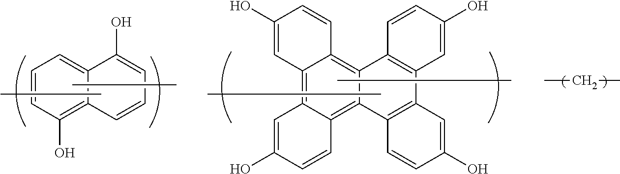 |
| Mw 4,320 Mw/Mn 2.72 | ||
| 8 | (A-8) |
 |
| Mw 3,640 Mw/Mn 2.32 | ||
| 9 | (A-9) |
 |
| Mw 3,210 Mw/Mn 2.53 | ||
| 10 | (A-10) |
 |
| 11 | (A-11) |
 |
| 12 | (A-12) |
 |
| Mw 4,210 Mw/Mn 2.86 | ||
| 13 | (A-13) |
 |
| Mw 3,210 Mw/Mn 2.72 | ||

(R-1): Mw=3,000 Mw/Mn=2.65

(R-2): Mw=4,000 Mw/Mn=3.21

(R-3): Mw=3,700 Mw/Mn=2.82
The compounds (A-1) to (A-13) and (R-1) to (R-3), a crosslinking agent (CR-1), an acid generator (AG-1), and an organic solvent were dissolved in a solvent containing 0.1 mass % FC-4430 (available from Sumitomo 3M Ltd.) with the proportion shown in Table 3. The solution was filtered through a 0.1-μm filter made of a fluorinated resin to prepare compositions for forming a resist underlayer film (UDL-1 to 23, Comparative UDL-1 to 3).
| TABLE 3 | |||||
| Composition for | Crosslinking | ||||
| forming resist | Compound | Compound | agent | Acid generator | Organic solvent |
| underlayer film | (part by mass) | (part by mass) | (part by mass) | (part by mass) | (part by mass) |
| UDL-1 | A-1 (10) | CR-1 (2) | AG-1 (0.5) | PGMEA (90) | |
| UDL-2 | A-2 (10) | CR-1 (2) | AG-1 (0.5) | PGMEA (90) | |
| UDL-3 | A-3 (10) | CR-1 (2) | AG-1 (0.5) | PGMEA (90) | |
| UDL-4 | A-4 (10) | AG-1 (0.5) | PGMEA (90) | ||
| UDL-5 | A-5 (10) | CR-1 (2) | AG-1 (0.5) | PGMEA (90) | |
| UDL-6 | A-6 (10) | AG-1 (0.5) | PGMEA (90) | ||
| UDL-7 | A-7 (10) | CR-1 (2) | AG-1 (0.5) | PGMEA (90) | |
| UDL-8 | A-8 (10) | CR-1 (2) | AG-1 (0.5) | PGMEA (90) | |
| UDL-9 | A-9 (10) | CR-1 (2) | AG-1 (0.5) | PGMEA (90) | |
| UDL-10 | A-10 (10) | AG-1 (0.5) | PGMEA (90) | ||
| UDL-11 | A-11 (10) | AG-1 (0.5) | PGMEA (90) | ||
| UDL-12 | A-12 (10) | CR-1 (2) | AG-1 (0.5) | PGMEA (90) | |
| UDL-13 | A-13 (10) | CR-1 (2) | AG-1 (0.5) | PGMEA (90) | |
| UDL-14 | A-1 (5) | A-10 (5) | AG-1 (0.5) | PGMEA (90) | |
| UDL-15 | A-2 (5) | A-4 (5) | AG-1 (0.5) | PGMEA (90) | |
| UDL-16 | A-10 (5) | R-1 (5) | AG-1 (0.5) | PGMEA (90) | |
| UDL-17 | A-2 (5) | R-2 (5) | PGMEA (90) | ||
| UDL-18 | A-11 (5) | R-3 (5) | PGMEA (90) | ||
| UDL-19 | A-1 (10) | PGMEA (90) | |||
| UDL-20 | A-5 (10) | PGMEA (90) | |||
| UDL-21 | A-7 (10) | PGMEA (90) | |||
| UDL-22 | A-12 (10) | PGMEA (90) | |||
| UDL-23 | A-13 (10) | PGMEA (90) | |||
| Comparative | R-1 (10) | CR-1 (2) | AG-1 (0.5) | PGMEA (90) | |
| UDL-1 | |||||
| Comparative | R-2 (10) | CR-1 (2) | AG-1 (0.5) | PGMEA (90) | |
| UDL-2 | |||||
| Comparative | R-3 (10) | CR-1 (2) | AG-1 (0.5) | PGMEA (90) | |
| UDL-3 | |||||
| PGMEA: propylene glycol monomethyl ether acetate | |||||
The acid generator (AG-1) and the crosslinking agent (CR-1) were shown below.

Compositions for forming a resist underlayer film prepared above (UDL-1 to 23 and comparative UDL-1 to 3) were each applied onto a silicon substrate and baked under a condition shown in Table 4 to form a coating film 200 nm thick. With respect to these film, optical properties (n-value and k-value) at 193 nm wavelength were measured by a spectroscopic ellipsometer with a variable incident light angle (VASE) manufactured by J. A. Woollam Co., Inc. The result is given in Table 4. Furthermore, nanoindentation test was conducted to measure hardness of the coating films by SA-2 nanoindenter instrument, manufactured by Toyo Corporation. The result is also given in Table 4.
| TABLE 4 | ||||
| Composition | ||||
| for forming | ||||
| resist | Optical properties | Hard- | ||
| underlayer | Firing | (193 nm) | ness | |
| film | temperature | n-value | k-value | (GPa) | |
| Example 1-1 | UDL-1 | 250° C., 60 sec | 1.48 | 0.41 | 0.80 |
| Example 1-2 | UDL-2 | 250° C., 60 sec | 1.47 | 0.38 | 0.76 |
| Example 1-3 | UDL-3 | 250° C., 60 sec | 1.47 | 0.45 | 0.78 |
| Example 1-4 | UDL-4 | 250° C., 60 sec | 1.43 | 0.46 | 0.69 |
| Example 1-5 | UDL-5 | 250° C., 60 sec | 1.58 | 0.26 | 0.64 |
| Example 1-6 | UDL-6 | 250° C., 60 sec | 1.47 | 0.26 | 0.62 |
| Example 1-7 | UDL-7 | 250° C., 60 sec | 1.48 | 0.40 | 0.68 |
| Example 1-8 | UDL-8 | 250° C., 60 sec | 1.49 | 0.48 | 0.66 |
| Example 1-9 | UDL-9 | 250° C., 60 sec | 1.48 | 0.44 | 0.75 |
| Example 1-10 | UDL-10 | 250° C., 60 sec | 1.44 | 0.45 | 0.80 |
| Example 1-11 | UDL-11 | 250° C., 60 sec | 1.43 | 0.45 | 0.80 |
| Example 1-12 | UDL-12 | 250° C., 60 sec | 1.39 | 0.40 | 0.68 |
| Example 1-13 | UDL-13 | 250° C., 60 sec | 1.41 | 0.43 | 0.66 |
| Example 1-14 | UDL-14 | 250° C., 60 sec | 1.46 | 0.43 | 0.82 |
| Example 1-15 | UDL-15 | 250° C., 60 sec | 1.46 | 0.40 | 0.67 |
| Example 1-16 | UDL-16 | 250° C., 60 sec | 1.45 | 0.39 | 0.65 |
| Example 1-17 | UDL-17 | 250° C., 60 sec | 1.48 | 0.49 | 0.63 |
| Example 1-18 | UDL-18 | 250° C., 60 sec | 1.43 | 0.41 | 0.70 |
| Example 1-19 | UDL-19 | 350° C., 60 sec | 1.43 | 0.46 | 0.82 |
| Example 1-20 | UDL-20 | 350° C., 60 sec | 1.53 | 0.29 | 0.70 |
| Example 1-21 | UDL-21 | 350° C., 60 sec | 1.43 | 0.45 | 0.74 |
| Example 1-22 | UDL-22 | 350° C., 60 sec | 1.34 | 0.44 | 0.66 |
| Example 1-23 | UDL-23 | 350° C., 60 sec | 1.36 | 0.48 | 0.67 |
| Comparative | Comparative | 250° C., 60 sec | 1.45 | 0.33 | 0.48 |
| Example 1-1 | UDL-1 | ||||
| Comparative | Comparative | 250° C., 60 sec | 1.49 | 0.61 | 0.52 |
| Example 1-2 | UDL-2 | ||||
| Comparative | Comparative | 250° C., 60 sec | 1.37 | 0.41 | 0.58 |
| Example 1-3 | UDL-3 | ||||
As shown in Table 4, the resist underlayer films in Examples 1-1 to 1-23 had a n-value (refractive index) of about 1.5 and a k-value (extinction coefficient) ranging from 0.25 to 0.49, and the optical properties meet the target value. Thus, these films are expected to exhibit a sufficient antireflective effect especially with a thickness of 200 nm or more, as the underlayer film for a three-layered resist.
Regarding hardness, the result of Examples 1-1 to 1-23 and Comparative Examples 1-1 to 1-3 indicates that the films using UDL-1 to 23 as the resist underlayer film composition had larger hardness, and thus were denser and stronger than the films using Comparative UDL-1 to 3. In particular, Examples 1-7, 1-8, and 1-12, which introduced the same repeating units as compounds (R-1) to (R-3) into the resin structure, and Examples 1-16 to 1-18, which combined compound (R-1) to (R-3), had larger hardness than Comparative Examples 1-1 to 1-3. This comparison emphasizes that introduction of the dibenzochrysene structure strengthened the film.
Compositions for forming a resist underlayer film (UDL-1 to 23 and comparative UDL-1 to 3) were each applied onto a 300-mm diameter Si wafer on which a SiO2 film 200 nm thick has been formed, and then baked at a firing temperature shown in Table 7 to form a resist underlayer film 200 nm thick. A silicon-containing resist middle layer film composition (SOG-1) was applied thereon and baked at 220° C. for 60 seconds to form a resist middle layer film 35 nm thick. A resist upper layer film composition (SL resist solution for ArF) was applied thereon and baked at 105° C. for 60 seconds to form a resist upper layer film 100 nm thick. Further, an immersion top coat composition (TC-1) was applied on the resist upper layer film and baked at 90° C. for 60 seconds to form a top coat 50 nm thick. The upper resist layer was prepared in the following manner: a polymer, an acid generator, and a basic compound were dissolved in a solvent containing 0.1 mass % FC-430 (available from Sumitomo 3M Ltd.) with the proportion shown in Table 5; and the solution was filtered through a 0.1-μm filter made of a fluorinated resin.
| TABLE 5 | ||||
| Basic | Solvent | |||
| Polymer | Acid generator | compound | (part | |
| No. | (part by mass) | (part by mass) | (part by mass) | by mass) |
| SL resist | ArF monolayer | PAG 1 (6.6) | Amine 1 (0.8) | PGMEA |
| for ArF | resist polymer 1 | (2500) | ||
| (100) | ||||

The silicon-containing resist middle layer film composition (SOG-1) used was prepared by dissolving the following polymer in a solvent.

The immersion top coat composition (TC-1) was prepared by dissolving the polymer in an organic solvent with the proportion shown in Table 6, followed by filtration through a 0.1-μm filter made of a fluorinated resin.
| TABLE 6 | |||
| Polymer | Organic solvent | ||
| (part by mass) | (part by mass) | ||
| TC-1 | Top coat polymer (100) | Diisoamyl ether (2700) | ||
| 2-Methyl-1-butanol (270) | ||||
Top Coat Polymer
Molecular weight (Mw)=8,800
Dispersity (Mw/Mn)=1.69

Subsequently, the wafer was exposed to light while the exposure dose is changed with an ArF liquid immersion exposure apparatus (NSR-S610C manufactured by Nikon Corporation, NA: 1.30, σ: 0.98/0.65, 35° s-polarized dipole illumination, 6% halftone phase shift mask), baked (PEB) at 100° C. for 60 seconds, and then developed with a 2.38 mass % tetramethylammonium hydroxide (TMAH) aqueous solution for 30 seconds to obtain a positive line-and-space pattern with a pitch of 100 nm and a resist line width ranging from 50 nm to 30 nm.
Then, the silicon-containing resist middle layer film was processed by dry etching using the resist pattern as a mask with an etching apparatus Telius, manufactured by Tokyo Electron Ltd. The resist underlayer film was then processed by using the obtained silicon-containing resist middle layer film pattern as a mask. The SiO2 film was then processed by using the obtained resist underlayer film pattern as a mask.
Etching conditions are as follows.
Transfer Condition of the Resist Pattern to the Silicon-Containing Resist Middle Layer Film:
| Chamber pressure | 10.0 | Pa | |
| RF power | 1,500 | W | |
| CF4 gas flow rate | 15 | sccm | |
| O2 gas flow rate | 75 | sccm | |
| Time | 15 | sec | |
Transfer Condition of the Silicon-Containing Resist Middle Layer Film Pattern to the Resist Underlayer Film:
| Chamber pressure | 2.0 | Pa | |
| RF power | 500 | W | |
| Ar gas flow rate | 75 | sccm | |
| O2 gas flow rate | 45 | sccm | |
| Time | 120 | sec | |
Transfer Condition of the Resist Underlayer Film Pattern to the SiO2 Film:
| Chamber pressure | 2.0 | Pa | |
| RF power | 2,200 | W | |
| C5F12 gas flow rate | 20 | sccm | |
| C2F6 |
10 | sccm | |
| Ar |
300 | sccm | |
| O2 gas flow rate | 60 | | |
| Time | |||
| 90 | sec | ||
Cross-section of the pattern was observed with an electron microscope (S-4700) manufactured by Hitachi, Ltd., and the shape was compared. The result is given in Table 7.
| TABLE 7 | ||||||||
| Minimum size | ||||||||
| Profile | (nm) without | |||||||
| Profile | after | pattern | ||||||
| Composition | after | etching for | Profile | wiggling | ||||
| for forming | Pattern | etching for | transferring | after | after | |||
| resist | profile | transferring | to | etching for | etching for | |||
| underlayer | Firing | after | to middle | underlayer | transferring | transferring | ||
| film | temperature | development | layer film | film | to substrate | to substrate | ||
| Example | UDL-1 | 250° C., | Vertical | Vertical | Vertical | Vertical | 25 |
| 2-1 | 60 sec | profile | profile | profile | profile | ||
| Example | UDL-2 | 250° C., | Vertical | Vertical | Vertical | Vertical | 26 |
| 2-2 | 60 sec | profile | profile | profile | profile | ||
| Example | UDL-3 | 250° C., | Vertical | Vertical | Vertical | Vertical | 26 |
| 2-3 | 60 sec | profile | profile | profile | profile | ||
| Example | UDL-4 | 250° C., | Vertical | Vertical | Vertical | Vertical | 29 |
| 2-4 | 60 sec | profile | profile | profile | profile | ||
| Example | UDL-5 | 250° C., | Vertical | Vertical | Vertical | Vertical | 31 |
| 2-5 | 60 sec | profile | profile | profile | profile | ||
| Example | UDL-6 | 250° C., | Vertical | Vertical | Vertical | Vertical | 32 |
| 2-6 | 60 sec | profile | profile | profile | profile | ||
| Example | UDL-7 | 250° C., | Vertical | Vertical | Vertical | Vertical | 29 |
| 2-7 | 60 sec | profile | profile | profile | profile | ||
| Example | UDL-8 | 250° C., | Vertical | Vertical | Vertical | Vertical | 30 |
| 2-8 | 60 sec | profile | profile | profile | profile | ||
| Example | UDL-9 | 250° C., | Vertical | Vertical | Vertical | Vertical | 27 |
| 2-9 | 60 sec | profile | profile | profile | profile | ||
| Example | UDL-10 | 250° C., | Vertical | Vertical | Vertical | Vertical | 25 |
| 2-10 | 60 sec | profile | profile | profile | profile | ||
| Example | UDL-11 | 250° C., | Vertical | Vertical | Vertical | Vertical | 25 |
| 2-11 | 60 sec | profile | profile | profile | profile | ||
| Example | UDL-12 | 250° C., | Vertical | Vertical | Vertical | Vertical | 29 |
| 2-12 | 60 sec | profile | profile | profile | profile | ||
| Example | UDL-13 | 250° C., | Vertical | Vertical | Vertical | Vertical | 30 |
| 2-13 | 60 sec | profile | profile | profile | profile | ||
| Example | UDL-14 | 250° C., | Vertical | Vertical | Vertical | Vertical | 24 |
| 2-14 | 60 sec | profile | profile | profile | profile | ||
| Example | UDL-15 | 250° C., | Vertical | Vertical | Vertical | Vertical | 30 |
| 2-15 | 60 sec | profile | profile | profile | profile | ||
| Example | UDL-16 | 250° C., | Vertical | Vertical | Vertical | Vertical | 31 |
| 2-16 | 60 sec | profile | profile | profile | profile | ||
| Example | UDL-17 | 250° C., | Vertical | Vertical | Vertical | Vertical | 32 |
| 2-17 | 60 sec | profile | profile | profile | profile | ||
| Example | UDL-18 | 250° C., | Vertical | Vertical | Vertical | Vertical | 29 |
| 2-18 | 60 sec | profile | profile | profile | profile | ||
| Example | UDL-19 | 350° C., | Vertical | Vertical | Vertical | Vertical | 25 |
| 2-19 | 60 sec | profile | profile | profile | profile | ||
| Example | UDL-20 | 350° C., | Vertical | Vertical | Vertical | Vertical | 29 |
| 2-20 | 60 sec | profile | profile | profile | profile | ||
| Example | UDL-21 | 350° C., | Vertical | Vertical | Vertical | Vertical | 27 |
| 2-21 | 60 sec | profile | profile | profile | profile | ||
| Example | UDL-22 | 350° C., | Vertical | Vertical | Vertical | Vertical | 30 |
| 2-22 | 60 sec | profile | profile | profile | profile | ||
| Example | UDL-23 | 350° C., | Vertical | Vertical | Vertical | Vertical | 20 |
| 2-23 | 60 sec | profile | profile | profile | profile | ||
| Comparative | Comparative | 250° C., | Vertical | Vertical | Vertical | Vertical | 42 |
| Example 2-1 | UDL-1 | 60 sec | profile | profile | profile | profile | |
| Comparative | Comparative | 250° C., | Uneven | — | — | — | — |
| Example 2-2 | UDL-2 | 60 sec | profile | ||||
| Comparative | Comparative | 250° C., | Vertical | Vertical | Vertical | Vertical | 38 |
| Example 2-3 | UDL-3 | 60 sec | profile | profile | profile | profile | |
The resist underlayer films formed by using UDL-1 to 23, which are the inventive composition for forming a resist underlayer film, had n-value and k-value suited to practical use as the underlayer film of the three-layered resist for liquid immersion lithography, as shown in Table 4. Thus, these films had a good resist shape after development in the pattern evaluation shown in Table 7. By contrast, Comparative Example 2-2 (Comparative UDL-2) resulted in a poor resist shape, so that etching evaluation was impossible. This poor shape is supposed to be caused by insufficient antireflective effect because the combination of n-value and k-value of Comparative UDL-2 was out of the optimum values.
In addition, as shown in Table 7, when UDL-1 to 23, which are the inventive composition for forming a resist underlayer film, were used, the resist shape after development and the resist underlayer film shape after etching with oxygen and after etching for processing the substrate were good. The pattern size after substrate transfer changed in accordance with the resist line width formed by the photo-exposure. While Comparative UDL-1 and UDL-3 caused pattern wiggling at a line width of about 40 nm, UDL-1 to 23, which are the inventive composition for forming a resist underlayer film, did not cause wiggling until a pattern size of 35 nm or less, so that a high wiggling resistance could be confirmed.
This indicates that high wiggling resistance can be achieved by using a dense resist underlayer film having a hardness of more than 0.60 GPa, like the resist underlayer film formed by using the inventive composition for forming a resist underlayer film.
As described above, the resist underlayer film obtained from the inventive composition for forming a resist underlayer film has suitable optical properties for providing a sufficient antireflective effect and excellent wiggling resistance during etching, and thus is very useful as the underlayer film for a multilayer resist process, especially three-layer resist process, for ultra-fine patterning with high precision.
It is to be noted that the present invention is not restricted to the foregoing embodiment. The embodiment is just an exemplification, and any examples that have substantially the same feature and demonstrate the same functions and effects as those in the technical concept described in claims of the present invention are included in the technical scope of the present invention.
Claims (20)
1. A composition for forming a resist underlayer film, comprising an organic solvent and either or both of a compound shown by the following general formula (1) and a condensate of the compound,

wherein R1, R3, R5, and R7 represent Z1, a diglycidylamino group, or a dipropargylamino group; R2, R4, R6, and R8 represent Z2, a glycidyl group, a diglycidylamino group, or a dipropargylamino group; X represents a group shown by the following formula (1-1); n1 to n8 are each a number satisfying 0≦n1≦4, 0≦n2≦4, 0≦n3≦4, 0≦n4≦4, 0≦n5≦4, 0≦n6≦4, 0≦n7≦4, 0≦n8≦4, 0≦n1+n2≦4, 0≦n3+n4≦4, 0≦n5+n6≦4, 0≦n7+n8≦4, and 1≦n1+n2+n3+n4+n5+n6+n7+n8≦16, where Z1 represents an alkyl group having 1 to 20 carbon atoms, an alkenyl group or alkynyl group having 2 to 20 carbon atoms, or an aryl group having 6 to 30 carbon atoms, and Z2 represents Z1, a hydrogen atom, or a hydroxyaryl group having 6 to 14 carbon atoms,

wherein * represents a binding site with Rp where p represents 2, 4, 6, or 8.
2. The composition for forming a resist underlayer film according to claim 1 , wherein the condensate is obtained by a reaction of one or more compounds shown by the general formula (1) with one or more compounds selected from a compound shown by the following general formula (2-1), a compound shown by the following general formula (2-2), trioxane, paraformaldehyde, and fluorenone,
Y1—CHO (2-1)
Y1—CHO (2-1)
wherein Y1 represents a hydrogen atom or a monovalent organic group having 1 to 30 carbon atoms and optionally containing a substituent,
R9—CH2—Y2—CH2—R9 (2-2)
R9—CH2—Y2—CH2—R9 (2-2)
wherein Y2 represents an aromatic group having 6 or more carbon atoms and optionally containing a substituent; R9 represents an alkoxy group or alkanoyloxy group having 1 to 6 carbon atoms, or a halogen atom.
3. The composition for forming a resist underlayer film according to claim 1 , wherein the condensate is obtained by a reaction with one or more compounds selected from compounds shown by the following general formulae (3-1), (3-2), (3-3), (3-4), and (3-5),

wherein R11 and R13 represent Z1, where Z1 is as defined above, an amino group, a diglycidylamino group, or a dipropargylamino group; R12 and R14 represent Z2, where Z2 is as defined above, a glycidyl group, a diglycidylamino group, or a dipropargylamino group; a single bond contained in R11 to R14 may be substituted by a double bond, a triple bond, an ether group, a carbonyl group, or a carbonyloxy group; a hydrogen atom contained in R11 to R14 may be substituted by a fluorine atom, a chlorine atom, or a hydroxyl group; two substituents selected from R11, R12, R13, and R14 may be bonded intramolecularly to form a cyclic substituent; X1 represents a group shown by the following formula (3-6); and n11 to n14 are each a number satisfying 0≦n11≦4, 0≦n12≦4, 0≦n13≦4, 0≦n14≦4, 0≦n11+n12≦4, 0≦n13+n14≦4, and 1≦n11+n12+n13+n14≦8,

wherein R15 represents a fluorine atom, a chlorine atom, Z1, where Z1 is as defined above, a diglycidylamino group, or a dipropargylamino group; R16 represents Z2, where Z2 is as defined above, a glycidyl group, a diglycidylamino group, or a dipropargylamino group; a single bond contained in R15 and R16 may be substituted by a double bond, a triple bond, an ether group, a carbonyl group, or a carbonyloxy group; a hydrogen atom contained in R15 and R16 may be substituted by a fluorine atom, a chlorine atom, or a hydroxyl group; two substituents selected from R15 and R16 may be bonded intramolecularly to form a cyclic substituent; X1 represents a group shown by the following formula (3-6); and n15 and n16 are each a number satisfying 0≦n15≦6, 0≦n16≦6, and 1≦n15+n16≦6,

wherein R17, R19, R21, and R23 represent Z1, where Z1 is as defined above, a diglycidylamino group, or a dipropargylamino group; R18 and R22 represent Z2, where Z2 is as defined above, a glycidyl group, a glycidyloxyethyl group, a diglycidylamino group, or a dipropargylamino group; R20 and R24 represent Z2, where Z2 is as defined above, a glycidyl group, a diglycidylamino group, or a dipropargylamino group; a single bond contained in R17 to R24 may be substituted by a double bond, a triple bond, an ether group, a carbonyl group, or a carbonyloxy group; a hydrogen atom contained in R17 to R24 may be substituted by a fluorine atom, a chlorine atom, or a hydroxyl group; X1 represents a group shown by the following formula (3-6); and n17 to n24 are each a number satisfying 0≦n17≦4, 0≦n18≦4, 0≦n19≦3, 0≦n20≦3, 0≦n21≦4, 0≦n22≦4, 0≦n23≦3, 0≦n24≦3, 0≦n17+n18≦4, 0≦n19+n20≦3, 0≦n21+n22≦4, 0≦n23+n24≦3, 1≦n17+n18+n19+n20≦7, and 1≦n21+n22+n23+n24≦7,

wherein R25 and R27 represent Z1, where Z1 is as defined above, a diglycidylamino group, or a dipropargylamino group; R26 and R28 represent Z2, where Z2 is as defined above, a glycidyl group, a glycidyloxyethyl group, a diglycidylamino group, or a dipropargylamino group; a single bond contained in R25 to R28 may be substituted by a double bond, a triple bond, an ether group, a carbonyl group, or a carbonyloxy group; a hydrogen atom contained in R25 to R28 may be substituted by a fluorine atom, a chlorine atom, or a hydroxyl group; X1 represents a group shown by the following formula (3-6); and n25 to n28 are each a number satisfying 0≦n25≦5, 0≦n26≦5, 0≦n27≦5, 0≦n28≦5, 1≦n25+n26≦5, and 1≦n27+n28≦5,

wherein R29 and R31 represent Z1, where Z1 is as defined above, a diglycidylamino group, or a dipropargylamino group; R30, R32, and R33 represent Z2, where Z2 is as defined above, a glycidyl group, a diglycidylamino group, or a dipropargylamino group; a single bond contained in R29 to R33 may be substituted by a double bond, a triple bond, an ether group, a carbonyl group, or a carbonyloxy group; a hydrogen atom contained in R29 to R33 may be substituted by a fluorine atom, a chlorine atom, or a hydroxyl group; X1 represents a group shown by the following formula (3-6); and n29 to n32 are each a number satisfying 0≦n29≦4, 0≦n30≦4, 0≦n31≦4, 0≦n32≦4, 0≦n29+n30≦4, and 0≦n31+n32≦4,

wherein * represents a binding site with Rq where q represents 12, 14, 16, 18, 20, 22, 24, 26, 28, 30, or 32.
4. The composition for forming a resist underlayer film according to claim 2 , wherein the condensate is obtained by a reaction with one or more compounds selected from compounds shown by the following general formulae (3-1), (3-2), (3-3), (3-4), and (3-5),
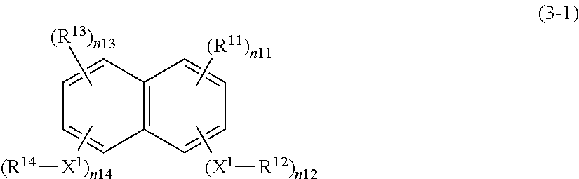
wherein R11 and R13 represent Z1, where Z1 is as defined above, an amino group, a diglycidylamino group, or a dipropargylamino group; R12 and R14 represent Z2, where Z2 is as defined above, a glycidyl group, a diglycidylamino group, or a dipropargylamino group; a single bond contained in R11 to R14 may be substituted by a double bond, a triple bond, an ether group, a carbonyl group, or a carbonyloxy group; a hydrogen atom contained in R1 to R14 may be substituted by a fluorine atom, a chlorine atom, or a hydroxyl group; two substituents selected from R11, R12, R13, and R14 may be bonded intramolecularly to form a cyclic substituent; X1 represents a group shown by the following formula (3-6); and n11 to n14 are each a number satisfying 0≦n1≦4, 0≦n12≦4, 0≦n13≦4, 0≦n14≦4, 0≦n11+n12≦4, 0≦n13+n14≦4, and 1≦n11+n12+n13+n14≦8,

wherein R15 represents a fluorine atom, a chlorine atom, Z1, where Z1 is as defined above, a diglycidylamino group, or a dipropargylamino group; R16 represents Z2, where Z2 is as defined above, a glycidyl group, a diglycidylamino group, or a dipropargylamino group; a single bond contained in R15 and R16 may be substituted by a double bond, a triple bond, an ether group, a carbonyl group, or a carbonyloxy group; a hydrogen atom contained in R15 and R16 may be substituted by a fluorine atom, a chlorine atom, or a hydroxyl group; two substituents selected from R15 and R16 may be bonded intramolecularly to form a cyclic substituent; X1 represents a group shown by the following formula (3-6); and n15 and n16 are each a number satisfying 0≦n15≦6, 0≦n16≦6, and 1≦n15+n16≦6,

wherein R17, R19, R21, and R23 represent Z1, where Z1 is as defined above, a diglycidylamino group, or a dipropargylamino group; R18 and R22 represent Z2, where Z2 is as defined above, a glycidyl group, a glycidyloxyethyl group, a diglycidylamino group, or a dipropargylamino group; R20 and R24 represent Z2, where Z2 is as defined above, a glycidyl group, a diglycidylamino group, or a dipropargylamino group; a single bond contained in R17 to R24 may be substituted by a double bond, a triple bond, an ether group, a carbonyl group, or a carbonyloxy group; a hydrogen atom contained in R17 to R24 may be substituted by a fluorine atom, a chlorine atom, or a hydroxyl group; X1 represents a group shown by the following formula (3-6); and n17 to n24 are each a number satisfying 0≦n17≦4, 0≦n18≦4, 0≦n19≦3, 0≦n20≦3, 0≦n21≦4, 0≦n22≦4, 0≦n23≦3, 0≦n24≦3, 0≦n17+n18≦4, 0≦n19+n20≦3, 0≦n21+n22≦4, 0≦n23+n24≦3, 1≦n17+n18+n19+n20≦7, and 1≦n21+n22+n23+n24≦7,

wherein R25 and R27 represent Z1, where Z1 is as defined above, a diglycidylamino group, or a dipropargylamino group; R26 and R28 represent Z2, where Z2 is as defined above, a glycidyl group, a glycidyloxyethyl group, a diglycidylamino group, or a dipropargylamino group; a single bond contained in R25 to R28 may be substituted by a double bond, a triple bond, an ether group, a carbonyl group, or a carbonyloxy group; a hydrogen atom contained in R25 to R28 may be substituted by a fluorine atom, a chlorine atom, or a hydroxyl group; X1 represents a group shown by the following formula (3-6); and n25 to n28 are each a number satisfying 0≦n25≦5, 0≦n26≦5, 0≦n27≦5, 0≦n28≦5, 1≦n25+n26≦5, and 1≦n27+n28≦5,

wherein R29 and R31 represent Z1, where Z1 is as defined above, a diglycidylamino group, or a dipropargylamino group; R39, R32, and R33 represent Z2, where Z2 is as defined above, a glycidyl group, a diglycidylamino group, or a dipropargylamino group; a single bond contained in R29 to R33 may be substituted by a double bond, a triple bond, an ether group, a carbonyl group, or a carbonyloxy group; a hydrogen atom contained in R29 to R33 may be substituted by a fluorine atom, a chlorine atom, or a hydroxyl group; X1 represents a group shown by the following formula (3-6); and n29 to n32 are each a number satisfying 0≦n29≦4, 0≦n30≦4, 0≦n31≦4, 0≦n32≦4, 0≦n29+n30≦4, and 0≦n31+n32≦4,

wherein * represents a binding site with R4 where q represents 12, 14, 16, 18, 20, 22, 24, 26, 28, 30, or 32.
5. The composition for forming a resist underlayer film according to claim 1 , further comprising a substituted condensate obtained by substituting a part of hydrogen atoms contained in the condensate by a glycidyl group.
6. The composition for forming a resist underlayer film according to claim 2 , further comprising a substituted condensate obtained by substituting a part of hydrogen atoms contained in the condensate by a glycidyl group.
7. The composition for forming a resist underlayer film according to claim 3 , further comprising a substituted condensate obtained by substituting a part of hydrogen atoms contained in the condensate by a glycidyl group.
8. The composition for forming a resist underlayer film according to claim 4 , further comprising a substituted condensate obtained by substituting a part of hydrogen atoms contained in the condensate by a glycidyl group.
9. The composition for forming a resist underlayer film according to claim 1 , wherein the composition for forming a resist underlayer film comprises two or more of the compound shown by the general formula (1), the condensate of the compound, and a substituted condensate obtained by substituting a part of hydrogen atoms of the condensate by a glycidyl group.
10. The composition for forming a resist underlayer film according to claim 2 , wherein the composition for forming a resist underlayer film comprises two or more of the compound shown by the general formula (1), the condensate of the compound, and a substituted condensate obtained by substituting a part of hydrogen atoms of the condensate by a glycidyl group.
11. The composition for forming a resist underlayer film according to claim 1 , further comprising either or both of a crosslinking agent and an acid generator.
12. A patterning process comprising: forming a resist underlayer film on a body to be processed by using the composition for forming a resist underlayer film according to claim 1 ; forming a resist middle layer film on the resist underlayer film by using a silicon-containing resist middle layer film composition; forming a resist upper layer film on the resist middle layer film by using a resist upper layer film composition which is a photoresist composition; forming a circuit pattern on the resist upper layer film; etching the resist middle layer film by using the resist upper layer film having the formed pattern as a mask; etching the resist underlayer film by using the resist middle layer film having the formed pattern as a mask; further etching the body to be processed by using the resist underlayer film having the formed pattern as a mask, whereby the pattern is formed in the body to be processed.
13. A patterning process comprising: forming a resist underlayer film on a body to be processed by using the composition for forming a resist underlayer film according to claim 1 ; forming a resist middle layer film on the resist underlayer film by using a silicon-containing resist middle layer film composition; forming an organic antireflective film (BARC) on the resist middle layer film; forming a resist upper layer film on the BARC by using a resist upper layer film composition which is a photoresist composition and thereby forming a 4-layered resist film; forming a circuit pattern on the resist upper layer film; etching the BARC film and the resist middle layer film by using the resist upper layer film having the formed pattern as a mask; etching the resist underlayer film by using the resist middle layer film having the formed pattern as a mask; further etching the body to be processed by using the resist underlayer film having the formed pattern as a mask, whereby the pattern is formed in the body to be processed.
14. A patterning process comprising: forming a resist underlayer film on a body to be processed by using the composition for forming a resist underlayer film according to claim 1 ; forming an inorganic hard mask intermediate film selected from a silicon oxide film, a silicon nitride film, and a silicon oxynitride film on the resist underlayer film; forming a resist upper layer film on the inorganic hard mask intermediate film by using a resist upper layer film composition which is a photoresist composition; forming a circuit pattern on the resist upper layer film; etching the inorganic hard mask intermediate film by using the resist upper layer film having the formed pattern as a mask; etching the resist underlayer film by using the inorganic hard mask intermediate film having the formed pattern as a mask; further etching the body to be processed by using the resist underlayer film having the formed pattern as a mask, whereby the pattern is formed in the body to be processed.
15. A patterning process comprising: forming a resist underlayer film on a body to be processed by using the composition for forming a resist underlayer film according to claim 1 ; forming an inorganic hard mask intermediate film selected from a silicon oxide film, a silicon nitride film, and a silicon oxynitride film on the resist underlayer film; forming an organic antireflective film (BARC) on the inorganic hard mask intermediate film; forming a resist upper layer film on the BARC by using a resist upper layer film composition which is a photoresist composition and thereby forming a 4-layered resist film; forming a circuit pattern on the resist upper layer film; etching the BARC film and the inorganic hard mask intermediate film by using the resist upper layer film having the formed pattern as a mask; etching the resist underlayer film by using the inorganic hard mask intermediate film having the formed pattern as a mask; further etching the body to be processed by using the resist underlayer film having the formed pattern as a mask, whereby the pattern is formed in the body to be processed.
16. The patterning process according to claim 14 , wherein the inorganic hard mask intermediate film is formed by a CVD method or an ALD method.
17. The patterning process according to claim 12 , wherein the resist upper layer film is patterned by a photolithography with a wavelength ranging from 10 nm to 300 nm, a direct drawing by electron beam, a nanoimprinting, or a combination thereof.
18. The patterning process according to claim 12 , wherein a development method in the patterning process is an alkaline development or a development with an organic solvent.
19. The patterning process according to claim 12 , wherein the body to be processed is a semiconductor apparatus substrate or the semiconductor apparatus substrate coated with any of a metal film, a metal carbide film, a metal oxide film, a metal nitride film, a metal oxycarbide film, and a metal oxynitride film.
20. The patterning process according to claim 19 , wherein the metal is silicon, titanium, tungsten, hafnium, zirconium, chromium, germanium, copper, silver, gold, aluminum, indium, gallium, arsenic, palladium, iron, tantalum, iridium, molybdenum, or an alloy thereof.
Applications Claiming Priority (2)
| Application Number | Priority Date | Filing Date | Title |
|---|---|---|---|
| JP2015-139659 | 2015-07-13 | ||
| JP2015139659 | 2015-07-13 |
Publications (2)
| Publication Number | Publication Date |
|---|---|
| US20170017156A1 US20170017156A1 (en) | 2017-01-19 |
| US9857686B2 true US9857686B2 (en) | 2018-01-02 |
Family
ID=57775771
Family Applications (1)
| Application Number | Title | Priority Date | Filing Date |
|---|---|---|---|
| US15/178,982 Active US9857686B2 (en) | 2015-07-13 | 2016-06-10 | Composition for forming resist underlayer film and patterning process |
Country Status (4)
| Country | Link |
|---|---|
| US (1) | US9857686B2 (en) |
| JP (1) | JP6712188B2 (en) |
| KR (1) | KR102004027B1 (en) |
| TW (1) | TWI620028B (en) |
Cited By (2)
| Publication number | Priority date | Publication date | Assignee | Title |
|---|---|---|---|---|
| US10189947B2 (en) * | 2016-01-11 | 2019-01-29 | Sang Jun Choi | Composition of anti-reflective hardmask |
| US20190041753A1 (en) * | 2017-08-04 | 2019-02-07 | Shin-Etsu Chemical Co., Ltd. | Resist multilayer film-attached substrate and patterning process |
Families Citing this family (26)
| Publication number | Priority date | Publication date | Assignee | Title |
|---|---|---|---|---|
| JP6711104B2 (en) * | 2015-04-24 | 2020-06-17 | Jsr株式会社 | Resist underlayer film forming method and pattern forming method |
| JP6714492B2 (en) * | 2015-12-24 | 2020-06-24 | 信越化学工業株式会社 | Organic film forming compound, organic film forming composition, organic film forming method, and pattern forming method |
| JP6714493B2 (en) | 2015-12-24 | 2020-06-24 | 信越化学工業株式会社 | Organic film forming compound, organic film forming composition, organic film forming method, and pattern forming method |
| JP6977272B2 (en) | 2017-02-08 | 2021-12-08 | 凸版印刷株式会社 | Exterior materials for power storage devices and power storage devices |
| KR101775586B1 (en) * | 2017-02-15 | 2017-09-11 | 동우 화인켐 주식회사 | Composition for hard mask |
| KR102349937B1 (en) * | 2017-03-27 | 2022-01-10 | 동우 화인켐 주식회사 | Composition for hard mask |
| JP6853716B2 (en) | 2017-03-31 | 2021-03-31 | 信越化学工業株式会社 | Resist underlayer film material, pattern forming method, and resist underlayer film forming method |
| TWI748087B (en) * | 2017-04-25 | 2021-12-01 | 日商日產化學工業股份有限公司 | Resistor underlayer film forming composition using stilbene compound |
| JP6726142B2 (en) * | 2017-08-28 | 2020-07-22 | 信越化学工業株式会社 | Organic film forming composition, semiconductor device manufacturing substrate, organic film forming method, pattern forming method, and polymer |
| JP6940335B2 (en) * | 2017-08-30 | 2021-09-29 | 信越化学工業株式会社 | Organic film forming composition, semiconductor device manufacturing substrate, organic film forming method, pattern forming method, and polymer |
| JP6894364B2 (en) * | 2017-12-26 | 2021-06-30 | 信越化学工業株式会社 | Organic film forming composition, semiconductor device manufacturing substrate, organic film forming method, and pattern forming method |
| CN109988325B (en) * | 2018-01-03 | 2021-01-26 | 中国科学院化学研究所 | Large-area ultrathin high-crystalline-state two-dimensional conjugated polymer film and preparation method and application thereof |
| US11248086B2 (en) * | 2018-05-01 | 2022-02-15 | Tokyo Ohka Kogyo Co., Ltd. | Hard-mask forming composition and method for manufacturing electronic component |
| US11650503B2 (en) * | 2018-08-02 | 2023-05-16 | Tokyo Ohka Kogyo Co., Ltd. | Hard mask-forming composition and method for manufacturing electronic component |
| WO2020169702A1 (en) * | 2019-02-22 | 2020-08-27 | Merck Patent Gmbh | Spin-on compositions comprising an inorganic oxide component and an alkynyloxy substituted spin-on carbon component useful as hard masks and filling materials with improved shelf life |
| CN110041286B (en) * | 2019-05-10 | 2021-03-19 | 福建泓光半导体材料有限公司 | Hard mask monomer, composition and pattern forming method |
| US20200379347A1 (en) * | 2019-05-31 | 2020-12-03 | Rohm And Haas Electronic Materials Llc | Resist underlayer compositions and pattern formation methods using such compositions |
| JP7375347B2 (en) * | 2019-06-28 | 2023-11-08 | Dic株式会社 | Epoxy compounds, compositions, cured products and laminates |
| JP2021008411A (en) * | 2019-06-28 | 2021-01-28 | Dic株式会社 | Hydroxy compound, composition, cured product and laminate |
| CN112768342B (en) * | 2019-11-02 | 2022-03-22 | 长鑫存储技术有限公司 | Semiconductor structure and forming method thereof |
| WO2021112194A1 (en) * | 2019-12-04 | 2021-06-10 | 三菱瓦斯化学株式会社 | Composition for forming underlayer film for lithography, underlayer film for lithography, resist pattern forming method, circuit pattern forming method, oligomer, and purification method |
| CN111341497B (en) * | 2020-03-13 | 2021-06-08 | 浙江大学 | Preparation method of silver nanowire-MXene composite transparent conductive film |
| US20220066321A1 (en) * | 2020-08-31 | 2022-03-03 | Rohm And Haas Electronic Materials Llc | Underlayer compositions and patterning methods |
| US11762294B2 (en) * | 2020-08-31 | 2023-09-19 | Rohm And Haas Electronic Materials Llc | Coating composition for photoresist underlayer |
| KR20240025531A (en) * | 2021-06-24 | 2024-02-27 | 제이에스알 가부시끼가이샤 | Method and composition for manufacturing semiconductor substrates |
| KR102396715B1 (en) * | 2021-10-21 | 2022-05-13 | 이근수 | Process of preparing hardmask film including metal and forming resist pattern |
Citations (29)
| Publication number | Priority date | Publication date | Assignee | Title |
|---|---|---|---|---|
| US4829090A (en) * | 1983-05-17 | 1989-05-09 | Burroughs Wellcome Co. | Chrysene derivatives |
| JPH06118651A (en) | 1992-10-08 | 1994-04-28 | Nippon Telegr & Teleph Corp <Ntt> | Positive type resist material |
| US5494944A (en) * | 1984-02-10 | 1996-02-27 | Ciba-Geigy Corporation | Hardenable composition and its use |
| US20040191479A1 (en) | 2003-03-24 | 2004-09-30 | Shin-Etsu Chemical Co., Ltd. | Anti-reflection film material and a substrate having an anti-reflection film and a method for forming a pattern |
| US20060019195A1 (en) | 2003-10-03 | 2006-01-26 | Jun Hatakeyama | Photoresist undercoat-forming material and patterning process |
| JP2007199653A (en) | 2005-12-27 | 2007-08-09 | Shin Etsu Chem Co Ltd | Photoresist underlayer film forming material and pattern forming method |
| US20070238300A1 (en) | 2006-04-11 | 2007-10-11 | Shin-Etsu Chemical Co., Ltd. | Silicon-containing film-forming composition, silicon-containing film, silicon-containing film-bearing substrate, and patterning method |
| JP2007302873A (en) | 2006-04-11 | 2007-11-22 | Shin Etsu Chem Co Ltd | Silicon-containing film-forming composition, silicon-containing film, silicon-containing film-bearing substrate, and patterning method using the same substrate |
| JP2008111103A (en) | 2006-10-04 | 2008-05-15 | Shin Etsu Chem Co Ltd | Polymer compound, resist material, and pattern-forming method |
| US20080118860A1 (en) | 2006-10-04 | 2008-05-22 | Shin-Etsu Chemical Co., Ltd. | Polymer, resist composition, and patterning process |
| US20090136869A1 (en) | 2007-11-22 | 2009-05-28 | Tsutomu Ogihara | Metal oxide-containing film-forming composition, metal oxide-containing film, metal oxide-containing film-bearing substrate, and patterning method |
| JP4355943B2 (en) | 2003-10-03 | 2009-11-04 | 信越化学工業株式会社 | Photoresist underlayer film forming material and pattern forming method |
| US20120108071A1 (en) | 2010-11-01 | 2012-05-03 | Shin-Etsu Chemical Co., Ltd. | Resist underlayer film composition and patterning process using the same |
| US20120142193A1 (en) | 2010-12-01 | 2012-06-07 | Shin-Etsu Chemical Co., Ltd. | Resist underlayer film composition and patterning process using the same |
| US20120153511A1 (en) * | 2010-12-16 | 2012-06-21 | Jee-Yun Song | Hardmask composition and method of forming patterns and semiconductor integrated circuit device including the patterns |
| US20120184103A1 (en) | 2011-01-14 | 2012-07-19 | Shin-Etsu Chemical Co., Ltd. | Resist underlayer film composition and patterning process using the same |
| US20120270994A1 (en) * | 2009-12-31 | 2012-10-25 | Min-Soo Kim | Aromatic ring-containing polymer for underlayer of resist and resist underlayer composition including the same |
| US20120308832A1 (en) * | 2010-02-03 | 2012-12-06 | Dic Corporation | Phenol resin composition, production method therefor, curable resin composition, cured product thereof, and printed circuit board |
| US20130171569A1 (en) * | 2012-01-04 | 2013-07-04 | Shin-Etsu Chemical Co., Ltd. | Resist underlayer film composition, method for producing polymer for resist underlayer film, and patterning process using the resist underlayer film composition |
| US20130189533A1 (en) * | 2010-10-14 | 2013-07-25 | Nissan Chemical Industries, Ltd. | Resist underlayer film forming composition for lithography containing polyether structure-containing resin |
| JP2013227307A (en) * | 2012-03-29 | 2013-11-07 | Kurogane Kasei Co Ltd | New compound and polymer using the same |
| US8993215B2 (en) * | 2012-03-27 | 2015-03-31 | Nissan Chemical Industries, Ltd. | Resist underlayer film forming composition containing phenylindole-containing novolac resin |
| US9116429B2 (en) * | 2009-11-13 | 2015-08-25 | Cheil Industries, Inc. | Resist underlayer polymer, resist underlayer composition including the same, and method of patterning using the same |
| US20160017174A1 (en) * | 2014-07-15 | 2016-01-21 | Samsung Sdi Co., Ltd. | Hardmask composition and method of forming patterns using the hardmask composition |
| US9263285B2 (en) * | 2010-12-09 | 2016-02-16 | Nissan Chemical Industries, Ltd. | Composition for forming a resist underlayer film including hydroxyl group-containing carbazole novolac resin |
| US9334357B2 (en) * | 2014-04-30 | 2016-05-10 | Rohm And Haas Electronic Materials Llc | Aromatic resins for underlayers |
| US20160257842A1 (en) * | 2015-03-03 | 2016-09-08 | Jsr Corporation | Composition for resist underlayer film formation, resist underlayer film, and production method of patterned substrate |
| US9469777B2 (en) * | 2012-08-21 | 2016-10-18 | Nissan Chemical Industries, Ltd. | Resist underlayer film forming composition that contains novolac resin having polynuclear phenol |
| US9556094B2 (en) * | 2012-12-26 | 2017-01-31 | Cheil Industries, Inc. | Monomer, hardmask composition including monomer, and method for forming pattern by using hardmask composition |
Family Cites Families (5)
| Publication number | Priority date | Publication date | Assignee | Title |
|---|---|---|---|---|
| JP4826805B2 (en) * | 2006-08-30 | 2011-11-30 | 信越化学工業株式会社 | Photoresist underlayer film material, photoresist underlayer film substrate, and pattern forming method |
| JP5177137B2 (en) * | 2007-05-23 | 2013-04-03 | Jsr株式会社 | Composition for forming a resist underlayer film |
| KR20150079199A (en) * | 2013-12-31 | 2015-07-08 | 제일모직주식회사 | Hardmask composition, method of forming patterns using the hardmask composition and semiconductor integrated circuit device including the patterns |
| KR101667788B1 (en) * | 2013-12-31 | 2016-10-19 | 제일모직 주식회사 | Hardmask composition, and method of forming patterns using the hardmask composition |
| JP6447884B2 (en) * | 2014-05-08 | 2019-01-09 | 三菱瓦斯化学株式会社 | Lithographic film forming material, Lithographic film forming composition, Lithographic film, pattern forming method and purification method |
-
2016
- 2016-05-26 JP JP2016105420A patent/JP6712188B2/en active Active
- 2016-06-10 US US15/178,982 patent/US9857686B2/en active Active
- 2016-07-12 KR KR1020160088102A patent/KR102004027B1/en active IP Right Grant
- 2016-07-12 TW TW105121837A patent/TWI620028B/en active
Patent Citations (34)
| Publication number | Priority date | Publication date | Assignee | Title |
|---|---|---|---|---|
| US4829090A (en) * | 1983-05-17 | 1989-05-09 | Burroughs Wellcome Co. | Chrysene derivatives |
| US5494944A (en) * | 1984-02-10 | 1996-02-27 | Ciba-Geigy Corporation | Hardenable composition and its use |
| JPH06118651A (en) | 1992-10-08 | 1994-04-28 | Nippon Telegr & Teleph Corp <Ntt> | Positive type resist material |
| US20040191479A1 (en) | 2003-03-24 | 2004-09-30 | Shin-Etsu Chemical Co., Ltd. | Anti-reflection film material and a substrate having an anti-reflection film and a method for forming a pattern |
| JP2004310019A (en) | 2003-03-24 | 2004-11-04 | Shin Etsu Chem Co Ltd | Antireflection film material, substrate having antireflection film and method for forming pattern |
| JP4355943B2 (en) | 2003-10-03 | 2009-11-04 | 信越化学工業株式会社 | Photoresist underlayer film forming material and pattern forming method |
| US20060019195A1 (en) | 2003-10-03 | 2006-01-26 | Jun Hatakeyama | Photoresist undercoat-forming material and patterning process |
| JP2007199653A (en) | 2005-12-27 | 2007-08-09 | Shin Etsu Chem Co Ltd | Photoresist underlayer film forming material and pattern forming method |
| JP2007302873A (en) | 2006-04-11 | 2007-11-22 | Shin Etsu Chem Co Ltd | Silicon-containing film-forming composition, silicon-containing film, silicon-containing film-bearing substrate, and patterning method using the same substrate |
| US20070238300A1 (en) | 2006-04-11 | 2007-10-11 | Shin-Etsu Chemical Co., Ltd. | Silicon-containing film-forming composition, silicon-containing film, silicon-containing film-bearing substrate, and patterning method |
| JP2008111103A (en) | 2006-10-04 | 2008-05-15 | Shin Etsu Chem Co Ltd | Polymer compound, resist material, and pattern-forming method |
| US20080118860A1 (en) | 2006-10-04 | 2008-05-22 | Shin-Etsu Chemical Co., Ltd. | Polymer, resist composition, and patterning process |
| US20090136869A1 (en) | 2007-11-22 | 2009-05-28 | Tsutomu Ogihara | Metal oxide-containing film-forming composition, metal oxide-containing film, metal oxide-containing film-bearing substrate, and patterning method |
| JP2009126940A (en) | 2007-11-22 | 2009-06-11 | Shin Etsu Chem Co Ltd | Composition for forming metal oxide-containing film, metal oxide-containing film, substrate having metal oxide-containing film formed thereon, and pattern formation method using the same |
| US9116429B2 (en) * | 2009-11-13 | 2015-08-25 | Cheil Industries, Inc. | Resist underlayer polymer, resist underlayer composition including the same, and method of patterning using the same |
| US20120270994A1 (en) * | 2009-12-31 | 2012-10-25 | Min-Soo Kim | Aromatic ring-containing polymer for underlayer of resist and resist underlayer composition including the same |
| US20120308832A1 (en) * | 2010-02-03 | 2012-12-06 | Dic Corporation | Phenol resin composition, production method therefor, curable resin composition, cured product thereof, and printed circuit board |
| US20130189533A1 (en) * | 2010-10-14 | 2013-07-25 | Nissan Chemical Industries, Ltd. | Resist underlayer film forming composition for lithography containing polyether structure-containing resin |
| US20120108071A1 (en) | 2010-11-01 | 2012-05-03 | Shin-Etsu Chemical Co., Ltd. | Resist underlayer film composition and patterning process using the same |
| JP2012098431A (en) | 2010-11-01 | 2012-05-24 | Shin Etsu Chem Co Ltd | Resist lower layer film material and method for forming pattern using the same |
| JP2012118300A (en) | 2010-12-01 | 2012-06-21 | Shin Etsu Chem Co Ltd | Resist underlay film material and pattern forming method using the same |
| US20120142193A1 (en) | 2010-12-01 | 2012-06-07 | Shin-Etsu Chemical Co., Ltd. | Resist underlayer film composition and patterning process using the same |
| US9263285B2 (en) * | 2010-12-09 | 2016-02-16 | Nissan Chemical Industries, Ltd. | Composition for forming a resist underlayer film including hydroxyl group-containing carbazole novolac resin |
| US20120153511A1 (en) * | 2010-12-16 | 2012-06-21 | Jee-Yun Song | Hardmask composition and method of forming patterns and semiconductor integrated circuit device including the patterns |
| US20120184103A1 (en) | 2011-01-14 | 2012-07-19 | Shin-Etsu Chemical Co., Ltd. | Resist underlayer film composition and patterning process using the same |
| JP2012145897A (en) | 2011-01-14 | 2012-08-02 | Shin Etsu Chem Co Ltd | Resist underlayer film material and pattern forming method using the same |
| US20130171569A1 (en) * | 2012-01-04 | 2013-07-04 | Shin-Etsu Chemical Co., Ltd. | Resist underlayer film composition, method for producing polymer for resist underlayer film, and patterning process using the resist underlayer film composition |
| US8993215B2 (en) * | 2012-03-27 | 2015-03-31 | Nissan Chemical Industries, Ltd. | Resist underlayer film forming composition containing phenylindole-containing novolac resin |
| JP2013227307A (en) * | 2012-03-29 | 2013-11-07 | Kurogane Kasei Co Ltd | New compound and polymer using the same |
| US9469777B2 (en) * | 2012-08-21 | 2016-10-18 | Nissan Chemical Industries, Ltd. | Resist underlayer film forming composition that contains novolac resin having polynuclear phenol |
| US9556094B2 (en) * | 2012-12-26 | 2017-01-31 | Cheil Industries, Inc. | Monomer, hardmask composition including monomer, and method for forming pattern by using hardmask composition |
| US9334357B2 (en) * | 2014-04-30 | 2016-05-10 | Rohm And Haas Electronic Materials Llc | Aromatic resins for underlayers |
| US20160017174A1 (en) * | 2014-07-15 | 2016-01-21 | Samsung Sdi Co., Ltd. | Hardmask composition and method of forming patterns using the hardmask composition |
| US20160257842A1 (en) * | 2015-03-03 | 2016-09-08 | Jsr Corporation | Composition for resist underlayer film formation, resist underlayer film, and production method of patterned substrate |
Non-Patent Citations (2)
| Title |
|---|
| Abe, J., H., et al., "Sub-55-Nm Etch Process Using Stacked-Mask Process.", Dry Process International Symposium, pp. 11-12, (2005). |
| Machine translation of JP 2013-227307 (no date). * |
Cited By (3)
| Publication number | Priority date | Publication date | Assignee | Title |
|---|---|---|---|---|
| US10189947B2 (en) * | 2016-01-11 | 2019-01-29 | Sang Jun Choi | Composition of anti-reflective hardmask |
| US20190041753A1 (en) * | 2017-08-04 | 2019-02-07 | Shin-Etsu Chemical Co., Ltd. | Resist multilayer film-attached substrate and patterning process |
| US10514605B2 (en) * | 2017-08-04 | 2019-12-24 | International Business Machines Corporation | Resist multilayer film-attached substrate and patterning process |
Also Published As
| Publication number | Publication date |
|---|---|
| TW201710795A (en) | 2017-03-16 |
| US20170017156A1 (en) | 2017-01-19 |
| KR102004027B1 (en) | 2019-07-25 |
| KR20170008179A (en) | 2017-01-23 |
| JP6712188B2 (en) | 2020-06-17 |
| JP2017021329A (en) | 2017-01-26 |
| TWI620028B (en) | 2018-04-01 |
Similar Documents
| Publication | Publication Date | Title |
|---|---|---|
| US9857686B2 (en) | Composition for forming resist underlayer film and patterning process | |
| EP2476713B1 (en) | Resist underlayer film composition and patterning process using the same | |
| EP2447775B1 (en) | Resist underlayer film composition and patterning process using the same | |
| TWI606304B (en) | Method for forming multi-layer film and patterning process | |
| JP5336306B2 (en) | Resist underlayer film forming method, pattern forming method using the same, and resist underlayer film material | |
| US8592956B2 (en) | Resist underlayer film composition and patterning process using the same | |
| JP5859420B2 (en) | Resist underlayer film material, method for producing resist underlayer film material, and pattern forming method using the resist underlayer film material | |
| EP2474861B1 (en) | Resist underlayer film composition and patterning process using the same | |
| JP6196190B2 (en) | Multilayer film forming method and pattern forming method |
Legal Events
| Date | Code | Title | Description |
|---|---|---|---|
| AS | Assignment |
Owner name: SHIN-ETSU CHEMICAL CO., LTD., JAPAN Free format text: ASSIGNMENT OF ASSIGNORS INTEREST;ASSIGNORS:OGIHARA, TSUTOMU;KORI, DAISUKE;HATAKEYAMA, JUN;AND OTHERS;SIGNING DATES FROM 20160513 TO 20160515;REEL/FRAME:038877/0958 |
|
| STCF | Information on status: patent grant |
Free format text: PATENTED CASE |
|
| MAFP | Maintenance fee payment |
Free format text: PAYMENT OF MAINTENANCE FEE, 4TH YEAR, LARGE ENTITY (ORIGINAL EVENT CODE: M1551); ENTITY STATUS OF PATENT OWNER: LARGE ENTITY Year of fee payment: 4 |