US9772970B2 - Multi-protocol serial communication interface - Google Patents
Multi-protocol serial communication interface Download PDFInfo
- Publication number
- US9772970B2 US9772970B2 US14/014,128 US201314014128A US9772970B2 US 9772970 B2 US9772970 B2 US 9772970B2 US 201314014128 A US201314014128 A US 201314014128A US 9772970 B2 US9772970 B2 US 9772970B2
- Authority
- US
- United States
- Prior art keywords
- serial communication
- module
- protocol
- serial
- baud
- Prior art date
- Legal status (The legal status is an assumption and is not a legal conclusion. Google has not performed a legal analysis and makes no representation as to the accuracy of the status listed.)
- Active, expires
Links
Images


Classifications
-
- G—PHYSICS
- G06—COMPUTING; CALCULATING OR COUNTING
- G06F—ELECTRIC DIGITAL DATA PROCESSING
- G06F13/00—Interconnection of, or transfer of information or other signals between, memories, input/output devices or central processing units
- G06F13/38—Information transfer, e.g. on bus
- G06F13/42—Bus transfer protocol, e.g. handshake; Synchronisation
- G06F13/4282—Bus transfer protocol, e.g. handshake; Synchronisation on a serial bus, e.g. I2C bus, SPI bus
- G06F13/4291—Bus transfer protocol, e.g. handshake; Synchronisation on a serial bus, e.g. I2C bus, SPI bus using a clocked protocol
-
- G—PHYSICS
- G06—COMPUTING; CALCULATING OR COUNTING
- G06F—ELECTRIC DIGITAL DATA PROCESSING
- G06F13/00—Interconnection of, or transfer of information or other signals between, memories, input/output devices or central processing units
- G06F13/38—Information transfer, e.g. on bus
- G06F13/42—Bus transfer protocol, e.g. handshake; Synchronisation
- G06F13/4282—Bus transfer protocol, e.g. handshake; Synchronisation on a serial bus, e.g. I2C bus, SPI bus
- G06F13/4295—Bus transfer protocol, e.g. handshake; Synchronisation on a serial bus, e.g. I2C bus, SPI bus using an embedded synchronisation
Definitions
- This disclosure relates generally to electronics including interfaces.
- Serial communication interfaces are widely used in touch controllers, microcontrollers, peripheral devices, baseband application processor or system-on-chip (SOC) applications, etc.
- a number of serial communication protocols can be used for communicating over serial communication interfaces.
- serial communication protocols can be used for communicating over serial communication interfaces.
- inter integrated circuit (I2C), system management bus (SMBus), two wire interface (TWI), serial peripheral interface (SPI), or universal synchronous and asynchronous receiver and transmitter (USART) are serial communication protocols that may be used for communication through serial communication interfaces.
- a system in one aspect, includes an interface module including a buffer for storing a protocol selection; a protocol module coupled to the interface module and configured for providing one or more serial communication protocols, wherein one of the serial communication protocols is selected based on the protocol selection; and a serial engine module coupled to the interface module and the protocol module.
- the serial engine module is configured for transmitting and receiving data or commands based on the selected serial communication protocol.
- a method in another aspect, includes receiving a signal to select a serial communication protocol; selecting a serial communication protocol, based on the received signal, from a plurality of serial communication protocols; and configuring a serial communication interface based on the selected serial communication protocol.
- the configuration includes setting a baud rate, setting communications ports, and setting registers.
- the method also includes enabling the serial communication interface based on the selected serial communication protocol; and transmitting or receiving data or commands using the enabled serial communication interface and the selected serial communication protocol.
- a method in another aspect, includes receiving a signal to change a serial communication protocol of a serial communication interface; disabling the serial communication interface; selecting a new serial communication protocol, based on the received signal, from a plurality of serial communication protocols; and reconfiguring the serial communication interface based on the selected serial communication protocol.
- the reconfiguration includes resetting a baud rate, resetting communications ports, and resetting registers.
- the method also includes enabling the serial communication interface.
- serial communication protocols may include inter integrated circuit bus interface protocol, system management bus interface protocol, serial peripheral bus interface protocol, or universal synchronous and asynchronous receiver and transmitter bus interface protocol.
- the interface module may include control and status registers, a baud register, and transmit and receive registers.
- the serial engine module may include one or more transmitters for sending data or commands, one or more receivers for receiving data or commands, a baud rate generator for generating a baud rate of the system, and an address module for matching addresses.
- the interface module may receive a protocol selection and the protocol selection may be stored in one of the control and status registers, wherein the interface module may select one of the serial communication protocols based on the stored protocol selection.
- the interface module may receive a baud value and the baud value may be stored in the baud register, and wherein the serial engine module may be configured to calculate a baud rate based at least in part on the stored baud value.
- the system can be configured to generate an internal clock, and wherein the serial engine module may be configured to calculate a baud rate based at least in part on the internal clock.
- the system can be configured to receive an external clock, and wherein the serial engine module may be configured to calculate a baud rate based at least in part on the external clock.
- the system can be part of an integrated circuit chip and the integrated chip may include a processor, or a controller.
- the system may be coupled to a port control module, and the serial engine module may configure the port control module for communicating through communication pins.
- the address module may be configured for matching one address with a mask, matching one address without a mask, matching two unique addresses, or matching an address with a range of addresses.
- the received signal may be generated by an external module including a processor, or a controller.
- Receiving a signal to select a serial communication protocol may include holding the received signal in a memory buffer or register.
- Setting a baud rate may include receiving a baud values, and calculating the baud rate based at least in part on the baud value.
- Setting a baud rate may include receiving an external or an internal clock, and calculating the baud rate based at least in part on the received clock rate.
- the method may include extracting an address of packet and matching with one address without a mask, one address with a mask, two distinct addresses, or a range of addresses.
- the method may further include configuring a port control module with the selected serial communication protocol, wherein the port control module may be coupled to communication pins.
- Proposed systems and methods can be used to combine the functionalities of one or more separate serial communication protocols into a single combined interface.
- the combined module may be commanded by a controller to select one of the serial communication protocols for the interface and transmit or receive data or commands using the selected serial communication protocol.
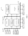
- FIG. 1 is a diagram of an example system including controllers and peripheral devices.
- FIG. 2 is a diagram of a module that combines one or more serial communication interfaces.
- FIG. 3 is a flow diagram of an example method for enabling one of the serial communication interfaces.
- FIG. 4 is a flow diagram of an example method for re-configuring a module to another serial communication interface.
- FIG. 5 is a table including examples of values for baud register and baud rates for asynchronous communication.
- serial communication protocols may be used for bus communication between a controller and peripheral components that are coupled to the controller.
- a controller incorporating the functionalities of one or more serial communication protocols, serially communicates with a peripheral component over a bus
- a serial communication protocol may be selected and the serial communication interface of the controller may provide the required settings of the selected serial communication protocol.
- Configuring the settings of a serial communication protocol on a serial communication interface may include setting the baud rate, setting the number of communication pins, setting to bi-directional (full duplex) or to single directional (half duplex) communication, selecting the master or slave status, designating transmit or receive buffers, or selecting synchronous or asynchronous mode of communication.
- the controllers may include a capacitive touch controller 120 , a microcontroller 130 , a power management module 140 , and a main processor 150 .
- the peripheral devices may include the I2C devices 112 , 114 , and 116 that may use the I2C serial communication protocol, the SMBus devices 122 , 124 , and 126 that may use the SMBus serial communication protocol, the SPI devices 132 , 134 , and 136 that may use the SPI serial communication protocol, the USART devices 152 , 154 , and 156 that may use the USART serial communication protocol, or the liquid crystal display (LCD) 110 .
- the I2C devices 112 , 114 , and 116 that may use the I2C serial communication protocol
- the SMBus devices 122 , 124 , and 126 that may use the SMBus serial communication protocol
- the SPI devices 132 , 134 , and 136 that may use the SPI serial communication protocol
- the USART devices 152 , 154 , and 156 that may use the USART serial communication protocol
- LCD liquid crystal display
- the interface bus 170 may couple the capacitive touch controller 120 , the microcontroller 130 , the power management module 140 , or the main processor 150 to the peripheral devices.
- the interface bus 170 may convey two or more parallel bits and may be used for transmitting and receiving data and/or commands between the controllers 120 , 130 , 140 , or 150 and the LCD display 110 , the I2C peripheral devices 110 , 112 - 116 , the SMBus peripheral devices 122 - 126 , the SPI peripheral devices 132 - 136 , or the USART peripheral devices 152 - 156 .
- the interface bus 170 may be used for transmitting and receiving data and/or commands using different serial communication protocols.
- peripheral devices may use different serial communication protocols.
- peripheral devices 122 - 126 may use the SMBus serial communication protocol and the peripheral devices 112 - 126 may use the I2C serial communication protocol for transmitting and receiving data and/or commands.
- the peripheral devices 132 - 136 may use the SPI serial communication protocol and the peripheral devices 152 - 156 may use the USART serial communication protocol for transmitting and receiving data and/or commands.
- the capacitive touch controller 120 , the microcontroller 130 , the power management module 140 , or the main processor 150 may include respective serial communication (SERCOM) modules 161 - 164 .
- the SERCOM module incorporates the functionality of one or more serial communication protocols and, depending on a setting, may be configured to implement one of the I2C, SMBus, SPI, or USART serial communication protocols.
- the SERCOM module is described in greater details below with respect to FIG. 2 .
- the capacitive touch controller 120 , the microcontroller 130 , the power management module 140 , or the main processor 150 may communicate with one or more peripheral devices.
- the microcontroller 130 may communicate with the I2C device 112 and may be required to implement the serial communication protocols I2C.
- the microcontroller 130 may communicate with the SMBus device 124 and may be required to implement the serial communication protocols SMBus.
- the capacitive touch controller 120 , the microcontroller 130 , the power management module 140 , or the main processor 150 may communicate with two or more peripheral devices and two or more SERCOM modules may be implemented in each controller.
- the SERCOM module 200 includes an interface module 210 , a protocol module 220 , and a serial engine module 230 .
- the SERCOM module 200 may incorporate the functionality of one or more serial communication protocols and at a time may execute only one serial communication protocol.
- the serial communication protocol may be selected based on a setting of the SERCOM module 200 .
- the SERCOM module 200 may receive a protocol setting externally and may store the received setting.
- the protocol module 220 may include one or more protocol configuration settings 224 .
- the protocol module 220 may include the configuration settings 224 for the I2C, SMBus, SPI, and USART serial communication protocols.
- the protocol module 220 may be coupled to the interface module 210 and may receive a protocol setting from the interface module. Based on the received protocol setting, one of the protocol configurations of the protocol module 220 may be selected.
- the interface module 210 may include the control and status registers 212 , the transmit and receive registers 214 , and the baud register 216 .
- the control and status registers 212 may hold the protocol setting and the protocol module 220 may receive the protocol setting from the control/status registers 212 .
- one or more settings related to the selected serial communication protocol may be stored in the control and status registers 212 . The initialization of the SERCOM module 200 is described in greater details below with respect to FIG. 3 .
- control and status registers 212 may be used to configure the SERCOM module 200 into performing as an SPI interface
- the configuration may include the SERCOM module 200 performing in master or slave modes.
- the control and status registers 212 may be used for storing all or a part of the selected protocol configuration settings 224 .
- the baud register 216 may store a baud value.
- the baud value may be used by the serial engine module 230 to calculate a baud rate.
- the baud value is a number between 0 and 65,536.
- the baud register 216 may be set when a configuration settings 224 is selected.
- the SERCOM module 200 may receive a baud value externally and may store the value in the baud register 216 .
- the transmit and receive registers 214 may be used by the serial engine module 230 as a storage buffers during transmitting and receiving data and/or commands from/to the SERCOM module 200 .
- the serial engine module 230 may be couple to the protocol module 220 and the interface module 210 and may include a baud rate generator 236 .
- the baud rate generator 236 may receive an internal clock of the SERCOM module 200 and may calculate a baud rate based on a frequency of the received internal clock and the baud value of the baud register 216 .
- the baud rate generator 236 may receive a clock external to the SERCOM module and may calculate a baud rate based on a frequency of the received external clock and the baud value of the baud register 216 .
- Table 500 of FIG. 5 shows examples of values for the baud register 216 in column 502 and the calculated baud rates (FB) for asynchronous communication in column 504 when the baud reference frequency is 48 MHz.
- the serial engine module 230 may include the transmitter 232 and the receiver 234 .
- the transmitter 232 and the receiver 234 send and receive data and/or commands based on the selected serial communication protocol and based on the selected serial communication protocol may use one or more transmit and receive registers 214 for buffering data during transmitting and receiving processes.
- the SERCOM module 200 may be coupled to a port control module 240 and the port control module 240 may be configured by the SERCOM module 200 based on the selected serial communication protocol.
- the serial engine module 230 including the transmitter 232 , the receiver 234 , and the address module 238 may be coupled to the device interface pins 242 to 244 through the port control module 240 and may communicate through the port control module 240 .
- the port control module 240 may be combined into the SERCOM module 200 and the device interface pins 242 to 244 coupled to the combined module may perform as general purpose input output (GPIO) pins and the interface bus 170 may perform as a GPIO expander.
- GPIO general purpose input output
- the serial engine module 230 may also include an address module 238 .
- the address module 238 may match an address with a mask, may match two addresses, or may match an address with an address range.
- the received data packets may include an address and the address matching of the address module 238 may be used to extract the received address and/or validate the received address with an address range.
- the SERCOM module 200 may enter into a sleep mode to conserve power consumption. In some implementations, when acting as slave the SERCOM module 200 may fully operate in sleep mode. As an example, when the SERCOM module is implementing I2C or SPI serial communication protocols in slave mode, the SERCOM module 200 may fully operate in sleep mode.
- one or more SERCOM modules 200 may be implemented as integrated circuit modules inside a processor or a controller chip.
- the SERCOM module 200 and the control module 240 may be implemented as integrated circuit modules inside a processor or a controller chip and the port control module 240 of the chip may be used to configure the device interface pins 242 to 244 .
- the SERCOM module may be implemented in baseband application processors operating at clock frequencies of 1 to 5 GHz (e.g., 1 GHz).
- a SERCOM module 200 may be reconfigured and another serial communication protocol may be selected when the SERCOM module 200 is running. The re-configuration of the SERCOM module 200 is described in greater details below with respect to FIG. 4 .
- a flow diagram for a method 300 for initializing a SERCOM module 200 is shown.
- the method 300 can be implemented by the SERCOM module 200 of FIG. 2 .
- the method includes receiving a signal to select a serial communication protocol ( 310 ).
- the signal can be received from a controller external to the SERCOM module 200 and the received signal can be saved in one of the control and status registers 212 .
- the external controller may directly set the control and status registers 212 of the SERCOM module 200 .
- a protocol is selected ( 320 ).
- the protocol module 220 may receive the selected serial communication protocol from the control and status registers 212 and based on the received selection may select one of the protocol configuration settings 224 .
- the serial communication module is configured ( 330 ).
- the SERCOM module 200 may be configured by setting the control and status registers 212 and baud register 216 , setting the port control module 240 , selecting a clock, and calculating a baud rate by the baud rate generator 236 .
- configuring the communication interface may include setting the number of communication pins, setting to bi-directional (full duplex) or single directional (half duplex) communication, selecting the master or slave status, selecting transmit or receive buffers, or selecting synchronous or asynchronous communication. In some implementations, during configuration, transmitting and receiving data and/or commands are disabled.
- the serial communication interface is enabled ( 340 ).
- the enable signal may be received from a controller external to the SERCOM module 200 .
- the external controller may directly enable the SERCOM module 200 through setting one of the control and status registers 212 .
- transmitting and receiving data and/or commands are disabled.
- the SERCOM module 200 may start transmitting and receiving data and/or commands using the selected serial communication protocol through the interface bus 170 .
- a flow diagram for a method 400 for re-configuring the serial communication protocol of an already running serial communication interface is shown.
- the method 400 can be implemented by the SERCOM module 200 of FIG. 2 .
- the method includes disabling the serial communication interface ( 410 ).
- a controller external to the SERCOM module 200 may set a value on one of the control and status registers 212 .
- the external controller may directly set the control and status registers 212 of the SERCOM module 200 and the communication may immediately stop responding.
- a signal is received to change the serial communication protocol and based on the received signal select another serial communication protocol ( 420 ).
- the signal can be received from a controller external to the SERCOM module 200 and the received signal can be saved in one of the control and status registers 212 .
- the external controller may directly set the control and status registers 212 of the SERCOM module 200 .
- the protocol module 220 may receive the selected protocol from one of the control and status registers 212 and based on the received selection may select one of the protocol configuration settings 224 .
- the communication interface is re-configured ( 430 ).
- the SERCOM module 200 may be re-configured by setting the control and status registers 212 and baud register 216 , setting the port control module 240 , selecting a clock, and calculating a baud rate by the baud rate generator 236 .
- re-configuring the communication interface may include setting the number of communication pins, setting to bi-directional (full duplex) or single directional (half duplex) communication, selecting the master or slave status, selecting transmit or receive buffers, or selecting synchronous or asynchronous communication.
- the communication interface is re-enabled ( 440 ).
- the enable signal may be received from a controller external to the SERCOM module 200 .
- the external controller may directly enable the SERCOM module through setting one of the control and status registers 212 .
- transmitting and receiving data and/or commands are disabled.
- Data is transmitted or received using the re-enabled serial communication interface ( 450 ).
- the SERCOM module 200 may start transmitting and receiving data and/or command through the interface bus 170 using the newly selected serial communication protocol.
Landscapes
- Engineering & Computer Science (AREA)
- Theoretical Computer Science (AREA)
- Physics & Mathematics (AREA)
- General Engineering & Computer Science (AREA)
- General Physics & Mathematics (AREA)
- Information Transfer Systems (AREA)
Abstract
Description
Claims (19)
Priority Applications (2)
| Application Number | Priority Date | Filing Date | Title |
|---|---|---|---|
| US14/014,128 US9772970B2 (en) | 2013-08-29 | 2013-08-29 | Multi-protocol serial communication interface |
| DE102014216167.3A DE102014216167A1 (en) | 2013-08-29 | 2014-08-14 | Serial multiprotocol communication interface |
Applications Claiming Priority (1)
| Application Number | Priority Date | Filing Date | Title |
|---|---|---|---|
| US14/014,128 US9772970B2 (en) | 2013-08-29 | 2013-08-29 | Multi-protocol serial communication interface |
Publications (2)
| Publication Number | Publication Date |
|---|---|
| US20150067206A1 US20150067206A1 (en) | 2015-03-05 |
| US9772970B2 true US9772970B2 (en) | 2017-09-26 |
Family
ID=52470671
Family Applications (1)
| Application Number | Title | Priority Date | Filing Date |
|---|---|---|---|
| US14/014,128 Active 2035-06-18 US9772970B2 (en) | 2013-08-29 | 2013-08-29 | Multi-protocol serial communication interface |
Country Status (2)
| Country | Link |
|---|---|
| US (1) | US9772970B2 (en) |
| DE (1) | DE102014216167A1 (en) |
Cited By (4)
| Publication number | Priority date | Publication date | Assignee | Title |
|---|---|---|---|---|
| TWI730465B (en) * | 2019-10-22 | 2021-06-11 | 新唐科技股份有限公司 | Serial bidirectional communication circuit and method thereof |
| US20230153263A1 (en) * | 2021-11-16 | 2023-05-18 | Infineon Technologies Austria Ag | Flexible high speed interface implementation in a power supply |
| US11729096B2 (en) | 2017-06-30 | 2023-08-15 | Intel Corporation | Techniques to support multiple protocols between computer system interconnects |
| US11782866B2 (en) | 2017-07-01 | 2023-10-10 | Intel Corporation | Techniques to support mulitple interconnect protocols for an interconnect |
Families Citing this family (12)
| Publication number | Priority date | Publication date | Assignee | Title |
|---|---|---|---|---|
| CN104539591B (en) * | 2014-12-12 | 2017-10-20 | 中国电子科技集团公司第二十二研究所 | A kind of multiple protocol bus control device |
| DE102015106024B4 (en) * | 2015-04-20 | 2023-06-07 | Interroll Holding Ag | Conveyor with configuration change |
| US9514066B1 (en) * | 2015-09-09 | 2016-12-06 | Motorola Solutions, Inc. | Reconfigurable interface and method of configuring a reconfigurable interface |
| US11249808B2 (en) | 2017-08-22 | 2022-02-15 | Intel Corporation | Connecting accelerator resources using a switch |
| CN112740191B (en) * | 2018-06-08 | 2023-03-28 | Iot耐科特有限公司 | Communication device |
| US10649945B1 (en) * | 2018-12-10 | 2020-05-12 | Analog Devices International Unlimited Company | Non-native digital interface support over a two-wire communication bus |
| US10797893B2 (en) * | 2018-12-13 | 2020-10-06 | Cisco Technology, Inc. | Single pair ethernet management interface |
| CN110727420A (en) * | 2019-09-06 | 2020-01-24 | 广东宝莱特医用科技股份有限公司 | Serial port compatible method and system |
| CN112199307A (en) * | 2020-10-26 | 2021-01-08 | 英业达科技有限公司 | Processing device with serial communication interface processing function and method thereof |
| CN114189466A (en) * | 2021-01-21 | 2022-03-15 | 青岛鼎信通讯股份有限公司 | Method for detecting local maintenance interface communication mode of low-voltage power acquisition terminal |
| CN113641614A (en) * | 2021-07-07 | 2021-11-12 | 北京智芯微电子科技有限公司 | Single-channel multi-service parallel processing method and chip based on SPI |
| CN114064532B (en) * | 2021-11-08 | 2022-06-17 | 深圳华云信息系统有限公司 | Data processing method and device, electronic equipment and storage medium |
Citations (5)
| Publication number | Priority date | Publication date | Assignee | Title |
|---|---|---|---|---|
| US4570217A (en) * | 1982-03-29 | 1986-02-11 | Allen Bruce S | Man machine interface |
| US20050172059A1 (en) * | 2004-01-07 | 2005-08-04 | Hitachi, Ltd. | Data communication system and controller |
| US20080027587A1 (en) * | 2003-12-23 | 2008-01-31 | Rain Bird Corporation | Code replacement for irrigation controllers |
| US20090132751A1 (en) * | 2007-11-21 | 2009-05-21 | Microchip Technology Incorporated | Ethernet Controller |
| US20130290577A1 (en) * | 2012-04-30 | 2013-10-31 | Freescale Semiconductor, Inc. | Method the configure serial communications and device thereof |
-
2013
- 2013-08-29 US US14/014,128 patent/US9772970B2/en active Active
-
2014
- 2014-08-14 DE DE102014216167.3A patent/DE102014216167A1/en active Pending
Patent Citations (5)
| Publication number | Priority date | Publication date | Assignee | Title |
|---|---|---|---|---|
| US4570217A (en) * | 1982-03-29 | 1986-02-11 | Allen Bruce S | Man machine interface |
| US20080027587A1 (en) * | 2003-12-23 | 2008-01-31 | Rain Bird Corporation | Code replacement for irrigation controllers |
| US20050172059A1 (en) * | 2004-01-07 | 2005-08-04 | Hitachi, Ltd. | Data communication system and controller |
| US20090132751A1 (en) * | 2007-11-21 | 2009-05-21 | Microchip Technology Incorporated | Ethernet Controller |
| US20130290577A1 (en) * | 2012-04-30 | 2013-10-31 | Freescale Semiconductor, Inc. | Method the configure serial communications and device thereof |
Cited By (4)
| Publication number | Priority date | Publication date | Assignee | Title |
|---|---|---|---|---|
| US11729096B2 (en) | 2017-06-30 | 2023-08-15 | Intel Corporation | Techniques to support multiple protocols between computer system interconnects |
| US11782866B2 (en) | 2017-07-01 | 2023-10-10 | Intel Corporation | Techniques to support mulitple interconnect protocols for an interconnect |
| TWI730465B (en) * | 2019-10-22 | 2021-06-11 | 新唐科技股份有限公司 | Serial bidirectional communication circuit and method thereof |
| US20230153263A1 (en) * | 2021-11-16 | 2023-05-18 | Infineon Technologies Austria Ag | Flexible high speed interface implementation in a power supply |
Also Published As
| Publication number | Publication date |
|---|---|
| US20150067206A1 (en) | 2015-03-05 |
| DE102014216167A1 (en) | 2015-03-05 |
Similar Documents
| Publication | Publication Date | Title |
|---|---|---|
| US9772970B2 (en) | Multi-protocol serial communication interface | |
| US20170168966A1 (en) | Optimal latency packetizer finite state machine for messaging and input/output transfer interfaces | |
| Blessington et al. | Optimal implementation of UART-SPI Interface in SoC | |
| EP2950219B1 (en) | Method and apparatus for using serial port in time division multiplexing manner | |
| CN108647180B (en) | Operation system and corresponding electronic equipment | |
| CN104156333A (en) | FPGA-based UART multi-interface extension system and method | |
| CN104714908A (en) | SPI capable of supporting master/slave mode | |
| WO2019072218A1 (en) | Method and device for signal conversion, home bus system (hbs) circuit, and user equipment | |
| EP2972925B1 (en) | Two-wire serial interface and protocol | |
| US8639851B2 (en) | Serial bit processor | |
| US8626972B2 (en) | I2C multi-slot circuit system and method for transmitting I2C signals | |
| CN106776425B (en) | A kind of working frequency setting method, main control card, service card and communication equipment | |
| CN104156335A (en) | Method for multiplexing multiple UART interfaces | |
| CN106788808A (en) | A kind of radio signal quality detector and method | |
| KR20150103905A (en) | Method and apparatus for switching between master MCU(micro controller unit) and slave MCU of dual MCU | |
| CN103617145B (en) | A kind of self-defined bus and its implementation | |
| US20180357067A1 (en) | In-band hardware reset for virtual general purpose input/output interface | |
| CN203984449U (en) | A kind of portable gateway module | |
| CN107918443B (en) | Signal generation method and device | |
| WO2018006777A1 (en) | Communication connection apparatus and method, and communication board | |
| CN110471881B (en) | Method for realizing rapid communication between multiple slave devices and SPI (Serial peripheral interface) master device | |
| US20170302319A1 (en) | Wearable devices and methods for data transmission and reception therewith | |
| CN103473192A (en) | Field programmable gate array and soft-core processor core-based multi-UART (universal asynchronous receiver transmitter) interface extension system | |
| CN109739695B (en) | ARM and FPGA dissimilar redundancy communication method in unmanned aerial vehicle controller | |
| CN213211018U (en) | Signal processing board card |
Legal Events
| Date | Code | Title | Description |
|---|---|---|---|
| AS | Assignment |
Owner name: ATMEL CORPORATION, CALIFORNIA Free format text: ASSIGNMENT OF ASSIGNORS INTEREST;ASSIGNORS:LUO, YONG;FULLERTON, IAN;FROEMMING, BENJAMIN FRANCIS;AND OTHERS;SIGNING DATES FROM 20130828 TO 20130829;REEL/FRAME:031114/0340 |
|
| AS | Assignment |
Owner name: MORGAN STANLEY SENIOR FUNDING, INC. AS ADMINISTRATIVE AGENT, NEW YORK Free format text: PATENT SECURITY AGREEMENT;ASSIGNOR:ATMEL CORPORATION;REEL/FRAME:031912/0173 Effective date: 20131206 Owner name: MORGAN STANLEY SENIOR FUNDING, INC. AS ADMINISTRAT Free format text: PATENT SECURITY AGREEMENT;ASSIGNOR:ATMEL CORPORATION;REEL/FRAME:031912/0173 Effective date: 20131206 |
|
| AS | Assignment |
Owner name: ATMEL CORPORATION, CALIFORNIA Free format text: TERMINATION AND RELEASE OF SECURITY INTEREST IN PATENT COLLATERAL;ASSIGNOR:MORGAN STANLEY SENIOR FUNDING, INC.;REEL/FRAME:038376/0001 Effective date: 20160404 |
|
| AS | Assignment |
Owner name: JPMORGAN CHASE BANK, N.A., AS ADMINISTRATIVE AGENT, ILLINOIS Free format text: SECURITY INTEREST;ASSIGNOR:ATMEL CORPORATION;REEL/FRAME:041715/0747 Effective date: 20170208 Owner name: JPMORGAN CHASE BANK, N.A., AS ADMINISTRATIVE AGENT Free format text: SECURITY INTEREST;ASSIGNOR:ATMEL CORPORATION;REEL/FRAME:041715/0747 Effective date: 20170208 |
|
| STCF | Information on status: patent grant |
Free format text: PATENTED CASE |
|
| AS | Assignment |
Owner name: JPMORGAN CHASE BANK, N.A., AS ADMINISTRATIVE AGENT, ILLINOIS Free format text: SECURITY INTEREST;ASSIGNORS:MICROCHIP TECHNOLOGY INCORPORATED;SILICON STORAGE TECHNOLOGY, INC.;ATMEL CORPORATION;AND OTHERS;REEL/FRAME:046426/0001 Effective date: 20180529 Owner name: JPMORGAN CHASE BANK, N.A., AS ADMINISTRATIVE AGENT Free format text: SECURITY INTEREST;ASSIGNORS:MICROCHIP TECHNOLOGY INCORPORATED;SILICON STORAGE TECHNOLOGY, INC.;ATMEL CORPORATION;AND OTHERS;REEL/FRAME:046426/0001 Effective date: 20180529 |
|
| AS | Assignment |
Owner name: MICROCHIP TECHNOLOGY INCORPORATED, ARIZONA Free format text: ASSIGNMENT OF ASSIGNORS INTEREST;ASSIGNOR:ATMEL CORPORATION;REEL/FRAME:046874/0877 Effective date: 20180913 |
|
| AS | Assignment |
Owner name: WELLS FARGO BANK, NATIONAL ASSOCIATION, AS NOTES COLLATERAL AGENT, CALIFORNIA Free format text: SECURITY INTEREST;ASSIGNORS:MICROCHIP TECHNOLOGY INCORPORATED;SILICON STORAGE TECHNOLOGY, INC.;ATMEL CORPORATION;AND OTHERS;REEL/FRAME:047103/0206 Effective date: 20180914 Owner name: WELLS FARGO BANK, NATIONAL ASSOCIATION, AS NOTES C Free format text: SECURITY INTEREST;ASSIGNORS:MICROCHIP TECHNOLOGY INCORPORATED;SILICON STORAGE TECHNOLOGY, INC.;ATMEL CORPORATION;AND OTHERS;REEL/FRAME:047103/0206 Effective date: 20180914 |
|
| IPR | Aia trial proceeding filed before the patent and appeal board: inter partes review |
Free format text: TRIAL NO: IPR2020-00367 Opponent name: NUVOTON TECHNOLOGY CORPORATION ANDNUVOTON TECHNOLOGY CORPORATION AMERICA Effective date: 20191230 |
|
| AS | Assignment |
Owner name: JPMORGAN CHASE BANK, N.A., AS ADMINISTRATIVE AGENT, DELAWARE Free format text: SECURITY INTEREST;ASSIGNORS:MICROCHIP TECHNOLOGY INC.;SILICON STORAGE TECHNOLOGY, INC.;ATMEL CORPORATION;AND OTHERS;REEL/FRAME:053311/0305 Effective date: 20200327 |
|
| AS | Assignment |
Owner name: ATMEL CORPORATION, ARIZONA Free format text: RELEASE BY SECURED PARTY;ASSIGNOR:JPMORGAN CHASE BANK, N.A, AS ADMINISTRATIVE AGENT;REEL/FRAME:053466/0011 Effective date: 20200529 Owner name: MICROCHIP TECHNOLOGY INC., ARIZONA Free format text: RELEASE BY SECURED PARTY;ASSIGNOR:JPMORGAN CHASE BANK, N.A, AS ADMINISTRATIVE AGENT;REEL/FRAME:053466/0011 Effective date: 20200529 Owner name: MICROSEMI STORAGE SOLUTIONS, INC., ARIZONA Free format text: RELEASE BY SECURED PARTY;ASSIGNOR:JPMORGAN CHASE BANK, N.A, AS ADMINISTRATIVE AGENT;REEL/FRAME:053466/0011 Effective date: 20200529 Owner name: MICROSEMI CORPORATION, CALIFORNIA Free format text: RELEASE BY SECURED PARTY;ASSIGNOR:JPMORGAN CHASE BANK, N.A, AS ADMINISTRATIVE AGENT;REEL/FRAME:053466/0011 Effective date: 20200529 Owner name: SILICON STORAGE TECHNOLOGY, INC., ARIZONA Free format text: RELEASE BY SECURED PARTY;ASSIGNOR:JPMORGAN CHASE BANK, N.A, AS ADMINISTRATIVE AGENT;REEL/FRAME:053466/0011 Effective date: 20200529 |
|
| AS | Assignment |
Owner name: WELLS FARGO BANK, NATIONAL ASSOCIATION, MINNESOTA Free format text: SECURITY INTEREST;ASSIGNORS:MICROCHIP TECHNOLOGY INC.;SILICON STORAGE TECHNOLOGY, INC.;ATMEL CORPORATION;AND OTHERS;REEL/FRAME:053468/0705 Effective date: 20200529 |
|
| AS | Assignment |
Owner name: WELLS FARGO BANK, NATIONAL ASSOCIATION, AS COLLATERAL AGENT, MINNESOTA Free format text: SECURITY INTEREST;ASSIGNORS:MICROCHIP TECHNOLOGY INCORPORATED;SILICON STORAGE TECHNOLOGY, INC.;ATMEL CORPORATION;AND OTHERS;REEL/FRAME:055671/0612 Effective date: 20201217 |
|
| MAFP | Maintenance fee payment |
Free format text: PAYMENT OF MAINTENANCE FEE, 4TH YEAR, LARGE ENTITY (ORIGINAL EVENT CODE: M1551); ENTITY STATUS OF PATENT OWNER: LARGE ENTITY Year of fee payment: 4 |
|
| AS | Assignment |
Owner name: WELLS FARGO BANK, NATIONAL ASSOCIATION, AS NOTES COLLATERAL AGENT, MINNESOTA Free format text: SECURITY INTEREST;ASSIGNORS:MICROCHIP TECHNOLOGY INCORPORATED;SILICON STORAGE TECHNOLOGY, INC.;ATMEL CORPORATION;AND OTHERS;REEL/FRAME:057935/0474 Effective date: 20210528 |
|
| AS | Assignment |
Owner name: MICROSEMI STORAGE SOLUTIONS, INC., ARIZONA Free format text: RELEASE BY SECURED PARTY;ASSIGNOR:JPMORGAN CHASE BANK, N.A., AS ADMINISTRATIVE AGENT;REEL/FRAME:059333/0222 Effective date: 20220218 Owner name: MICROSEMI CORPORATION, ARIZONA Free format text: RELEASE BY SECURED PARTY;ASSIGNOR:JPMORGAN CHASE BANK, N.A., AS ADMINISTRATIVE AGENT;REEL/FRAME:059333/0222 Effective date: 20220218 Owner name: ATMEL CORPORATION, ARIZONA Free format text: RELEASE BY SECURED PARTY;ASSIGNOR:JPMORGAN CHASE BANK, N.A., AS ADMINISTRATIVE AGENT;REEL/FRAME:059333/0222 Effective date: 20220218 Owner name: SILICON STORAGE TECHNOLOGY, INC., ARIZONA Free format text: RELEASE BY SECURED PARTY;ASSIGNOR:JPMORGAN CHASE BANK, N.A., AS ADMINISTRATIVE AGENT;REEL/FRAME:059333/0222 Effective date: 20220218 Owner name: MICROCHIP TECHNOLOGY INCORPORATED, ARIZONA Free format text: RELEASE BY SECURED PARTY;ASSIGNOR:JPMORGAN CHASE BANK, N.A., AS ADMINISTRATIVE AGENT;REEL/FRAME:059333/0222 Effective date: 20220218 |
|
| AS | Assignment |
Owner name: ATMEL CORPORATION, ARIZONA Free format text: RELEASE BY SECURED PARTY;ASSIGNOR:JPMORGAN CHASE BANK, N.A., AS ADMINISTRATIVE AGENT;REEL/FRAME:059262/0105 Effective date: 20220218 |
|
| AS | Assignment |
Owner name: MICROSEMI STORAGE SOLUTIONS, INC., ARIZONA Free format text: RELEASE BY SECURED PARTY;ASSIGNOR:WELLS FARGO BANK, NATIONAL ASSOCIATION, AS NOTES COLLATERAL AGENT;REEL/FRAME:059358/0001 Effective date: 20220228 Owner name: MICROSEMI CORPORATION, ARIZONA Free format text: RELEASE BY SECURED PARTY;ASSIGNOR:WELLS FARGO BANK, NATIONAL ASSOCIATION, AS NOTES COLLATERAL AGENT;REEL/FRAME:059358/0001 Effective date: 20220228 Owner name: ATMEL CORPORATION, ARIZONA Free format text: RELEASE BY SECURED PARTY;ASSIGNOR:WELLS FARGO BANK, NATIONAL ASSOCIATION, AS NOTES COLLATERAL AGENT;REEL/FRAME:059358/0001 Effective date: 20220228 Owner name: SILICON STORAGE TECHNOLOGY, INC., ARIZONA Free format text: RELEASE BY SECURED PARTY;ASSIGNOR:WELLS FARGO BANK, NATIONAL ASSOCIATION, AS NOTES COLLATERAL AGENT;REEL/FRAME:059358/0001 Effective date: 20220228 Owner name: MICROCHIP TECHNOLOGY INCORPORATED, ARIZONA Free format text: RELEASE BY SECURED PARTY;ASSIGNOR:WELLS FARGO BANK, NATIONAL ASSOCIATION, AS NOTES COLLATERAL AGENT;REEL/FRAME:059358/0001 Effective date: 20220228 |
|
| AS | Assignment |
Owner name: MICROSEMI STORAGE SOLUTIONS, INC., ARIZONA Free format text: RELEASE BY SECURED PARTY;ASSIGNOR:WELLS FARGO BANK, NATIONAL ASSOCIATION, AS NOTES COLLATERAL AGENT;REEL/FRAME:059863/0400 Effective date: 20220228 Owner name: MICROSEMI CORPORATION, ARIZONA Free format text: RELEASE BY SECURED PARTY;ASSIGNOR:WELLS FARGO BANK, NATIONAL ASSOCIATION, AS NOTES COLLATERAL AGENT;REEL/FRAME:059863/0400 Effective date: 20220228 Owner name: ATMEL CORPORATION, ARIZONA Free format text: RELEASE BY SECURED PARTY;ASSIGNOR:WELLS FARGO BANK, NATIONAL ASSOCIATION, AS NOTES COLLATERAL AGENT;REEL/FRAME:059863/0400 Effective date: 20220228 Owner name: SILICON STORAGE TECHNOLOGY, INC., ARIZONA Free format text: RELEASE BY SECURED PARTY;ASSIGNOR:WELLS FARGO BANK, NATIONAL ASSOCIATION, AS NOTES COLLATERAL AGENT;REEL/FRAME:059863/0400 Effective date: 20220228 Owner name: MICROCHIP TECHNOLOGY INCORPORATED, ARIZONA Free format text: RELEASE BY SECURED PARTY;ASSIGNOR:WELLS FARGO BANK, NATIONAL ASSOCIATION, AS NOTES COLLATERAL AGENT;REEL/FRAME:059863/0400 Effective date: 20220228 |
|
| AS | Assignment |
Owner name: MICROSEMI STORAGE SOLUTIONS, INC., ARIZONA Free format text: RELEASE BY SECURED PARTY;ASSIGNOR:WELLS FARGO BANK, NATIONAL ASSOCIATION, AS NOTES COLLATERAL AGENT;REEL/FRAME:059363/0001 Effective date: 20220228 Owner name: MICROSEMI CORPORATION, ARIZONA Free format text: RELEASE BY SECURED PARTY;ASSIGNOR:WELLS FARGO BANK, NATIONAL ASSOCIATION, AS NOTES COLLATERAL AGENT;REEL/FRAME:059363/0001 Effective date: 20220228 Owner name: ATMEL CORPORATION, ARIZONA Free format text: RELEASE BY SECURED PARTY;ASSIGNOR:WELLS FARGO BANK, NATIONAL ASSOCIATION, AS NOTES COLLATERAL AGENT;REEL/FRAME:059363/0001 Effective date: 20220228 Owner name: SILICON STORAGE TECHNOLOGY, INC., ARIZONA Free format text: RELEASE BY SECURED PARTY;ASSIGNOR:WELLS FARGO BANK, NATIONAL ASSOCIATION, AS NOTES COLLATERAL AGENT;REEL/FRAME:059363/0001 Effective date: 20220228 Owner name: MICROCHIP TECHNOLOGY INCORPORATED, ARIZONA Free format text: RELEASE BY SECURED PARTY;ASSIGNOR:WELLS FARGO BANK, NATIONAL ASSOCIATION, AS NOTES COLLATERAL AGENT;REEL/FRAME:059363/0001 Effective date: 20220228 |
|
| AS | Assignment |
Owner name: MICROSEMI STORAGE SOLUTIONS, INC., ARIZONA Free format text: RELEASE BY SECURED PARTY;ASSIGNOR:WELLS FARGO BANK, NATIONAL ASSOCIATION, AS NOTES COLLATERAL AGENT;REEL/FRAME:060894/0437 Effective date: 20220228 Owner name: MICROSEMI CORPORATION, ARIZONA Free format text: RELEASE BY SECURED PARTY;ASSIGNOR:WELLS FARGO BANK, NATIONAL ASSOCIATION, AS NOTES COLLATERAL AGENT;REEL/FRAME:060894/0437 Effective date: 20220228 Owner name: ATMEL CORPORATION, ARIZONA Free format text: RELEASE BY SECURED PARTY;ASSIGNOR:WELLS FARGO BANK, NATIONAL ASSOCIATION, AS NOTES COLLATERAL AGENT;REEL/FRAME:060894/0437 Effective date: 20220228 Owner name: SILICON STORAGE TECHNOLOGY, INC., ARIZONA Free format text: RELEASE BY SECURED PARTY;ASSIGNOR:WELLS FARGO BANK, NATIONAL ASSOCIATION, AS NOTES COLLATERAL AGENT;REEL/FRAME:060894/0437 Effective date: 20220228 Owner name: MICROCHIP TECHNOLOGY INCORPORATED, ARIZONA Free format text: RELEASE BY SECURED PARTY;ASSIGNOR:WELLS FARGO BANK, NATIONAL ASSOCIATION, AS NOTES COLLATERAL AGENT;REEL/FRAME:060894/0437 Effective date: 20220228 |