US9740559B2 - Systems and methods for compaction based flash memory data recovery - Google Patents
Systems and methods for compaction based flash memory data recovery Download PDFInfo
- Publication number
- US9740559B2 US9740559B2 US14/925,726 US201514925726A US9740559B2 US 9740559 B2 US9740559 B2 US 9740559B2 US 201514925726 A US201514925726 A US 201514925726A US 9740559 B2 US9740559 B2 US 9740559B2
- Authority
- US
- United States
- Prior art keywords
- groups
- output
- binary values
- binary
- compacted
- Prior art date
- Legal status (The legal status is an assumption and is not a legal conclusion. Google has not performed a legal analysis and makes no representation as to the accuracy of the status listed.)
- Active, expires
Links
Images
Classifications
-
- G—PHYSICS
- G06—COMPUTING; CALCULATING OR COUNTING
- G06F—ELECTRIC DIGITAL DATA PROCESSING
- G06F11/00—Error detection; Error correction; Monitoring
- G06F11/07—Responding to the occurrence of a fault, e.g. fault tolerance
- G06F11/08—Error detection or correction by redundancy in data representation, e.g. by using checking codes
- G06F11/10—Adding special bits or symbols to the coded information, e.g. parity check, casting out 9's or 11's
- G06F11/1008—Adding special bits or symbols to the coded information, e.g. parity check, casting out 9's or 11's in individual solid state devices
- G06F11/1068—Adding special bits or symbols to the coded information, e.g. parity check, casting out 9's or 11's in individual solid state devices in sector programmable memories, e.g. flash disk
-
- G—PHYSICS
- G06—COMPUTING; CALCULATING OR COUNTING
- G06F—ELECTRIC DIGITAL DATA PROCESSING
- G06F11/00—Error detection; Error correction; Monitoring
- G06F11/07—Responding to the occurrence of a fault, e.g. fault tolerance
- G06F11/08—Error detection or correction by redundancy in data representation, e.g. by using checking codes
- G06F11/10—Adding special bits or symbols to the coded information, e.g. parity check, casting out 9's or 11's
- G06F11/1008—Adding special bits or symbols to the coded information, e.g. parity check, casting out 9's or 11's in individual solid state devices
- G06F11/1012—Adding special bits or symbols to the coded information, e.g. parity check, casting out 9's or 11's in individual solid state devices using codes or arrangements adapted for a specific type of error
-
- G—PHYSICS
- G11—INFORMATION STORAGE
- G11C—STATIC STORES
- G11C29/00—Checking stores for correct operation ; Subsequent repair; Testing stores during standby or offline operation
- G11C29/52—Protection of memory contents; Detection of errors in memory contents
-
- H—ELECTRICITY
- H03—ELECTRONIC CIRCUITRY
- H03M—CODING; DECODING; CODE CONVERSION IN GENERAL
- H03M13/00—Coding, decoding or code conversion, for error detection or error correction; Coding theory basic assumptions; Coding bounds; Error probability evaluation methods; Channel models; Simulation or testing of codes
- H03M13/03—Error detection or forward error correction by redundancy in data representation, i.e. code words containing more digits than the source words
- H03M13/05—Error detection or forward error correction by redundancy in data representation, i.e. code words containing more digits than the source words using block codes, i.e. a predetermined number of check bits joined to a predetermined number of information bits
- H03M13/11—Error detection or forward error correction by redundancy in data representation, i.e. code words containing more digits than the source words using block codes, i.e. a predetermined number of check bits joined to a predetermined number of information bits using multiple parity bits
- H03M13/1102—Codes on graphs and decoding on graphs, e.g. low-density parity check [LDPC] codes
- H03M13/1105—Decoding
- H03M13/1111—Soft-decision decoding, e.g. by means of message passing or belief propagation algorithms
-
- H—ELECTRICITY
- H03—ELECTRONIC CIRCUITRY
- H03M—CODING; DECODING; CODE CONVERSION IN GENERAL
- H03M13/00—Coding, decoding or code conversion, for error detection or error correction; Coding theory basic assumptions; Coding bounds; Error probability evaluation methods; Channel models; Simulation or testing of codes
- H03M13/65—Purpose and implementation aspects
- H03M13/6577—Representation or format of variables, register sizes or word-lengths and quantization
- H03M13/6588—Compression or short representation of variables
-
- H—ELECTRICITY
- H03—ELECTRONIC CIRCUITRY
- H03M—CODING; DECODING; CODE CONVERSION IN GENERAL
- H03M7/00—Conversion of a code where information is represented by a given sequence or number of digits to a code where the same, similar or subset of information is represented by a different sequence or number of digits
-
- G—PHYSICS
- G06—COMPUTING; CALCULATING OR COUNTING
- G06F—ELECTRIC DIGITAL DATA PROCESSING
- G06F2212/00—Indexing scheme relating to accessing, addressing or allocation within memory systems or architectures
- G06F2212/40—Specific encoding of data in memory or cache
- G06F2212/401—Compressed data
-
- G—PHYSICS
- G06—COMPUTING; CALCULATING OR COUNTING
- G06F—ELECTRIC DIGITAL DATA PROCESSING
- G06F2212/00—Indexing scheme relating to accessing, addressing or allocation within memory systems or architectures
- G06F2212/40—Specific encoding of data in memory or cache
- G06F2212/403—Error protection encoding, e.g. using parity or ECC codes
Definitions
- Embodiments are related to systems and methods for data storage, and more particularly to systems and methods for storing data to and accessing data from a flash memory.
- multi-level cells are used. Such multi-level cells may be, for example, programmed to with one of four voltage levels with each of the four voltage levels representing a two bit binary value.
- a read back voltage is compared with a center voltage threshold to determine the least significant bit of the two bit binary value and additional comparisons are performed with an upper voltage threshold and a lower voltage threshold to determine the most significant bit of the two bit binary value.
- Use of multiple comparisons to yield the two bit binary value results in considerable latency.
- Embodiments are related to systems and methods for data storage, and more particularly to systems and methods for storing data to and accessing data from a flash memory.
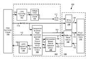
- FIG. 1 a shows a solid state storage system including a compaction based partial decoder circuit implemented on a semiconductor die apart from flash memory cells in accordance with some embodiments of the present invention
- FIG. 1 b shows a solid state storage system including a compaction based partial decoder circuit implemented on a semiconductor die along with flash memory cells in accordance with some embodiments of the present invention
- FIG. 2 shows an example of multi-level cell encoding using multiple low density parity check codewords in accordance with some embodiments of the present invention
- FIG. 3 shows a five bit word to three voltage levels conversion table in accordance with some embodiments of the present invention
- FIG. 4 a shows another five bit word to three voltage levels conversion table in accordance with some embodiments of the present invention.
- FIG. 4 b shows a map corresponding to a lower threshold resolution of voltage levels of non-compacted hard data to soft data conversion in accordance with various embodiments of the present invention
- FIG. 4 c shows a map corresponding to the lower threshold resolution of voltage levels of three bit compacted hard data to two bit soft data conversion in accordance with various embodiments of the present invention
- FIG. 4 d shows a map corresponding to a center threshold resolution of voltage levels of non-compacted hard data to soft data conversion in accordance with various embodiments of the present invention
- FIG. 4 e shows a map corresponding to an upper threshold resolution of voltage levels of non-compacted hard data to soft data conversion in accordance with various embodiments of the present invention.
- FIG. 5 shows a more detailed example of a solid state storage system including a compaction based partial decoder circuit in accordance with some embodiments of the present invention.
- Embodiments are related to systems and methods for data storage, and more particularly to systems and methods for storing data to and accessing data from a flash memory.
- Various embodiments of the present invention provide systems for accessing a flash memory device.
- the systems include a data read circuit, a compaction based partial decoder circuit, and a first data decoding circuit.
- the data read circuit is operable to compare voltages read from a set of M groups of N flash memory cells with a first threshold value to yield a binary output set.
- the binary output set includes a set of M groups of N binary values where M and N are integers.
- the compaction based partial decoder circuit is operable to compact a subset of the M groups of N binary values to yield a compacted output.
- the compacted output is represented in fewer bits than required to represent the subset of the M groups of N binary values.
- the first data decoding circuit is operable to generate at least one soft data value based upon the compacted output.
- the soft data value corresponds to an element of a given codeword represented by the M groups of N binary values.
- the systems are implemented in one or more semiconductor devices.
- the compaction based partial decoder circuit is further operable to repeatedly compact additional subsets of the M groups of N binary values to yield additional compacted outputs.
- the first decoder circuit is further operable to generate at least one additional soft data value based upon each of the respective additional compacted outputs.
- the system further includes a second data decoding circuit operable to apply a data decoding algorithm to the given codeword to yield a decoded output.
- the given codeword may be a low density parity check codeword
- the second data decoding circuit may be a low density parity check decoding circuit.
- N is three, the subset of the M groups of N binary values is one group of the N binary values, and the compacted output is a two bit ternary number.
- N is three, the subset of the M groups of N binary values is three groups of the N binary values, and the compacted output is a five bit ternary number.
- N is three, the subset of the M groups of N binary values is five groups of the N binary values, and the compacted output is an eight bit ternary number.
- the given codeword is a first codeword
- the at least one soft data value is a first soft data value
- the binary output set is a first binary output set
- the data read circuit is further operable to compare voltages read from the set of M groups of N flash memory cells with a second threshold value to yield a second binary output set
- the first data decoding circuit is further operable to: generate at least a second soft data value directly from the second binary output set, where the second soft data value corresponds to an element of a second codeword represented by the M groups of N binary values.
- the first data decoding circuit includes: a first look-up table including soft data values corresponding to respective values of the compacted output; and a second look-up table including soft data values corresponding to respective values of the N binary values.
- the set of M groups of N binary values is a first set of M groups of N binary values
- the given codeword is a first codeword
- the at least one soft data value is a first soft data value
- the binary output set is a first binary output set
- the data read circuit is further operable to compare voltages read from the set of M groups of N flash memory cells with a second threshold value to yield a second binary output set
- the compaction based partial decoder circuit is further operable to compact a subset of a second set of M groups of N binary values to yield a second compacted output, where the second compacted output is represented in fewer bits than required to represent the subset of the second set of M groups of N binary values.
- the first data decoding circuit is further operable to generate at least a second soft data value directly from the second binary output set, where the second soft data value corresponds to an element of a second codeword represented by the M groups of N binary values.
- the first data decoding circuit includes: a first look-up table including soft data values corresponding to respective values of the first compacted output; and a second look-up table including soft data values corresponding to respective values of the first compacted output.
- the methods include: accessing a set of M groups of N flash memory cells to yield M groups of N voltages, and wherein M and N are integers; using a read circuit to compare the M groups of N voltages with a first threshold value to yield a binary output set, wherein the binary output set includes a set of M groups of N binary values; compacting a subset of the M groups of N binary values to yield a compacted output, wherein the compacted output is represented in fewer bits than required to represent the subset of the M groups of N binary values; and generating at least one soft data value based upon the compacted output, wherein the soft data value corresponds to an element of a given codeword represented by the M groups of N binary values.
- N is three, the subset of the M groups of N binary values is one group of the N binary values, and the compacted output is a two bit ternary number.
- N is three, the subset of the M groups of N binary values is three groups of the N binary values, and the compacted output is a five bit ternary number.
- N is three, the subset of the M groups of N binary values is five groups of the N binary values, and the compacted output is an eight bit ternary number.
- the subset of the M groups of N binary values is a first subset of the M groups of N binary values
- the compacted output is a first compacted output.
- the methods further include: repeatedly compacting additional subsets of the M groups of N binary values to yield corresponding additional compacted outputs; generating at least one additional soft data value based upon each of the respective additional compacted outputs; and applying a data decoding algorithm to the given codeword to yield a decoded output.
- Solid state storage system 100 includes a compaction based partial decoder circuit 198 implemented on a semiconductor die 102 apart from a semiconductor die 104 where flash memory cells 140 are implemented in accordance with some embodiments of the present invention.
- Solid state storage system 100 includes a host controller circuit 195 , a low density parity check encoding circuit 105 , a voltage value encoding circuit 109 , a write circuit 130 , flash memory cells 140 , a buffering read circuit 150 , a compaction enabled read controller and soft data output voltage value decoding circuit 180 , and a low density parity check decoding circuit 190 .
- Host controller circuit 195 directs read and write access to flash memory cells 140 .
- Flash memory cells 140 may be NAND flash memory cells or another type of solid state memory cells as are known in the art.
- Solid state storage system 100 is implemented using at least two distinct semiconductor dies.
- Semiconductor die 102 includes low density parity check encoding circuit 105 , voltage value encoding circuit 109 , compaction based partial decoder circuit 198 , compaction enabled read controller and soft data output voltage value decoding circuit 180 , and low density parity check decoding circuit 190 .
- Semiconductor die 104 includes write circuit 130 , flash memory cells 140 , and buffering read circuit 150 .
- solid state storage system 100 is shown as distributed across two or more semiconductor dies, that other embodiments of the present invention may be implemented with a semiconductor die that includes all of low density parity check encoding circuit 105 , voltage value encoding circuit 109 , write circuit 130 , flash memory cells 140 , buffering read circuit 150 , compaction enabled read controller and soft data output voltage value decoding circuit 180 , and low density parity check decoding circuit 190 .
- a data write is effectuated when host controller circuit 195 provides input data 103 to low density parity check encoding circuit 105 .
- Low density parity check encoding circuit 105 applies a low density parity check encoding algorithm to input data 103 to yield LDPC codewords 107 .
- LDPC codewords 107 are provided to voltage value encoding circuit 109 .
- Voltage value encoding circuit 109 applies multi-level cell encoding to a group of LDPC codewords 107 to yield write data 111 .
- five LDPC codewords are encoded together to yield write data 111 that is directed to flash memory cells 140 that are written as two-bit cells. It should be noted that while the various embodiments are discussed in relation to using a low density parity check encoding/decoding algorithm, that other encoding/decoding algorithms known in the art may be used in accordance with other embodiments of the present invention.
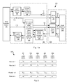
- FIG. 2 an example of multi-level cell encoding 200 using multiple low density parity check codewords 201 , 203 , 205 , 207 , 209 to yield a series of five bit words that are encoded into write data in accordance with some embodiments of the present invention.
- Each of the low density parity check codewords 201 , 203 , 205 , 207 , 209 includes a number of bits indicated as positions (i.e., position 1 , position 2 , . . . position n ⁇ 1, and position n). It should be noted that an element (e.g., bit) of each of the respective codewords is found at each position.
- a five bit word includes the first element of each of the five low density parity check codewords 201 , 203 , 205 , 207 , 209 (i.e., ⁇ A 1 , B 1 , C 1 , D 1 , E 1 ⁇ ). This is repeated for each of the positions 1 through n to yield n five bit words (i.e., ⁇ A 2 , B 2 , C 2 , D 2 , E 2 ⁇ . . . ⁇ A n , B n , C n , D n , E n ⁇ ).
- voltage value encoding circuit 109 encodes each of the n five bit words discussed in relation to FIG. 2 to a corresponding three value output that is provided as write data 111 .
- a five bit word 301 a , 301 b ( ⁇ A, B, C, D, E ⁇ ) to three voltage levels 303 a , 303 b ( ⁇ X, Y, Z ⁇ ) conversion table 300 is shown in accordance with some embodiments of the present invention.
- five bit word 301 a , 301 b correspond to the five bit words ( ⁇ A, B, C, D, E ⁇ ) discussed above in relation to FIG. 2 .
- FIG. 4 a another five bit word 401 a , 401 b ( ⁇ A, B, C, D, E ⁇ ) to three voltage levels 403 a , 403 b ( ⁇ X, Y, Z ⁇ ) conversion table 400 in accordance with some embodiments of the present invention.
- five bit word 401 a , 401 b correspond to the five bit words ( ⁇ A, B, C, D, E ⁇ ) discussed above in relation to FIG. 2 .
- the corresponding three voltage levels are “2, 2, 0”.
- three voltage levels are “3, 1, 2”
- the corresponding five bit word is ‘10101’.
- the aforementioned conversion tables are from five bit words to three voltage levels, other conversions may be possible in accordance with various embodiments of the present invention.
- other embodiments of the present invention may use conversion tables from four bit words to three voltage levels. Based upon the disclosure provided herein, one of ordinary skill in the art will recognize other conversion tables that may be used in accordance with various embodiments of the present invention.
- write data 111 is provided to a write circuit 130 .
- write circuit 130 receives an address 110 is received from host controller circuit 195 .
- Write circuit 130 converts the voltage levels (e.g., ⁇ X, Y, Z ⁇ ) received as write data 111 into a series of voltages 135 that are written to three cells of flash memory cells 140 indicated by address 110 .
- a voltage level of “0” results in voltage 135 being set below a lower threshold (V L )
- a voltage level of “1” results in voltage 135 being set above the lower threshold (V L ) and below a center threshold (V C )
- a voltage level of “2” results in voltage 135 being set above the center threshold (V C ) and below an upper threshold (V U )
- a voltage level of “3” results in voltage 135 being set above the upper threshold (V U ).
- This process results in storing three voltage values respectively to three cells within flash memory cells to represent a five bit word. This process is repeated for each of the five bit words resulting in a group of multiple sets of three flash memory cells representing the five LDPC codewords received as LDPC codewords 107 .
- a data read is effectuated when host controller circuit 195 provides a read request indication 112 and address 110 to compaction enabled read controller and soft data output voltage value decoding circuit 180 .
- Compaction enabled read controller and soft data output voltage value decoding circuit 180 translates read request 112 and address 110 into an address 154 and a threshold value 156 (or series of threshold values) that are provided to buffering read circuit 150 .
- a read location 144 is generated based upon address 154 and provided to flash memory cells 140 .
- flash memory cells 140 provides return voltages 142 stored at the cells indicated by read location 144 .
- Buffering read circuit 150 compares return voltages 142 with threshold 156 to yield corresponding binary values 152 .
- Processing of binary values 152 may be done using either with or without compaction based partial decoding.
- Compaction based partial decoding increases transfer efficiency with the reduction corresponding to the amount of duplication in a soft data mapping table.
- compaction enabled read controller and soft data output voltage value decoding circuit 180 asserts a compaction page indicator 197 to compaction based partial decoder circuit 198 .
- compaction based partial decoder circuit 198 reduces binary values 152 from one or more groups of three binary values to a ternary number represented as one or more groups of binary values that are provided as a output 199 to compaction enabled read controller and soft data output voltage value decoding circuit 180 .
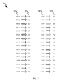
- An example of reducing binary values 152 from one group of three binary values to a ternary number represented as one group of two binary values that are provided as a output 199 to compaction enabled read controller and soft data output voltage value decoding circuit 180 is as follows:
- Corresponding SD Value Provided as SD Binary Values 152 Output 199 182 000 10 0.875 001 10 0.875 010 10 0.875 011 01 0.375 100 10 0.875 101 01 0.375 110 01 0.375 111 00 ⁇ 0.500
- Compaction enabled read controller and soft data output voltage value decoding circuit 180 converts the ternary number received as a group of two bits via output 199 into a corresponding soft data value that is provided as soft data 182 .
- Soft data 182 corresponding to the underlying LDPC codewords is provided low density parity check decoding circuit 190 .
- Low density parity check decoding circuit 190 applies a low density parity check decoding algorithm to soft data 182 to yield recovered read data 192 that is provided to host controller circuit 195 .
- compaction enabled read controller and soft data output voltage value decoding circuit 180 de-asserts compaction page indicator 197 to compaction based partial decoder circuit 198 .
- compaction based partial decoder circuit 198 Based upon the de-assertion of compaction page indicator 197 , compaction based partial decoder circuit 198 simply passes binary values 152 through to compaction enabled read controller and soft data output voltage value decoding circuit 180 unchanged as output 199 .
- Binary values 152 received as output 199 by compaction enabled read controller and soft data output voltage value decoding circuit 180 are decoded to yield soft data 182 corresponding to the underlying LDPC codewords (i.e., soft data representation of the originally encoded LDPC codewords 107 ).
- Soft data 182 corresponding to the underlying LDPC codewords is provided low density parity check decoding circuit 190 .
- Low density parity check decoding circuit 190 applies a low density parity check decoding algorithm to soft data 182 to yield recovered read data 192 that is provided to host controller circuit 195 .
- FIGS. 4 b -4 c the two approaches (compacted and non-compacted) for resolving binary values to yield soft data 182 to be processed by LDPC decoding circuit 190 based on either on non-compacted or compacted hard data depending upon which type of processing is selected.
- Compacted hard data processing may be selected to increase transfer efficiency.
- the non-compacted hard data processing generally results in reduced transfer efficiency.
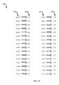
- FIG. 4 b a first part of the aforementioned process of comparing return voltages 142 with threshold 156 is shown in FIG. 4 b where the conversion of FIG. 4 a was used in the original encoding.
- This first part recovers a soft data representation of the first LDPC codeword (i.e., low density parity check codeword 201 ).
- a table 410 represents conversion of the three voltage levels 403 a , 403 b ( ⁇ X, Y, Z ⁇ ) of FIG. 4 a where threshold 156 is the lower threshold (V L ).
- any voltage value received as return voltages 142 that is less than V L results in a binary ‘0’
- any voltage value received as return voltages 142 that is greater than or equal to V L results in a binary ‘1’
- the corresponding binary output i.e., binary values 152
- the corresponding binary output is ‘110’ (shown as values 413 a , 413 b ).
- the corresponding binary output is ‘111’ (shown as values 413 a , 413 b ).
- These binary values map to a single soft data value corresponding to one LDPC codeword (i.e., low density parity check codeword 201 ).
- the three bit binary values 413 a , 413 b map to soft data for a corresponding five bit word (i.e., SD for XXXX 411 a , 411 b ).
- the conversion process may be done using a look up table that is loaded with pre-calculated soft data values corresponding to the respective three bit binary values.
- the soft data values corresponding to the respective three bit binary values may be calculated on the fly based upon the respective three bit binary values. Comparison of the next set of three cells of flash memory cells with V L is performed to yield the soft data value corresponding to the next bit of the LDPC codeword (i.e., low density parity check codeword 201 ). This process is repeated until soft data values corresponding to all bits of the LDPC codeword are generated (i.e., low density parity check codeword 201 ).
- the soft data values for any bit of a five bit word corresponding to the respective three bit binary values are calculated (either pre-calculated and stored to a look-up table, or calculated on the fly using a calculation circuit) in accordance with the following equation:
- Probability ⁇ ⁇ ( C , Y ) Probability ⁇ ⁇ ( Y
- C ′ ) , where Probability ⁇ ⁇ ( Y , C ) Probability ⁇ ⁇ ( Y
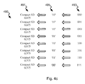
- FIG. 4 c an example of the first part of the aforementioned process of comparing return voltages 142 with threshold 156 are shown in FIG. 4 c where the conversion of FIG. 4 a was used in the original encoding.
- Such compaction based partial decoding increases transfer efficiency with the reduction corresponding to the amount of duplication in a soft data mapping table.
- FIG. 4 c one example shows the process of comparing return voltages 142 with a lower voltage threshold applied as threshold 156 to yield binary values 152 , and using a tree bit to two bit conversion where only three possible soft data values (0.875, 0.375, or ⁇ 0.500) for the first bit position (i.e., LDPC codeword 201 ).
- Compaction based partial decoder circuit 198 converts the three bits provided as binary values 152 into a ternary number (0, 1, 2) represented as a two bit compacted value shown in a column 495 .
- the two bit compacted value shown in column 495 is provided from compaction based partial decoder circuit 198 to compaction enabled read controller and soft data output voltage value decoding circuit 180 .
- Compaction enabled read controller and soft data output voltage value decoding circuit 180 generates a de-compacted soft data value shown in a column 497 corresponding to the received ternary number.
- the generated de-compacted soft data value is provided by compaction enabled read controller and soft data output voltage value decoding circuit 180 as soft data output 182 .
- the compaction goes from one group of three bits of binary values 152 into a single ternary number provided as output 199 resulting in a thirty-three percent data reduction.
- compaction based partial decoder circuit 198 may group three groups of bits of binary values 152 (i.e., a total of nine bits) into a five bit group representing three ternary numbers (i.e., three trits) representing twenty-seven possible combinations. Such compaction results in a forty-four percent data reduction.
- the five bit ternary number is provided as output 199 where it is converted into the three corresponding soft data values that are serially provided as soft data output 182 to LDPC decoding circuit 190 .
- compaction based partial decoder circuit 198 may group five groups of bits of binary values 152 (i.e., a total of fifteen bits) into an eight bit group representing five ternary numbers (i.e., five trits) representing two-hundred, forty-three possible combinations. Such compaction results in a fourty-seven percent data reduction.
- the eight bit ternary number is provided as output 199 where it is converted into the five corresponding soft data values that are serially provided as soft data output 182 to LDPC decoding circuit 190 .
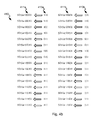
- FIG. 4 d a second part of the aforementioned process of comparing return voltages 142 with threshold 156 is shown where the conversion of FIG. 4 a was used in the original encoding.
- This second part recovers the second and third LDPC codewords (i.e., low density parity check codeword 203 and low density parity check codeword 205 ).
- a table 430 represents conversion of the three voltage levels 403 a , 403 b ( ⁇ X, Y, Z ⁇ ) of FIG. 4 a where threshold 156 is the center threshold (V C ).
- any voltage value received as return voltages 142 that is less than V C results in a binary ‘0’
- any voltage value received as return voltages 142 that is greater than or equal to V C results in a binary ‘1’
- the corresponding binary output i.e., binary values 152
- the corresponding binary output is ‘110’ (shown as values 433 a , 433 b ).
- the corresponding binary output is ‘101’ (shown as values 433 a , 433 b ).
- These binary values map to two soft data values corresponding to two LDPC codewords (i.e., low density parity check codeword 203 and low density parity check codeword 205 ).
- the three bit binary values 433 a , 433 b map to soft data for a corresponding five bit word (i.e., SD for XXXX 411 a , 411 b ).
- the conversion process may be done using a look up table that is loaded with pre-calculated soft data values corresponding to the respective three bit binary values.
- the soft data values corresponding to the respective three bit binary values may be calculated on the fly based upon the respective three bit binary values.
- the conversion may be done in accordance with the equations discussed above in relation to FIG. 4 b .
- Comparison of the next set of three cells of flash memory cells with V C is performed to yield the soft data values corresponding to the next bits of the two LDPC codewords (i.e., low density parity check codeword 203 and low density parity check codeword 205 ). This process is repeated until soft data values corresponding to all bits of the LDPC codewords are generated (i.e., low density parity check codeword 203 and low density parity check codeword 205 ).
- a ‘111’ pattern is an invalid value, but a soft data value is generated for it and all other valid patterns.
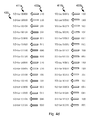
- FIG. 4 e a third part of the aforementioned process of comparing return voltages 142 with threshold 156 is shown where the conversion of FIG. 4 a was used in the original encoding.
- This third part recovers the fourth and fifth LDPC codewords (i.e., low density parity check codeword 207 and low density parity check codeword 209 ).
- a table 450 represents conversion of the three voltage levels 403 a , 403 b ( ⁇ X, Y, Z ⁇ ) of FIG. 4 a where threshold 156 is the upper threshold (V U ).
- any voltage value received as return voltages 142 that is less than V U results in a binary ‘0’
- any voltage value received as return voltages 142 that is greater than or equal to V U results in a binary ‘1’
- the corresponding binary output i.e., binary values 152
- the corresponding binary output is ‘000’ (shown as values 453 a , 453 b ).
- the corresponding binary output is ‘100’ (shown as values 453 a , 453 b ).
- These binary values map to two soft data values corresponding to two LDPC codewords (i.e., low density parity check codeword 203 and low density parity check codeword 205 ).
- the three bit binary values 453 a , 453 b map to soft data for a corresponding five bit word (i.e., SD for XXXX 411 a , 411 b ).
- the conversion process may be done using a look up table that is loaded with pre-calculated soft data values corresponding to the respective three bit binary values.
- the soft data values corresponding to the respective three bit binary values may be calculated on the fly based upon the respective three bit binary values.
- the conversion may be done in accordance with the equations discussed above in relation to FIG. 4 b .
- Comparison of the next set of three cells of flash memory cells with V U is performed to yield the soft data values corresponding to the next bits of the two LDPC codewords (i.e., low density parity check codeword 207 and low density parity check codeword 209 ). This process is repeated until soft data values corresponding to all bits of the LDPC codewords are generated (i.e., low density parity check codeword 207 and low density parity check codeword 209 ).
- a ‘111’ pattern is an invalid value, but a soft data value is generated for it and all other valid patterns.
- Solid state storage system 101 includes a compaction based partial decoder circuit 198 implemented on a semiconductor die 108 on which flash memory cells 140 are implemented in accordance with some embodiments of the present invention.
- Solid state storage system 101 includes a host controller circuit 195 , a low density parity check encoding circuit 105 , a voltage value encoding circuit 109 , a write circuit 130 , flash memory cells 140 , a buffering read circuit 150 , a compaction enabled read controller and soft data output voltage value decoding circuit 180 , and a low density parity check decoding circuit 190 .
- Host controller circuit 195 directs read and write access to flash memory cells 140 .
- Flash memory cells 140 may be NAND flash memory cells or another type of solid state memory cells as are known in the art.
- Solid state storage system 101 is implemented using at least two distinct semiconductor dies.
- Semiconductor die 106 includes low density parity check encoding circuit 105 , voltage value encoding circuit 109 , compaction enabled read controller and soft data output voltage value decoding circuit 180 , and low density parity check decoding circuit 190 .
- Semiconductor die 108 includes write circuit 130 , compaction based partial decoder circuit 198 flash memory cells 140 , and buffering read circuit 150 .
- solid state storage system 101 is shown as distributed across two or more semiconductor dies, that other embodiments of the present invention may be implemented with a semiconductor die that includes all of low density parity check encoding circuit 105 , voltage value encoding circuit 109 , write circuit 130 , flash memory cells 140 , buffering read circuit 150 , compaction enabled read controller and soft data output voltage value decoding circuit 180 , and low density parity check decoding circuit 190 .
- Yet other embodiments of the present invention may be implemented with a semiconductor die that includes all of low density parity check encoding circuit 105 , voltage value encoding circuit 109 , write circuit 130 , flash memory cells 140 , buffering read circuit 150 , compaction enabled read controller and soft data output voltage value decoding circuit 180 , low density parity check decoding circuit 190 , and host controller circuit 195 .
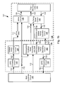
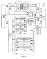
- Solid state storage system 500 includes a compaction based partial decoder circuit 598 in accordance with some embodiments of the present invention.
- Solid state storage system 500 includes a host controller circuit 595 , a low density parity check encoding circuit 505 , a voltage value encoding circuit 509 shown in dashed lines, a write circuit 530 , flash memory cells 540 , a read circuit 550 , compaction based partial decoder circuit 598 , a compaction enabled read controller and soft data output voltage value decoding circuit 580 shown in dashed lines, and a low density parity check decoding circuit 590 .
- Compaction enabled read controller and soft data output voltage value decoding circuit 580 includes a read controller circuit 570 , a serial to parallel buffer circuit 560 , and three non-compacted page soft data output decoding circuits 574 , 576 , 578 , and three compacted page soft data output decoding circuits 1574 , 1576 , 1578 .
- Voltage value encoding circuit 509 includes a multiple codeword buffer circuit 511 and a multi-level cell encoder circuit 515 .
- Host controller circuit 595 directs read and write access to flash memory cells 540 . Flash memory cells 540 may be NAND flash memory cells or another type of solid state memory cells as are known in the art.
- a data write is effectuated when host controller circuit 595 provides input data 503 to low density parity check encoding circuit 505 .
- Low density parity check encoding circuit 505 applies a low density parity check encoding algorithm to input data 503 to yield LDPC codewords 507 .
- Low density parity check encoding circuit 505 may be any circuit known in the art that is capable of receiving user data and generating corresponding low density parity check codewords.
- LDPC codewords 507 are provided to multi-level cell encoding circuit 509 .
- Multiple codeword buffer circuit 511 of voltage value encoding circuit 509 stores five LDPC codewords received as LDPC codewords 507 .
- Voltage value 517 corresponds to a voltage level that is to be written to a first of a three cell block of flash memory cells 540
- voltage value 519 corresponds to a voltage level that is to be written to a second of the three cell block of flash memory cells 140
- voltage value 521 corresponds to a voltage level that is to be written to a third of the three cell block of flash memory cells 540
- voltage values 517 , 519 , 521 may be one of four voltage levels each representing a two-bit pattern stored in a given cell of flash memory cells 540 . It should be noted that in other embodiments, eight or more voltage levels representing three or more bits stored in a given cell of flash memory cells 540 are possible in accordance with other embodiments of the present invention.
- multi-level cell encoding 200 is shown using multiple low density parity check codewords 201 , 203 , 205 , 207 , 209 to yield a series of five bit words 513 that are encoded into write data in accordance with some embodiments of the present invention.
- Each of the low density parity check codewords 201 , 203 , 205 , 207 , 209 includes a number of bits indicated as positions (i.e., position 1 , position 2 , . . . position n ⁇ 1, and position n).
- a five bit word 513 includes the first element of each of the five low density parity check codewords 201 , 203 , 205 , 207 , 209 (i.e., ⁇ A 1 , B 1 , C 1 , D 1 , E 1 ⁇ ). This is repeated for each of the positions 1 through n to yield n five bit words 513 (i.e., ⁇ A 2 , B 2 , C 2 , D 2 , E 2 ⁇ . . . ⁇ A n , B n , C n , D n , E n ⁇ ).
- multi-level cell encoder circuit 515 encodes each of the n five bit words 513 to a corresponding three value output that is provided as voltage values 517 , 519 , 521 to write circuit 530 .
- a five bit word 301 a , 301 b ( ⁇ A, B, C, D, E ⁇ ) to three voltage levels 303 a , 303 b ( ⁇ X, Y, Z ⁇ ) conversion table 300 is shown in accordance with some embodiments of the present invention.
- five bit word 301 a , 301 b correspond to the five bit words ( ⁇ A, B, C, D, E ⁇ ) discussed above in relation to FIG. 2 .
- FIG. 4 a another five bit word 401 a , 401 b ( ⁇ A, B, C, D, E ⁇ ) to three voltage levels 403 a , 403 b ( ⁇ X, Y, Z ⁇ ) conversion table 400 in accordance with some embodiments of the present invention.
- five bit word 401 a , 401 b correspond to the five bit words ( ⁇ A, B, C, D, E ⁇ ) discussed above in relation to FIG. 2 .
- the corresponding three voltage levels are “2, 2, 0”.
- three voltage levels are “3, 1, 2”
- the corresponding five bit word is ‘10101’.
- the aforementioned conversion tables are from five bit words to three voltage levels, other conversions may be possible in accordance with various embodiments of the present invention.
- other embodiments of the present invention may use conversion tables from four bit words to three voltage levels. Based upon the disclosure provided herein, one of ordinary skill in the art will recognize other conversion tables that may be used in accordance with various embodiments of the present invention.
- write circuit 530 additionally receives an address 510 from host controller circuit 595 .
- Write circuit 530 converts voltage values 517 , 519 , 521 (e.g., ⁇ X, Y, Z ⁇ ) into a series of voltages 535 that are written to three cells of flash memory cells 540 indicated by address 510 .
- a voltage level of “0” results in voltage 535 being set below a lower threshold (V L )
- a voltage level of “1” results in voltage 535 being set above the lower threshold (V L ) and below a center threshold (V C )
- a voltage level of “2” results in voltage 535 being set above the center threshold (V C ) and below an upper threshold (V U )
- a voltage level of “3” results in voltage 535 being set above the upper threshold (V U ).
- This process results in storing three voltage values respectively to three cells within flash memory cells to represent a five bit word. This process is repeated for each of the five bit words resulting in a group of multiple sets of three flash memory cells representing the five LDPC codewords received as LDPC codewords 507 .
- a data read is effectuated when host controller circuit 595 provides a read request indication 512 and address 510 to read controller circuit 570 of compaction enabled read controller and soft data output voltage value decoding circuit 580 .
- Read controller circuit 570 translates read request 512 and address 510 into an address 554 and a threshold value 556 (or series of threshold values) that are provided to read circuit 550 .
- a read location 544 is generated by read circuit 550 based upon address 554 and provided to flash memory cells 540 .
- flash memory cells 540 provides return voltages 542 stored at the cells indicated by read location 544 .
- Read circuit 550 compares return voltages 542 with threshold 556 to yield corresponding binary values 552 .
- Binary values 552 are provided to serial to parallel buffer 560 that assembles the binary values into sets of three bits 562 , 564 , 566 associated with the same five bit words. Bits 562 , 564 , 566 are provided to each of page 0 soft data output decoding circuit 574 , page 1 soft data output decoding circuit 576 , and page 2 soft data output decoding circuit 578 . Based upon the ongoing read, read controller circuit 570 asserts various enables 572 that enable operation of respective ones of page 0 soft data output decoding circuit 574 , page 1 soft data output decoding circuit 576 , and page 2 soft data output decoding circuit 578 .
- read controller circuit 570 sequentially provides: the lower threshold (V L ) to obtain the soft data corresponding to the first LDPC codeword represented in the five bit words, the center threshold (V C ) to obtain the soft data corresponding to the second and third LDPC codewords represented in the five bit words, and the upper threshold (V U ) to obtain the soft data corresponding to the fourth and fifth LDPC codewords represented in the five bit words as threshold value 556 .
- some subset of the lower threshold (V L ), the center threshold (V C ), and/or the upper threshold (V U ) are sequentially presented as threshold value 556 .
- the center threshold (V C ), and/or the upper threshold (V U ) are sequentially presented as threshold value 556 .
- the upper threshold (V U ) is presented.
- V L threshold
- enables 572 are asserted by read controller circuit 570 such that operation of page 0 soft data output decoding circuit 574 is enabled, while operation of page 1 soft data output decoding circuit 576 and page 2 soft data output decoding circuit 578 is disabled.
- page 0 soft data output decoding circuit 574 When enabled, page 0 soft data output decoding circuit 574 generates soft data corresponding to the first LDPC codeword represented in the five bit words based upon bits 562 , 564 , 566 corresponding to the result of comparing return voltages 542 with the lower threshold (V L ). The generated soft data corresponding to the first LDPC codeword is provided as a soft data output 582 to LDPC decoding circuit 590 .
- page 1 soft data output decoding circuit 576 when enabled, page 1 soft data output decoding circuit 576 generates soft data corresponding to the second and third LDPC codewords represented in the five bit words based upon bits 562 , 564 , 566 corresponding to the result of comparing return voltages 542 with the center threshold (V C ).
- the generated soft data corresponding to the second and third LDPC codewords is provided as a soft data output 584 to LDPC decoding circuit 590 .
- page 2 soft data output decoding circuit 578 when enabled, page 2 soft data output decoding circuit 578 generates soft data corresponding to the fourth and fifth LDPC codewords represented in the five bit words based upon bits 562 , 564 , 566 corresponding to the result of comparing return voltages 542 with the upper threshold (V U ).
- the generated soft data corresponding to the fourth and fifth LDPC codewords is provided as a soft data output 586 to LDPC decoding circuit 590 .
- binary values 552 are provided to compaction based partial decoder circuit 598 that compacts the binary values 552 into corresponding ternary numbers that are provided via a multi-line interface 1564 , 1566 to compacted page soft data output decoding circuits 1574 , 1576 , 1578 .
- compaction based partial decoder circuit 598 reduces binary values 552 from one or more groups of three binary values to a ternary number represented as a group of two binary values that are provided as a output 599 to compaction enabled read controller and soft data output voltage value decoding circuit 580 .
- An example of reducing binary values 552 from one group of three binary values to a ternary number represented as one group of two binary values that are provided as a output 599 to compaction enabled read controller and soft data output voltage value decoding circuit 580 is as follows:
- Compaction enabled read controller and soft data output voltage value decoding circuit 580 converts the ternary number received as multi-line interface 1564 , 1566 into a corresponding soft data value that is provided to LDPC decoding circuit 590 .
- page 0 compacted soft data output decoding circuit 1574 generates one or more soft data values corresponding to the ternary number received via multi-line interface 1564 , 1566 .
- the generated soft data is provided as a soft data output 1582 when page 0 is enabled by enables 572 .
- page 0 compacted soft data output decoding circuit 1574 is a look-up table.
- page 0 compacted soft data output decoding circuit 1574 is a non-table based data conversion circuit.
- page 1 compacted soft data output decoding circuit 1576 generates one or more soft data values corresponding to the ternary number received via multi-line interface 1564 , 1566 .
- the generated soft data is provided as a soft data output 1584 when page 1 is enabled by enables 572 .
- page 1 compacted soft data output decoding circuit 1576 is a look-up table.
- page 1 compacted soft data output decoding circuit 1576 is a non-table based data conversion circuit.
- page 2 compacted soft data output decoding circuit 1578 generates one or more soft data values corresponding to the ternary number received via multi-line interface 1564 , 1566 .
- the generated soft data is provided as a soft data output 1586 when page 2 is enabled by enables 572 .
- page 2 compacted soft data output decoding circuit 1578 is a look-up table.
- page 2 compacted soft data output decoding circuit 1578 is a non-table based data conversion circuit.
- solid state storage system 500 is shown as including both compacted and non-compacted decoding circuitry for all pages allowing for a wide range of selecting combinations of compacted and/or non-compacted operations on a page by page basis, other embodiments may include less circuitry. For example, one embodiment may only include compacted decoding circuitry for each of the pages (i.e., serial to parallel buffer 560 , page 0 soft output decoding circuit 574 , page 1 soft output decoding circuit 576 , and page 2 soft output decoding circuit 578 are eliminated).
- another embodiment may include only compacted decoding circuitry for page 0 and only non-compacted decoding circuitry for page 1 and page 2 (i.e., page 0 soft output decoding circuit 574 , page 1 compacted soft output decoding circuit 1576 , and page 2 compacted soft output decoding circuit 1578 are eliminated).
- page 0 soft output decoding circuit 574 page 1 compacted soft output decoding circuit 1576
- page 2 compacted soft output decoding circuit 1578 are eliminated.
- FIGS. 4 b -4 c the two approaches (compacted and non-compacted) for resolving binary values to yield the soft data to be processed by LDPC decoding circuit 590 based on either on non-compacted or compacted hard data depending upon which type of processing is selected.
- Compacted hard data processing may be selected to increase transfer efficiency.
- the non-compacted hard data processing generally results in reduced transfer efficiency.
- FIG. 4 b a first part of the aforementioned process of comparing return voltages 542 with threshold 556 is shown in FIG. 4 b where the conversion of FIG. 4 a was used in the original encoding.
- This first part recovers a soft data representation of the first LDPC codeword (i.e., low density parity check codeword 201 ).
- a table 410 represents conversion of the three voltage levels 403 a , 403 b ( ⁇ X, Y, Z ⁇ ) of FIG. 4 a where threshold 556 is the lower threshold (V L ).
- any voltage value received as return voltages 542 that is less than V L results in a binary ‘0’
- any voltage value received as return voltages 542 that is greater than or equal to V L results in a binary ‘1’
- the corresponding binary output i.e., binary values 552
- the corresponding binary output is ‘110’ (shown as values 413 a , 413 b ).
- the corresponding binary output is ‘111’ (shown as values 413 a , 413 b ).
- These binary values map to a single soft data value corresponding to one LDPC codeword (i.e., low density parity check codeword 201 ).
- the three bit binary values 413 a , 413 b map to soft data for a corresponding five bit word (i.e., SD for XXXX 411 a , 411 b ).
- the conversion process may be done using a look up table that is loaded with pre-calculated soft data values corresponding to the respective three bit binary values.
- the soft data values corresponding to the respective three bit binary values may be calculated on the fly based upon the respective three bit binary values. Comparison of the next set of three cells of flash memory cells with V L is performed to yield the soft data value corresponding to the next bit of the LDPC codeword (i.e., low density parity check codeword 201 ). This process is repeated until soft data values corresponding to all bits of the LDPC codeword are generated (i.e., low density parity check codeword 201 ).
- the soft data values for any bit of a five bit word corresponding to the respective three bit binary values are calculated (either pre-calculated and stored to a look-up table, or calculated on the fly using a calculation circuit) in accordance with the following equation:
- Probability ⁇ ⁇ ( C , Y ) Probability ⁇ ⁇ ( Y
- C ′ ) , where Probability ⁇ ⁇ ( Y , C ) Probability ⁇ ⁇ ( Y
- FIG. 4 c an example of the first part of the aforementioned process of comparing return voltages 542 with threshold 556 are shown in FIG. 4 c where the conversion of FIG. 4 a was used in the original encoding.
- Such compaction based partial decoding increases transfer efficiency with the reduction corresponding to the amount of duplication in a soft data mapping table.
- FIG. 4 c one example shows the process of comparing return voltages 542 with a lower voltage threshold applied as threshold 556 to yield binary values 552 , and using a tree bit to two bit conversion where only three possible soft data values (0.875, 0.375, or ⁇ 0.500) for the first bit position (i.e., LDPC codeword 201 ).
- Compaction based partial decoder circuit 598 converts the three bits provided as binary values 552 into a ternary number (0, 1, 2) represented as a two bit value shown in a column 495 .
- the two bit value shown in column 495 is provided from compaction based partial decoder circuit 598 to compaction enabled read controller and soft data output voltage value decoding circuit 580 .
- Compaction enabled read controller and soft data output voltage value decoding circuit 580 generates a soft data value shown in a column 497 corresponding to the received ternary number.
- the generated soft data value is provided by compaction enabled read controller and soft data output voltage value decoding circuit 580 as soft data output 582 .
- the compaction goes from one group of three bits of binary values 552 into a single ternary number (which can be represented by two bits) provided as output 599 resulting in a thirty-three percent data reduction.
- compaction based partial decoder circuit 598 may group three groups of bits of binary values 552 (i.e., a total of nine bits) into into a five bit group representing three ternary numbers (i.e., three trits) representing twenty-seven possible combinations. Such compaction results in a forty-four percent data reduction.
- the five bit ternary number is provided as output 599 where it is converted into the three corresponding soft data values that are serially provided as soft data output 582 to LDPC decoding circuit 590 .
- compaction based partial decoder circuit 598 may group five groups of bits of binary values 552 (i.e., a total of fifteen bits) into an eight bit group representing five ternary numbers (i.e., five trits) representing two-hundred, forty-three possible combinations. Such compaction results in a fourty-seven percent data reduction.
- the eight bit ternary number is provided as output 599 where it is converted into the five corresponding soft data values that are serially provided as soft data output 582 to LDPC decoding circuit 590 .
- FIG. 4 d a second part of the aforementioned process of comparing return voltages 542 with threshold 556 is shown where the conversion of FIG. 4 a was used in the original encoding.
- This second part recovers the second and third LDPC codewords (i.e., low density parity check codeword 203 and low density parity check codeword 205 ).
- a table 430 represents conversion of the three voltage levels 403 a , 403 b ( ⁇ X, Y, Z ⁇ ) of FIG. 4 a where threshold 556 is the center threshold (V C ).
- any voltage value received as return voltages 542 that is less than V C results in a binary ‘0’
- any voltage value received as return voltages 542 that is greater than or equal to V C results in a binary ‘1’
- the corresponding binary output i.e., binary values 552
- the corresponding binary output is ‘110’ (shown as values 433 a , 433 b ).
- the corresponding binary output is ‘101’ (shown as values 433 a , 433 b ).
- These binary values map to two soft data values corresponding to two LDPC codewords (i.e., low density parity check codeword 203 and low density parity check codeword 205 ).
- the three bit binary values 433 a , 433 b map to soft data for a corresponding five bit word (i.e., SD for XXXX 411 a , 411 b ).
- the conversion process may be done using a look up table that is loaded with pre-calculated soft data values corresponding to the respective three bit binary values.
- the soft data values corresponding to the respective three bit binary values may be calculated on the fly based upon the respective three bit binary values.
- the conversion may be done in accordance with the equations discussed above in relation to FIG. 4 b .
- Comparison of the next set of three cells of flash memory cells with V C is performed to yield the soft data values corresponding to the next bits of the two LDPC codewords (i.e., low density parity check codeword 203 and low density parity check codeword 205 ). This process is repeated until soft data values corresponding to all bits of the LDPC codewords are generated (i.e., low density parity check codeword 203 and low density parity check codeword 205 ).
- a ‘111’ pattern is an invalid value, but a soft data value is generated for it and all other valid patterns.
- FIG. 4 e a third part of the aforementioned process of comparing return voltages 542 with threshold 556 is shown where the conversion of FIG. 4 a was used in the original encoding.
- This third part recovers the fourth and fifth LDPC codewords (i.e., low density parity check codeword 207 and low density parity check codeword 209 ).
- a table 450 represents conversion of the three voltage levels 403 a , 403 b ( ⁇ X, Y, Z ⁇ ) of FIG. 4 a where threshold 556 is the upper threshold (V U ).
- any voltage value received as return voltages 542 that is less than V U results in a binary ‘0’
- any voltage value received as return voltages 542 that is greater than or equal to V U results in a binary ‘1’
- the corresponding binary output i.e., binary values 552
- the corresponding binary output is ‘000’ (shown as values 453 a , 453 b ).
- the corresponding binary output is ‘100’ (shown as values 453 a , 453 b ).
- These binary values map to two soft data values corresponding to two LDPC codewords (i.e., low density parity check codeword 203 and low density parity check codeword 205 ).
- the three bit binary values 453 a , 453 b map to soft data for a corresponding five bit word (i.e., SD for XXXX 411 a , 411 b ).
- the conversion process may be done using a look up table that is loaded with pre-calculated soft data values corresponding to the respective three bit binary values.
- the soft data values corresponding to the respective three bit binary values may be calculated on the fly based upon the respective three bit binary values.
- the conversion may be done in accordance with the equations discussed above in relation to FIG. 4 b .
- Comparison of the next set of three cells of flash memory cells with V U is performed to yield the soft data values corresponding to the next bits of the two LDPC codewords (i.e., low density parity check codeword 207 and low density parity check codeword 209 ). This process is repeated until soft data values corresponding to all bits of the LDPC codewords are generated (i.e., low density parity check codeword 207 and low density parity check codeword 209 ).
- a ‘111’ pattern is an invalid value, but a soft data value is generated for it and all other valid patterns.
- Such integrated circuits may include all of the functions of a given block, system or circuit, or a subset of the block, system or circuit. Further, elements of the blocks, systems or circuits may be implemented across multiple integrated circuits. Such integrated circuits may be any type of integrated circuit known in the art including, but are not limited to, a monolithic integrated circuit, a flip chip integrated circuit, a multichip module integrated circuit, and/or a mixed signal integrated circuit. It should also be noted that various functions of the blocks, systems or circuits discussed herein may be implemented in either software or firmware.
- the entire system, block or circuit may be implemented using its software or firmware equivalent—albeit such a system entirely implemented in software or firmware would not be a circuit.
- the one part of a given system, block or circuit may be implemented in software or firmware, while other parts are implemented in hardware.
Landscapes
- Engineering & Computer Science (AREA)
- Theoretical Computer Science (AREA)
- Physics & Mathematics (AREA)
- Probability & Statistics with Applications (AREA)
- Quality & Reliability (AREA)
- General Engineering & Computer Science (AREA)
- General Physics & Mathematics (AREA)
- Read Only Memory (AREA)
Abstract
Description
| Corresponding | ||
| SD Value | ||
| Provided as | ||
| Binary Values | ||
| 152 | | 182 |
| 000 | 10 | 0.875 |
| 001 | 10 | 0.875 |
| 010 | 10 | 0.875 |
| 011 | 01 | 0.375 |
| 100 | 10 | 0.875 |
| 101 | 01 | 0.375 |
| 110 | 01 | 0.375 |
| 111 | 00 | −0.500 |
Compaction enabled read controller and soft data output voltage
where LLR is a log-likelihood ratio, Y represents the three
where C are the three voltages provided from flash memory cells; where:
for the case of additive white Gaussian noise:
In various cases, quantized inputs are used in place of the three bit binary values. In such a case, the soft data output corresponding to the quantized inputs is calculated in accordance with the following equation:
where U represents a quantized version of the three
| Binary | Multi-line | |
| Values | Interface | Corresponding |
| 552 | 1564, 1566 | |
| 000 | 10 | 0.875 |
| 001 | 10 | 0.875 |
| 010 | 10 | 0.875 |
| 011 | 01 | 0.375 |
| 100 | 10 | 0.875 |
| 101 | 01 | 0.375 |
| 110 | 01 | 0.375 |
| 111 | 00 | −0.500 |
Compaction enabled read controller and soft data output voltage
where LLR is a log-likelihood ratio, Y represents the three
where C are the three voltages provided from flash memory cells; where:
for the case of additive white Gaussian noise:
In various cases, quantized inputs are used in place of the three bit binary values. In such a case, the soft data output corresponding to the quantized inputs is calculated in accordance with the following equation:
where U represents a quantized version of the three
Claims (20)
Priority Applications (1)
| Application Number | Priority Date | Filing Date | Title |
|---|---|---|---|
| US14/925,726 US9740559B2 (en) | 2015-10-28 | 2015-10-28 | Systems and methods for compaction based flash memory data recovery |
Applications Claiming Priority (1)
| Application Number | Priority Date | Filing Date | Title |
|---|---|---|---|
| US14/925,726 US9740559B2 (en) | 2015-10-28 | 2015-10-28 | Systems and methods for compaction based flash memory data recovery |
Publications (2)
| Publication Number | Publication Date |
|---|---|
| US20170123900A1 US20170123900A1 (en) | 2017-05-04 |
| US9740559B2 true US9740559B2 (en) | 2017-08-22 |
Family
ID=58634701
Family Applications (1)
| Application Number | Title | Priority Date | Filing Date |
|---|---|---|---|
| US14/925,726 Active 2036-02-16 US9740559B2 (en) | 2015-10-28 | 2015-10-28 | Systems and methods for compaction based flash memory data recovery |
Country Status (1)
| Country | Link |
|---|---|
| US (1) | US9740559B2 (en) |
Cited By (1)
| Publication number | Priority date | Publication date | Assignee | Title |
|---|---|---|---|---|
| US11206046B2 (en) | 2019-08-13 | 2021-12-21 | Samsung Electronics Co., Ltd. | Operating method of memory controller, storage device and the operating method thereof |
Families Citing this family (8)
| Publication number | Priority date | Publication date | Assignee | Title |
|---|---|---|---|---|
| US9886342B2 (en) | 2015-10-28 | 2018-02-06 | Sandisk Technologies Llc | Storage device operations based on bit error rate (BER) estimate |
| US10180874B2 (en) | 2015-10-28 | 2019-01-15 | Western Digital Technologies, Inc. | Storage device operations based on bit error rate (BER) estimate |
| US10204006B2 (en) * | 2015-10-28 | 2019-02-12 | Avago Technologies International Sales Pte. Limited | Systems and methods for side data based soft data flash memory access |
| US10198316B2 (en) * | 2015-10-28 | 2019-02-05 | Avago Technologies International Sales Pte. Limited | Systems and methods for efficient flash memory access |
| US10108489B2 (en) * | 2015-10-28 | 2018-10-23 | Avago Technologies General Ip (Singapore) Pte. Ltd. | Systems and methods for efficient soft data based flash memory data recovery |
| US9978462B2 (en) * | 2015-10-29 | 2018-05-22 | Sandisk Technologies Llc | Partial soft bit read |
| US20180062887A1 (en) * | 2016-08-24 | 2018-03-01 | Qualcomm Incorporated | Using full ternary transcoding in i3c high data rate mode |
| US11546000B2 (en) * | 2020-05-04 | 2023-01-03 | Samsung Electronics Co., Ltd. | Mobile data storage |
Citations (13)
| Publication number | Priority date | Publication date | Assignee | Title |
|---|---|---|---|---|
| US20080288849A1 (en) * | 2007-05-17 | 2008-11-20 | Samsung Electronics Co., Ltd | Apparatus for generating soft decision values and method thereof |
| US20090248952A1 (en) * | 2008-03-31 | 2009-10-01 | Radke William H | Data conditioning to improve flash memory reliability |
| US20110167305A1 (en) * | 2008-09-30 | 2011-07-07 | Haratsch Erich F | Methods and Apparatus for Soft Data Generation for Memory Devices Based on Performance Factor Adjustment |
| US20110246855A1 (en) * | 2010-04-02 | 2011-10-06 | Skymedi Corporation | Method and Apparatus of Generating a Soft Value for a Memory Device |
| US8065583B2 (en) | 2007-07-06 | 2011-11-22 | Micron Technology, Inc. | Data storage with an outer block code and a stream-based inner code |
| US20120079351A1 (en) * | 2010-09-24 | 2012-03-29 | International Business Machines Corporation | Systems and Methods for Memory Devices |
| US20130073798A1 (en) | 2011-09-20 | 2013-03-21 | Samsung Electronics Co., Ltd. | Flash memory device and data management method |
| US8947929B1 (en) * | 2008-11-06 | 2015-02-03 | Marvell International Ltd. | Flash-based soft information generation |
| US9214965B2 (en) * | 2013-02-20 | 2015-12-15 | Sandisk Enterprise Ip Llc | Method and system for improving data integrity in non-volatile storage |
| US9286155B1 (en) * | 2013-05-24 | 2016-03-15 | Marvell International Ltd. | Systems and methods for generating soft information in a flash device |
| US20160218740A1 (en) * | 2015-01-28 | 2016-07-28 | Micron Technology, Inc. | Estimating an error rate associated with memory |
| US9450610B1 (en) * | 2013-03-15 | 2016-09-20 | Microsemi Storage Solutions (Us), Inc. | High quality log likelihood ratios determined using two-index look-up table |
| US20170046220A1 (en) * | 2015-08-11 | 2017-02-16 | Sandisk Technologies Inc. | Soft bit techniques for a data storage device |
-
2015
- 2015-10-28 US US14/925,726 patent/US9740559B2/en active Active
Patent Citations (13)
| Publication number | Priority date | Publication date | Assignee | Title |
|---|---|---|---|---|
| US20080288849A1 (en) * | 2007-05-17 | 2008-11-20 | Samsung Electronics Co., Ltd | Apparatus for generating soft decision values and method thereof |
| US8065583B2 (en) | 2007-07-06 | 2011-11-22 | Micron Technology, Inc. | Data storage with an outer block code and a stream-based inner code |
| US20090248952A1 (en) * | 2008-03-31 | 2009-10-01 | Radke William H | Data conditioning to improve flash memory reliability |
| US20110167305A1 (en) * | 2008-09-30 | 2011-07-07 | Haratsch Erich F | Methods and Apparatus for Soft Data Generation for Memory Devices Based on Performance Factor Adjustment |
| US8947929B1 (en) * | 2008-11-06 | 2015-02-03 | Marvell International Ltd. | Flash-based soft information generation |
| US20110246855A1 (en) * | 2010-04-02 | 2011-10-06 | Skymedi Corporation | Method and Apparatus of Generating a Soft Value for a Memory Device |
| US20120079351A1 (en) * | 2010-09-24 | 2012-03-29 | International Business Machines Corporation | Systems and Methods for Memory Devices |
| US20130073798A1 (en) | 2011-09-20 | 2013-03-21 | Samsung Electronics Co., Ltd. | Flash memory device and data management method |
| US9214965B2 (en) * | 2013-02-20 | 2015-12-15 | Sandisk Enterprise Ip Llc | Method and system for improving data integrity in non-volatile storage |
| US9450610B1 (en) * | 2013-03-15 | 2016-09-20 | Microsemi Storage Solutions (Us), Inc. | High quality log likelihood ratios determined using two-index look-up table |
| US9286155B1 (en) * | 2013-05-24 | 2016-03-15 | Marvell International Ltd. | Systems and methods for generating soft information in a flash device |
| US20160218740A1 (en) * | 2015-01-28 | 2016-07-28 | Micron Technology, Inc. | Estimating an error rate associated with memory |
| US20170046220A1 (en) * | 2015-08-11 | 2017-02-16 | Sandisk Technologies Inc. | Soft bit techniques for a data storage device |
Cited By (1)
| Publication number | Priority date | Publication date | Assignee | Title |
|---|---|---|---|---|
| US11206046B2 (en) | 2019-08-13 | 2021-12-21 | Samsung Electronics Co., Ltd. | Operating method of memory controller, storage device and the operating method thereof |
Also Published As
| Publication number | Publication date |
|---|---|
| US20170123900A1 (en) | 2017-05-04 |
Similar Documents
| Publication | Publication Date | Title |
|---|---|---|
| US9740559B2 (en) | Systems and methods for compaction based flash memory data recovery | |
| US10204006B2 (en) | Systems and methods for side data based soft data flash memory access | |
| CN101645295B (en) | Accessing memory using fractional reference voltages | |
| US8830746B2 (en) | Optimized threshold search in analog memory cells using separator pages of the same type as read pages | |
| JP5620973B2 (en) | Search for optimum threshold in analog memory cells | |
| JP5621175B2 (en) | Method and apparatus for inter-cell interference mitigation using modulation coding | |
| US8869008B2 (en) | Adaptation of analog memory cell read thresholds using partial ECC syndromes | |
| US10108489B2 (en) | Systems and methods for efficient soft data based flash memory data recovery | |
| DE112011101116B4 (en) | Two-level BCH codes for solid-state storage devices | |
| US20140181617A1 (en) | Management of non-valid decision patterns of a soft read retry operation | |
| US9984752B2 (en) | Memory system and data encoding and decoding method to mitigate inter-cell interference | |
| US10298264B2 (en) | Systems and methods for soft decision generation in a solid state memory system | |
| US20170093427A1 (en) | Systems and methods for soft data utilization in a solid state memory system | |
| US10326473B2 (en) | Symbol-based coding for NAND flash devices | |
| KR100272153B1 (en) | 3 value memory system | |
| US9450619B2 (en) | Dynamic log likelihood ratio quantization for solid state drive controllers | |
| US10198316B2 (en) | Systems and methods for efficient flash memory access | |
| KR102007163B1 (en) | Encoder, decoder and semiconductor device including the same | |
| US20230308208A1 (en) | High throughput polar ecc decoding via compressed successive cancellation algorithm | |
| JP4212594B2 (en) | Multilevel semiconductor memory device, writing method thereof, and storage medium | |
| US9172399B2 (en) | Updating variable nodes associated with an iterative decoder | |
| US20190089377A1 (en) | Memory system and method of controlling nonvolatile memory |
Legal Events
| Date | Code | Title | Description |
|---|---|---|---|
| AS | Assignment |
Owner name: AVAGO TECHNOLOGIES IP (SINGAPORE) PTE. LTD., SINGA Free format text: ASSIGNMENT OF ASSIGNORS INTEREST;ASSIGNOR:ZHAO, ZHIJUN;REEL/FRAME:036906/0283 Effective date: 20151027 |
|
| AS | Assignment |
Owner name: BANK OF AMERICA, N.A., AS COLLATERAL AGENT, NORTH Free format text: PATENT SECURITY AGREEMENT;ASSIGNOR:AVAGO TECHNOLOGIES GENERAL IP (SINGAPORE) PTE. LTD.;REEL/FRAME:037808/0001 Effective date: 20160201 Owner name: BANK OF AMERICA, N.A., AS COLLATERAL AGENT, NORTH CAROLINA Free format text: PATENT SECURITY AGREEMENT;ASSIGNOR:AVAGO TECHNOLOGIES GENERAL IP (SINGAPORE) PTE. LTD.;REEL/FRAME:037808/0001 Effective date: 20160201 |
|
| AS | Assignment |
Owner name: AVAGO TECHNOLOGIES GENERAL IP (SINGAPORE) PTE. LTD Free format text: ASSIGNMENT OF ASSIGNORS INTEREST;ASSIGNOR:ZHAO, ZHIJUN;REEL/FRAME:037804/0141 Effective date: 20151027 |
|
| AS | Assignment |
Owner name: AVAGO TECHNOLOGIES GENERAL IP (SINGAPORE) PTE. LTD Free format text: TERMINATION AND RELEASE OF SECURITY INTEREST IN PATENTS;ASSIGNOR:BANK OF AMERICA, N.A., AS COLLATERAL AGENT;REEL/FRAME:041710/0001 Effective date: 20170119 Owner name: AVAGO TECHNOLOGIES GENERAL IP (SINGAPORE) PTE. LTD., SINGAPORE Free format text: TERMINATION AND RELEASE OF SECURITY INTEREST IN PATENTS;ASSIGNOR:BANK OF AMERICA, N.A., AS COLLATERAL AGENT;REEL/FRAME:041710/0001 Effective date: 20170119 |
|
| STCF | Information on status: patent grant |
Free format text: PATENTED CASE |
|
| AS | Assignment |
Owner name: AVAGO TECHNOLOGIES INTERNATIONAL SALES PTE. LIMITE Free format text: MERGER;ASSIGNOR:AVAGO TECHNOLOGIES GENERAL IP (SINGAPORE) PTE. LTD.;REEL/FRAME:047422/0464 Effective date: 20180509 |
|
| AS | Assignment |
Owner name: AVAGO TECHNOLOGIES INTERNATIONAL SALES PTE. LIMITE Free format text: CORRECTIVE ASSIGNMENT TO CORRECT THE EXECUTION DATE PREVIOUSLY RECORDED AT REEL: 047422 FRAME: 0464. ASSIGNOR(S) HEREBY CONFIRMS THE MERGER;ASSIGNOR:AVAGO TECHNOLOGIES GENERAL IP (SINGAPORE) PTE. LTD.;REEL/FRAME:048883/0702 Effective date: 20180905 |
|
| AS | Assignment |
Owner name: BROADCOM INTERNATIONAL PTE. LTD., SINGAPORE Free format text: ASSIGNMENT OF ASSIGNORS INTEREST;ASSIGNOR:AVAGO TECHNOLOGIES INTERNATIONAL SALES PTE. LIMITED;REEL/FRAME:053771/0901 Effective date: 20200826 |
|
| MAFP | Maintenance fee payment |
Free format text: PAYMENT OF MAINTENANCE FEE, 4TH YEAR, LARGE ENTITY (ORIGINAL EVENT CODE: M1551); ENTITY STATUS OF PATENT OWNER: LARGE ENTITY Year of fee payment: 4 |
|
| AS | Assignment |
Owner name: AVAGO TECHNOLOGIES INTERNATIONAL SALES PTE. LIMITED, SINGAPORE Free format text: MERGER;ASSIGNORS:AVAGO TECHNOLOGIES INTERNATIONAL SALES PTE. LIMITED;BROADCOM INTERNATIONAL PTE. LTD.;REEL/FRAME:062952/0850 Effective date: 20230202 |