US9728635B1 - Uniform gate length in vertical field effect transistors - Google Patents
Uniform gate length in vertical field effect transistors Download PDFInfo
- Publication number
- US9728635B1 US9728635B1 US15/292,423 US201615292423A US9728635B1 US 9728635 B1 US9728635 B1 US 9728635B1 US 201615292423 A US201615292423 A US 201615292423A US 9728635 B1 US9728635 B1 US 9728635B1
- Authority
- US
- United States
- Prior art keywords
- spacers
- forming
- fins
- fin
- doped layer
- Prior art date
- Legal status (The legal status is an assumption and is not a legal conclusion. Google has not performed a legal analysis and makes no representation as to the accuracy of the status listed.)
- Active
Links
- 230000005669 field effect Effects 0.000 title claims abstract description 6
- 125000006850 spacer group Chemical group 0.000 claims abstract description 55
- 239000000758 substrate Substances 0.000 claims abstract description 25
- 238000004519 manufacturing process Methods 0.000 claims abstract description 10
- 238000000034 method Methods 0.000 claims description 44
- 230000008569 process Effects 0.000 claims description 26
- 230000015572 biosynthetic process Effects 0.000 claims description 13
- 239000000463 material Substances 0.000 claims description 10
- 238000005530 etching Methods 0.000 claims description 9
- 229910003481 amorphous carbon Inorganic materials 0.000 claims description 2
- 238000011049 filling Methods 0.000 claims description 2
- 239000010410 layer Substances 0.000 description 37
- 239000004065 semiconductor Substances 0.000 description 25
- 239000011295 pitch Substances 0.000 description 11
- 229910052751 metal Inorganic materials 0.000 description 9
- 239000002184 metal Substances 0.000 description 9
- VYPSYNLAJGMNEJ-UHFFFAOYSA-N Silicium dioxide Chemical compound O=[Si]=O VYPSYNLAJGMNEJ-UHFFFAOYSA-N 0.000 description 8
- 239000000203 mixture Substances 0.000 description 6
- 229910052581 Si3N4 Inorganic materials 0.000 description 5
- 239000012212 insulator Substances 0.000 description 5
- HQVNEWCFYHHQES-UHFFFAOYSA-N silicon nitride Chemical compound N12[Si]34N5[Si]62N3[Si]51N64 HQVNEWCFYHHQES-UHFFFAOYSA-N 0.000 description 5
- XUIMIQQOPSSXEZ-UHFFFAOYSA-N Silicon Chemical compound [Si] XUIMIQQOPSSXEZ-UHFFFAOYSA-N 0.000 description 4
- 238000013461 design Methods 0.000 description 4
- 238000001459 lithography Methods 0.000 description 4
- 229910052710 silicon Inorganic materials 0.000 description 4
- 239000010703 silicon Substances 0.000 description 4
- 238000012546 transfer Methods 0.000 description 4
- 238000000059 patterning Methods 0.000 description 3
- 239000000377 silicon dioxide Substances 0.000 description 3
- IJGRMHOSHXDMSA-UHFFFAOYSA-N Atomic nitrogen Chemical compound N#N IJGRMHOSHXDMSA-UHFFFAOYSA-N 0.000 description 2
- 229910000577 Silicon-germanium Inorganic materials 0.000 description 2
- 238000000137 annealing Methods 0.000 description 2
- 238000000231 atomic layer deposition Methods 0.000 description 2
- 238000005229 chemical vapour deposition Methods 0.000 description 2
- 150000001875 compounds Chemical class 0.000 description 2
- 239000004020 conductor Substances 0.000 description 2
- 230000008878 coupling Effects 0.000 description 2
- 238000010168 coupling process Methods 0.000 description 2
- 238000005859 coupling reaction Methods 0.000 description 2
- 238000000151 deposition Methods 0.000 description 2
- 230000008021 deposition Effects 0.000 description 2
- 238000004070 electrodeposition Methods 0.000 description 2
- 238000005516 engineering process Methods 0.000 description 2
- 229910044991 metal oxide Inorganic materials 0.000 description 2
- 150000004706 metal oxides Chemical class 0.000 description 2
- TWNQGVIAIRXVLR-UHFFFAOYSA-N oxo(oxoalumanyloxy)alumane Chemical compound O=[Al]O[Al]=O TWNQGVIAIRXVLR-UHFFFAOYSA-N 0.000 description 2
- 238000005240 physical vapour deposition Methods 0.000 description 2
- 238000004151 rapid thermal annealing Methods 0.000 description 2
- 235000012239 silicon dioxide Nutrition 0.000 description 2
- 229910052814 silicon oxide Inorganic materials 0.000 description 2
- 229910052580 B4C Inorganic materials 0.000 description 1
- RYGMFSIKBFXOCR-UHFFFAOYSA-N Copper Chemical compound [Cu] RYGMFSIKBFXOCR-UHFFFAOYSA-N 0.000 description 1
- GWEVSGVZZGPLCZ-UHFFFAOYSA-N Titan oxide Chemical compound O=[Ti]=O GWEVSGVZZGPLCZ-UHFFFAOYSA-N 0.000 description 1
- CFOAUMXQOCBWNJ-UHFFFAOYSA-N [B].[Si] Chemical compound [B].[Si] CFOAUMXQOCBWNJ-UHFFFAOYSA-N 0.000 description 1
- LEVVHYCKPQWKOP-UHFFFAOYSA-N [Si].[Ge] Chemical compound [Si].[Ge] LEVVHYCKPQWKOP-UHFFFAOYSA-N 0.000 description 1
- 229910052782 aluminium Inorganic materials 0.000 description 1
- XAGFODPZIPBFFR-UHFFFAOYSA-N aluminium Chemical compound [Al] XAGFODPZIPBFFR-UHFFFAOYSA-N 0.000 description 1
- 239000003990 capacitor Substances 0.000 description 1
- 238000001311 chemical methods and process Methods 0.000 description 1
- 239000011248 coating agent Substances 0.000 description 1
- 238000000576 coating method Methods 0.000 description 1
- 230000000295 complement effect Effects 0.000 description 1
- 238000007796 conventional method Methods 0.000 description 1
- 229910052802 copper Inorganic materials 0.000 description 1
- 239000010949 copper Substances 0.000 description 1
- 238000009792 diffusion process Methods 0.000 description 1
- 239000002019 doping agent Substances 0.000 description 1
- 229910052732 germanium Inorganic materials 0.000 description 1
- GNPVGFCGXDBREM-UHFFFAOYSA-N germanium atom Chemical compound [Ge] GNPVGFCGXDBREM-UHFFFAOYSA-N 0.000 description 1
- CJNBYAVZURUTKZ-UHFFFAOYSA-N hafnium(iv) oxide Chemical compound O=[Hf]=O CJNBYAVZURUTKZ-UHFFFAOYSA-N 0.000 description 1
- 239000011229 interlayer Substances 0.000 description 1
- 238000005468 ion implantation Methods 0.000 description 1
- 150000002500 ions Chemical class 0.000 description 1
- 238000002955 isolation Methods 0.000 description 1
- 238000005259 measurement Methods 0.000 description 1
- 238000004377 microelectronic Methods 0.000 description 1
- 238000012986 modification Methods 0.000 description 1
- 230000004048 modification Effects 0.000 description 1
- 238000001451 molecular beam epitaxy Methods 0.000 description 1
- 239000002135 nanosheet Substances 0.000 description 1
- 239000002070 nanowire Substances 0.000 description 1
- 150000004767 nitrides Chemical class 0.000 description 1
- 229910052757 nitrogen Inorganic materials 0.000 description 1
- 229910021420 polycrystalline silicon Inorganic materials 0.000 description 1
- 229920000642 polymer Polymers 0.000 description 1
- -1 resistors Substances 0.000 description 1
- 238000005389 semiconductor device fabrication Methods 0.000 description 1
- HBMJWWWQQXIZIP-UHFFFAOYSA-N silicon carbide Chemical compound [Si+]#[C-] HBMJWWWQQXIZIP-UHFFFAOYSA-N 0.000 description 1
- 229910010271 silicon carbide Inorganic materials 0.000 description 1
- 239000000126 substance Substances 0.000 description 1
Images


Classifications
-
- H—ELECTRICITY
- H01—ELECTRIC ELEMENTS
- H01L—SEMICONDUCTOR DEVICES NOT COVERED BY CLASS H10
- H01L29/00—Semiconductor devices specially adapted for rectifying, amplifying, oscillating or switching and having potential barriers; Capacitors or resistors having potential barriers, e.g. a PN-junction depletion layer or carrier concentration layer; Details of semiconductor bodies or of electrodes thereof ; Multistep manufacturing processes therefor
- H01L29/66—Types of semiconductor device ; Multistep manufacturing processes therefor
- H01L29/68—Types of semiconductor device ; Multistep manufacturing processes therefor controllable by only the electric current supplied, or only the electric potential applied, to an electrode which does not carry the current to be rectified, amplified or switched
- H01L29/76—Unipolar devices, e.g. field effect transistors
- H01L29/772—Field effect transistors
- H01L29/78—Field effect transistors with field effect produced by an insulated gate
- H01L29/7827—Vertical transistors
-
- H—ELECTRICITY
- H01—ELECTRIC ELEMENTS
- H01L—SEMICONDUCTOR DEVICES NOT COVERED BY CLASS H10
- H01L21/00—Processes or apparatus adapted for the manufacture or treatment of semiconductor or solid state devices or of parts thereof
- H01L21/02—Manufacture or treatment of semiconductor devices or of parts thereof
- H01L21/04—Manufacture or treatment of semiconductor devices or of parts thereof the devices having potential barriers, e.g. a PN junction, depletion layer or carrier concentration layer
- H01L21/18—Manufacture or treatment of semiconductor devices or of parts thereof the devices having potential barriers, e.g. a PN junction, depletion layer or carrier concentration layer the devices having semiconductor bodies comprising elements of Group IV of the Periodic Table or AIIIBV compounds with or without impurities, e.g. doping materials
- H01L21/30—Treatment of semiconductor bodies using processes or apparatus not provided for in groups H01L21/20 - H01L21/26
- H01L21/302—Treatment of semiconductor bodies using processes or apparatus not provided for in groups H01L21/20 - H01L21/26 to change their surface-physical characteristics or shape, e.g. etching, polishing, cutting
- H01L21/306—Chemical or electrical treatment, e.g. electrolytic etching
- H01L21/3065—Plasma etching; Reactive-ion etching
-
- H—ELECTRICITY
- H01—ELECTRIC ELEMENTS
- H01L—SEMICONDUCTOR DEVICES NOT COVERED BY CLASS H10
- H01L21/00—Processes or apparatus adapted for the manufacture or treatment of semiconductor or solid state devices or of parts thereof
- H01L21/02—Manufacture or treatment of semiconductor devices or of parts thereof
- H01L21/04—Manufacture or treatment of semiconductor devices or of parts thereof the devices having potential barriers, e.g. a PN junction, depletion layer or carrier concentration layer
- H01L21/18—Manufacture or treatment of semiconductor devices or of parts thereof the devices having potential barriers, e.g. a PN junction, depletion layer or carrier concentration layer the devices having semiconductor bodies comprising elements of Group IV of the Periodic Table or AIIIBV compounds with or without impurities, e.g. doping materials
- H01L21/30—Treatment of semiconductor bodies using processes or apparatus not provided for in groups H01L21/20 - H01L21/26
- H01L21/302—Treatment of semiconductor bodies using processes or apparatus not provided for in groups H01L21/20 - H01L21/26 to change their surface-physical characteristics or shape, e.g. etching, polishing, cutting
- H01L21/306—Chemical or electrical treatment, e.g. electrolytic etching
- H01L21/308—Chemical or electrical treatment, e.g. electrolytic etching using masks
- H01L21/3081—Chemical or electrical treatment, e.g. electrolytic etching using masks characterised by their composition, e.g. multilayer masks, materials
-
- H—ELECTRICITY
- H01—ELECTRIC ELEMENTS
- H01L—SEMICONDUCTOR DEVICES NOT COVERED BY CLASS H10
- H01L21/00—Processes or apparatus adapted for the manufacture or treatment of semiconductor or solid state devices or of parts thereof
- H01L21/70—Manufacture or treatment of devices consisting of a plurality of solid state components formed in or on a common substrate or of parts thereof; Manufacture of integrated circuit devices or of parts thereof
- H01L21/77—Manufacture or treatment of devices consisting of a plurality of solid state components or integrated circuits formed in, or on, a common substrate
- H01L21/78—Manufacture or treatment of devices consisting of a plurality of solid state components or integrated circuits formed in, or on, a common substrate with subsequent division of the substrate into plural individual devices
- H01L21/82—Manufacture or treatment of devices consisting of a plurality of solid state components or integrated circuits formed in, or on, a common substrate with subsequent division of the substrate into plural individual devices to produce devices, e.g. integrated circuits, each consisting of a plurality of components
- H01L21/822—Manufacture or treatment of devices consisting of a plurality of solid state components or integrated circuits formed in, or on, a common substrate with subsequent division of the substrate into plural individual devices to produce devices, e.g. integrated circuits, each consisting of a plurality of components the substrate being a semiconductor, using silicon technology
- H01L21/8232—Field-effect technology
- H01L21/8234—MIS technology, i.e. integration processes of field effect transistors of the conductor-insulator-semiconductor type
- H01L21/823487—MIS technology, i.e. integration processes of field effect transistors of the conductor-insulator-semiconductor type with a particular manufacturing method of vertical transistor structures, i.e. with channel vertical to the substrate surface
-
- H—ELECTRICITY
- H01—ELECTRIC ELEMENTS
- H01L—SEMICONDUCTOR DEVICES NOT COVERED BY CLASS H10
- H01L27/00—Devices consisting of a plurality of semiconductor or other solid-state components formed in or on a common substrate
- H01L27/02—Devices consisting of a plurality of semiconductor or other solid-state components formed in or on a common substrate including semiconductor components specially adapted for rectifying, oscillating, amplifying or switching and having potential barriers; including integrated passive circuit elements having potential barriers
- H01L27/04—Devices consisting of a plurality of semiconductor or other solid-state components formed in or on a common substrate including semiconductor components specially adapted for rectifying, oscillating, amplifying or switching and having potential barriers; including integrated passive circuit elements having potential barriers the substrate being a semiconductor body
- H01L27/08—Devices consisting of a plurality of semiconductor or other solid-state components formed in or on a common substrate including semiconductor components specially adapted for rectifying, oscillating, amplifying or switching and having potential barriers; including integrated passive circuit elements having potential barriers the substrate being a semiconductor body including only semiconductor components of a single kind
- H01L27/085—Devices consisting of a plurality of semiconductor or other solid-state components formed in or on a common substrate including semiconductor components specially adapted for rectifying, oscillating, amplifying or switching and having potential barriers; including integrated passive circuit elements having potential barriers the substrate being a semiconductor body including only semiconductor components of a single kind including field-effect components only
- H01L27/088—Devices consisting of a plurality of semiconductor or other solid-state components formed in or on a common substrate including semiconductor components specially adapted for rectifying, oscillating, amplifying or switching and having potential barriers; including integrated passive circuit elements having potential barriers the substrate being a semiconductor body including only semiconductor components of a single kind including field-effect components only the components being field-effect transistors with insulated gate
-
- H—ELECTRICITY
- H01—ELECTRIC ELEMENTS
- H01L—SEMICONDUCTOR DEVICES NOT COVERED BY CLASS H10
- H01L29/00—Semiconductor devices specially adapted for rectifying, amplifying, oscillating or switching and having potential barriers; Capacitors or resistors having potential barriers, e.g. a PN-junction depletion layer or carrier concentration layer; Details of semiconductor bodies or of electrodes thereof ; Multistep manufacturing processes therefor
- H01L29/02—Semiconductor bodies ; Multistep manufacturing processes therefor
- H01L29/06—Semiconductor bodies ; Multistep manufacturing processes therefor characterised by their shape; characterised by the shapes, relative sizes, or dispositions of the semiconductor regions ; characterised by the concentration or distribution of impurities within semiconductor regions
- H01L29/08—Semiconductor bodies ; Multistep manufacturing processes therefor characterised by their shape; characterised by the shapes, relative sizes, or dispositions of the semiconductor regions ; characterised by the concentration or distribution of impurities within semiconductor regions with semiconductor regions connected to an electrode carrying current to be rectified, amplified or switched and such electrode being part of a semiconductor device which comprises three or more electrodes
- H01L29/0843—Source or drain regions of field-effect devices
- H01L29/0847—Source or drain regions of field-effect devices of field-effect transistors with insulated gate
-
- H—ELECTRICITY
- H01—ELECTRIC ELEMENTS
- H01L—SEMICONDUCTOR DEVICES NOT COVERED BY CLASS H10
- H01L29/00—Semiconductor devices specially adapted for rectifying, amplifying, oscillating or switching and having potential barriers; Capacitors or resistors having potential barriers, e.g. a PN-junction depletion layer or carrier concentration layer; Details of semiconductor bodies or of electrodes thereof ; Multistep manufacturing processes therefor
- H01L29/02—Semiconductor bodies ; Multistep manufacturing processes therefor
- H01L29/06—Semiconductor bodies ; Multistep manufacturing processes therefor characterised by their shape; characterised by the shapes, relative sizes, or dispositions of the semiconductor regions ; characterised by the concentration or distribution of impurities within semiconductor regions
- H01L29/10—Semiconductor bodies ; Multistep manufacturing processes therefor characterised by their shape; characterised by the shapes, relative sizes, or dispositions of the semiconductor regions ; characterised by the concentration or distribution of impurities within semiconductor regions with semiconductor regions connected to an electrode not carrying current to be rectified, amplified or switched and such electrode being part of a semiconductor device which comprises three or more electrodes
- H01L29/1025—Channel region of field-effect devices
- H01L29/1029—Channel region of field-effect devices of field-effect transistors
- H01L29/1033—Channel region of field-effect devices of field-effect transistors with insulated gate, e.g. characterised by the length, the width, the geometric contour or the doping structure
- H01L29/1037—Channel region of field-effect devices of field-effect transistors with insulated gate, e.g. characterised by the length, the width, the geometric contour or the doping structure and non-planar channel
-
- H—ELECTRICITY
- H01—ELECTRIC ELEMENTS
- H01L—SEMICONDUCTOR DEVICES NOT COVERED BY CLASS H10
- H01L29/00—Semiconductor devices specially adapted for rectifying, amplifying, oscillating or switching and having potential barriers; Capacitors or resistors having potential barriers, e.g. a PN-junction depletion layer or carrier concentration layer; Details of semiconductor bodies or of electrodes thereof ; Multistep manufacturing processes therefor
- H01L29/66—Types of semiconductor device ; Multistep manufacturing processes therefor
- H01L29/66007—Multistep manufacturing processes
- H01L29/66075—Multistep manufacturing processes of devices having semiconductor bodies comprising group 14 or group 13/15 materials
- H01L29/66227—Multistep manufacturing processes of devices having semiconductor bodies comprising group 14 or group 13/15 materials the devices being controllable only by the electric current supplied or the electric potential applied, to an electrode which does not carry the current to be rectified, amplified or switched, e.g. three-terminal devices
- H01L29/66409—Unipolar field-effect transistors
- H01L29/66477—Unipolar field-effect transistors with an insulated gate, i.e. MISFET
- H01L29/6653—Unipolar field-effect transistors with an insulated gate, i.e. MISFET using the removal of at least part of spacer, e.g. disposable spacer
-
- H—ELECTRICITY
- H01—ELECTRIC ELEMENTS
- H01L—SEMICONDUCTOR DEVICES NOT COVERED BY CLASS H10
- H01L29/00—Semiconductor devices specially adapted for rectifying, amplifying, oscillating or switching and having potential barriers; Capacitors or resistors having potential barriers, e.g. a PN-junction depletion layer or carrier concentration layer; Details of semiconductor bodies or of electrodes thereof ; Multistep manufacturing processes therefor
- H01L29/66—Types of semiconductor device ; Multistep manufacturing processes therefor
- H01L29/66007—Multistep manufacturing processes
- H01L29/66075—Multistep manufacturing processes of devices having semiconductor bodies comprising group 14 or group 13/15 materials
- H01L29/66227—Multistep manufacturing processes of devices having semiconductor bodies comprising group 14 or group 13/15 materials the devices being controllable only by the electric current supplied or the electric potential applied, to an electrode which does not carry the current to be rectified, amplified or switched, e.g. three-terminal devices
- H01L29/66409—Unipolar field-effect transistors
- H01L29/66477—Unipolar field-effect transistors with an insulated gate, i.e. MISFET
- H01L29/6656—Unipolar field-effect transistors with an insulated gate, i.e. MISFET using multiple spacer layers, e.g. multiple sidewall spacers
-
- H—ELECTRICITY
- H01—ELECTRIC ELEMENTS
- H01L—SEMICONDUCTOR DEVICES NOT COVERED BY CLASS H10
- H01L29/00—Semiconductor devices specially adapted for rectifying, amplifying, oscillating or switching and having potential barriers; Capacitors or resistors having potential barriers, e.g. a PN-junction depletion layer or carrier concentration layer; Details of semiconductor bodies or of electrodes thereof ; Multistep manufacturing processes therefor
- H01L29/66—Types of semiconductor device ; Multistep manufacturing processes therefor
- H01L29/66007—Multistep manufacturing processes
- H01L29/66075—Multistep manufacturing processes of devices having semiconductor bodies comprising group 14 or group 13/15 materials
- H01L29/66227—Multistep manufacturing processes of devices having semiconductor bodies comprising group 14 or group 13/15 materials the devices being controllable only by the electric current supplied or the electric potential applied, to an electrode which does not carry the current to be rectified, amplified or switched, e.g. three-terminal devices
- H01L29/66409—Unipolar field-effect transistors
- H01L29/66477—Unipolar field-effect transistors with an insulated gate, i.e. MISFET
- H01L29/66666—Vertical transistors
-
- H—ELECTRICITY
- H01—ELECTRIC ELEMENTS
- H01L—SEMICONDUCTOR DEVICES NOT COVERED BY CLASS H10
- H01L29/00—Semiconductor devices specially adapted for rectifying, amplifying, oscillating or switching and having potential barriers; Capacitors or resistors having potential barriers, e.g. a PN-junction depletion layer or carrier concentration layer; Details of semiconductor bodies or of electrodes thereof ; Multistep manufacturing processes therefor
- H01L29/66—Types of semiconductor device ; Multistep manufacturing processes therefor
- H01L29/66007—Multistep manufacturing processes
- H01L29/66075—Multistep manufacturing processes of devices having semiconductor bodies comprising group 14 or group 13/15 materials
- H01L29/66227—Multistep manufacturing processes of devices having semiconductor bodies comprising group 14 or group 13/15 materials the devices being controllable only by the electric current supplied or the electric potential applied, to an electrode which does not carry the current to be rectified, amplified or switched, e.g. three-terminal devices
- H01L29/66409—Unipolar field-effect transistors
- H01L29/66477—Unipolar field-effect transistors with an insulated gate, i.e. MISFET
- H01L29/66787—Unipolar field-effect transistors with an insulated gate, i.e. MISFET with a gate at the side of the channel
- H01L29/66795—Unipolar field-effect transistors with an insulated gate, i.e. MISFET with a gate at the side of the channel with a horizontal current flow in a vertical sidewall of a semiconductor body, e.g. FinFET, MuGFET
-
- H—ELECTRICITY
- H01—ELECTRIC ELEMENTS
- H01L—SEMICONDUCTOR DEVICES NOT COVERED BY CLASS H10
- H01L29/00—Semiconductor devices specially adapted for rectifying, amplifying, oscillating or switching and having potential barriers; Capacitors or resistors having potential barriers, e.g. a PN-junction depletion layer or carrier concentration layer; Details of semiconductor bodies or of electrodes thereof ; Multistep manufacturing processes therefor
- H01L29/66—Types of semiconductor device ; Multistep manufacturing processes therefor
- H01L29/68—Types of semiconductor device ; Multistep manufacturing processes therefor controllable by only the electric current supplied, or only the electric potential applied, to an electrode which does not carry the current to be rectified, amplified or switched
- H01L29/76—Unipolar devices, e.g. field effect transistors
- H01L29/772—Field effect transistors
- H01L29/78—Field effect transistors with field effect produced by an insulated gate
- H01L29/786—Thin film transistors, i.e. transistors with a channel being at least partly a thin film
- H01L29/78642—Vertical transistors
Definitions
- the present invention relates to the fabrication of a field effect transistor (FET), and more specifically, to obtaining uniform get length in vertical FETs (VFETs).
- FET field effect transistor
- VFETs vertical FETs
- a FET is a three-terminal device that includes a source, drain, and gate.
- a FET is fabricated with the source and drain formed on the same lateral level such that current flow, which is controlled by the gate in the channel region between the source and drain regions, is horizontal.
- CMOS complementary metal-oxide semiconductor
- non-planar FET architectures such as fin-type FETs (finFETs) and vertical FETs (VFETs) have been pursued.
- finFET the source, drain and channel regions are built as a three-dimensional fin, which serves as the body of the device.
- the gate electrode is wrapped over the top and sides of the fin, and the portion of the fin that is under the gate electrode functions as the channel.
- the channel is also formed in a three-dimensional fin.
- the gate in a VFET extends along and/or around the vertical sidewalls of the fin. As a result, current flow in the channel region is vertical rather than horizontal.
- a method of fabricating a vertical field effect transistor includes forming a doped layer on a substrate, forming a base layer on the doped layer, and forming fin hard masks above the base layer. A space between two of the fin hard masks is different than a second space between two others of the fin hard masks. Uniform spacers are formed adjacent to each side of each of the fin hard masks above the base layer. A width dimension of each of the uniform spacers is substantially the same. First gaps between the uniform spacers are filled with oxide prior to removing the uniform spacers. Removing the uniform spacers leaves second gaps of substantially the same width on each side of each of the fin hard masks.
- VFET vertical field effect transistor
- An etch in the second gaps forms a plurality of fins below the fin hard masks.
- a height dimension of each of the plurality of fins is substantially the same and a space between two of the plurality of fins is different than a second space between two others of the plurality of fins.
- a structure of a vertical field effect transistor includes a substrate, and a doped layer formed on the substrate. A top surface of the doped layer is non-uniform. A plurality of fins is formed above the doped layer. A space between two of the plurality of fins is different than another space between another two of the plurality of fins. Gate metal is formed adjacent to each side of each of the plurality of fins. A height of the gate metal directly adjacent to each side of each of the plurality of fins is substantially the same.
- FIGS. 1-13 show cross-sectional views of intermediate structures involved in the formation of a finFET with uniform fin height, in which:
- FIG. 1 is a cross-sectional view of an intermediate structure with fin hard masks formed on a base
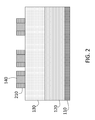
- FIG. 2 shows the intermediate structure that results from forming spacers formed on each side of each fin hard mask
- FIG. 3 is the result of performing an oxide fill in the gaps shown above the base in the structure shown in FIG. 2 ;
- FIG. 4 is a cross-sectional view of an intermediate structure that results from stripping of the spacers from the structure shown in FIG. 3 ;
- FIG. 5 is a cross-sectional view of an intermediate structure that results from a fin etch process
- FIG. 6 is a cross-sectional view of an intermediate structure that results from filling the trenches shown in FIG. 6 with a hard mask material;
- FIG. 7 results from an oxide strip to remove the oxide above the base in the structure shown in FIG. 6 ;
- FIG. 8 shows the result of etching the base and part of the doped layer below the base while retaining the fins and the hard mask buffer adjacent to the fins;
- FIG. 9 is a cross-sectional view of the intermediate structure resulting from removal of the hard mask adjacent to each fin;
- FIG. 10 shows the intermediate structure that results from the formation of a bottom spacer on the remaining doped layer
- FIG. 11 is a cross-sectional view of the intermediate structure that results from the formation of a metal layer on the bottom spacer;
- FIG. 12 is a cross-sectional view of the intermediate structure that results from the formation of a top spacer on the metal layer.
- FIG. 13 shows the cross-sectional view of an intermediate structure of a VFET with a layer deposited for formation of drain regions above the fins.
- Fin formation is one of the processes performed during the fabrication of the FETs.
- Fin pitch refers to the distance from an edge of a fin to the same edge of an adjacent fin.
- the phrase “pitch walking” refers to the fact that the pitch between different sets of adjacent fins is unlikely to be precisely the same. Pitch walking results from the sideways image transfer process (e.g., from self-aligned double patterning (SADP)) used in fin formation. A consequence of pitch walking can be non-uniform fin heights. Pitch walking is an issue in all fin-based FETs.
- SADP self-aligned double patterning
- different fin pitches can be required by a design need (e.g., in different devices).
- the non-uniform channel height that can result from pitch walking and variable fin pitch design can cause device failure. This is because the same conditions that result in non-uniform fin heights because of pitch walking will also result in the gate lengths directly adjacent to each fin being different. This results in poor control by the gates in the channel region.
- one or more embodiments relate to forming spacers on either side of each fin hard mask pattern to define a uniform distance adjacent to each fin hard mask pattern. This spacer-defined uniform distance or uniform width is then used to form trenches around the fins that are the same depth. These trenches, in turn, facilitate obtaining fins of the same height. As a consequence, the gate length directly adjacent to each side of each fin (i.e., channel region) is the same.
- FIGS. 1-13 show cross-sectional views of intermediate structures involved in the formation of a FET with uniform fin height.
- FIG. 10-13 are associated with one or more embodiments that are specific to the formation of a VFET.
- FIG. 1 is a cross-sectional view of an intermediate structure with fin hard masks 140 formed on a base 130 (e.g., silicon (Si)).
- the fin hard masks 140 result from a known patterning of a fin hard mask 140 layer.
- the fin hard mask 140 is a material that is resistant to the etch process used to etch the base 130 to form the fins 510 ( FIG. 5 ).
- the fin hard mask 140 can be silicon nitride (SiN), silicon dioxide (SiO 2 ), or a high k metal oxide dielectric (e.g., titanium oxide (TiO 2 ), hafnium oxide (HfO 2 ), or aluminum oxide (Al 2 O 3 )), for example.
- a metal oxide dielectric e.g., titanium oxide (TiO 2 ), hafnium oxide (HfO 2 ), or aluminum oxide (Al 2 O 3 )
- the base 130 is formed on a doped layer 120 (e.g., nitrogen (N+)) that is formed on a substrate 110 .
- the doped layer 120 forms the source region or, in alternate embodiments, the drain region of the device.
- the substrate 110 is a silicon substrate, for example.
- the semiconductor substrate 110 can also include an organic semiconductor or a layered semiconductor such as, for example, Si/SiGe, a silicon-on-insulator or a SiGe-on-insulator.
- a portion or entire semiconductor substrate 110 can be amorphous, polycrystalline, or monocrystalline.
- the semiconductor substrate 110 can also include a hybrid oriented (HOT) semiconductor substrate in which the HOT substrate has surface regions of different crystallographic orientation.
- the semiconductor substrate 110 can be doped, undoped, or contain doped regions and undoped regions therein.
- the semiconductor substrate 110 can contain regions with strain and regions without strain therein, or contain regions of tensile strain and compressive strain.
- the substrate 110 can be a semiconductor-on-insulator (SOI) substrate.
- SOI semiconductor-on-insulator
- the substrate 110 can further include other structures (not shown) such as shallow trench isolation (STI), fins, nanowires, nanosheets, resistors, capacitors, etc.
- STI shallow trench isolation
- FIG. 2 results from the formation of spacers 210 on each side of each fin hard mask 140 shown in FIG. 1 .
- the spacers 210 can be amorphous carbon (aC).
- the spacers 210 result from a conformal coating of the spacer material followed by etching such as by a reactive ion etch (ME) process.
- the intermediate structure shown in FIG. 3 results from an oxide 310 fill in the gaps left adjacent to the spacers 210 in the intermediate structure shown in FIG. 2 .
- a planarization such as a chemical mechanical planarization (CMP), can be performed on the oxide 310 .
- CMP chemical mechanical planarization
- FIG. 4 is a cross-sectional view of an intermediate structure that results from stripping of the spacers 210 from the structure shown in FIG. 3 .
- a isotropic etch e.g., RIE
- FIG. 4 indicates, based on the width of each of the removed spacers 210 being the same, the width of the gap 410 around each fin hard mask 140 , which results from the removal of the spacers 210 , is the same.
- FIG. 5 is a cross-sectional view of an intermediate structure that results from a fin 510 etch process.
- the portions of the base 130 with the surface uncovered by either the fin hard mask 140 or the oxide 310 are etched through, as is part of the doped layer 120 .
- the uniformity of the spacers 210 i.e., their thickness being the same
- the depth of the etch performed using the ME process is a function of the width of the space being etched.
- the space on either side of each fin hard mask 140 is exactly the same width because of the uniform spacers 210 .
- the depth of each trench 520 and, consequently, the height of each fin 510 is the same.
- the trenches 520 in the structure shown in FIG. 5 are filled with a hard mask 610 to result in the intermediate structure shown in FIG. 6 .
- the hard mask 610 can be the same material as the fin hard mask 140 according to one or more embodiments.
- An oxide 310 strip results in the intermediate structure shown in FIG. 7 .
- the etch results in non-uniform recessing of the doped layer 120 .
- This non-uniform etching illustrates the issue that is addressed by the uniform spacers 210 .
- the trench 810 is deeper than the trench 820 because the trench 810 is wider than the trench 820 .
- the RIE process is performed to form the fins 510 , the space left by the uniform spacers 210 (see e.g., FIG. 4 ) is the same width adjacent to each fin hard mask 140 .
- each trench 510 is the same.
- the RIE process that results in the structure shown in FIG. 8 does not affect the fins 510 , because the fins 510 are buffered by the hard masks 140 above and the hard masks 610 on each side.
- FIG. 9 is a cross-sectional view of the intermediate structure resulting from removal of the hard mask 610 adjacent to each fin 510 .
- known processes for fabricating a finFET can be continued. While these known processes are not detailed, some of the processes that are specific to the fabrication of a VFET are outlined with reference to FIGS. 10-13 .
- FIG. 10 shows the intermediate structure that results from the formation of a bottom spacer 1010 on the remaining doped layer 120 .
- the bottom spacer 1010 can be silicon boron carbide nitride (SiBCN, SiN or Silicon oxide), for example.
- a high-k dielectric 1110 is formed on the bottom spacer 1010 , and a metal layer 1120 is formed on the high-k dielectric 1110 , as shown in FIG. 11 .
- metal Gate and high-k are recessed to below Fin top This metal layer 1120 functions as the gate.
- a top spacer 1210 is formed above the recessed gate metal layer 1110 , as shown in FIG. 12 .
- This top spacer 1210 can be the same material (e.g., SiBCN, SiN, Silicon oxide) as the bottom spacer 1010 .
- An interlayer dielectric (ILD) 1310 is then formed (e.g., deposited and a CMP process performed), as shown in FIG. 13 , the spacer material and fin hard mask 140 is removed from above the fins 510 , and an epitaxial layer 1320 is grown on each of the fins 510 .
- the drain regions or, in alternate embodiments in which the doped layer 120 is the drain region, the source regions associated with each fin 510 are formed in the epitaxial layers 1320 .
- the gate length which is the indicated gate height h (i.e., the height of the metal layer 1120 between the high-k dielectric 1110 and the top spacer 1210 ) that is directly adjacent to each side of each of the fins 510 , is substantially the same. This is because of the spacers 210 of uniform width that were placed adjacent to the fin hard mask 140 that defined the fin 510 regions.
- references in the present description to forming layer “A” over layer “B” include situations in which one or more intermediate layers (e.g., layer “C”) is between layer “A” and layer “B” as long as the relevant characteristics and functionalities of layer “A” and layer “B” are not substantially changed by the intermediate layer(s).
- layer “C” one or more intermediate layers
- compositions comprising, “comprising,” “includes,” “including,” “has,” “having,” “contains” or “containing,” or any other variation thereof, are intended to cover a non-exclusive inclusion.
- a composition, a mixture, process, method, article, or apparatus that comprises a list of elements is not necessarily limited to only those elements but can include other elements not expressly listed or inherent to such composition, mixture, process, method, article, or apparatus.
- connection can include an indirect “connection” and a direct “connection.”
- references in the specification to “one embodiment,” “an embodiment,” “an example embodiment,” etc., indicate that the embodiment described can include a particular feature, structure, or characteristic, but every embodiment may or may not include the particular feature, structure, or characteristic. Moreover, such phrases are not necessarily referring to the same embodiment. Further, when a particular feature, structure, or characteristic is described in connection with an embodiment, it is submitted that it is within the knowledge of one skilled in the art to affect such feature, structure, or characteristic in connection with other embodiments whether or not explicitly described.
- the terms “upper,” “lower,” “right,” “left,” “vertical,” “horizontal,” “top,” “bottom,” and derivatives thereof shall relate to the described structures and methods, as oriented in the drawing figures.
- the terms “overlying,” “atop,” “on top,” “positioned on” or “positioned atop” mean that a first element, such as a first structure, is present on a second element, such as a second structure, wherein intervening elements such as an interface structure can be present between the first element and the second element.
- the term “direct contact” means that a first element, such as a first structure, and a second element, such as a second structure, are connected without any intermediary conducting, insulating or semiconductor layers at the interface of the two elements.
- the term “selective to,” such as, for example, “a first element selective to a second element,” means that the first element can be etched and the second element can act as an etch stop.
- the terms “about,” “substantially,” “approximately,” and variations thereof are intended to include the degree of error associated with measurement of the particular quantity based upon the equipment available at the time of filing the application. For example, “about” can include a range of ⁇ 8% or 5%, or 2% of a given value.
- Deposition is any process that grows, coats, or otherwise transfers a material onto the wafer.
- Available technologies include physical vapor deposition (PVD), chemical vapor deposition (CVD), electrochemical deposition (ECD), molecular beam epitaxy (MBE) and more recently, atomic layer deposition (ALD) among others.
- Removal/etching is any process that removes material from the wafer. Examples include etch processes (either wet or dry), and chemical-mechanical planarization (CMP), and the like.
- Semiconductor doping is the modification of electrical properties by doping, for example, transistor sources and drains, generally by diffusion and/or by ion implantation. These doping processes are followed by furnace annealing or by rapid thermal annealing (RTA). Annealing serves to activate the implanted dopants. Films of both conductors (e.g., poly-silicon, aluminum, copper, etc.) and insulators (e.g., various forms of silicon dioxide, silicon nitride, etc.) are used to connect and isolate transistors and their components. Selective doping of various regions of the semiconductor substrate allows the conductivity of the substrate to be changed with the application of voltage.
- RTA rapid thermal annealing
- Semiconductor lithography is the formation of three-dimensional relief images or patterns on the semiconductor substrate for subsequent transfer of the pattern to the substrate.
- the patterns are formed by a light sensitive polymer called a photo-resist.
- lithography and etch pattern transfer steps are repeated multiple times. Each pattern being printed on the wafer is aligned to the previously formed patterns and slowly the conductors, insulators and selectively doped regions are built up to form the final device.
Landscapes
- Engineering & Computer Science (AREA)
- Power Engineering (AREA)
- Microelectronics & Electronic Packaging (AREA)
- Physics & Mathematics (AREA)
- Condensed Matter Physics & Semiconductors (AREA)
- General Physics & Mathematics (AREA)
- Computer Hardware Design (AREA)
- Ceramic Engineering (AREA)
- Manufacturing & Machinery (AREA)
- Plasma & Fusion (AREA)
- Insulated Gate Type Field-Effect Transistor (AREA)
Abstract
A method of fabricating a vertical field effect transistor includes forming a base layer on a doped layer that is formed on a substrate, and forming fin hard masks above the base layer. Spacers are formed adjacent to each side of each of the fin hard masks above the base layer. A width dimension of each of the spacers is the same. Gaps between the spacers are filled with oxide prior to removing the spacers. The spacers are removed to leave gaps of the same width on each side of each of the fin hard masks. An etch in the gaps forms a plurality of fins below the fin hard masks. A height dimension of each of the plurality of fins is the same and a space between two of the plurality of fins is different than a second space between two others of the plurality of fins.
Description
The present invention relates to the fabrication of a field effect transistor (FET), and more specifically, to obtaining uniform get length in vertical FETs (VFETs).
A FET is a three-terminal device that includes a source, drain, and gate. Generally, a FET is fabricated with the source and drain formed on the same lateral level such that current flow, which is controlled by the gate in the channel region between the source and drain regions, is horizontal. In the efforts to scale complementary metal-oxide semiconductor (CMOS) technologies to 5 nanometers and beyond, non-planar FET architectures such as fin-type FETs (finFETs) and vertical FETs (VFETs) have been pursued. In a finFET, the source, drain and channel regions are built as a three-dimensional fin, which serves as the body of the device. The gate electrode is wrapped over the top and sides of the fin, and the portion of the fin that is under the gate electrode functions as the channel. In a VFET, the channel is also formed in a three-dimensional fin. However, the gate in a VFET extends along and/or around the vertical sidewalls of the fin. As a result, current flow in the channel region is vertical rather than horizontal.
According to one or more embodiments of the present invention, a method of fabricating a vertical field effect transistor (VFET) includes forming a doped layer on a substrate, forming a base layer on the doped layer, and forming fin hard masks above the base layer. A space between two of the fin hard masks is different than a second space between two others of the fin hard masks. Uniform spacers are formed adjacent to each side of each of the fin hard masks above the base layer. A width dimension of each of the uniform spacers is substantially the same. First gaps between the uniform spacers are filled with oxide prior to removing the uniform spacers. Removing the uniform spacers leaves second gaps of substantially the same width on each side of each of the fin hard masks. An etch in the second gaps forms a plurality of fins below the fin hard masks. A height dimension of each of the plurality of fins is substantially the same and a space between two of the plurality of fins is different than a second space between two others of the plurality of fins.
According to one or more embodiments, a structure of a vertical field effect transistor (VFET) includes a substrate, and a doped layer formed on the substrate. A top surface of the doped layer is non-uniform. A plurality of fins is formed above the doped layer. A space between two of the plurality of fins is different than another space between another two of the plurality of fins. Gate metal is formed adjacent to each side of each of the plurality of fins. A height of the gate metal directly adjacent to each side of each of the plurality of fins is substantially the same.
The subject matter which is regarded as the invention is particularly pointed out and distinctly claimed in the claims at the conclusion of the specification. The forgoing and other features, and advantages of the invention are apparent from the following detailed description taken in conjunction with the accompanying drawings in which:
As previously noted, several non-planar FET architectures, such as finFETs and VFETs, have fin-shaped channel regions between the source and drain regions. Fin formation is one of the processes performed during the fabrication of the FETs. Fin pitch refers to the distance from an edge of a fin to the same edge of an adjacent fin. The phrase “pitch walking” refers to the fact that the pitch between different sets of adjacent fins is unlikely to be precisely the same. Pitch walking results from the sideways image transfer process (e.g., from self-aligned double patterning (SADP)) used in fin formation. A consequence of pitch walking can be non-uniform fin heights. Pitch walking is an issue in all fin-based FETs. In some cases, different fin pitches can be required by a design need (e.g., in different devices). In VFETs, the non-uniform channel height that can result from pitch walking and variable fin pitch design can cause device failure. This is because the same conditions that result in non-uniform fin heights because of pitch walking will also result in the gate lengths directly adjacent to each fin being different. This results in poor control by the gates in the channel region.
Turning now to an overview of aspects of the present invention, one or more embodiments relate to forming spacers on either side of each fin hard mask pattern to define a uniform distance adjacent to each fin hard mask pattern. This spacer-defined uniform distance or uniform width is then used to form trenches around the fins that are the same depth. These trenches, in turn, facilitate obtaining fins of the same height. As a consequence, the gate length directly adjacent to each side of each fin (i.e., channel region) is the same.
Turning now to a more detailed description of one or more embodiments, FIGS. 1-13 show cross-sectional views of intermediate structures involved in the formation of a FET with uniform fin height. FIG. 10-13 are associated with one or more embodiments that are specific to the formation of a VFET. FIG. 1 is a cross-sectional view of an intermediate structure with fin hard masks 140 formed on a base 130 (e.g., silicon (Si)). The fin hard masks 140 result from a known patterning of a fin hard mask 140 layer. The fin hard mask 140 is a material that is resistant to the etch process used to etch the base 130 to form the fins 510 (FIG. 5 ). The fin hard mask 140 can be silicon nitride (SiN), silicon dioxide (SiO2), or a high k metal oxide dielectric (e.g., titanium oxide (TiO2), hafnium oxide (HfO2), or aluminum oxide (Al2O3)), for example. As FIG. 1 indicates, the distance d1 between two adjacent fin hard masks 140 is different than the distance d2 between two other adjacent fin hard masks 140. This difference illustrates the pitch walking that was previously discussed. The base 130 is formed on a doped layer 120 (e.g., nitrogen (N+)) that is formed on a substrate 110. The doped layer 120 forms the source region or, in alternate embodiments, the drain region of the device.
The substrate 110 is a silicon substrate, for example. The base 130 is a fin channel material which can include bulk semiconductor, such as silicon, germanium, silicon germanium, silicon carbide, and those consisting essentially of III-V compound semiconductors having a composition defined by the formula AlX1GaX2InX3AsY1PY2NY3SbY4, where X1, X2, X3, Y1, Y2, Y3, and Y4 represent relative proportions, each greater than or equal to zero and X1+X2+X3+Y1+Y2+Y3+Y4=1 (1 being the total relative mole quantity). Other suitable substrates 110 include II-VI compound semiconductors having a composition ZnA1CdA2SeB1TeB2, where A1, A2, B1, and B2 are relative proportions each greater than or equal to zero and A1+A2+B1+B2=1 (1 being a total mole quantity). The semiconductor substrate 110 can also include an organic semiconductor or a layered semiconductor such as, for example, Si/SiGe, a silicon-on-insulator or a SiGe-on-insulator. A portion or entire semiconductor substrate 110 can be amorphous, polycrystalline, or monocrystalline. In addition to the aforementioned types of semiconductor substrates 110, the semiconductor substrate 110 can also include a hybrid oriented (HOT) semiconductor substrate in which the HOT substrate has surface regions of different crystallographic orientation. The semiconductor substrate 110 can be doped, undoped, or contain doped regions and undoped regions therein. The semiconductor substrate 110 can contain regions with strain and regions without strain therein, or contain regions of tensile strain and compressive strain. In one or more embodiments, the substrate 110 can be a semiconductor-on-insulator (SOI) substrate. The substrate 110 can further include other structures (not shown) such as shallow trench isolation (STI), fins, nanowires, nanosheets, resistors, capacitors, etc.
The trenches 520 in the structure shown in FIG. 5 are filled with a hard mask 610 to result in the intermediate structure shown in FIG. 6 . The hard mask 610 can be the same material as the fin hard mask 140 according to one or more embodiments.
An oxide 310 strip results in the intermediate structure shown in FIG. 7 . This is followed by an etch (e.g., RIE process) of the base 130 and part of the doped layer 120 to result in the intermediate structure shown in FIG. 8 . As FIG. 8 indicates, the etch results in non-uniform recessing of the doped layer 120. This non-uniform etching illustrates the issue that is addressed by the uniform spacers 210. The trench 810 is deeper than the trench 820 because the trench 810 is wider than the trench 820. When the RIE process is performed to form the fins 510, the space left by the uniform spacers 210 (see e.g., FIG. 4 ) is the same width adjacent to each fin hard mask 140. Thus, the depth of each trench 510 is the same. The RIE process that results in the structure shown in FIG. 8 does not affect the fins 510, because the fins 510 are buffered by the hard masks 140 above and the hard masks 610 on each side.
In FIG. 13 , the gate length, which is the indicated gate height h (i.e., the height of the metal layer 1120 between the high-k dielectric 1110 and the top spacer 1210) that is directly adjacent to each side of each of the fins 510, is substantially the same. This is because of the spacers 210 of uniform width that were placed adjacent to the fin hard mask 140 that defined the fin 510 regions.
Various embodiments of the present invention are described herein with reference to the related drawings. Alternative embodiments can be devised without departing from the scope of this invention. It is noted that various connections and positional relationships (e.g., over, below, adjacent, etc.) are set forth between elements in the following description and in the drawings. These connections and/or positional relationships, unless specified otherwise, can be direct or indirect, and the present invention is not intended to be limiting in this respect. Accordingly, a coupling of entities can refer to either a direct or an indirect coupling, and a positional relationship between entities can be a direct or indirect positional relationship. As an example of an indirect positional relationship, references in the present description to forming layer “A” over layer “B” include situations in which one or more intermediate layers (e.g., layer “C”) is between layer “A” and layer “B” as long as the relevant characteristics and functionalities of layer “A” and layer “B” are not substantially changed by the intermediate layer(s).
The following definitions and abbreviations are to be used for the interpretation of the claims and the specification. As used herein, the terms “comprises,” “comprising,” “includes,” “including,” “has,” “having,” “contains” or “containing,” or any other variation thereof, are intended to cover a non-exclusive inclusion. For example, a composition, a mixture, process, method, article, or apparatus that comprises a list of elements is not necessarily limited to only those elements but can include other elements not expressly listed or inherent to such composition, mixture, process, method, article, or apparatus.
Additionally, the term “exemplary” is used herein to mean “serving as an example, instance or illustration.” Any embodiment or design described herein as “exemplary” is not necessarily to be construed as preferred or advantageous over other embodiments or designs. The terms “at least one” and “one or more” are understood to include any integer number greater than or equal to one, i.e. one, two, three, four, etc. The terms “a plurality” are understood to include any integer number greater than or equal to two, i.e. two, three, four, five, etc. The term “connection” can include an indirect “connection” and a direct “connection.”
References in the specification to “one embodiment,” “an embodiment,” “an example embodiment,” etc., indicate that the embodiment described can include a particular feature, structure, or characteristic, but every embodiment may or may not include the particular feature, structure, or characteristic. Moreover, such phrases are not necessarily referring to the same embodiment. Further, when a particular feature, structure, or characteristic is described in connection with an embodiment, it is submitted that it is within the knowledge of one skilled in the art to affect such feature, structure, or characteristic in connection with other embodiments whether or not explicitly described.
For purposes of the description hereinafter, the terms “upper,” “lower,” “right,” “left,” “vertical,” “horizontal,” “top,” “bottom,” and derivatives thereof shall relate to the described structures and methods, as oriented in the drawing figures. The terms “overlying,” “atop,” “on top,” “positioned on” or “positioned atop” mean that a first element, such as a first structure, is present on a second element, such as a second structure, wherein intervening elements such as an interface structure can be present between the first element and the second element. The term “direct contact” means that a first element, such as a first structure, and a second element, such as a second structure, are connected without any intermediary conducting, insulating or semiconductor layers at the interface of the two elements. It should be noted that the term “selective to,” such as, for example, “a first element selective to a second element,” means that the first element can be etched and the second element can act as an etch stop. The terms “about,” “substantially,” “approximately,” and variations thereof are intended to include the degree of error associated with measurement of the particular quantity based upon the equipment available at the time of filing the application. For example, “about” can include a range of ±8% or 5%, or 2% of a given value.
For the sake of brevity, conventional techniques related to semiconductor device and integrated circuit (IC) fabrication may or may not be described in detail herein. Moreover, the various tasks and process steps described herein can be incorporated into a more comprehensive procedure or process having additional steps or functionality not described in detail herein. In particular, various steps in the manufacture of semiconductor devices and semiconductor-based ICs are well known and so, in the interest of brevity, many conventional steps will only be mentioned briefly herein or will be omitted entirely without providing the well-known process details.
By way of background, however, a more general description of the semiconductor device fabrication processes that can be utilized in implementing one or more embodiments of the present invention will now be provided. Although specific fabrication operations used in implementing one or more embodiments of the present invention can be individually known, the described combination of operations and/or resulting structures of the present invention are unique. Thus, the unique combination of the operations described in connection with the fabrication of a semiconductor device according to the present invention utilize a variety of individually known physical and chemical processes performed on a semiconductor (e.g., silicon) substrate, some of which are described in the immediately following paragraphs.
In general, the various processes used to form a micro-chip that will be packaged into an IC fall into four general categories, namely, film deposition, removal/etching, semiconductor doping and patterning/lithography. Deposition is any process that grows, coats, or otherwise transfers a material onto the wafer. Available technologies include physical vapor deposition (PVD), chemical vapor deposition (CVD), electrochemical deposition (ECD), molecular beam epitaxy (MBE) and more recently, atomic layer deposition (ALD) among others. Removal/etching is any process that removes material from the wafer. Examples include etch processes (either wet or dry), and chemical-mechanical planarization (CMP), and the like. Semiconductor doping is the modification of electrical properties by doping, for example, transistor sources and drains, generally by diffusion and/or by ion implantation. These doping processes are followed by furnace annealing or by rapid thermal annealing (RTA). Annealing serves to activate the implanted dopants. Films of both conductors (e.g., poly-silicon, aluminum, copper, etc.) and insulators (e.g., various forms of silicon dioxide, silicon nitride, etc.) are used to connect and isolate transistors and their components. Selective doping of various regions of the semiconductor substrate allows the conductivity of the substrate to be changed with the application of voltage. By creating structures of these various components, millions of transistors can be built and wired together to form the complex circuitry of a modern microelectronic device. Semiconductor lithography is the formation of three-dimensional relief images or patterns on the semiconductor substrate for subsequent transfer of the pattern to the substrate. In semiconductor lithography, the patterns are formed by a light sensitive polymer called a photo-resist. To build the complex structures that make up a transistor and the many wires that connect the millions of transistors of a circuit, lithography and etch pattern transfer steps are repeated multiple times. Each pattern being printed on the wafer is aligned to the previously formed patterns and slowly the conductors, insulators and selectively doped regions are built up to form the final device.
Claims (13)
1. A method of fabricating a vertical field effect transistor (VFET), the method comprising:
forming a doped layer on a substrate;
forming a base layer on the doped layer;
forming fin hard masks above the base layer, wherein a space between two of the fin hard masks is different than a second space between two others of the fin hard masks;
forming uniform spacers adjacent to each side of each of the fin hard masks above the base layer, wherein a width dimension of each of the uniform spacers is substantially the same;
filling first gaps between the uniform spacers with oxide prior to removing the uniform spacers, wherein the removing the uniform spacers leaves second gaps of substantially the same width on each side of each of the fin hard masks; and
performing an etch in the second gaps to form a plurality of fins below the fin hard masks, wherein a height dimension of each of the plurality of fins is substantially the same and a space between two of the plurality of fins is different than a second space between two others of the plurality of fins.
2. The method according to claim 1 , wherein the forming the doped layer includes forming a source region or a drain region.
3. The method according to claim 1 , wherein the forming the spacers includes forming amorphous carbon (aC) spacers.
4. The method according to claim 1 , wherein the performing the etch includes performing a reactive ion etch (RIE) process.
5. The method according to claim 4 , wherein the performing the RIE process includes etching the base layer and a partial depth of the doped layer below the second gaps to form trenches adjacent to each side of each of the plurality of fins.
6. The method according to claim 5 , further comprising forming hard mask spacers in the trenches adjacent to each side of each of the plurality of fins, wherein the hard mask spacers include width dimensions that are substantially the same and height dimensions that are substantially the same.
7. The method according to claim 6 , wherein the forming the hard mask spacers includes forming the hard mask spacers from a same material as the fin hard masks.
8. The method according to claim 1 , further comprising removing the oxide following formation of the plurality of fins and etching the base layer and a portion of the doped layer below the oxide, wherein the etching the portion of the doped layer results in a non-uniform top surface of the portion of the doped layer and no change in the plurality of fins and the hard mask spacers.
9. The method according to claim 8 , further comprising removing the hard mask spacers following the etching the base layer and the portion of the doped layer.
10. The method according to claim 8 , further comprising forming a bottom spacer on the non-uniform top surface of the doped layer.
11. The method according to claim 10 , further comprising forming a gate above the bottom spacer.
12. The method according to claim 11 , further comprising forming a top spacer above the gate.
13. The method according to claim 12 , further comprising forming a drain region or a source region above the top spacer based on the doped layer being, respectively, the source region or the drain region.
Priority Applications (2)
| Application Number | Priority Date | Filing Date | Title |
|---|---|---|---|
| US15/292,423 US9728635B1 (en) | 2016-10-13 | 2016-10-13 | Uniform gate length in vertical field effect transistors |
| US15/586,370 US9893181B1 (en) | 2016-10-13 | 2017-05-04 | Uniform gate length in vertical field effect transistors |
Applications Claiming Priority (1)
| Application Number | Priority Date | Filing Date | Title |
|---|---|---|---|
| US15/292,423 US9728635B1 (en) | 2016-10-13 | 2016-10-13 | Uniform gate length in vertical field effect transistors |
Related Child Applications (1)
| Application Number | Title | Priority Date | Filing Date |
|---|---|---|---|
| US15/586,370 Division US9893181B1 (en) | 2016-10-13 | 2017-05-04 | Uniform gate length in vertical field effect transistors |
Publications (1)
| Publication Number | Publication Date |
|---|---|
| US9728635B1 true US9728635B1 (en) | 2017-08-08 |
Family
ID=59410756
Family Applications (2)
| Application Number | Title | Priority Date | Filing Date |
|---|---|---|---|
| US15/292,423 Active US9728635B1 (en) | 2016-10-13 | 2016-10-13 | Uniform gate length in vertical field effect transistors |
| US15/586,370 Active US9893181B1 (en) | 2016-10-13 | 2017-05-04 | Uniform gate length in vertical field effect transistors |
Family Applications After (1)
| Application Number | Title | Priority Date | Filing Date |
|---|---|---|---|
| US15/586,370 Active US9893181B1 (en) | 2016-10-13 | 2017-05-04 | Uniform gate length in vertical field effect transistors |
Country Status (1)
| Country | Link |
|---|---|
| US (2) | US9728635B1 (en) |
Cited By (10)
| Publication number | Priority date | Publication date | Assignee | Title |
|---|---|---|---|---|
| US20170012126A1 (en) * | 2014-03-28 | 2017-01-12 | Intel Corporation | Selectively regrown top contact for vertical semiconductor devices |
| US20170317211A1 (en) * | 2016-04-29 | 2017-11-02 | Samsung Electronics Co., Ltd. | Vertical field effect transistor and method of fabricating the same |
| US10217846B1 (en) | 2018-01-17 | 2019-02-26 | Globalfoundries Inc. | Vertical field effect transistor formation with critical dimension control |
| US10249731B1 (en) * | 2017-09-25 | 2019-04-02 | International Business Macines Corporation | Vertical FET with sharp junctions |
| US10263077B1 (en) * | 2017-12-22 | 2019-04-16 | Commissariat A L'energie Atomique Et Aux Energies Alternatives | Method of fabricating a FET transistor having a strained channel |
| US10332983B1 (en) * | 2018-03-26 | 2019-06-25 | International Business Machines Corporation | Vertical field-effect transistors including uniform gate lengths |
| US10629702B2 (en) * | 2017-02-06 | 2020-04-21 | International Business Machines Corporation | Approach to bottom dielectric isolation for vertical transport fin field effect transistors |
| US10734245B2 (en) * | 2018-10-19 | 2020-08-04 | International Business Machines Corporation | Highly selective dry etch process for vertical FET STI recess |
| US10886367B2 (en) | 2019-01-17 | 2021-01-05 | International Business Machines Corporation | Forming FinFET with reduced variability |
| US11201092B2 (en) | 2019-03-27 | 2021-12-14 | International Business Machines Corporation | Gate channel length control in VFET |
Citations (12)
| Publication number | Priority date | Publication date | Assignee | Title |
|---|---|---|---|---|
| US20050029556A1 (en) | 2003-08-08 | 2005-02-10 | Ping-Wei Wang | Compact SRAM cell with FinFET |
| US7009250B1 (en) | 2004-08-20 | 2006-03-07 | Micron Technology, Inc. | FinFET device with reduced DIBL |
| US20110227145A1 (en) | 2010-03-19 | 2011-09-22 | Shing-Hwa Renn | Dual vertical channel transistor and fabrication method thereof |
| US9034723B1 (en) * | 2013-11-25 | 2015-05-19 | Taiwan Semiconductor Manufacturing Company, Ltd. | Method of making a FinFET device |
| US20150325692A1 (en) | 2014-05-06 | 2015-11-12 | Globalfoundries Inc. | Fin field effect transistor (finfet) device including a set of merged fins formed adjacent a set of unmerged fins |
| US9287135B1 (en) | 2015-05-26 | 2016-03-15 | International Business Machines Corporation | Sidewall image transfer process for fin patterning |
| US9299835B1 (en) | 2014-12-04 | 2016-03-29 | International Business Machines Corporation | Vertical field effect transistors |
| US20160148931A1 (en) | 2014-11-24 | 2016-05-26 | International Business Machines Corporation | Dual epitaxy cmos processing using selective nitride formation for reduced gate pitch |
| US9368572B1 (en) | 2015-11-21 | 2016-06-14 | International Business Machines Corporation | Vertical transistor with air-gap spacer |
| US9397226B2 (en) | 2014-11-21 | 2016-07-19 | International Business Machines Corporation | Vertical field effect transistors with controlled overlap between gate electrode and source/drain contacts |
| US20160254191A1 (en) * | 2015-02-26 | 2016-09-01 | Taiwan Semiconductor Manufacturing Company, Ltd. | Fin patterning methods for increased process margin |
| US20160307769A1 (en) * | 2015-04-17 | 2016-10-20 | Taiwan Semiconductor Manufacturing Company, Ltd. | Lithographic Technique Incorporating Varied Pattern Materials |
Family Cites Families (1)
| Publication number | Priority date | Publication date | Assignee | Title |
|---|---|---|---|---|
| US10084080B2 (en) * | 2015-03-31 | 2018-09-25 | Stmicroelectronics, Inc. | Vertical tunneling FinFET |
-
2016
- 2016-10-13 US US15/292,423 patent/US9728635B1/en active Active
-
2017
- 2017-05-04 US US15/586,370 patent/US9893181B1/en active Active
Patent Citations (14)
| Publication number | Priority date | Publication date | Assignee | Title |
|---|---|---|---|---|
| US20050029556A1 (en) | 2003-08-08 | 2005-02-10 | Ping-Wei Wang | Compact SRAM cell with FinFET |
| US6924560B2 (en) | 2003-08-08 | 2005-08-02 | Taiwan Semiconductor Manufacturing Co., Ltd. | Compact SRAM cell with FinFET |
| US7009250B1 (en) | 2004-08-20 | 2006-03-07 | Micron Technology, Inc. | FinFET device with reduced DIBL |
| US20110227145A1 (en) | 2010-03-19 | 2011-09-22 | Shing-Hwa Renn | Dual vertical channel transistor and fabrication method thereof |
| US8653584B2 (en) | 2010-03-19 | 2014-02-18 | Nanya Technology Corp. | Dual vertical channel transistor and fabrication method thereof |
| US9034723B1 (en) * | 2013-11-25 | 2015-05-19 | Taiwan Semiconductor Manufacturing Company, Ltd. | Method of making a FinFET device |
| US20150325692A1 (en) | 2014-05-06 | 2015-11-12 | Globalfoundries Inc. | Fin field effect transistor (finfet) device including a set of merged fins formed adjacent a set of unmerged fins |
| US9397226B2 (en) | 2014-11-21 | 2016-07-19 | International Business Machines Corporation | Vertical field effect transistors with controlled overlap between gate electrode and source/drain contacts |
| US20160148931A1 (en) | 2014-11-24 | 2016-05-26 | International Business Machines Corporation | Dual epitaxy cmos processing using selective nitride formation for reduced gate pitch |
| US9299835B1 (en) | 2014-12-04 | 2016-03-29 | International Business Machines Corporation | Vertical field effect transistors |
| US20160254191A1 (en) * | 2015-02-26 | 2016-09-01 | Taiwan Semiconductor Manufacturing Company, Ltd. | Fin patterning methods for increased process margin |
| US20160307769A1 (en) * | 2015-04-17 | 2016-10-20 | Taiwan Semiconductor Manufacturing Company, Ltd. | Lithographic Technique Incorporating Varied Pattern Materials |
| US9287135B1 (en) | 2015-05-26 | 2016-03-15 | International Business Machines Corporation | Sidewall image transfer process for fin patterning |
| US9368572B1 (en) | 2015-11-21 | 2016-06-14 | International Business Machines Corporation | Vertical transistor with air-gap spacer |
Non-Patent Citations (1)
| Title |
|---|
| Yakimets et al., "Vertical GAAFETs for the Ultimate CMOS Scaling", IEEE Transactions on Electron Devices, vol. 62, No. 5, May 2015, pp. 1433-1439. |
Cited By (13)
| Publication number | Priority date | Publication date | Assignee | Title |
|---|---|---|---|---|
| US20170012126A1 (en) * | 2014-03-28 | 2017-01-12 | Intel Corporation | Selectively regrown top contact for vertical semiconductor devices |
| US10727339B2 (en) * | 2014-03-28 | 2020-07-28 | Intel Corporation | Selectively regrown top contact for vertical semiconductor devices |
| US20170317211A1 (en) * | 2016-04-29 | 2017-11-02 | Samsung Electronics Co., Ltd. | Vertical field effect transistor and method of fabricating the same |
| US10032906B2 (en) * | 2016-04-29 | 2018-07-24 | Samsung Electronics Co., Ltd. | Vertical field effect transistor and method of fabricating the same |
| US10840354B2 (en) | 2017-02-06 | 2020-11-17 | International Business Machines Corporation | Approach to bottom dielectric isolation for vertical transport fin field effect transistors |
| US10629702B2 (en) * | 2017-02-06 | 2020-04-21 | International Business Machines Corporation | Approach to bottom dielectric isolation for vertical transport fin field effect transistors |
| US10249731B1 (en) * | 2017-09-25 | 2019-04-02 | International Business Macines Corporation | Vertical FET with sharp junctions |
| US10263077B1 (en) * | 2017-12-22 | 2019-04-16 | Commissariat A L'energie Atomique Et Aux Energies Alternatives | Method of fabricating a FET transistor having a strained channel |
| US10217846B1 (en) | 2018-01-17 | 2019-02-26 | Globalfoundries Inc. | Vertical field effect transistor formation with critical dimension control |
| US10332983B1 (en) * | 2018-03-26 | 2019-06-25 | International Business Machines Corporation | Vertical field-effect transistors including uniform gate lengths |
| US10734245B2 (en) * | 2018-10-19 | 2020-08-04 | International Business Machines Corporation | Highly selective dry etch process for vertical FET STI recess |
| US10886367B2 (en) | 2019-01-17 | 2021-01-05 | International Business Machines Corporation | Forming FinFET with reduced variability |
| US11201092B2 (en) | 2019-03-27 | 2021-12-14 | International Business Machines Corporation | Gate channel length control in VFET |
Also Published As
| Publication number | Publication date |
|---|---|
| US9893181B1 (en) | 2018-02-13 |
Similar Documents
| Publication | Publication Date | Title |
|---|---|---|
| US9893181B1 (en) | Uniform gate length in vertical field effect transistors | |
| US9741626B1 (en) | Vertical transistor with uniform bottom spacer formed by selective oxidation | |
| US9735160B2 (en) | Method of co-integration of strained silicon and strained germanium in semiconductor devices including fin structures | |
| US10002939B1 (en) | Nanosheet transistors having thin and thick gate dielectric material | |
| US9741716B1 (en) | Forming vertical and horizontal field effect transistors on the same substrate | |
| US10896851B2 (en) | Vertically stacked transistors | |
| US9728621B1 (en) | iFinFET | |
| US10325995B2 (en) | Field effect transistor air-gap spacers with an etch-stop layer | |
| US10388571B2 (en) | Fin type field effect transistors with different pitches and substantially uniform fin reveal | |
| US20180005895A1 (en) | Vertical transistor with variable gate length | |
| US10347657B1 (en) | Semiconductor circuit including nanosheets and fins on the same wafer | |
| US9620507B2 (en) | Silicon-on-nothing transistor semiconductor structure with channel epitaxial silicon-germanium region | |
| US9837403B1 (en) | Asymmetrical vertical transistor | |
| US20220375788A1 (en) | Formation of trench silicide source or drain contacts without gate damage | |
| US10297507B2 (en) | Self-aligned vertical field-effect transistor with epitaxially grown bottom and top source drain regions | |
| US10367061B1 (en) | Replacement metal gate and inner spacer formation in three dimensional structures using sacrificial silicon germanium | |
| US11348999B2 (en) | Nanosheet semiconductor devices with sigma shaped inner spacer | |
| US9793378B2 (en) | Fin field effect transistor device with reduced overlap capacitance and enhanced mechanical stability | |
| US10622264B2 (en) | Nanosheet devices with different types of work function metals | |
| US9748381B1 (en) | Pillar formation for heat dissipation and isolation in vertical field effect transistors | |
| US10665698B2 (en) | Reducing gate-induced-drain-leakage current in a transistor by forming an enhanced band gap layer at the channel-to-drain interface | |
| WO2023045480A1 (en) | Using different work-functions to reduce gate-induced drain leakage current in stacked nanosheet transistors | |
| US10319643B1 (en) | Vertical FET with strained channel | |
| US20230142410A1 (en) | Gate-all-around nanosheet-fet with variable channel geometries for performance optimization |
Legal Events
| Date | Code | Title | Description |
|---|---|---|---|
| AS | Assignment |
Owner name: INTERNATIONAL BUSINESS MACHINES CORPORATION, NEW Y Free format text: ASSIGNMENT OF ASSIGNORS INTEREST;ASSIGNORS:CHENG, KANGGUO;XU, PENG;REEL/FRAME:040005/0422 Effective date: 20161012 |
|
| STCF | Information on status: patent grant |
Free format text: PATENTED CASE |
|
| MAFP | Maintenance fee payment |
Free format text: PAYMENT OF MAINTENANCE FEE, 4TH YEAR, LARGE ENTITY (ORIGINAL EVENT CODE: M1551); ENTITY STATUS OF PATENT OWNER: LARGE ENTITY Year of fee payment: 4 |