US9696492B1 - On-chip photonic-phononic emitter-receiver apparatus - Google Patents
On-chip photonic-phononic emitter-receiver apparatus Download PDFInfo
- Publication number
- US9696492B1 US9696492B1 US15/060,388 US201615060388A US9696492B1 US 9696492 B1 US9696492 B1 US 9696492B1 US 201615060388 A US201615060388 A US 201615060388A US 9696492 B1 US9696492 B1 US 9696492B1
- Authority
- US
- United States
- Prior art keywords
- optical
- waveguide
- wave
- optical waveguide
- frequency
- Prior art date
- Legal status (The legal status is an assumption and is not a legal conclusion. Google has not performed a legal analysis and makes no representation as to the accuracy of the status listed.)
- Active
Links
Images


Classifications
-
- G—PHYSICS
- G02—OPTICS
- G02B—OPTICAL ELEMENTS, SYSTEMS OR APPARATUS
- G02B6/00—Light guides; Structural details of arrangements comprising light guides and other optical elements, e.g. couplings
- G02B6/10—Light guides; Structural details of arrangements comprising light guides and other optical elements, e.g. couplings of the optical waveguide type
- G02B6/12—Light guides; Structural details of arrangements comprising light guides and other optical elements, e.g. couplings of the optical waveguide type of the integrated circuit kind
- G02B6/122—Basic optical elements, e.g. light-guiding paths
- G02B6/1225—Basic optical elements, e.g. light-guiding paths comprising photonic band-gap structures or photonic lattices
-
- G—PHYSICS
- G02—OPTICS
- G02B—OPTICAL ELEMENTS, SYSTEMS OR APPARATUS
- G02B1/00—Optical elements characterised by the material of which they are made; Optical coatings for optical elements
- G02B1/002—Optical elements characterised by the material of which they are made; Optical coatings for optical elements made of materials engineered to provide properties not available in nature, e.g. metamaterials
- G02B1/005—Optical elements characterised by the material of which they are made; Optical coatings for optical elements made of materials engineered to provide properties not available in nature, e.g. metamaterials made of photonic crystals or photonic band gap materials
-
- G—PHYSICS
- G02—OPTICS
- G02F—OPTICAL DEVICES OR ARRANGEMENTS FOR THE CONTROL OF LIGHT BY MODIFICATION OF THE OPTICAL PROPERTIES OF THE MEDIA OF THE ELEMENTS INVOLVED THEREIN; NON-LINEAR OPTICS; FREQUENCY-CHANGING OF LIGHT; OPTICAL LOGIC ELEMENTS; OPTICAL ANALOGUE/DIGITAL CONVERTERS
- G02F1/00—Devices or arrangements for the control of the intensity, colour, phase, polarisation or direction of light arriving from an independent light source, e.g. switching, gating or modulating; Non-linear optics
- G02F1/01—Devices or arrangements for the control of the intensity, colour, phase, polarisation or direction of light arriving from an independent light source, e.g. switching, gating or modulating; Non-linear optics for the control of the intensity, phase, polarisation or colour
- G02F1/11—Devices or arrangements for the control of the intensity, colour, phase, polarisation or direction of light arriving from an independent light source, e.g. switching, gating or modulating; Non-linear optics for the control of the intensity, phase, polarisation or colour based on acousto-optical elements, e.g. using variable diffraction by sound or like mechanical waves
- G02F1/125—Devices or arrangements for the control of the intensity, colour, phase, polarisation or direction of light arriving from an independent light source, e.g. switching, gating or modulating; Non-linear optics for the control of the intensity, phase, polarisation or colour based on acousto-optical elements, e.g. using variable diffraction by sound or like mechanical waves in an optical waveguide structure
-
- G—PHYSICS
- G02—OPTICS
- G02F—OPTICAL DEVICES OR ARRANGEMENTS FOR THE CONTROL OF LIGHT BY MODIFICATION OF THE OPTICAL PROPERTIES OF THE MEDIA OF THE ELEMENTS INVOLVED THEREIN; NON-LINEAR OPTICS; FREQUENCY-CHANGING OF LIGHT; OPTICAL LOGIC ELEMENTS; OPTICAL ANALOGUE/DIGITAL CONVERTERS
- G02F2/00—Demodulating light; Transferring the modulation of modulated light; Frequency-changing of light
- G02F2/002—Demodulating light; Transferring the modulation of modulated light; Frequency-changing of light using optical mixing
-
- G—PHYSICS
- G02—OPTICS
- G02F—OPTICAL DEVICES OR ARRANGEMENTS FOR THE CONTROL OF LIGHT BY MODIFICATION OF THE OPTICAL PROPERTIES OF THE MEDIA OF THE ELEMENTS INVOLVED THEREIN; NON-LINEAR OPTICS; FREQUENCY-CHANGING OF LIGHT; OPTICAL LOGIC ELEMENTS; OPTICAL ANALOGUE/DIGITAL CONVERTERS
- G02F2/00—Demodulating light; Transferring the modulation of modulated light; Frequency-changing of light
- G02F2/004—Transferring the modulation of modulated light, i.e. transferring the information from one optical carrier of a first wavelength to a second optical carrier of a second wavelength, e.g. all-optical wavelength converter
-
- H—ELECTRICITY
- H04—ELECTRIC COMMUNICATION TECHNIQUE
- H04B—TRANSMISSION
- H04B1/00—Details of transmission systems, not covered by a single one of groups H04B3/00 - H04B13/00; Details of transmission systems not characterised by the medium used for transmission
- H04B1/38—Transceivers, i.e. devices in which transmitter and receiver form a structural unit and in which at least one part is used for functions of transmitting and receiving
- H04B1/40—Circuits
-
- G—PHYSICS
- G02—OPTICS
- G02B—OPTICAL ELEMENTS, SYSTEMS OR APPARATUS
- G02B6/00—Light guides; Structural details of arrangements comprising light guides and other optical elements, e.g. couplings
- G02B6/10—Light guides; Structural details of arrangements comprising light guides and other optical elements, e.g. couplings of the optical waveguide type
- G02B6/12—Light guides; Structural details of arrangements comprising light guides and other optical elements, e.g. couplings of the optical waveguide type of the integrated circuit kind
- G02B2006/12035—Materials
- G02B2006/12061—Silicon
-
- G—PHYSICS
- G02—OPTICS
- G02F—OPTICAL DEVICES OR ARRANGEMENTS FOR THE CONTROL OF LIGHT BY MODIFICATION OF THE OPTICAL PROPERTIES OF THE MEDIA OF THE ELEMENTS INVOLVED THEREIN; NON-LINEAR OPTICS; FREQUENCY-CHANGING OF LIGHT; OPTICAL LOGIC ELEMENTS; OPTICAL ANALOGUE/DIGITAL CONVERTERS
- G02F2202/00—Materials and properties
- G02F2202/32—Photonic crystals
Definitions
- the invention relates to radio-frequency photonic devices, and more particularly to devices that employ photon-phonon coupling for information transfer.
- U.S. Pat. No. 9,268,092 by R. L. Jarecki, Jr. et al. which issued on Feb. 23, 2016 under the title, “Guided Wave Opto-Acoustic Device,” and which is assigned at least in part to an assignee hereof, describes a suspended membrane device in which at least one optical waveguiding member is included in the membrane. At least one phononic resonator is defined in the membrane and traversed by the optical waveguiding member. Guided-wave, stimulated Brillouin scattering (SBS) in the device can be applied in various signal-processing applications.
- SBS stimulated Brillouin scattering
- resonant systems can achieve strong coupling and high frequency selectivity, they also suffer from disadvantages such as sensitivity to the optical wavelength.
- optical signals propagating in an emitter optical waveguide produce forces that transduce coherent phononic signals in the waveguide core.
- a phononic crystal (PnC) superstructure that surrounds the emitter optical waveguide and also surrounds a nearby receiver optical waveguide shapes the transfer of the phononic signal to the receiver optical waveguide.
- the receiver optical waveguide converts the signal from the acoustic domain back to the optical domain through photoelastic coupling.
- the transfer function that governs the phononic coupling between the emitter and receiver waveguides can be tailored by suitable engineering of the PnC superstructure. This enables the designer to control properties of the transduction process such as bandwidth, frequency, and conversion efficiency, even at RF frequencies in the gigahertz range.
- the phononic signal consists of acoustic waves of frequencies that lie within the band gap of the PnC and that are consequently confined, to some extent, to phononic crystal line defects in the vicinities of the optical waveguides.
- the transfer function therefore depends not only on the design of the PnC structure per se, but also on the modal structures of the line defects.
- the transduction of coherent phononic signals and the reconversion from the acoustic domain back to the optical domain take place within the same optical waveguide, rather than in separate emitter and receiver waveguides.
- the transfer function that governs the phononic coupling between the input and output optical signals (within the same waveguide) can be tailored by suitable engineering of the PnC superstructure responsible for phononic confinement, and especially by suitable engineering of the PnC line defect.
- the invention in an embodiment includes a membrane in which a two-dimensionally periodic phononic crystal (PnC) structure is patterned. At least a first optical waveguide is embedded in the membrane. At least a first line-defect region interrupts the PnC structure. The first optical waveguide is embedded within the line-defect region.
- PnC two-dimensionally periodic phononic crystal
- At least a first and a second optical waveguide are embedded in the membrane within line-defect regions that interrupt the PnC structure.
- the first and second optical waveguides are parallel to each other but have no substantial optical coupling to each other.
- a central region of the PnC structure lies between the first and second optical waveguides.
- an input end of the first optical waveguide is optically coupled to a path for an optical input carrier wave and an optical local oscillator wave
- an input end of the second optical waveguide is optically coupled to a path for an optical probe wave
- an output end of the second optical waveguide is optically coupled to a path for an output signal.
- the first optical waveguide is configured as a Fabry-Perot resonator cavity for the optical input carrier wave and the optical local oscillator wave.
- one or more further line-defect regions interrupt the PnC structure between the first optical waveguide and the second optical waveguide.
- Some embodiments are configured as frequency filters for radio-frequency (RF) signals modulated onto the optical input carrier wave from a signal source.
- RF radio-frequency
- Some embodiments are configured as wavelength converters for transferring radio-frequency (RF) signals from an optical input carrier wave of a first carrier wavelength propagating in the first optical waveguide to an optical carrier wave of a second carrier wavelength propagating in the second optical waveguide.
- RF radio-frequency
- Some embodiments are configured as amplifiers for transferring radio-frequency (RF) signals from an optical input carrier wave of a first intensity propagating in the first optical waveguide to an optical carrier wave of a second intensity propagating in the second optical waveguide.
- RF radio-frequency
- an optical input carrier wave and an optical local oscillator wave are coupled into the first waveguide, and a radio-frequency (RF) modulator is arranged to modulate an RF signal onto the optical input carrier wave.
- RF radio-frequency
- FIG. 1 is a schematic diagram of a PPER system consisting of two silicon optical waveguides embedded in a phononic crystal membrane.
- FIG. 2 is diagram illustrating the principle of PPER operation.
- the optical input signal, optical output signal and transduced phonon waves are represented in the figure.
- FIGS. 3-5 are representative spectra of the input ( 3 ) and output ( 5 ) optical signals and the response ( 4 ) produced by phononic supermodes that mediate information transfer.
- the transfer function of the phononic supermodes is indicated by shading in FIG. 5 .
- FIG. 6 is a schematic diagram illustrating the anatomy of a PnC-BAM waveguide, with indication of the wavevectors of the optical pump (k 1 ), the scattered light (k 2 ) and the phonon (K).
- FIG. 7 is a dispersion diagram of a 2D phononic crystal (PnC), showing the phonon frequency versus the phonon wave vector in the x-direction.
- An inset depicts the unit cell of the 2D PnC.
- FIG. 8 is a cross-sectional view, based on an SEM image, of the waveguide core within the nitride membrane of an example PPER device.
- FIG. 9 provides a spectrum of Brillouin responses of a representative PPER device obtained through heterodyne four-wave mixing measurements.
- the left-hand inset shows the schematic geometry of the PnC-BAM waveguide.
- FIG. 10 shows the computed E x fields of an optical mode in a silicon waveguide.
- FIG. 11 is a schematic drawing that shows the dual-channel PnC-BAM waveguide that forms a PPER system described here.
- FIG. 12 is a view, based on an SEM image, of a portion of the dual-channel PPER system of FIG. 11 .
- FIG. 13 is a schematic representation of the elastic displacement fields (for x-displacement) associated with symmetric and antisymmetric supermodes of a PPER system.
- FIG. 14 is a representative plot of the parametric responses for single-channel (dashed curve) and dual-channel (solid curve) PnC-BAM waveguides.
- FIG. 15 provides a pair of representative curves illustrating the displacement distributions for symmetric (I) and anti-symmetric (II) supermodes.
- FIG. 16 is a top-down view, based on a scanning electron microscopy (SEM) image, of a portion of a PnC-BAM waveguide.
- SEM scanning electron microscopy
- FIG. 17 is a schematic diagram of the apparatus used to measure the Brillouin nonlinearities of PnC-BAM waveguides in experiments that are reported here.
- FIG. 18 is a comparative plot of the normalized RF response of a PPER system.
- the solid curve represents experimental data, and the broken curve is a theoretical prediction.
- the system noise floor is represented by a dotted line near the bottom of the figure.
- FIG. 19 provides side-by-side plots of the measured RF responses of PPER systems having two different values of the defect width W o .
- W o 5.7 ⁇ m
- W o 5.2 ⁇ m.
- FIG. 20 in the main view, provides a plot of the coupling rate ⁇ versus the reciprocal of the net decay rate ⁇ net ⁇ 1 extracted from measured RF responses of four PPER systems having different design parameters. Results are shown in log-log scale.
- the inset in the top-left corner of the plot is the schematic geometry of the BAM waveguides.
- Insets I, II, III and IV in the right and bottom corners of the figure are the normalized RF power responses corresponding to the respective sets of design parameters.
- FIG. 21 is a plan view of an example design for an optical waveguide that has been conformed as a distributed Bragg reflector (DBR) cavity, which is useful for some of the embodiments described here.
- DBR distributed Bragg reflector
- FIG. 22 is a notional optical frequency spectrum illustrating an optical mixing technique according to certain principles described here.
- FIG. 23 is a schematic diagram providing an example of a multistage filter according to certain principles described here.
- FIG. 1 provides a perspective, schematic view of our new PPER system in an example embodiment.
- the drawing shows a substrate 10 and a silicon nitride membrane 15 suspended between supporting projections 20 , 25 .
- Two silicon optical waveguides are embedded in the membrane. They are emitter optical waveguide 30 and receiver optical waveguide 35 .
- the PnC structure is defined by a two-dimensional array of round holes 40 that perforate the membrane.
- the PnC structure includes symmetric PnC regions 45 and 50 that are placed outside the outer boundaries of the optical waveguides, and central PnC region 55 that is placed between the optical waveguides.
- Each of the optical waveguides is centered within a respective line defect region 60 , 65 .
- the line defect regions are elongated portions of the membrane that are “defects” in the PnC structure because they lack holes.
- the material system presented here which includes silicon waveguides and a silicon nitride membrane, is a non-limiting example.
- suitable waveguide materials including silicon nitride, germanium, chalcogenide glass, silicon dioxide, As 2 S 3 glass, and gallium arsenide and other III-V compounds.
- suitable membrane materials include silicon dioxide, silicon carbide, and alumina.
- the periodicity of the PnC structure gives rise to a band structure, including a band gap. Phonons having frequencies that fall within the band gap cannot propagate. Because each line defect is bounded on each side by a portion of the PnC structure, it is possible, in operation, for phonons having band-gap frequencies to be confined within the PnC line defects. Concurrently, the silicon waveguides within each PnC line defect are capable of guiding light by total internal reflection.
- the central PnC region 55 does not have perfect reflectivity. Because the reflectivity of that region is finite, there is evanescent coupling between the phononic defect modes of the emitter port and the phononic defect modes of the receiver port. This coupling can be controlled through suitable design of the PnC.
- the modes associated with the respective line defects hybridize to create joint patterns of excitation that we refer to as “supermodes”.
- the supermodes have frequency spectra that are distinct from the modal spectra of the individual, isolated line defects.
- the supermodes give rise to a multi-pole phononic transfer function for the coupled system.
- the multi-pole transfer functions that we have studied exhibit frequency selectivities that are far superior to singly resonant systems such as those described in Shin 2013. This is significant not least because of the advantages of such multi-pole transfer functions for high-performance signal processing applications.
- the exemplary dual-port PPER device topology of FIG. 1 is easily generalized; indeed, higher-order (e.g., third, fourth, and fifth order) responses can be produced by increasing the number of coupled line-defects.
- higher-order (e.g., third, fourth, and fifth order) responses can be produced by increasing the number of coupled line-defects.
- our new PPER device concept opens up a compelling new design space for hybrid photonic-phononic signal processing.
- FIG. 2 illustrates the operation of the example PPER device.
- Optical input signal 100 is shown propagating in emitter waveguide 30
- optical output signal 105 is shown propagating in receiver waveguide 35 and as growing in amplitude as it traverses the receiver waveguide.
- Transduced phonon waves 110 are shown propagating (left to right in the figure view) from the emitter waveguide to the receiver waveguide.
- the output optical signal is created by the parametric coupling of the phonons to a monochromatic light beam, of disparate wavelength from the optical input signal, that is injected into the receiver waveguide.
- FIG. 3 is an example spectrum of optical input signals.
- the line at frequency ⁇ 1 is the local oscillator, which is injected into the emitter waveguide.
- the line at frequency ⁇ 2 is the pump field, which is also injected into the transmitter waveguide and carries the RF signal as an amplitude modulation on this beam.
- the beat frequency between the modulated pump beam and the local oscillator produce acoustic waves encoded with the RF signal and centered at a frequency that is tuned by changing the frequency of the local oscillator.
- the central peak at the pump frequency ⁇ 2 is flanked by two side-bands. These side-bands represent the effect of modulating data, having a finite bandwidth, onto the pump field.
- the line at frequency ⁇ 3 is the probe field, which is injected into the receiver waveguide.
- the probe field is the monochromatic light beam onto which data is transferred to produce the output signal.
- FIG. 4 is an example phononic transfer function for the coupled system. As there are only two coupled line defects, this is a two-pole (or “second order”) transfer function.
- FIG. 5 is an example spectrum of an optical output signal.
- Optical forces generated in the emitter waveguide drive the excitation of phonons of frequency ⁇ .
- Information is transmitted from the emitter port to the receiver port by the phonon supermodes, subject to the transfer function of FIG. 4 .
- the parametric coupling that takes place in the receiver port causes information to be encoded on the probe beam to form the output signal.
- the central peak at frequency ⁇ 3 is flanked by two side-bands separated from the central peak by a frequency difference equal to ⁇ .
- Each side-band falls within an envelope corresponding to the phononic transfer function of FIG. 4 . Data is transferrable to these side-bands, but it is rejected outside the passband(s) of the filter.
- a single carrier, together with its sidebands that are created by modulation, is sufficient to create phonons.
- the use of a local oscillator in addition to a modulated pump wave is advantageous because it allows for tuning of the center frequency of the generated phonons by varying the local oscillator frequency.
- FIG. 6 includes a vector momentum diagram for forward SBS.
- the functional dependence of the wavevector on the frequency of a wave is referred to as a dispersion relation.
- K must also have a (relatively small) component K z in the z-direction. Because K z is freely variable (within certain limits), momentum can still be conserved while continuously varying the optical frequency difference ⁇ 1 ⁇ 2 .
- the requirement for momentum conservation also implies that the group velocity of the optical signals must match the phase velocity of the guided phonon mode, i.e., ( ⁇ /
- a highly tensile silicon nitride membrane was patterned to form two PnC regions, each consisting of a square lattice of holes, that were placed symmetrically about the silicon waveguide core. Bragg reflection produced by these PnC regions created phonon modes (that is, defect modes) that were confined because they were within the phononic stopband.
- the silicon waveguide core tightly confined the guided optical mode through total internal reflection.
- PnC-BAM Brillouin-active membrane
- the excited PnC defect mode is understood to be a symmetric Lamb-wave, it has a small flexural character because of the vertical asymmetry of the protruding silicon waveguide core, as shown, e.g., in FIG. 8 .
- FIG. 7 shows the computed phononic dispersion curves associated with the symmetric Lamb waves within the fabricated 2D PnC structure. It should be noted that defect-mode confinement does not necessitate a complete phononic bandgap, as the wavevector of the emitted phonons is nearly perpendicular (100 microradians from normal) to the direction of light propagation.
- phase matching conditions of forward-SBS permit strong optical coupling only to phonons with wave-vectors in the ⁇ -X direction.
- dispersion in the ⁇ -X direction which has been illustrated in FIG. 7 , is relevant to the creation of Brillouin-active defect modes.
- the fundamental phononic stopband associated with the Brillouin-active symmetric Lamb waves extends from 2.6 to 4.5 GHz.
- the photon-phonon coupling was quantified through experimental studies of a fabricated PnC-BAM waveguide suspended continuously over a 4-mm length. By providing lithographically tapered silicon input and output couplers, we made sure that only the fundamental TE-like mode would be excited. The strength of photon-phonon coupling was experimentally determined through heterodyne four-wave mixing experiments, which made it possible to study Brillouin-active phonon modes between 0.5 and 9 GHz.
- FIG. 9 provides a spectrum of Brillouin responses obtained through heterodyne four-wave mixing measurements.
- the left-hand inset in the figure depicts, schematically, the geometry of the PnC-BAM waveguide.
- the right-hand inset shows the result of a representative four-wave mixing measurement. It will be seen there that coherent interference between the Kerr and Brillouin nonlinear susceptibilities produced a characteristic Fano-like lineshape. The analysis of this line-shape provides a measurement of Brillouin nonlinearity relative to the intrinsic Kerr nonlinearity.
- the analysis yielded a Brillouin gain coefficient G SBS (which equals twice the absolute value of the Brillouin nonlinear coefficient ⁇ SBS ) of 1,960 ⁇ 355 W ⁇ 1 m ⁇ 1 and a linewidth of 1.2 MHz (or Q-factor of about 3,160 at a center frequency of 3.72 GHz).
- G SBS which equals twice the absolute value of the Brillouin nonlinear coefficient ⁇ SBS
- the calculated E x -field of the fundamental TE-like mode of each silicon waveguide is shown in FIG. 10 .
- Each PnC line-defect is bounded by symmetrically placed PnC regions (N periods each).
- the centrally located PnC region of N c periods separates the line defects by a center-to-center distance of [(N c ⁇ 1) ⁇ a o +W o ].
- the respective silicon waveguides are centered within each line-defect so that the resulting dual channel system has mirror symmetry.
- the transfer of phononic energy between the two waveguides is mediated by PnC supermodes consisting of evanescently coupled PnC defect modes within the superstructure.
- the transduced phononic information is then encoded on optical waves carried by Wg-B through photoelastic coupling.
- negligible optical cross-talk occurs between Wg-A and Wg-B, because the guided optical modes decay rapidly (on the order of 60 nm) outside of the silicon waveguide core. This guarantees that the signal transduction occurs only through the phononic domain, yielding low background noise level and high dynamic range.
- the coupling rate (p) between the phononic defect modes is mediated by the central PnC coupling region (of N c periods), whereas the external decay rate ⁇ e ⁇ 1 from each defect mode is determined by the PnC cladding region (of N periods) on either side of the device.
- Optical fields E 1 a ( ⁇ 1 ,t), E 2 a ( ⁇ 2 ,t), and E 3 b ( ⁇ 3 ,t) are injected into Wg-A, Wg-A, and Wg-B, respectively, and we seek the parametrically generated signal amplitude E s b ( ⁇ s ,t) at the output of Wg-B.
- Optical forces produced by the interference between E 1 a and E 2 a drive the phonon supermodes; these can be expressed as a linear combination of the elastic displacement fields e a (x,y) and e b (x,y) of the phononic crystal defect modes in Wg-A and Wg-B respectively, as illustrated in FIG. 13 .
- the modal hybridization and the resonant transduction between the Brillouin active modes can be accurately captured in terms of the modal coupling rate ( ⁇ ) and the net modal decay rate ( ⁇ net ⁇ 1 ).
- ⁇ the modal coupling rate
- ⁇ net ⁇ 1 the net modal decay rate
- ⁇ a ⁇ b ( ⁇ ) represents the phonon-mediated coherent coupling from Wg-A to Wg-B, and ⁇ ⁇ ( ⁇ ) ⁇ [ ⁇ ( ⁇ )+i/ ⁇ net ].
- ⁇ 0 is the natural frequency of uncoupled phonon modes
- ⁇ (x,y) is the elastic medium mass density
- P j a and P j b are the optical power respectively carried by E j a and E j a
- a j and B j are the normalized wave amplitudes of E j a and E j a ; and
- f n a (x,y) and f n b (x,y) are the power-normalized force densities produced by light in W
- These resonances correspond to symmetric and anti-symmetric phononic supermodes as illustrated in FIGS. 15 and 13 .
- the second-order response produced by this doubly resonant system produces far sharper roll-off than the first order (Lorentzian) response of single-channel system as illustrated by the dashed curve in FIG. 2L .
- the silicon cores of experimental prototype PnC-BAM waveguides were patterned on a silicon-on-insulator (SOI) wafer with a 3000-nm oxide undercladding using an ASML deep UV scanner, and etched in an AMAT DPS polysilicon etch tool. Following the resist strip and standard post-etch and pre-diffusion cleans, a 300-nm LPCVD Si 3 N 4 layer (i.e., conformal nitride) was deposited in an SVG series 6000 vertical furnace at about 800° C. A chemical-mechanical polish (CMP) was used to preferentially thin down the conformal nitride overlying the silicon cores. A hot phosphoric acid etch was used to clear the remaining nitride overlying the silicon waveguide.
- SOI silicon-on-insulator
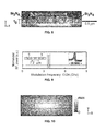
- FIG. 8 provides a view of the net result, based on a cross-sectional scanning electron microscope (SEM) image. Indicated in the figure are the width b 0 and thickness c 0 of the silicon optical waveguide and the thickness to of the nitride layer. The scale bar in the figure represents a distance of 0.5 ⁇ m.
- the wafer was patterned again, and then the phononic crystal structure was formed by using an SF6-based RIE process in an Applied Materials eMxP+ chamber to etch the holes in the nitride layer.
- a concentrated 49% HF solution with surfactant was used to release the membrane by etching away the buried oxide layer.
- the phononic crystal membrane holes also serve as release ports to allow the HF solution access to the buried oxide layer.
- FIG. 16 provides a view, based on a top-down SEM image, of a portion of the resulting structure. Indicated in the figure are the defect size W 0 , defined as the center-to-center distance between the inclusions on either side of the silicon optical waveguide, the lattice constant a 0 , and the hole radius r 0 .
- the scale bar in the figure represents a distance of 5 ⁇ m.
- Facets for fiber access were then obtained by patterning resist with a 1 ⁇ mask in a SUSS MA-6 contact aligner and etching by a deep-RIE process.
- the oxide under-cladding was then removed with a 49% HF etch.
- the etch was timed to remove a vertical thickness of oxide extending down to the underlying silicon, so as to maximize the optical isolation of the waveguide from the substrate. Because an isotropic etch was used, a comparable amount of lateral etch also occurred during the release process. It is significant in this regard that HF etches buried oxide at a rate at least fifty times the rate at which it etches silicon nitride.
- PPER platforms were fabricated as described above.
- the dimensions were:
- a single-wavelength laser line at 1547 nm was intensity-modulated, using a Mach-Zehnder modulator, to synthesize pump waves E 1 a ( ⁇ 1 ) and E 2 a ( ⁇ 2 ) (equivalently, a pump wave and a local oscillator wave, as described above) for injection into Wg-A.
- the carrier-frequency component was suppressed by optimizing the bias voltage, so that only the two sidebands were injected into the waveguide.
- the phonon supermodes generated the new signal field E s b ( ⁇ s ) through travelling-wave phase modulation of the probe wave E 3 b ( ⁇ 3 ), which was injected into Wg-B at a wavelength of 1536 nm.
- the beat signal between the interfering pump waves was thus coherently transferred from Wg-A to Wg-B.
- the transduced signal was then measured at the output of Wg-B through heterodyne detection.
- the frequency of the excited phonon was controlled by changing the RF modulation frequency ⁇ . Sweeping the modulation frequency enabled quantitative study of the frequency response of the dual-channel PPER system from 1-9 GHz.
- a portion of the 1536-nm probe beam was split off to provide a local oscillator and passed through an acousto-optic modulator with a frequency shift ( ⁇ /2 ⁇ ) of 40 MHz. It was then combined with the main (phonon-modulated) probe beam using a directional coupler. The beat note between local oscillator ( ⁇ 3 + ⁇ ) and the main probe beam ( ⁇ 3 ⁇ ) was analysed with an RF spectrum analyser. An estimated fiber-to-chip coupling loss of 15 dB and waveguide propagation loss of ⁇ 1 dB cm ⁇ 1 were found through waveguide cutback measurements. The internal powers of the pump and probe beams were 7 mW and 6.3 mW, respectively.
- FIG. 17 is a schematic diagram of the apparatus used to measure the Brillouin nonlinearities of PnC-BAM waveguides in experiments that are reported here.
- the legends in the figure have the following meanings: Pump: 1,547 nm laser; Probe: 1,536 nm laser, IM: intensity modulator; RF: RF generator for the intensity modulator; AOM: acousto-optical modulator; IF: interference filter; PD: fast speed photodiode receivers; SA: spectrum analyser.
- FIG. 18 provides a plot of the normalized RF response of the example PPER system.
- the solid curve represents experimental measurements, and the broken curve represents the theoretical prediction based on a second-order transfer function.
- the system noise floor is also indicated in the figure.
- the measured second-order response exhibits a very large out-of-band rejection of >70 dB; this implies that optical cross-talk will pose no limitation to the dynamic range of the measured frequency response.
- the contrast of the measurements is limited only by the measurement noise floor, which is indicated in the figure.
- the PPER response is determined solely by phonon supermodes straddling both waveguides. These supermodes are controllable by engineering the PnC structure. For example, the center frequencies of PPER supermodes can be tailored by engineering the defect size W o .
- FIG. 19 provides two plots of the measured and normalized RF response, i.e. the emit-receive response, of a PPER system as a function of frequency.
- the two plots compare the effect of changing the defect size W o .
- the PPER transfer function can also be shaped by lithographically controlling N, N c and W o to control the frequency splitting and decay rate of the PnC supermodes.
- N, N c and W o to control the frequency splitting and decay rate of the PnC supermodes.
- FIG. 20 in the main view, provides a plot of the coupling rate ⁇ versus the reciprocal of the net decay rate ⁇ net ⁇ 1 extracted from measured RF responses of four PPER systems having different sets of design parameters, which are described below. Results are shown in log-log scale. The inset in the top-left corner of the plot is the schematic geometry of the BAM waveguides.
- insets i-IV the experimentally measured and normalized RF responses of example PPER devices as a function of frequency.
- the design values ⁇ N, N c , N ⁇ are varied among the insets as follows; Inset I: ⁇ 6, 6, 6 ⁇ ; Inset II: ⁇ 6, 4, 6 ⁇ ; Inset III: ⁇ 4, 4, 4 ⁇ ; Inset IV: ⁇ 2, 2, 2 ⁇ .
- this compound emit-receive system behaves as a two-port (in the present example) optical system with negligible optical cross-talk and back-reflection: Information is transferred from one port to another through phononic information transduction. As this travelling-wave (or reflectionless) geometry negates the need for optical isolators, this platform is directly compatible with silicon-photonic systems.
- this hybrid photonic-phononic emit-receive approach yields filter shapes and frequency that do not change, even as the optical power is varied by orders of magnitude. This approach negates the need for frequency stabilization (or frequency locking), which often limits the practical utility of resonant optical filtering.
- DBR distributed Bragg reflector
- a waveguide with a short-period corrugation will allow light to propagate at a frequency below the photonic stopband.
- the period can be slowly increased so that the stopband is shifted downward to the optical frequency.
- a long-period corrugation can be designed to permit propagation at optical frequencies above the stopband, and the corrugations can have a shorter period in the mirror regions so as to shift the stopband upward.
- FIG. 21 shows a corrugated optical waveguide 200 in which there are gradual transitions 205 , 210 (not shown explicitly) between short-period corrugation region 220 and long-period corrugation regions 225 , 230 .
- long-period region 225 is made relatively short, it can serve as a partially reflective optical coupling region.
- long-period region 230 is made relatively long, it can serve as the strongly reflective end-stop region.
- light can resonate at frequencies below the photonic stopband.
- Fabry-Perot cavity not only to the emitter waveguide, but also to the receiver waveguide to increase the efficiency of modulation onto the probe wave. Similar tradeoffs between bandwidth and efficiency will be encountered in the receiver waveguide.
- modulation of the optical carrier at frequency ⁇ 2 has given rise to a pair of sidebands, shown in the figure as lying near the center frequency on its left and right sides.
- the RF modulation frequency is less than the beat frequency ⁇ 2 ⁇ 1 that produces the phonons.
- the optical carrier at ⁇ 4 is modulated at a high RF frequency that produces sidebands S ⁇ , S + so far removed from the center frequency that the lower-frequency sideband S. reaches close proximity to ⁇ 2 .
- the distance (in frequency) between ⁇ 2 and the sideband S. is smaller than the distance between ⁇ 1 and ⁇ 2 .
- optical mixing provides a pathway for modulating an optical carrier at an RF frequency of tens, or even hundreds, of gigahertz, and then downshifting the modulation frequency and transducing phonons modulated at the downshifted frequency.
- the effective downshift occurs when, in the example given above, sideband S. interacts as though it were a sideband of the carrier at ⁇ 1 .
- the process is reversed. This can be done so as to modulate the original RF signal onto the optical carrier in the receiver waveguide.
- the PnC structure can be engineered to impart desired characteristics to the transfer function for phononic coupling between waveguides.
- the phononic modal resonance associated with each optical waveguide depends on the width W 0 of the line defect within which the optical waveguide is placed. Even without reliance on waveguide-to-waveguide coupling through the PnC structure, the modal response of an individual line defect can be utilized for purposes such as RF filtering.
- one useful application of the principles described above injects the emitter optical carrier waves into a waveguide, and also injects the receiver optical carrier wave into the same waveguide.
- An RF signal is modulated onto one of the emitter carrier waves. Phonons generated by the beat tone between the emitter carriers are confined within the line defect by the surrounding PnC structure. The generated phonons modulate the RF signal onto the receiver carrier.
- RF filtering takes place because only the phonon frequencies ⁇ that satisfy the conditions for modal resonance in the line defect play a substantial role in the phononic transduction and hence in the modulation onto the receiver carrier wave.
- the emitter and receiver waveguides (and the line defects in which they are placed) are coupled through the PnC structure.
- the response function (viewing the device as a filter) is second order because of the hybridization of the two line defects to form two supermodes.
- Higher-order responses can be produced by adding more line defects to the PnC structure between the two waveguides.
- a third-order filter can be created by adding a third line defect to the midline between the emitter and receiver waveguides.
- FIG. 23 is a schematic diagram providing an example of a multistage filter. As seen in the figure, emitter waveguide 240 and receiver waveguide 245 are embedded in PnC structure 250 . Each waveguide is embedded in a respective line defect region 255 , 260 . A plurality (two, in this non-limiting example) of additional line defect regions 265 , 270 is interposed between the emitter and receiver waveguides.
- phase delays can be achieved by coupling continuous-wave signals from the RF domain to the optical domain to the acoustic domain and back, and time delays can be achieved by similar coupling of pulsed signals.
Abstract
Description
Claims (23)
Priority Applications (1)
| Application Number | Priority Date | Filing Date | Title |
|---|---|---|---|
| US15/060,388 US9696492B1 (en) | 2016-03-03 | 2016-03-03 | On-chip photonic-phononic emitter-receiver apparatus |
Applications Claiming Priority (1)
| Application Number | Priority Date | Filing Date | Title |
|---|---|---|---|
| US15/060,388 US9696492B1 (en) | 2016-03-03 | 2016-03-03 | On-chip photonic-phononic emitter-receiver apparatus |
Publications (1)
| Publication Number | Publication Date |
|---|---|
| US9696492B1 true US9696492B1 (en) | 2017-07-04 |
Family
ID=59152399
Family Applications (1)
| Application Number | Title | Priority Date | Filing Date |
|---|---|---|---|
| US15/060,388 Active US9696492B1 (en) | 2016-03-03 | 2016-03-03 | On-chip photonic-phononic emitter-receiver apparatus |
Country Status (1)
| Country | Link |
|---|---|
| US (1) | US9696492B1 (en) |
Cited By (18)
| Publication number | Priority date | Publication date | Assignee | Title |
|---|---|---|---|---|
| US20180063745A1 (en) * | 2016-07-16 | 2018-03-01 | GenXComm, Inc. | Interference cancellation methods and apparatus |
| US20180067182A1 (en) * | 2016-09-06 | 2018-03-08 | The Royal Institution For The Advancement Of Learning/Mcgill University | Topologically-protected traveling-wave amplifier |
| CN108859594A (en) * | 2018-04-26 | 2018-11-23 | 华东交通大学 | A kind of High Speed Railway Trains wheel vibration absorber based on phonon crystal |
| CN109038211A (en) * | 2018-08-14 | 2018-12-18 | 华中科技大学 | A kind of laser light source based on acousto-optic interaction |
| US10281333B2 (en) * | 2016-06-13 | 2019-05-07 | Panasonic Intellectual Property Management Co., Ltd. | Infrared sensor |
| US20190178718A1 (en) * | 2017-12-11 | 2019-06-13 | Panasonic Intellectual Property Management Co., Ltd. | Infrared sensor and method for cooling bolometer infrared ray receiver of infrared sensor |
| US10367584B2 (en) | 2016-07-29 | 2019-07-30 | PSquared Technologies LLC | Electro-mechanic-photonic delay line for analog signal processing |
| CN110954512A (en) * | 2019-10-18 | 2020-04-03 | 北京应用物理与计算数学研究所 | Analytic calculation method and device for phonon spectrum of primitive cell of alloy material |
| US11150409B2 (en) | 2018-12-27 | 2021-10-19 | GenXComm, Inc. | Saw assisted facet etch dicing |
| US11163114B2 (en) * | 2019-08-23 | 2021-11-02 | Globalfoundries U.S. Inc. | Waveguide structures |
| US11215755B2 (en) | 2019-09-19 | 2022-01-04 | GenXComm, Inc. | Low loss, polarization-independent, large bandwidth mode converter for edge coupling |
| US11309965B2 (en) | 2019-07-15 | 2022-04-19 | GenXComm, Inc. | Efficiently combining multiple taps of an optical filter |
| US11378741B2 (en) * | 2018-08-10 | 2022-07-05 | Yale University | Opto-acoustic signal processing |
| WO2022178589A1 (en) * | 2021-02-24 | 2022-09-01 | The University Of Queensland | Phononic circuit components |
| US11469821B2 (en) | 2015-12-13 | 2022-10-11 | GenXComm, Inc. | Interference cancellation methods and apparatus |
| US11539394B2 (en) | 2019-10-29 | 2022-12-27 | GenXComm, Inc. | Self-interference mitigation in in-band full-duplex communication systems |
| US11796737B2 (en) | 2020-08-10 | 2023-10-24 | GenXComm, Inc. | Co-manufacturing of silicon-on-insulator waveguides and silicon nitride waveguides for hybrid photonic integrated circuits |
| US11838056B2 (en) | 2021-10-25 | 2023-12-05 | GenXComm, Inc. | Hybrid photonic integrated circuits for ultra-low phase noise signal generators |
Citations (5)
| Publication number | Priority date | Publication date | Assignee | Title |
|---|---|---|---|---|
| US20050259937A1 (en) * | 2004-03-26 | 2005-11-24 | Whaley Ralph D Jr | Low optical overlap mode (LOOM) waveguiding system and method of making same |
| US7421179B1 (en) * | 2006-09-29 | 2008-09-02 | Wei Jiang | Apparatus and method for switching, modulation and dynamic control of light transmission using photonic crystals |
| US20100226608A1 (en) * | 2008-08-28 | 2010-09-09 | Board Of Regents, The University Of Texas System | Multimode interference coupler for use with slot photonic crystal waveguides |
| US8600200B1 (en) | 2010-04-01 | 2013-12-03 | Sandia Corporation | Nano-optomechanical transducer |
| US9268092B1 (en) | 2013-03-14 | 2016-02-23 | Sandia Corporation | Guided wave opto-acoustic device |
-
2016
- 2016-03-03 US US15/060,388 patent/US9696492B1/en active Active
Patent Citations (5)
| Publication number | Priority date | Publication date | Assignee | Title |
|---|---|---|---|---|
| US20050259937A1 (en) * | 2004-03-26 | 2005-11-24 | Whaley Ralph D Jr | Low optical overlap mode (LOOM) waveguiding system and method of making same |
| US7421179B1 (en) * | 2006-09-29 | 2008-09-02 | Wei Jiang | Apparatus and method for switching, modulation and dynamic control of light transmission using photonic crystals |
| US20100226608A1 (en) * | 2008-08-28 | 2010-09-09 | Board Of Regents, The University Of Texas System | Multimode interference coupler for use with slot photonic crystal waveguides |
| US8600200B1 (en) | 2010-04-01 | 2013-12-03 | Sandia Corporation | Nano-optomechanical transducer |
| US9268092B1 (en) | 2013-03-14 | 2016-02-23 | Sandia Corporation | Guided wave opto-acoustic device |
Non-Patent Citations (8)
| Title |
|---|
| "Analyses of mode coupling in joined parallel phononic crystal waveguides" by Sun et al, Physical Review B, vol. 71, paper 174303, 2005. * |
| "Confined longitudinal acoustic phonon modes in free-standing Si membranes coherently excited by femtosecond laser pulses" by Hudert et al, Physical Review B, vol. 79, paper 201307, 2009. * |
| "General recipe for designing photonic crystal cavities" by Englund et al, Optics Express, vol. 13, No. 6, pp. 5961-5975, 2005. * |
| "Microwave synthesizer using an on-chip Brillouin oscillator" by Li et al, Nature Communications, vol. 4:2097, pp. 1-7, Jun. 2013. * |
| "Photon confinement in photonic crystal nanocavities" by Lalanne et al, Laser & Photonics Review, vol. 2, No. 6, pp. 514-526, 2008. * |
| Rakich, P. T. et al., "Giant Enhancement of Stimulated Brillouin Scattering in the Subwavelength Limit" 2012, article 011008. |
| Shin, H. et al., "Control of Coherent Information Via On-Chip Photonic-Phononic Emitter-Receivers", Nature Communications, 2015, article DOI: 10.1038/nmcomms7427. |
| Shin, H. et al., "Tailorable Stimulated Brillouin Scattering in Nanoscale Silicon Waveguides", Nature Communications, 2013, article DOI 10.1038/nmcomms2943. |
Cited By (33)
| Publication number | Priority date | Publication date | Assignee | Title |
|---|---|---|---|---|
| US11469821B2 (en) | 2015-12-13 | 2022-10-11 | GenXComm, Inc. | Interference cancellation methods and apparatus |
| US10634561B2 (en) * | 2016-06-13 | 2020-04-28 | Panasonic Intellectual Property Management Co., Ltd. | Thin film and method of using the same |
| US10281333B2 (en) * | 2016-06-13 | 2019-05-07 | Panasonic Intellectual Property Management Co., Ltd. | Infrared sensor |
| US20190293490A1 (en) * | 2016-06-13 | 2019-09-26 | Panasonic Intellectual Property Management Co., Ltd. | Infrared sensor |
| US11330464B2 (en) * | 2016-07-16 | 2022-05-10 | GenXComm, Inc. | Interference cancellation methods and apparatus |
| US11032737B2 (en) * | 2016-07-16 | 2021-06-08 | GenXComm, Inc. | Interference cancellation methods and apparatus |
| US10257746B2 (en) * | 2016-07-16 | 2019-04-09 | GenXComm, Inc. | Interference cancellation methods and apparatus |
| US10321357B1 (en) * | 2016-07-16 | 2019-06-11 | GenXComm, Inc. | Interference cancellation methods and apparatus |
| US10873877B2 (en) * | 2016-07-16 | 2020-12-22 | GenXComm, Inc. | Interference cancellation methods and apparatus |
| US20180063745A1 (en) * | 2016-07-16 | 2018-03-01 | GenXComm, Inc. | Interference cancellation methods and apparatus |
| US20190253922A1 (en) * | 2016-07-16 | 2019-08-15 | GenXComm, Inc. | Interference cancellation methods and apparatus |
| US10367584B2 (en) | 2016-07-29 | 2019-07-30 | PSquared Technologies LLC | Electro-mechanic-photonic delay line for analog signal processing |
| US20180067182A1 (en) * | 2016-09-06 | 2018-03-08 | The Royal Institution For The Advancement Of Learning/Mcgill University | Topologically-protected traveling-wave amplifier |
| US10725131B2 (en) * | 2016-09-06 | 2020-07-28 | The Royal Institution For The Advancement Of Learning/Mcgill University | Topologically-protected traveling-wave amplifier |
| US10605667B2 (en) * | 2017-12-11 | 2020-03-31 | Panasonic Intellectual Property Management Co., Ltd. | Infrared sensor and method for cooling bolometer infrared ray receiver of infrared sensor |
| US11320313B2 (en) | 2017-12-11 | 2022-05-03 | Panasonic intellectual property Management co., Ltd | Infrared sensor and method for cooling bolometer infrared ray receiver of infrared sensor |
| US20190178718A1 (en) * | 2017-12-11 | 2019-06-13 | Panasonic Intellectual Property Management Co., Ltd. | Infrared sensor and method for cooling bolometer infrared ray receiver of infrared sensor |
| CN108859594B (en) * | 2018-04-26 | 2021-09-28 | 华东交通大学 | High-speed railway train wheel bump leveller based on phononic crystal |
| CN108859594A (en) * | 2018-04-26 | 2018-11-23 | 华东交通大学 | A kind of High Speed Railway Trains wheel vibration absorber based on phonon crystal |
| US11378741B2 (en) * | 2018-08-10 | 2022-07-05 | Yale University | Opto-acoustic signal processing |
| CN109038211A (en) * | 2018-08-14 | 2018-12-18 | 华中科技大学 | A kind of laser light source based on acousto-optic interaction |
| CN109038211B (en) * | 2018-08-14 | 2020-05-19 | 华中科技大学 | Laser light source based on acousto-optic interaction |
| US11150409B2 (en) | 2018-12-27 | 2021-10-19 | GenXComm, Inc. | Saw assisted facet etch dicing |
| US11309965B2 (en) | 2019-07-15 | 2022-04-19 | GenXComm, Inc. | Efficiently combining multiple taps of an optical filter |
| US11163114B2 (en) * | 2019-08-23 | 2021-11-02 | Globalfoundries U.S. Inc. | Waveguide structures |
| US20210396929A1 (en) * | 2019-08-23 | 2021-12-23 | Globalfoundries U.S. Inc. | Waveguide structures |
| US11822122B2 (en) * | 2019-08-23 | 2023-11-21 | Globalfoundries U.S. Inc. | Waveguide structures |
| US11215755B2 (en) | 2019-09-19 | 2022-01-04 | GenXComm, Inc. | Low loss, polarization-independent, large bandwidth mode converter for edge coupling |
| CN110954512A (en) * | 2019-10-18 | 2020-04-03 | 北京应用物理与计算数学研究所 | Analytic calculation method and device for phonon spectrum of primitive cell of alloy material |
| US11539394B2 (en) | 2019-10-29 | 2022-12-27 | GenXComm, Inc. | Self-interference mitigation in in-band full-duplex communication systems |
| US11796737B2 (en) | 2020-08-10 | 2023-10-24 | GenXComm, Inc. | Co-manufacturing of silicon-on-insulator waveguides and silicon nitride waveguides for hybrid photonic integrated circuits |
| WO2022178589A1 (en) * | 2021-02-24 | 2022-09-01 | The University Of Queensland | Phononic circuit components |
| US11838056B2 (en) | 2021-10-25 | 2023-12-05 | GenXComm, Inc. | Hybrid photonic integrated circuits for ultra-low phase noise signal generators |
Similar Documents
| Publication | Publication Date | Title |
|---|---|---|
| US9696492B1 (en) | On-chip photonic-phononic emitter-receiver apparatus | |
| US10025123B1 (en) | Guided wave opto-acoustic device | |
| US10254478B2 (en) | Integrated impedance-matched photonic zero-index metamaterials | |
| Hagness et al. | FDTD microcavity simulations: design and experimental realization of waveguide-coupled single-mode ring and whispering-gallery-mode disk resonators | |
| KR100739522B1 (en) | Electromagnetic wave frequency filter | |
| US6947632B2 (en) | Method of implementing the kerr effect in an integrated ring resonator (the kerr integrated optical ring filter) to achieve all-optical wavelength switching, as well as all-optical tunable filtering, add-and -drop multiplexing, space switching and optical intensity modulation | |
| Tanaka et al. | Coupling properties in a 2-D photonic crystal slab directional coupler with a triangular lattice of air holes | |
| US6804446B1 (en) | Waveguide including at least one photonic crystal region for directing signals propagating therethrough | |
| Pan et al. | Experimental demonstration of an all-optical analogue to the superradiance effect in an on-chip photonic crystal resonator system | |
| Nguyen et al. | Lateral leakage in silicon photonics: theory, applications, and future directions | |
| Ghosh et al. | Laterally vibrating resonator based elasto-optic modulation in aluminum nitride | |
| Mookherjea | Using gain to tune the dispersion relation of coupled-resonator optical waveguides | |
| US9057891B2 (en) | Nonlinear frequency conversion in nanoslab optical waveguides | |
| US7110641B2 (en) | Device for directional and wavelength-selective optical coupling | |
| Bianki et al. | Mutlilayer wedge disks CROW for an optical delay line | |
| Jen et al. | Backward collinear guided-wave-acousto-optic interactions in single-mode fibers | |
| US9671673B2 (en) | Optical device for dispersion compensation | |
| Yamada et al. | Silicon wire waveguiding system: fundamental characteristics and applications | |
| Sharkawy et al. | Analysis and applications of photonic crystals coupled waveguide theory | |
| Yücel | Coupling of Photonic Crystal Surface Modes | |
| Mahmoud et al. | Electro-optically controlled acousto-optic racetrack modulator etched in LNOI platform | |
| Pu et al. | AlGaAs-on-insulator nonlinear photonics | |
| Liu et al. | Design of free-standing GaN strip waveguide and grating couplers | |
| Rey | Active slow light in silicon photonic crystals: tunable delay and Raman gain | |
| Mendez-Astudillo et al. | Phase-shifted multimode bragg gratings in silicon-on-insulator for sensing applications |
Legal Events
| Date | Code | Title | Description |
|---|---|---|---|
| AS | Assignment |
Owner name: U.S. DEPARTMENT OF ENERGY, DISTRICT OF COLUMBIA Free format text: CONFIRMATORY LICENSE;ASSIGNOR:SANDIA CORPORATION;REEL/FRAME:039166/0721 Effective date: 20160528 |
|
| AS | Assignment |
Owner name: SANDIA CORPORATION, NEW MEXICO Free format text: ASSIGNMENT OF ASSIGNORS INTEREST;ASSIGNORS:JARECKI, ROBERT L., JR;SIDDIQUI, ALEEM;STARBUCK, ANDREW LEA;REEL/FRAME:040713/0345 Effective date: 20160803 |
|
| STCF | Information on status: patent grant |
Free format text: PATENTED CASE |
|
| AS | Assignment |
Owner name: NATIONAL TECHNOLOGY & ENGINEERING SOLUTIONS OF SAN Free format text: CHANGE OF NAME;ASSIGNOR:SANDIA CORPORATION;REEL/FRAME:043618/0610 Effective date: 20170501 |
|
| AS | Assignment |
Owner name: NATIONAL TECHNOLOGY & ENGINEERING SOLUTIONS OF SANDIA, LLC, NEW MEXICO Free format text: ASSIGNMENT OF ASSIGNORS INTEREST;ASSIGNOR:COX, JONATHAN;REEL/FRAME:052356/0152 Effective date: 20111017 |
|
| MAFP | Maintenance fee payment |
Free format text: PAYMENT OF MAINTENANCE FEE, 4TH YEAR, LARGE ENTITY (ORIGINAL EVENT CODE: M1551); ENTITY STATUS OF PATENT OWNER: LARGE ENTITY Year of fee payment: 4 |