US9690505B2 - Refresh row address - Google Patents

Refresh row address Download PDF

Info

Publication number
US9690505B2
US9690505B2 US14/912,502 US201314912502A US9690505B2 US 9690505 B2 US9690505 B2 US 9690505B2 US 201314912502 A US201314912502 A US 201314912502A US 9690505 B2 US9690505 B2 US 9690505B2
Authority
US
United States
Prior art keywords
row address
counter
row
activated
lru
Prior art date
Legal status (The legal status is an assumption and is not a legal conclusion. Google has not performed a legal analysis and makes no representation as to the accuracy of the status listed.)
Active
Application number
US14/912,502
Other versions
US20160202926A1 (en
Inventor
Melvin K. Benedict
Current Assignee (The listed assignees may be inaccurate. Google has not performed a legal analysis and makes no representation or warranty as to the accuracy of the list.)
Hewlett Packard Enterprise Development LP
Original Assignee
Hewlett Packard Enterprise Development LP
Priority date (The priority date is an assumption and is not a legal conclusion. Google has not performed a legal analysis and makes no representation as to the accuracy of the date listed.)
Filing date
Publication date
Application filed by Hewlett Packard Enterprise Development LP filed Critical Hewlett Packard Enterprise Development LP
Assigned to HEWLETT-PACKARD DEVELOPMENT COMPANY, L.P. reassignment HEWLETT-PACKARD DEVELOPMENT COMPANY, L.P. ASSIGNMENT OF ASSIGNORS INTEREST (SEE DOCUMENT FOR DETAILS). Assignors: BENEDICT, MELVIN K.
Assigned to HEWLETT PACKARD ENTERPRISE DEVELOPMENT LP reassignment HEWLETT PACKARD ENTERPRISE DEVELOPMENT LP ASSIGNMENT OF ASSIGNORS INTEREST (SEE DOCUMENT FOR DETAILS). Assignors: HEWLETT-PACKARD DEVELOPMENT COMPANY, L.P.
Publication of US20160202926A1 publication Critical patent/US20160202926A1/en
Application granted granted Critical
Publication of US9690505B2 publication Critical patent/US9690505B2/en
Active legal-status Critical Current
Anticipated expiration legal-status Critical

Links

Images

Classifications

    • GPHYSICS
    • G06COMPUTING; CALCULATING OR COUNTING
    • G06FELECTRIC DIGITAL DATA PROCESSING
    • G06F3/00Input arrangements for transferring data to be processed into a form capable of being handled by the computer; Output arrangements for transferring data from processing unit to output unit, e.g. interface arrangements
    • G06F3/06Digital input from, or digital output to, record carriers, e.g. RAID, emulated record carriers or networked record carriers
    • G06F3/0601Interfaces specially adapted for storage systems
    • G06F3/0602Interfaces specially adapted for storage systems specifically adapted to achieve a particular effect
    • G06F3/0614Improving the reliability of storage systems
    • G06F3/0619Improving the reliability of storage systems in relation to data integrity, e.g. data losses, bit errors
    • GPHYSICS
    • G11INFORMATION STORAGE
    • G11CSTATIC STORES
    • G11C11/00Digital stores characterised by the use of particular electric or magnetic storage elements; Storage elements therefor
    • G11C11/21Digital stores characterised by the use of particular electric or magnetic storage elements; Storage elements therefor using electric elements
    • G11C11/34Digital stores characterised by the use of particular electric or magnetic storage elements; Storage elements therefor using electric elements using semiconductor devices
    • G11C11/40Digital stores characterised by the use of particular electric or magnetic storage elements; Storage elements therefor using electric elements using semiconductor devices using transistors
    • G11C11/401Digital stores characterised by the use of particular electric or magnetic storage elements; Storage elements therefor using electric elements using semiconductor devices using transistors forming cells needing refreshing or charge regeneration, i.e. dynamic cells
    • G11C11/4063Auxiliary circuits, e.g. for addressing, decoding, driving, writing, sensing or timing
    • G11C11/407Auxiliary circuits, e.g. for addressing, decoding, driving, writing, sensing or timing for memory cells of the field-effect type
    • G11C11/408Address circuits
    • GPHYSICS
    • G06COMPUTING; CALCULATING OR COUNTING
    • G06FELECTRIC DIGITAL DATA PROCESSING
    • G06F12/00Accessing, addressing or allocating within memory systems or architectures
    • G06F12/02Addressing or allocation; Relocation
    • G06F12/08Addressing or allocation; Relocation in hierarchically structured memory systems, e.g. virtual memory systems
    • G06F12/12Replacement control
    • G06F12/121Replacement control using replacement algorithms
    • G06F12/123Replacement control using replacement algorithms with age lists, e.g. queue, most recently used [MRU] list or least recently used [LRU] list
    • GPHYSICS
    • G06COMPUTING; CALCULATING OR COUNTING
    • G06FELECTRIC DIGITAL DATA PROCESSING
    • G06F3/00Input arrangements for transferring data to be processed into a form capable of being handled by the computer; Output arrangements for transferring data from processing unit to output unit, e.g. interface arrangements
    • G06F3/06Digital input from, or digital output to, record carriers, e.g. RAID, emulated record carriers or networked record carriers
    • G06F3/0601Interfaces specially adapted for storage systems
    • G06F3/0628Interfaces specially adapted for storage systems making use of a particular technique
    • G06F3/0653Monitoring storage devices or systems
    • GPHYSICS
    • G06COMPUTING; CALCULATING OR COUNTING
    • G06FELECTRIC DIGITAL DATA PROCESSING
    • G06F3/00Input arrangements for transferring data to be processed into a form capable of being handled by the computer; Output arrangements for transferring data from processing unit to output unit, e.g. interface arrangements
    • G06F3/06Digital input from, or digital output to, record carriers, e.g. RAID, emulated record carriers or networked record carriers
    • G06F3/0601Interfaces specially adapted for storage systems
    • G06F3/0668Interfaces specially adapted for storage systems adopting a particular infrastructure
    • G06F3/0671In-line storage system
    • G06F3/0673Single storage device
    • GPHYSICS
    • G11INFORMATION STORAGE
    • G11CSTATIC STORES
    • G11C11/00Digital stores characterised by the use of particular electric or magnetic storage elements; Storage elements therefor
    • G11C11/21Digital stores characterised by the use of particular electric or magnetic storage elements; Storage elements therefor using electric elements
    • G11C11/34Digital stores characterised by the use of particular electric or magnetic storage elements; Storage elements therefor using electric elements using semiconductor devices
    • G11C11/40Digital stores characterised by the use of particular electric or magnetic storage elements; Storage elements therefor using electric elements using semiconductor devices using transistors
    • G11C11/401Digital stores characterised by the use of particular electric or magnetic storage elements; Storage elements therefor using electric elements using semiconductor devices using transistors forming cells needing refreshing or charge regeneration, i.e. dynamic cells
    • G11C11/406Management or control of the refreshing or charge-regeneration cycles
    • G11C11/40611External triggering or timing of internal or partially internal refresh operations, e.g. auto-refresh or CAS-before-RAS triggered refresh
    • GPHYSICS
    • G11INFORMATION STORAGE
    • G11CSTATIC STORES
    • G11C7/00Arrangements for writing information into, or reading information out from, a digital store
    • G11C7/02Arrangements for writing information into, or reading information out from, a digital store with means for avoiding parasitic signals
    • GPHYSICS
    • G06COMPUTING; CALCULATING OR COUNTING
    • G06FELECTRIC DIGITAL DATA PROCESSING
    • G06F12/00Accessing, addressing or allocating within memory systems or architectures
    • G06F12/02Addressing or allocation; Relocation
    • G06F12/08Addressing or allocation; Relocation in hierarchically structured memory systems, e.g. virtual memory systems
    • G06F12/12Replacement control
    • G06F2212/69
    • GPHYSICS
    • G11INFORMATION STORAGE
    • G11CSTATIC STORES
    • G11C2211/00Indexing scheme relating to digital stores characterized by the use of particular electric or magnetic storage elements; Storage elements therefor
    • G11C2211/401Indexing scheme relating to cells needing refreshing or charge regeneration, i.e. dynamic cells
    • G11C2211/406Refreshing of dynamic cells
    • G11C2211/4065Low level details of refresh operations

Definitions

  • a memory may receive commands to access a memory location of the memory.
  • a Dynamic random access memory may receive an activate command to open a row address of the DRAM to a read or write operation.
  • Manufacturers, vendors and/or suppliers are challenged to provide users with more accurate methods for ensuring that data at the memory is not corrupted.
  • FIG. 2 is another example block diagram of a device to refresh a row address if a counter threshold is exceeded
  • FIG. 3 is an example block diagram of a computing device including instructions for refreshing a row address if a counter threshold is exceeded;
  • Each of the counters may correspond to one of the row addresses of the table.
  • the row unit may determine if an activated row address of the memory is included in the table.
  • the counter unit may increment at least one of the first counter of the first row address and the second counter of the second row address, if the activated row address is not included in the table.
  • the refresh unit may refresh at least one of the first and second row addresses if at least one of the first and second counters exceeds a counter threshold. At least one the first and second row addresses may be adjacent to the activated row address.
  • the counter unit 120 may increment a first counter 122 - 1 of a first row address 112 - 1 included in the table 110 , if the activated row address is not included in the table 110 .
  • the counter unit 120 may increment a second counter 122 - 2 of a second row address 112 - 2 included in the table 110 , if the activated row address is not included in the table 110 .
  • the counter unit 120 may increment each of the first and second counters 122 - 1 and 122 - 2 by a single unit.
  • first counter 122 - 1 may be incremented from 29 to 30 or the second counter 122 - 2 may be incremented from 188 to 189.
  • the first and second row addresses 112 - 1 and 112 - 2 may be victim row addresses.
  • the refresh unit 150 may refresh at least one of the first and second row addresses 112 - 1 and 112 - 2 if at least one of the first and second counters 122 - 1 and 122 - 2 exceeds a counter threshold 152 .
  • the refresh unit 150 may refresh the first row address 112 - 1 if the first counter 122 - 1 exceeds the counter threshold 152 .
  • the refresh unit 150 may refresh the second row address 112 - 2 if the second counter 122 - 2 exceeds the counter threshold 152 .
  • a value of the counter threshold 152 may be determined experimentally and/or based on a property of the memory. In one instance, the counter threshold 152 may be approximately 300.
  • the counter unit 120 may add the first and/or second row addresses 112 - 1 and 112 - 2 to the table 110 in order to carry out the above counting, if the table 110 does not already include the first and/or second row addresses 112 - 1 and 112 - 2 and the activated row address is not included in the table 110 .
  • the counters 122 for these newly added row addresses 112 may be set to the minimum value or the like.
  • the LRU unit 210 may set a first LRU field 212 - 1 of the first row address 112 - 1 and a second LRU field 212 - 2 of the second row address 112 - 2 to a maximum value, if the activated row address is not included in the table 110 .
  • the maximum value may depend on a size of the table 110 . For example, if the table 110 may hold a maximum of 16 row addresses 112 , the maximum value may be 15 or 16.
  • the LRU unit 210 may also decrement all of the LRU fields 212 - 1 to 212 - n each time a row address of the memory 250 is to be activated, such as after setting the first, second and/or third LRU fields 212 - 1 to 212 - 3 .
  • the replacement unit 220 may replace the row address 112 of the table 110 having the a replacement status 222 that is set with at least one of the first and second row addresses 112 - 1 and 112 - 2 , if the table 110 is full and replacement 220 seeks to add at least one of the first and second row addresses 112 - 1 and 112 - 2 to the table 110 . For instance, if two row addresses 112 are to be added and the table 110 is full, two row addresses having the set replacement status 222 may be replaced, with the LRU unit 210 to determine which of the row addresses 112 with the LRU field 212 less than the minimum value has a lowest value for its counter 122 .
  • All of the plurality of counters 122 - 1 to 122 - n and the LRU fields 212 - 1 to 212 - n may be reset at an end of a refresh interval 240 .
  • the refresh interval 240 may be a interval that, for example, is determined experimentally or set based on characteristics of the memory 250 . For example, if the refresh interval 240 is 64 milliseconds (ms), the LRU unit 210 may reset all of the LRU fields 212 - 1 to 212 - n to a default value, such as 0 or 1, every 64 ms. Similarly, the counter unit 120 may reset all of the counters 122 - 1 to 122 - n to the default value, every 64 ms.
  • FIG. 3 is an example block diagram of a computing device 300 including instructions for refreshing a row address if a counter threshold is exceeded.
  • the computing device 300 includes a processor 310 and a machine-readable storage medium 320 .
  • the machine-readable storage medium 320 further includes instructions 322 , 324 , 326 and 328 for refreshing a row address if a counter threshold is exceeded.
  • the processor 310 may be, at least one central processing unit (CPU), at least one semiconductor-based microprocessor, at least one graphics processing unit (GPU), a microcontroller, special purpose logic hardware controlled by microcode or other hardware devices suitable for retrieval and execution of instructions stored in the machine-readable storage medium 320 , or combinations thereof.
  • the processor 310 may fetch, decode, and execute instructions 322 , 324 , 326 and 328 to implement refreshing the row address if the counter threshold is exceeded.
  • the processor 310 may include at least one integrated circuit (IC), other control logic, other electronic circuits, or combinations thereof that include a number of electronic components for performing the functionality of instructions 322 , 324 , 326 and 328 .
  • IC integrated circuit
  • the instructions 322 , 324 , 326 and 328 when executed by a processor can cause the processor to perform processes, such as, the process of FIG. 5 .
  • the increment first counter instructions 322 may be executed by the processor 310 to increment a first counter (not shown) of a first row address of a table (not shown), if an activated row address adjacent to the first row address is not included in the table.
  • the refresh first row address instructions 326 may be executed by the processor 310 to refresh the first row address if the first counter exceeds a counter threshold.
  • the refresh second row address instructions 328 may be executed by the processor 310 to refresh the second row address if the second counter exceeds the counter threshold. Additional instructions (not shown) may be executed by the processor 410 to reset the first counter if the first row address is refreshed and to reset the second counter if the second row address is refreshed.
  • the device 100 determines if an activated row address of a memory is included in a table 110 . Then, at block 420 , the device 100 increments a first counter 122 - 1 of a first row address 112 - 1 of the table 110 and/or a second counter 122 - 2 of a second row address 112 - 2 of the table 110 , if the activated row address is not included in the table 110 . Next, at block 430 , the device 100 compares the first and/or second counters 122 - 1 and 122 - 2 to a counter threshold 152 .
  • the device 100 refreshes the first row address 112 - 1 if the first counter 122 - 1 exceeds the counter threshold 152 .
  • the device 100 refreshes the second row address 112 - 2 if the second counter 122 - 2 exceeds the counter threshold 152 .
  • the first and second row addresses 112 - 1 and 112 - 2 are adjacent to the activated row address at the memory.
  • the device 200 determines if the first row address 112 - 1 is included in the table 110 . If the first row address 112 - 1 is included in the table 110 , the method 500 flows to block 510 , where the device 200 increments a first counter 122 - 1 . Then, at block 512 , the device 200 determines if the first counter 122 - 1 exceeds the counter threshold 152 . If the first counter 122 - 1 exceeds the counter threshold 152 , the method 500 flows to point E, as explained in further detail below.
  • the method 500 flows to block 514 , where the device 200 sets a first LRU field 212 - 1 to a maximum value, and then flows to point D.
  • Each of the counters 122 - 1 to 122 - n corresponds to one of the row addresses 112 - 1 to 112 - n and each of the LRU fields 212 - 1 to 212 - n corresponds to one of the row addresses 112 - 1 to 112 - n.
  • the row address 112 having an LRU field 212 below the minimum value and a lowest value for its counter 122 may be selected to be removed.
  • the method 500 flows from block 526 to block 528 .
  • the method 500 similarly flows from block 524 to block 528 , if the table 110 is not full.
  • the device 200 adds the first row address 112 - 1 to the table 110 .
  • the device 200 sets the first LRU 212 - 1 to the maximum value.
  • the method 500 then flows to point D.
  • the method 500 flows from block 534 to block 536 .
  • the method 500 similarly flows from block 532 to block 536 , if the table 110 is not full.
  • the device 200 adds the second row address 112 - 2 to the table 110 .
  • the device 200 sets the second LRU 212 - 2 to the maximum value. The method 500 then flows to point D.
  • FIG. 5D illustrates a process occurring simultaneously with the process shown in FIGS. 5A to 5C .
  • the device 200 determines if a refresh interval 240 has expired. If the refresh interval 240 has expired, the device 200 resets all of the plurality of counters 122 - 1 to 122 - n and all of the plurality of LRU fields 212 - 1 to 212 - n , at block 556 . The method 500 then flows back to block 554 , where the device 200 continues to wait for the next refresh interval 240 to expire.

Landscapes

  • Engineering & Computer Science (AREA)
  • Theoretical Computer Science (AREA)
  • Physics & Mathematics (AREA)
  • General Engineering & Computer Science (AREA)
  • General Physics & Mathematics (AREA)
  • Human Computer Interaction (AREA)
  • Microelectronics & Electronic Packaging (AREA)
  • Computer Hardware Design (AREA)
  • Computer Security & Cryptography (AREA)
  • Memory System Of A Hierarchy Structure (AREA)
  • Dram (AREA)

Abstract

A table may include first and second row addresses that are adjacent an activated row address. A first counter of the first row address may be incremented if the activated row address is not included in the table. A second counter of the second row address may also be incremented if the activated row address is not included in the table. The first row address may be refreshed if the first counter exceeds a counter threshold. The second row address may be refreshed if the second counter exceeds the counter threshold.

Description

BACKGROUND
A memory may receive commands to access a memory location of the memory. For instance, a Dynamic random access memory (DRAM) may receive an activate command to open a row address of the DRAM to a read or write operation. Manufacturers, vendors and/or suppliers are challenged to provide users with more accurate methods for ensuring that data at the memory is not corrupted.
BRIEF DESCRIPTION OF THE DRAWINGS
The following detailed description references the drawings, wherein:
FIG. 1 is an example block diagram of a device to refresh a row address if a counter threshold is exceeded;
FIG. 2 is another example block diagram of a device to refresh a row address if a counter threshold is exceeded;
FIG. 3 is an example block diagram of a computing device including instructions for refreshing a row address if a counter threshold is exceeded;
FIG. 4 is an example flowchart of a method for refreshing a row address if a counter threshold is exceeded; and
FIGS. 5A to 5D is another example flowchart of a method for refreshing a row address if a counter threshold is exceeded.
DETAILED DESCRIPTION
Specific details are given in the following description to provide a thorough understanding of embodiments. However, it will be understood that embodiments may be practiced without these specific details. For example, systems may be shown in block diagrams in order not to obscure embodiments in unnecessary detail. In other instances, well-known processes, structures and techniques may be shown without unnecessary detail in order to avoid obscuring embodiments.
Dynamic random access memory (DRAM) technology and processes have developed to the point where fault mechanisms which were considered second order affects may be fundamental fault mechanisms in today's DRAMs. One such mechanism is known as word-line disturb, which may occur when activate commands are repeatedly issued to a single or small group of row addresses. The activate command may open a row address to a memory access.
These repeated accesses to the same one or more row addresses may affect the contents of physically adjacent word-lines, thus causing silent or soft errors in data stored therein. For example, a sufficiently large number of repeated accesses in a short time may cause electrical or magnetic interference to adjacent physical row addresses, causing one or more bits of a storage element to spontaneously flip to an opposite state. Memory controllers and memories that communicate via a double data rate (DDR) mechanism may allow for a burst of accesses to a same row address during a short time period.
Examples may provide a mechanism for detecting when a either one or two physically adjacent rows of a word-line are being “hammered” or used at a high rate. In turn, a corrective action, such as a refresh, may be triggered to prevent or reduce a likelihood of future data errors to the physically adjacent rows. An example device may include a table, a plurality of counters, a row unit, a counter unit and a refresh unit. The table may store a plurality of row addresses, including first and second row addresses, of a memory. The plurality of counters may include first and second counters.
Each of the counters may correspond to one of the row addresses of the table. The row unit may determine if an activated row address of the memory is included in the table. The counter unit may increment at least one of the first counter of the first row address and the second counter of the second row address, if the activated row address is not included in the table. The refresh unit may refresh at least one of the first and second row addresses if at least one of the first and second counters exceeds a counter threshold. At least one the first and second row addresses may be adjacent to the activated row address.
Thus, examples may prevent data loss by counting adjacent row address activates and taking a corrective action, such as refresh of a victimized row, when the aggressor row is “hammered” or accessed too much. Further, examples may be readily customized to different types of memory array structures without requiring special memory commands.
Referring now to the drawings, FIG. 1 is an example block diagram of a device 100 to refresh a row address if a counter threshold is exceeded. The device 100 may interface with or be included in any type of device including a memory and/or a controller, such as a DRAM, a memory controller, a notebook computer, a desktop computer, an all-in-one system, a server, a network device, a wireless device, a storage device, a mobile device, a thin client, a retail point of sale device, a gaming device, a scientific instrument, and the like.
In FIG. 1, the device 100 is shown to include a table 110, a counter unit 120, a plurality of counters 122-1 to 122-n (where n is a natural number), a row unit 130 and a refresh unit 150. The counter, refresh and row units 120, 150 and 130 may include, for example, a hardware device including electronic circuitry for implementing the functionality described below, such as control logic and/or memory. In addition or as an alternative, the counter, refresh and row units 120, 150 and 130 may be implemented as a series of instructions encoded on a machine-readable storage medium and executable by a processor.
The table 110 and plurality of counters 120-1 to 120-n may include or be stored upon be any electronic, magnetic, optical, or other physical storage device, such as Random Access Memory (RAM), a storage drive, and the like. For example, table 110 and plurality of counters 120-1 to 120-n may be stored on one or more separate memory components, such as registers and/or a single memory device, like a RAM chip. The table 110 may relate to a data structure for arranging information in rows and/or columns. Here, the table 110 may include a plurality of entries, with each entry storing a row address 112. Each of the counters 120 may be a separate locations, either logical or physical, to store a numerical value.
The table 110 may store a plurality of row addresses 112-1 to 112-n of a memory (not shown). For example, a row address may specify a row and/or a row and bank of the memory. Each of the plurality of counters 122-1 to 122-n may correspond to one of the row addresses of the table 110. For example, if the table 110 may hold 16 entries of row addresses 112-1 to 112-16, then there may be 16 counters 122-1 to 122-6, with each counter 122 assigned to one of the entries of the table 110.
The row unit 130 may determine if an activated row address of the memory is included in the table 110. For example, a processor (not shown) may receive a instruction to access the memory, such as for a read or write operation. Then, an activate command may be issued to open a row of the location to be accessed. An address of the row to be opened in response to the activate command may be referred to as the activated row address.
The counter unit 120 may track a number of times at least one of the rows of the memory is next to a row of the memory that is activated, such as by monitoring the row address(es) of the row(s) preceding and/or following the activated row address in the memory. When the activated row address has been accessed at a substantially high rate, the activated row address may be referred to as the hammered row address, and the row addresses adjacent to the activated row address may be referred to as victim row addresses. The table 110 may be used to track the victim row addresses.
For example, the counter unit 120 may increment a first counter 122-1 of a first row address 112-1 included in the table 110, if the activated row address is not included in the table 110. Similarly, the counter unit 120 may increment a second counter 122-2 of a second row address 112-2 included in the table 110, if the activated row address is not included in the table 110. Thus, if the first and second row addresses 112-1 and 112-2 were adjacent to the activated row address and the activated row address was not included in the table 110, the counter unit 120 may increment each of the first and second counters 122-1 and 122-2 by a single unit. For instance, the first counter 122-1 may be incremented from 29 to 30 or the second counter 122-2 may be incremented from 188 to 189. The first and second row addresses 112-1 and 112-2 may be victim row addresses.
The refresh unit 150 may refresh at least one of the first and second row addresses 112-1 and 112-2 if at least one of the first and second counters 122-1 and 122-2 exceeds a counter threshold 152. For example, the refresh unit 150 may refresh the first row address 112-1 if the first counter 122-1 exceeds the counter threshold 152. Also, the refresh unit 150 may refresh the second row address 112-2 if the second counter 122-2 exceeds the counter threshold 152. A value of the counter threshold 152 may be determined experimentally and/or based on a property of the memory. In one instance, the counter threshold 152 may be approximately 300.
Thus, the refresh unit 150 may refresh a victim row address of the table 110 for which one or more adjacent row addresses have been activated numerous times in a time period, such as by more than the counter threshold 150. Further, during this short time period, the victim row address may not have been previously refreshed or activated. The term refresh may refer to a process for preserving the information located at a memory location, such as a row address. A refresh may be carried out numerous ways depending on a memory architecture, such as by a periodic pre-charge, read of and/or rewrite to the memory location.
The counter unit 120 may reset the first counter 122-1 to a minimum value, if the first counter 122-1 exceeds the counter threshold 152. The counter unit 120 may also reset the second counter 122-2 to the minimum value, if the second counter 122-2 exceeds the counter threshold 152. The minimum value may be, for example, 0 or some other low value. Thus, the counter unit 120 may restart a count for a number of times a row address has been victimized after the victimized row is refreshed. Also, the counter unit 120 may add the first and/or second row addresses 112-1 and 112-2 to the table 110 in order to carry out the above counting, if the table 110 does not already include the first and/or second row addresses 112-1 and 112-2 and the activated row address is not included in the table 110. In this case, the counters 122 for these newly added row addresses 112 may be set to the minimum value or the like.
FIG. 2 is another example block diagram of a device 200 to refresh a row address if a counter threshold is exceeded. The device 200 may interface with or be included in any type of device including a memory and/or a controller, such as a DRAM, a memory controller, a notebook computer, a desktop computer, an all-in-one system, a server, a network device, a wireless device, a storage device, a mobile device, a thin client, a retail point of sale device, a gaming device, a scientific instrument, and the like.
Here, the device 200 is shown to interface with a memory 250. While FIG. 2 shows the device 200 to be separate from the memory 250, examples may include the device 200 to be integrated with the memory 250 and/or a memory controller (not shown). Example types of the memory 250 may be Random Access Memory (RAM) like synchronous dynamic random-access memory (SDRAM), dynamic random access memory (DRAM), or graphics RAM. Further example types of the memory 250 may include NAND flash memory and main memory. In addition, the memory 250 may have a double data rate (DDR) interface (not shown). The DDR interface may allow the memory 250 to transfer data on both rising and falling edges of a clock signal along a bus. The DDR interface 252 may include any generation of DDR, such as DDR first generation (DDR1) through DDR fourth generation (DDR4).
The device 200 of FIG. 2 may include the functionality and/or hardware of the device 100 of FIG. 1. For example, the device 200 includes the table 110, the counter unit 120, the plurality of counters 122-1 to 122-n, the row unit 130 and the refresh unit 150. Further, the device 200 includes a least recently used (LRU) unit, a plurality of LRU fields 212-1 to 212-n, a replacement unit 220, a plurality of replacement status fields 222-1 to 222-n and a refresh interval 240.
The LRU and replacement units 210 and 220 may include, for example, a hardware device including electronic circuitry for implementing the functionality described below, such as control logic and/or memory. In addition or as an alternative, the LRU and replacement units 210 and 220 may be implemented as a series of instructions encoded on a machine-readable storage medium and executable by a processor. The plurality of LRU fields 212-1 to 212-n, plurality of replacement status fields 222-1 to 222-n and the refresh interval 240 may include or be stored upon be any electronic, magnetic, optical, or other physical storage device, such as Random Access Memory (RAM), a storage drive, and the like.
The device 200 may receive the activated row address and/or intercept an activate command intended for the row address to be activated from a processor, cache, and/or controller (not shown). As noted above, the first and second counters 122-1 and 122-2 are only incremented if the first and second addresses 112-1 and 112-2 are adjacent to the activated row address and the activated row address is not currently included in the table 110. However, if the activated row address 112-3 is included in the table 110, the counter unit 120 may instead reset a third counter 122-3 of the activated row address 112-3 to the minimum value. In this case, the first and second counters 122-1 and 122-2 are not incremented.
The LRU unit 210 may include any type of policy or algorithm to replace a least recently used row address 112 of the table 110. For example, if the table 110 is full and a new row address 112 is to be added to the table 110, the LRU unit 210 may determine which row address 112 of the table to replace. Each of the plurality of LRU fields 212-1 to 212-n may correspond to one of the plurality of row addresses 112-1 to 112-n. For example, the LRU unit 210 may set a first LRU field 212-1 of the first row address 112-1 and a second LRU field 212-2 of the second row address 112-2 to a maximum value, if the activated row address is not included in the table 110. The maximum value may depend on a size of the table 110. For example, if the table 110 may hold a maximum of 16 row addresses 112, the maximum value may be 15 or 16.
Further, the LRU unit 210 may set the first LRU field 212-1 of the first row address 112-1 to the minimum value, if the first row address 112-1 is refreshed. Similarly, the LRU unit 210 may set the second LRU field 212-2 of the second row address 112-2 to the minimum value, if second row address 112-2 is refreshed. On the other hand, if the activated row address 112-3 is included in the table 110, the LRU unit 210 may set a third LRU field 212-3 of the activated row address 112-3 to the minimum value. The LRU unit 210 may also decrement all of the LRU fields 212-1 to 212-n each time a row address of the memory 250 is to be activated, such as after setting the first, second and/or third LRU fields 212-1 to 212-3.
Each of the plurality of replacement status fields 222-1 to 222-n may correspond to one of the plurality of row addresses 112-1 to 112-n. For example, each of the replacement fields 222 may be a single bit, with a 0 value indicating a reset status and 1 value indicating a set status. The replacement unit 220 may select one of the plurality of row addresses 112-1 to 112-n to have a set replacement status 222, if the selected row address 112 has an LRU field 212 less than the minimum value and corresponds to a counter 122 having a lowest value of the plurality of counters 122-1 to 122-n. For example, assume the minimum value is 1 and the first and second row addresses 112-1 and 112-2 of the table 110 have first and second LRU fields 212-1 and 212-2 having the value 0. If the first counter 122-1 has a value of 23 and the second counter 122-2 has a value of 6. The replacement unit 220 may set the second replacement status field 222-2 of the second row address 112-2 to the value 1.
The replacement unit 220 may replace the row address 112 of the table 110 having the a replacement status 222 that is set with at least one of the first and second row addresses 112-1 and 112-2, if the table 110 is full and replacement 220 seeks to add at least one of the first and second row addresses 112-1 and 112-2 to the table 110. For instance, if two row addresses 112 are to be added and the table 110 is full, two row addresses having the set replacement status 222 may be replaced, with the LRU unit 210 to determine which of the row addresses 112 with the LRU field 212 less than the minimum value has a lowest value for its counter 122.
All of the plurality of counters 122-1 to 122-n and the LRU fields 212-1 to 212-n may be reset at an end of a refresh interval 240. The refresh interval 240 may be a interval that, for example, is determined experimentally or set based on characteristics of the memory 250. For example, if the refresh interval 240 is 64 milliseconds (ms), the LRU unit 210 may reset all of the LRU fields 212-1 to 212-n to a default value, such as 0 or 1, every 64 ms. Similarly, the counter unit 120 may reset all of the counters 122-1 to 122-n to the default value, every 64 ms.
FIG. 3 is an example block diagram of a computing device 300 including instructions for refreshing a row address if a counter threshold is exceeded. In the embodiment of FIG. 3, the computing device 300 includes a processor 310 and a machine-readable storage medium 320. The machine-readable storage medium 320 further includes instructions 322, 324, 326 and 328 for refreshing a row address if a counter threshold is exceeded.
The computing device 300 may be, for example, a secure microprocessor, a notebook computer, a desktop computer, an all-in-one system, a server, a network device, a controller, a wireless device, or any other type of device capable of executing the instructions 322, 324, 326 and 328. In certain examples, the computing device 300 may include or be connected to additional components such as memories, controllers, etc.
The processor 310 may be, at least one central processing unit (CPU), at least one semiconductor-based microprocessor, at least one graphics processing unit (GPU), a microcontroller, special purpose logic hardware controlled by microcode or other hardware devices suitable for retrieval and execution of instructions stored in the machine-readable storage medium 320, or combinations thereof. The processor 310 may fetch, decode, and execute instructions 322, 324, 326 and 328 to implement refreshing the row address if the counter threshold is exceeded. As an alternative or in addition to retrieving and executing instructions, the processor 310 may include at least one integrated circuit (IC), other control logic, other electronic circuits, or combinations thereof that include a number of electronic components for performing the functionality of instructions 322, 324, 326 and 328.
The machine-readable storage medium 320 may be any electronic, magnetic, optical, or other physical storage device that contains or stores executable instructions. Thus, the machine-readable storage medium 320 may be, for example, Random Access Memory (RAM), an Electrically Erasable Programmable Read-Only Memory (EEPROM), a storage drive, a Compact Disc Read Only Memory (CD-ROM), and the like. As such, the machine-readable storage medium 320 can be non-transitory. As described in detail below, machine-readable storage medium 320 may be encoded with a series of executable instructions for refreshing the row address if the counter threshold is exceeded.
Moreover, the instructions 322, 324, 326 and 328 when executed by a processor (e.g., via one processing element or multiple processing elements of the processor) can cause the processor to perform processes, such as, the process of FIG. 5. For example, the increment first counter instructions 322 may be executed by the processor 310 to increment a first counter (not shown) of a first row address of a table (not shown), if an activated row address adjacent to the first row address is not included in the table.
The increment second counter instructions 324 may be executed by the processor 310 to increment a second counter (not shown) of a second row address of the table, if the activated row address adjacent to the second row address is not included in the table. The activated row address may be between the first and second row addresses.
The refresh first row address instructions 326 may be executed by the processor 310 to refresh the first row address if the first counter exceeds a counter threshold. The refresh second row address instructions 328 may be executed by the processor 310 to refresh the second row address if the second counter exceeds the counter threshold. Additional instructions (not shown) may be executed by the processor 410 to reset the first counter if the first row address is refreshed and to reset the second counter if the second row address is refreshed.
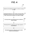
FIG. 4 is an example flowchart of a method 400 for refreshing a row address if a counter threshold is exceeded. Although execution of the method 400 is described below with reference to the device 100, other suitable components for execution of the method 400 can be utilized, such as the device 200. Additionally, the components for executing the method 400 may be spread among multiple devices (e.g., a processing device in communication with input and output devices). In certain scenarios, multiple devices acting in coordination can be considered a single device to perform the method 400. The method 400 may be implemented in the form of executable instructions stored on a machine-readable storage medium, such as storage medium 320, and/or in the form of electronic circuitry.
At block 410, the device 100 determines if an activated row address of a memory is included in a table 110. Then, at block 420, the device 100 increments a first counter 122-1 of a first row address 112-1 of the table 110 and/or a second counter 122-2 of a second row address 112-2 of the table 110, if the activated row address is not included in the table 110. Next, at block 430, the device 100 compares the first and/or second counters 122-1 and 122-2 to a counter threshold 152.
At block 440, the device 100 refreshes the first row address 112-1 if the first counter 122-1 exceeds the counter threshold 152. At block 450, the device 100 refreshes the second row address 112-2 if the second counter 122-2 exceeds the counter threshold 152. The first and second row addresses 112-1 and 112-2 are adjacent to the activated row address at the memory.
FIGS. 5A to 5D is another example flowchart of a method 500 for refreshing a row address if a counter threshold is exceeded. Although execution of the method 500 is described below with reference to the device 200, other suitable components for execution of the method 500 can be utilized, such as the device 100. Additionally, the components for executing the method 500 may be spread among multiple devices (e.g., a processing device in communication with input and output devices). In certain scenarios, multiple devices acting in coordination can be considered a single device to perform the method 500. The method 500 may be implemented in the form of executable instructions stored on a machine-readable storage medium, such as storage medium 320, and/or in the form of electronic circuitry.
Starting with FIG. 5A, the method 500 starts at point A and flows to block 502 where the device 200 determines if an activated row address of a memory 250 is included in a table 110. If the activated row address 112-3 is included in the table 110, the device 200 resets a third counter 122-3 at block 504 and then sets a third LRU field 212-3 to a minimum value at block 506. Next, the method 500 flows to point D, as explained further below. On the other hand, if the activated row address is not included in the table 110, the method 500 flows from block 502 to block 508.
At block 508, the device 200 determines if the first row address 112-1 is included in the table 110. If the first row address 112-1 is included in the table 110, the method 500 flows to block 510, where the device 200 increments a first counter 122-1. Then, at block 512, the device 200 determines if the first counter 122-1 exceeds the counter threshold 152. If the first counter 122-1 exceeds the counter threshold 152, the method 500 flows to point E, as explained in further detail below. On the other hand, if the first counter 122-1 does not exceed the counter threshold 152, the method 500 flows to block 514, where the device 200 sets a first LRU field 212-1 to a maximum value, and then flows to point D.
Returning back to block 508, the device 200 determines if the first row address 112-1 is not included in the table 110, the method 500 flows to point B, as explained in greater detail below. Regardless of whether the first row address 112-1 is included in the table 110, the method 600 further flows to block 516, where the device 200 determines if the second row address 112-2 is included in the table 110.
If the second row address 112-2 is included in the table 110, the method 500 flows to block 518, where the device 200 increments a second counter 122-2. Then, at block 520, the device 200 determines if the second counter 122-2 exceeds the counter threshold 152. If the second counter 122-2 exceeds the counter threshold 152, the method 500 flows to point F, as explained in further detail below. On the other hand, if the second counter 122-2 does not exceed the counter threshold 152, the method 500 flows to block 522, where the device 200 sets a second LRU field 212-2 to then maximum value, and then flows to point D.
FIG. 5B illustrates a continuation from points B and C. As shown in FIG. 5A, when the first row address 112-1 is not included in the table 110, the method 500 flows to Point B, which then flows to block 524 of FIG. 5B. At block 524, the device 200 determines if the table 110 is full. If the table 110 is full, the method 500 flows to block 526, where the device 200 selects one of the plurality of row addresses 112-1 to 112-n to remove from the table 110 based on a value of the plurality of counters 122-1 to 122-n and the plurality of LRU fields 212-1 to 212-n. Each of the counters 122-1 to 122-n corresponds to one of the row addresses 112-1 to 112-n and each of the LRU fields 212-1 to 212-n corresponds to one of the row addresses 112-1 to 112-n.
For example, the row address 112 having an LRU field 212 below the minimum value and a lowest value for its counter 122 may be selected to be removed. Next, the method 500 flows from block 526 to block 528. The method 500 similarly flows from block 524 to block 528, if the table 110 is not full. At block 528, the device 200 adds the first row address 112-1 to the table 110. Lastly, at block 530, the device 200 sets the first LRU 212-1 to the maximum value. The method 500 then flows to point D.
As shown in FIG. 5A, when the second row address 112-2 is not included in the table 110, the method 500 flows to Point C, which then flows to block 532 of FIG. 5B. At block 532, the device 200 determines if the table 110 is full. If the table 110 is full, the method 500 flows to block 534, where the device 200 selects one of the plurality of row addresses 112-1 to 112-n to remove from the table 110 based on the value of the plurality of counters 122-1 to 122-n and the plurality of LRU fields 212-1 to 212-n, as explained above.
Next, the method 500 flows from block 534 to block 536. The method 500 similarly flows from block 532 to block 536, if the table 110 is not full. At block 536, the device 200 adds the second row address 112-2 to the table 110. Lastly, at block 538, the device 200 sets the second LRU 212-2 to the maximum value. The method 500 then flows to point D.
FIG. 5C illustrates a continuation from points D, E and F. Point D flows to block 540, where the device 200 decrements all of the plurality of LRU fields 2121-1 to 212-n. As shown in FIG. 5A, when the first counter 122-1 exceeds the counter threshold 152, the method 500 flows to point E, when then flows to block 542 of FIG. 5C. At block 542, the device 200 refreshes the first row address 112-1. Then, at block 544, the device 200 resets the first counter 122-1. Next, the device 200 sets the first LRU 212-1 to the minimum value. After, the method 500 flows to point D.
As shown in FIG. 5A, when the second counter 122-2 exceeds the counter threshold 152, the method 500 flows to point F, when then flows to block 548 of FIG. 5C. At block 548, the device 200 refreshes the second row address 112-2. Then, at block 550, the device 200 resets the second counter 122-2. Next, the device 200 sets the second LRU 212-2 to the minimum value. After, the method 500 flows to point D.
FIG. 5D illustrates a process occurring simultaneously with the process shown in FIGS. 5A to 5C. At block 554, the device 200 determines if a refresh interval 240 has expired. If the refresh interval 240 has expired, the device 200 resets all of the plurality of counters 122-1 to 122-n and all of the plurality of LRU fields 212-1 to 212-n, at block 556. The method 500 then flows back to block 554, where the device 200 continues to wait for the next refresh interval 240 to expire.

Claims (15)

I claim:
1. A device, comprising:
a table to store a plurality of row addresses, including first and second row addresses, of a memory;
a plurality of counters including first and second counters, each of the counters to correspond to one of the row addresses of the table;
a row unit to determine if an activated row address of the memory is included in the table;
a counter unit to increment at least one of the first counter of the first row address and the second counter of the second row address, if the activated row address is not included in the table; and
a refresh unit to refresh at least one of the first and second row addresses if at least one of the first and second counters exceeds a counter threshold, wherein
at least one the first and second row addresses are adjacent to the activated row address.
2. The device of claim 1, wherein,
the refresh unit is to refresh the first row address and the counter unit is to reset the first counter to a minimum value, if the first counter exceeds the counter threshold, and
the refresh unit is to refresh the second row address and the counter unit is to reset the second counter to the minimum value, if the second counter exceeds the counter threshold.
3. The device of claim 1, wherein the counter unit is to reset a third counter of the activated row address to a minimum value if the activated row address is included in the table.
4. The device of claim 1, wherein the counter unit is to add at least one of the first and second row addresses to the table, if the table does not include at least one of the first and second row addresses and the activated row address is not included in the table.
5. The device of claim 4, further comprising,
a least recently used (LRU) unit to,
set at least one of a first LRU field of the first row address and second LRU field of the second row address to a maximum value, if the activated row address is not included in the table,
set at least one of the first and second LRU fields to a minimum value, if at one of the first and second row addresses is refreshed, and
set a third LRU field of the activated row address to the minimum value, if the activated row address is included in the table.
6. The device of claim 5, further comprising:
a replacement unit to select one of the plurality of row addresses to have a set replacement status if the selected row address is to have an LRU field less than the minimum value and to correspond to a counter having a lowest value of the plurality of counters, wherein,
the LRU unit is to decrement all of the LRU fields each time a row address of the memory is to be activated.
7. The device of claim 6, wherein the replacement unit is to replace the row address of the table having the set replacement status with at least one of the first and second row addresses, if the table is full and at least one of the first and second row addresses is not included in the table.
8. The device of claim 6, wherein,
all of the plurality of counters and LRU fields are to be reset at an end of a refresh interval,
the activated row address is activated in response to an activate command, and
at least one of the first and second rows are refreshed via a read command.
9. A method, comprising:
determining if an activated row address of a memory is included in a table;
incrementing at least one of a first counter of a first row address of the table and a second counter of a second row address of the table, if the activated row address is not included in the table;
comparing at least one of the first and second counters to a counter threshold;
refreshing the first row address if the first counter exceeds the counter threshold; and
refreshing the second row address if the second counter exceeds the counter threshold, wherein
the first and second row addresses are adjacent to the activated row address at the memory.
10. The method of claim 9, further comprising:
resetting a third counter of the activated row address, if the activated row address is in included in the table; and
resetting at least one of the first and second counters if at least one of the first and second row addresses is refreshed.
11. The method of claim 9, further comprising:
adding at least one of the first and second row addresses to the table, if at least one of the first and second row addresses are not included in the table, wherein
at least one of the row addresses of the table is removed, if the table is full and one of the first and row addresses is being added to the table, and
the at least one removed row address to be selected based on a value of the counter and a least recently used (LRU) value of the removed row address.
12. The method of claim 11, further comprising:
setting at least one of a first LRU field of the first row address and a second LRU field of the second row address to a minimum value, if at least one of the first and second row addresses is refreshed, and
setting a third LRU field of the activated row address to the minimum value, if the activated row address is included in the table.
13. The method of claim 12, further comprising:
decrementing all of the LRU fields each time a row address of the memory is activated;
resetting all of the counters and all of the LRU fields, if a refresh interval expires;
setting at least one of the first and second LRU fields to a maximum value after at least one of the first and second counters is incremented; and setting at least one of the first and second LRU fields to the maximum value if at least one of the first and second row addresses is added to the table.
14. A non-transitory computer-readable storage medium storing instructions that, if executed by a processor of a device, cause the processor to:
increment a first counter of a first row address of a table, if an activated row address adjacent to the first row address is not included in the table;
increment a second counter of a second row address of the table, if the activated row address adjacent to the second row address is not included in the table;
refresh the first row address if the first counter exceeds a counter threshold; and
refresh the second row address if the second counter exceeds the counter threshold.
15. The non-transitory computer-readable storage medium of claim 14, further comprising instructions that, if executed by a processor of a device, cause the processor to,
reset the first counter if the first row address is refreshed; and
reset the second counter if the second row address is refreshed, wherein
the activated row address is between the first and second row addresses.
US14/912,502 2013-09-27 2013-09-27 Refresh row address Active US9690505B2 (en)

Applications Claiming Priority (1)

Application Number Priority Date Filing Date Title
PCT/US2013/062233 WO2015047304A1 (en) 2013-09-27 2013-09-27 Refresh row address

Publications (2)

Publication Number Publication Date
US20160202926A1 US20160202926A1 (en) 2016-07-14
US9690505B2 true US9690505B2 (en) 2017-06-27

Family

ID=52744207

Family Applications (1)

Application Number Title Priority Date Filing Date
US14/912,502 Active US9690505B2 (en) 2013-09-27 2013-09-27 Refresh row address

Country Status (2)

Country Link
US (1) US9690505B2 (en)
WO (1) WO2015047304A1 (en)

Cited By (5)

* Cited by examiner, † Cited by third party
Publication number Priority date Publication date Assignee Title
WO2020139422A1 (en) * 2018-12-27 2020-07-02 Micron Technology, Inc. An apparatus with a row-hammer address latch mechanism
US10811077B2 (en) 2018-05-14 2020-10-20 Samsung Electronics Co., Ltd. Refresh control circuit, memory device including the same and method of operating the same for hammer refresh operation
US10902902B2 (en) * 2017-05-24 2021-01-26 SK Hynix Inc. Memory system and operation method of memory system
US20220208237A1 (en) * 2020-12-24 2022-06-30 Samsung Electronics Co., Ltd. Semiconductor device and electronic device including the same
US11532336B2 (en) 2020-09-16 2022-12-20 Samsung Electronics Co., Ltd. Memory device for processing a row-hammer refresh operation and a method of operating thereof

Families Citing this family (54)

* Cited by examiner, † Cited by third party
Publication number Priority date Publication date Assignee Title
US9324398B2 (en) 2013-02-04 2016-04-26 Micron Technology, Inc. Apparatuses and methods for targeted refreshing of memory
US9269436B2 (en) 2013-03-12 2016-02-23 Intel Corporation Techniques for determining victim row addresses in a volatile memory
US9449671B2 (en) * 2013-03-15 2016-09-20 Intel Corporation Techniques for probabilistic dynamic random access memory row repair
US9047978B2 (en) 2013-08-26 2015-06-02 Micron Technology, Inc. Apparatuses and methods for selective row refreshes
JP2015219938A (en) 2014-05-21 2015-12-07 マイクロン テクノロジー, インク. Semiconductor device
US9812185B2 (en) * 2015-10-21 2017-11-07 Invensas Corporation DRAM adjacent row disturb mitigation
KR102403341B1 (en) * 2016-03-17 2022-06-02 에스케이하이닉스 주식회사 Memory and system including the same
JP2017182854A (en) 2016-03-31 2017-10-05 マイクロン テクノロジー, インク. Semiconductor device
US10490251B2 (en) 2017-01-30 2019-11-26 Micron Technology, Inc. Apparatuses and methods for distributing row hammer refresh events across a memory device
US10198369B2 (en) * 2017-03-24 2019-02-05 Advanced Micro Devices, Inc. Dynamic memory remapping to reduce row-buffer conflicts
WO2019026197A1 (en) * 2017-08-02 2019-02-07 ゼンテルジャパン株式会社 Semiconductor storage device
KR20190033387A (en) * 2017-09-21 2019-03-29 에스케이하이닉스 주식회사 Memory system and operating method thereof
US10580475B2 (en) 2018-01-22 2020-03-03 Micron Technology, Inc. Apparatuses and methods for calculating row hammer refresh addresses in a semiconductor device
US11017833B2 (en) 2018-05-24 2021-05-25 Micron Technology, Inc. Apparatuses and methods for pure-time, self adopt sampling for row hammer refresh sampling
US11152050B2 (en) 2018-06-19 2021-10-19 Micron Technology, Inc. Apparatuses and methods for multiple row hammer refresh address sequences
US10573370B2 (en) 2018-07-02 2020-02-25 Micron Technology, Inc. Apparatus and methods for triggering row hammer address sampling
US10825534B2 (en) * 2018-10-26 2020-11-03 Intel Corporation Per row activation count values embedded in storage cell array storage cells
US10685696B2 (en) 2018-10-31 2020-06-16 Micron Technology, Inc. Apparatuses and methods for access based refresh timing
CN113168861B (en) 2018-12-03 2024-05-14 美光科技公司 Semiconductor device performing row hammer refresh operation
CN117198356A (en) 2018-12-21 2023-12-08 美光科技公司 Apparatus and method for timing interleaving for targeted refresh operations
US10957377B2 (en) 2018-12-26 2021-03-23 Micron Technology, Inc. Apparatuses and methods for distributed targeted refresh operations
US10770127B2 (en) 2019-02-06 2020-09-08 Micron Technology, Inc. Apparatuses and methods for managing row access counts
US11615831B2 (en) 2019-02-26 2023-03-28 Micron Technology, Inc. Apparatuses and methods for memory mat refresh sequencing
US11043254B2 (en) 2019-03-19 2021-06-22 Micron Technology, Inc. Semiconductor device having cam that stores address signals
US11227649B2 (en) 2019-04-04 2022-01-18 Micron Technology, Inc. Apparatuses and methods for staggered timing of targeted refresh operations
US11264096B2 (en) 2019-05-14 2022-03-01 Micron Technology, Inc. Apparatuses, systems, and methods for a content addressable memory cell with latch and comparator circuits
US11158364B2 (en) * 2019-05-31 2021-10-26 Micron Technology, Inc. Apparatuses and methods for tracking victim rows
US11069393B2 (en) 2019-06-04 2021-07-20 Micron Technology, Inc. Apparatuses and methods for controlling steal rates
US10978132B2 (en) 2019-06-05 2021-04-13 Micron Technology, Inc. Apparatuses and methods for staggered timing of skipped refresh operations
US11158373B2 (en) 2019-06-11 2021-10-26 Micron Technology, Inc. Apparatuses, systems, and methods for determining extremum numerical values
US11139015B2 (en) 2019-07-01 2021-10-05 Micron Technology, Inc. Apparatuses and methods for monitoring word line accesses
US10832792B1 (en) 2019-07-01 2020-11-10 Micron Technology, Inc. Apparatuses and methods for adjusting victim data
US11386946B2 (en) 2019-07-16 2022-07-12 Micron Technology, Inc. Apparatuses and methods for tracking row accesses
US10943636B1 (en) 2019-08-20 2021-03-09 Micron Technology, Inc. Apparatuses and methods for analog row access tracking
US10964378B2 (en) * 2019-08-22 2021-03-30 Micron Technology, Inc. Apparatus and method including analog accumulator for determining row access rate and target row address used for refresh operation
US11302374B2 (en) 2019-08-23 2022-04-12 Micron Technology, Inc. Apparatuses and methods for dynamic refresh allocation
US11200942B2 (en) 2019-08-23 2021-12-14 Micron Technology, Inc. Apparatuses and methods for lossy row access counting
US11302377B2 (en) 2019-10-16 2022-04-12 Micron Technology, Inc. Apparatuses and methods for dynamic targeted refresh steals
US11361811B2 (en) 2020-06-23 2022-06-14 Upmem Method and circuit for protecting a DRAM memory device from the row hammer effect
FR3111731B1 (en) * 2020-06-23 2023-01-06 Upmem Method and circuit for protecting a DRAM memory device from the rank hammering effect
US11309010B2 (en) 2020-08-14 2022-04-19 Micron Technology, Inc. Apparatuses, systems, and methods for memory directed access pause
US11348631B2 (en) 2020-08-19 2022-05-31 Micron Technology, Inc. Apparatuses, systems, and methods for identifying victim rows in a memory device which cannot be simultaneously refreshed
US11380382B2 (en) 2020-08-19 2022-07-05 Micron Technology, Inc. Refresh logic circuit layout having aggressor detector circuit sampling circuit and row hammer refresh control circuit
US11222682B1 (en) 2020-08-31 2022-01-11 Micron Technology, Inc. Apparatuses and methods for providing refresh addresses
US11557331B2 (en) 2020-09-23 2023-01-17 Micron Technology, Inc. Apparatuses and methods for controlling refresh operations
US11222686B1 (en) 2020-11-12 2022-01-11 Micron Technology, Inc. Apparatuses and methods for controlling refresh timing
US11462291B2 (en) 2020-11-23 2022-10-04 Micron Technology, Inc. Apparatuses and methods for tracking word line accesses
US11264079B1 (en) 2020-12-18 2022-03-01 Micron Technology, Inc. Apparatuses and methods for row hammer based cache lockdown
US11482275B2 (en) 2021-01-20 2022-10-25 Micron Technology, Inc. Apparatuses and methods for dynamically allocated aggressor detection
US11600314B2 (en) 2021-03-15 2023-03-07 Micron Technology, Inc. Apparatuses and methods for sketch circuits for refresh binning
US11664063B2 (en) 2021-08-12 2023-05-30 Micron Technology, Inc. Apparatuses and methods for countering memory attacks
KR20230072283A (en) * 2021-11-17 2023-05-24 삼성전자주식회사 Memory device, memory system having the same and operating method thereof
US11688451B2 (en) 2021-11-29 2023-06-27 Micron Technology, Inc. Apparatuses, systems, and methods for main sketch and slim sketch circuit for row address tracking
US11948656B1 (en) * 2022-09-21 2024-04-02 Micron Technology, Inc. Counter management for memory systems

Citations (14)

* Cited by examiner, † Cited by third party
Publication number Priority date Publication date Assignee Title
US5410545A (en) 1992-07-28 1995-04-25 Digital Equipment Corporation Long-term storage of controller performance
US6061290A (en) 1997-06-30 2000-05-09 Micron Technology, Inc. Method and apparatus for simultaneous memory subarray testing
US20070030746A1 (en) 2005-08-04 2007-02-08 Best Scott C Memory device testing to support address-differentiated refresh rates
US20090268539A1 (en) 2008-04-23 2009-10-29 Hermann Ruckerbauer Chip, Multi-Chip System in a Method for Performing a Refresh of a Memory Array
US20110069572A1 (en) 2009-09-18 2011-03-24 Samsung Electronics Co., Ltd. Row address code selection based on locations of substandard memory cells
US8164941B2 (en) 2006-12-27 2012-04-24 Hynix Semiconductor Inc. Semiconductor memory device with ferroelectric device and refresh method thereof
US20120151131A1 (en) 2010-12-09 2012-06-14 International Business Machines Corporation Memory system with a programmable refresh cycle
US20130003467A1 (en) 2004-07-15 2013-01-03 Micron Technology, Inc. Digit line comparison circuits
US20130268727A1 (en) * 2012-04-10 2013-10-10 Kyo Min Sohn Memory system for access concentration decrease management and access concentration decrease method
US20130326162A1 (en) * 2012-06-04 2013-12-05 SK Hynix Inc. Semiconductor device and operating method thereof
US20140095780A1 (en) * 2012-09-28 2014-04-03 Kuljit S. Bains Distributed row hammer tracking
US20140177370A1 (en) * 2012-12-21 2014-06-26 Intel Corporation Method, apparatus and system for responding to a row hammer event
US20140189228A1 (en) * 2012-12-28 2014-07-03 Zaika Greenfield Throttling support for row-hammer counters
US20160246525A1 (en) * 2013-08-20 2016-08-25 Oracle International Corporation Detection of multiple accesses to a row address of a dynamic memory within a refresh period

Patent Citations (14)

* Cited by examiner, † Cited by third party
Publication number Priority date Publication date Assignee Title
US5410545A (en) 1992-07-28 1995-04-25 Digital Equipment Corporation Long-term storage of controller performance
US6061290A (en) 1997-06-30 2000-05-09 Micron Technology, Inc. Method and apparatus for simultaneous memory subarray testing
US20130003467A1 (en) 2004-07-15 2013-01-03 Micron Technology, Inc. Digit line comparison circuits
US20070030746A1 (en) 2005-08-04 2007-02-08 Best Scott C Memory device testing to support address-differentiated refresh rates
US8164941B2 (en) 2006-12-27 2012-04-24 Hynix Semiconductor Inc. Semiconductor memory device with ferroelectric device and refresh method thereof
US20090268539A1 (en) 2008-04-23 2009-10-29 Hermann Ruckerbauer Chip, Multi-Chip System in a Method for Performing a Refresh of a Memory Array
US20110069572A1 (en) 2009-09-18 2011-03-24 Samsung Electronics Co., Ltd. Row address code selection based on locations of substandard memory cells
US20120151131A1 (en) 2010-12-09 2012-06-14 International Business Machines Corporation Memory system with a programmable refresh cycle
US20130268727A1 (en) * 2012-04-10 2013-10-10 Kyo Min Sohn Memory system for access concentration decrease management and access concentration decrease method
US20130326162A1 (en) * 2012-06-04 2013-12-05 SK Hynix Inc. Semiconductor device and operating method thereof
US20140095780A1 (en) * 2012-09-28 2014-04-03 Kuljit S. Bains Distributed row hammer tracking
US20140177370A1 (en) * 2012-12-21 2014-06-26 Intel Corporation Method, apparatus and system for responding to a row hammer event
US20140189228A1 (en) * 2012-12-28 2014-07-03 Zaika Greenfield Throttling support for row-hammer counters
US20160246525A1 (en) * 2013-08-20 2016-08-25 Oracle International Corporation Detection of multiple accesses to a row address of a dynamic memory within a refresh period

Non-Patent Citations (3)

* Cited by examiner, † Cited by third party
Title
Fischer, et al, "FPGA Design for DDR3 Memory," < http://www.wpi.edu/Pubs/E-project/Available/E-project-031212-183607/unrestricted/FPGA-Design-for-DDR3-Memory.pdf >, Mar. 12, 2012 (135 pages).
Fischer, et al, "FPGA Design for DDR3 Memory," < http://www.wpi.edu/Pubs/E-project/Available/E-project-031212-183607/unrestricted/FPGA—Design—for—DDR3—Memory.pdf >, Mar. 12, 2012 (135 pages).
International Searching Authority, The International Search Report and the Written Opinion for PCT/US2013/062233 dated Jun. 10, 2014, 9 Pages.

Cited By (8)

* Cited by examiner, † Cited by third party
Publication number Priority date Publication date Assignee Title
US10902902B2 (en) * 2017-05-24 2021-01-26 SK Hynix Inc. Memory system and operation method of memory system
US10811077B2 (en) 2018-05-14 2020-10-20 Samsung Electronics Co., Ltd. Refresh control circuit, memory device including the same and method of operating the same for hammer refresh operation
WO2020139422A1 (en) * 2018-12-27 2020-07-02 Micron Technology, Inc. An apparatus with a row-hammer address latch mechanism
US10943637B2 (en) 2018-12-27 2021-03-09 Micron Technology, Inc. Apparatus with a row-hammer address latch mechanism
US11610623B2 (en) 2018-12-27 2023-03-21 Micron Technology, Inc. Apparatus with a row-hammer address latch mechanism
US11532336B2 (en) 2020-09-16 2022-12-20 Samsung Electronics Co., Ltd. Memory device for processing a row-hammer refresh operation and a method of operating thereof
US20220208237A1 (en) * 2020-12-24 2022-06-30 Samsung Electronics Co., Ltd. Semiconductor device and electronic device including the same
US11915782B2 (en) * 2020-12-24 2024-02-27 Samsung Electronics Co., Ltd. Semiconductor device and electronic device including the same

Also Published As

Publication number Publication date
US20160202926A1 (en) 2016-07-14
WO2015047304A1 (en) 2015-04-02

Similar Documents

Publication Publication Date Title
US9690505B2 (en) Refresh row address
CN107068175B (en) Volatile memory device, information providing method thereof, and refresh control method thereof
US11222682B1 (en) Apparatuses and methods for providing refresh addresses
US10108357B2 (en) Detection of multiple accesses to a row address of a dynamic memory within a refresh period
US9293188B2 (en) Memory and memory controller for high reliability operation and method
US9165637B2 (en) Volatile memory device and a memory controller
US9685218B2 (en) Memory device and memory system having the same
US9281046B2 (en) Data processor with memory controller for high reliability operation and method
US9767882B2 (en) Method of refreshing memory device
EP3462320B1 (en) Dynamic page allocation in memory
CN105808455B (en) Memory access method, storage-class memory and computer system
US10468092B2 (en) Memory device for controlling refresh operation by using cell characteristic flags
US11195568B1 (en) Methods and systems for controlling refresh operations of a memory device
US10824365B2 (en) Magnetoresistive memory module and computing device including the same
KR20160116533A (en) Memory controller and memory system managing refresh operation and operating method thereof
US11216386B2 (en) Techniques for setting a 2-level auto-close timer to access a memory device
US9824743B2 (en) Memory refresh operation with page open
US9972379B2 (en) First data in response to second read request
US20230410875A1 (en) Memory device and defense method thereof
US20220246200A1 (en) Memory device skipping refresh operation and operation method thereof
US8639879B2 (en) Sorting movable memory hierarchies in a computer system
KR20140081162A (en) Memory controller and memory system including the same
US10185510B2 (en) Bank interleaving controller and semiconductor device including the same
US20240112717A1 (en) Memory with deterministic worst-case row address servicing, and associated systems, devices, and methods
TWI660270B (en) Dynamic random access memory and method for operating the same

Legal Events

Date Code Title Description
AS Assignment

Owner name: HEWLETT-PACKARD DEVELOPMENT COMPANY, L.P., TEXAS

Free format text: ASSIGNMENT OF ASSIGNORS INTEREST;ASSIGNOR:BENEDICT, MELVIN K.;REEL/FRAME:037755/0533

Effective date: 20130925

AS Assignment

Owner name: HEWLETT PACKARD ENTERPRISE DEVELOPMENT LP, TEXAS

Free format text: ASSIGNMENT OF ASSIGNORS INTEREST;ASSIGNOR:HEWLETT-PACKARD DEVELOPMENT COMPANY, L.P.;REEL/FRAME:037907/0070

Effective date: 20151027

STCF Information on status: patent grant

Free format text: PATENTED CASE

MAFP Maintenance fee payment

Free format text: PAYMENT OF MAINTENANCE FEE, 4TH YEAR, LARGE ENTITY (ORIGINAL EVENT CODE: M1551); ENTITY STATUS OF PATENT OWNER: LARGE ENTITY

Year of fee payment: 4