US9659885B2 - Semiconductor device with pre-molding chip bonding - Google Patents
Semiconductor device with pre-molding chip bonding Download PDFInfo
- Publication number
- US9659885B2 US9659885B2 US14/493,718 US201414493718A US9659885B2 US 9659885 B2 US9659885 B2 US 9659885B2 US 201414493718 A US201414493718 A US 201414493718A US 9659885 B2 US9659885 B2 US 9659885B2
- Authority
- US
- United States
- Prior art keywords
- layer
- bonding layer
- semiconductor device
- adhesive
- chip
- Prior art date
- Legal status (The legal status is an assumption and is not a legal conclusion. Google has not performed a legal analysis and makes no representation as to the accuracy of the status listed.)
- Active
Links
- 239000004065 semiconductor Substances 0.000 title claims abstract description 52
- 238000000465 moulding Methods 0.000 title abstract description 22
- 238000009826 distribution Methods 0.000 claims abstract description 27
- 239000010410 layer Substances 0.000 claims description 157
- 239000012790 adhesive layer Substances 0.000 claims description 39
- 239000000853 adhesive Substances 0.000 claims description 21
- 230000001070 adhesive effect Effects 0.000 claims description 21
- 239000004593 Epoxy Substances 0.000 claims description 9
- 239000000463 material Substances 0.000 claims description 9
- 229910000679 solder Inorganic materials 0.000 claims description 8
- 239000004952 Polyamide Substances 0.000 claims description 4
- 229920002647 polyamide Polymers 0.000 claims description 4
- 230000009257 reactivity Effects 0.000 claims description 3
- 238000000926 separation method Methods 0.000 claims 2
- 238000003825 pressing Methods 0.000 abstract description 6
- 238000004519 manufacturing process Methods 0.000 abstract description 4
- 238000000034 method Methods 0.000 description 28
- 230000008878 coupling Effects 0.000 description 8
- 238000010168 coupling process Methods 0.000 description 8
- 238000005859 coupling reaction Methods 0.000 description 8
- 150000001875 compounds Chemical class 0.000 description 6
- VYPSYNLAJGMNEJ-UHFFFAOYSA-N Silicium dioxide Chemical compound O=[Si]=O VYPSYNLAJGMNEJ-UHFFFAOYSA-N 0.000 description 4
- 238000007906 compression Methods 0.000 description 3
- 230000006835 compression Effects 0.000 description 3
- 239000000945 filler Substances 0.000 description 3
- 239000000203 mixture Substances 0.000 description 3
- 229910052710 silicon Inorganic materials 0.000 description 3
- 239000010703 silicon Substances 0.000 description 3
- 229910052681 coesite Inorganic materials 0.000 description 2
- 229910052906 cristobalite Inorganic materials 0.000 description 2
- 238000010586 diagram Methods 0.000 description 2
- 230000006870 function Effects 0.000 description 2
- 238000003780 insertion Methods 0.000 description 2
- 230000037431 insertion Effects 0.000 description 2
- 238000005498 polishing Methods 0.000 description 2
- 239000000377 silicon dioxide Substances 0.000 description 2
- 229910052682 stishovite Inorganic materials 0.000 description 2
- 229910052905 tridymite Inorganic materials 0.000 description 2
- 229920000106 Liquid crystal polymer Polymers 0.000 description 1
- 239000004977 Liquid-crystal polymers (LCPs) Substances 0.000 description 1
- 239000004642 Polyimide Substances 0.000 description 1
- 229920001486 SU-8 photoresist Polymers 0.000 description 1
- 230000003466 anti-cipated effect Effects 0.000 description 1
- 230000015556 catabolic process Effects 0.000 description 1
- 239000000919 ceramic Substances 0.000 description 1
- 238000004132 cross linking Methods 0.000 description 1
- 239000003989 dielectric material Substances 0.000 description 1
- 238000009472 formulation Methods 0.000 description 1
- 239000011521 glass Substances 0.000 description 1
- 238000010438 heat treatment Methods 0.000 description 1
- 239000011256 inorganic filler Substances 0.000 description 1
- 229910003475 inorganic filler Inorganic materials 0.000 description 1
- 239000011368 organic material Substances 0.000 description 1
- 230000035515 penetration Effects 0.000 description 1
- 229920001721 polyimide Polymers 0.000 description 1
- 239000011347 resin Substances 0.000 description 1
- 229920005989 resin Polymers 0.000 description 1
- 229910001220 stainless steel Inorganic materials 0.000 description 1
- 239000010935 stainless steel Substances 0.000 description 1
Images


Classifications
-
- H—ELECTRICITY
- H01—ELECTRIC ELEMENTS
- H01L—SEMICONDUCTOR DEVICES NOT COVERED BY CLASS H10
- H01L24/00—Arrangements for connecting or disconnecting semiconductor or solid-state bodies; Methods or apparatus related thereto
- H01L24/01—Means for bonding being attached to, or being formed on, the surface to be connected, e.g. chip-to-package, die-attach, "first-level" interconnects; Manufacturing methods related thereto
- H01L24/02—Bonding areas ; Manufacturing methods related thereto
- H01L24/04—Structure, shape, material or disposition of the bonding areas prior to the connecting process
- H01L24/05—Structure, shape, material or disposition of the bonding areas prior to the connecting process of an individual bonding area
-
- H—ELECTRICITY
- H01—ELECTRIC ELEMENTS
- H01L—SEMICONDUCTOR DEVICES NOT COVERED BY CLASS H10
- H01L21/00—Processes or apparatus adapted for the manufacture or treatment of semiconductor or solid state devices or of parts thereof
- H01L21/02—Manufacture or treatment of semiconductor devices or of parts thereof
- H01L21/04—Manufacture or treatment of semiconductor devices or of parts thereof the devices having potential barriers, e.g. a PN junction, depletion layer or carrier concentration layer
- H01L21/50—Assembly of semiconductor devices using processes or apparatus not provided for in a single one of the subgroups H01L21/06 - H01L21/326, e.g. sealing of a cap to a base of a container
- H01L21/56—Encapsulations, e.g. encapsulation layers, coatings
- H01L21/561—Batch processing
-
- H—ELECTRICITY
- H01—ELECTRIC ELEMENTS
- H01L—SEMICONDUCTOR DEVICES NOT COVERED BY CLASS H10
- H01L21/00—Processes or apparatus adapted for the manufacture or treatment of semiconductor or solid state devices or of parts thereof
- H01L21/02—Manufacture or treatment of semiconductor devices or of parts thereof
- H01L21/04—Manufacture or treatment of semiconductor devices or of parts thereof the devices having potential barriers, e.g. a PN junction, depletion layer or carrier concentration layer
- H01L21/50—Assembly of semiconductor devices using processes or apparatus not provided for in a single one of the subgroups H01L21/06 - H01L21/326, e.g. sealing of a cap to a base of a container
- H01L21/56—Encapsulations, e.g. encapsulation layers, coatings
- H01L21/568—Temporary substrate used as encapsulation process aid
-
- H—ELECTRICITY
- H01—ELECTRIC ELEMENTS
- H01L—SEMICONDUCTOR DEVICES NOT COVERED BY CLASS H10
- H01L24/00—Arrangements for connecting or disconnecting semiconductor or solid-state bodies; Methods or apparatus related thereto
- H01L24/80—Methods for connecting semiconductor or other solid state bodies using means for bonding being attached to, or being formed on, the surface to be connected
- H01L24/82—Methods for connecting semiconductor or other solid state bodies using means for bonding being attached to, or being formed on, the surface to be connected by forming build-up interconnects at chip-level, e.g. for high density interconnects [HDI]
-
- H—ELECTRICITY
- H01—ELECTRIC ELEMENTS
- H01L—SEMICONDUCTOR DEVICES NOT COVERED BY CLASS H10
- H01L2221/00—Processes or apparatus adapted for the manufacture or treatment of semiconductor or solid state devices or of parts thereof covered by H01L21/00
- H01L2221/67—Apparatus for handling semiconductor or electric solid state devices during manufacture or treatment thereof; Apparatus for handling wafers during manufacture or treatment of semiconductor or electric solid state devices or components; Apparatus not specifically provided for elsewhere
- H01L2221/683—Apparatus for handling semiconductor or electric solid state devices during manufacture or treatment thereof; Apparatus for handling wafers during manufacture or treatment of semiconductor or electric solid state devices or components; Apparatus not specifically provided for elsewhere for supporting or gripping
- H01L2221/68304—Apparatus for handling semiconductor or electric solid state devices during manufacture or treatment thereof; Apparatus for handling wafers during manufacture or treatment of semiconductor or electric solid state devices or components; Apparatus not specifically provided for elsewhere for supporting or gripping using temporarily an auxiliary support
- H01L2221/68381—Details of chemical or physical process used for separating the auxiliary support from a device or wafer
-
- H—ELECTRICITY
- H01—ELECTRIC ELEMENTS
- H01L—SEMICONDUCTOR DEVICES NOT COVERED BY CLASS H10
- H01L2224/00—Indexing scheme for arrangements for connecting or disconnecting semiconductor or solid-state bodies and methods related thereto as covered by H01L24/00
- H01L2224/01—Means for bonding being attached to, or being formed on, the surface to be connected, e.g. chip-to-package, die-attach, "first-level" interconnects; Manufacturing methods related thereto
- H01L2224/02—Bonding areas; Manufacturing methods related thereto
- H01L2224/023—Redistribution layers [RDL] for bonding areas
- H01L2224/0237—Disposition of the redistribution layers
- H01L2224/02381—Side view
-
- H—ELECTRICITY
- H01—ELECTRIC ELEMENTS
- H01L—SEMICONDUCTOR DEVICES NOT COVERED BY CLASS H10
- H01L2224/00—Indexing scheme for arrangements for connecting or disconnecting semiconductor or solid-state bodies and methods related thereto as covered by H01L24/00
- H01L2224/01—Means for bonding being attached to, or being formed on, the surface to be connected, e.g. chip-to-package, die-attach, "first-level" interconnects; Manufacturing methods related thereto
- H01L2224/02—Bonding areas; Manufacturing methods related thereto
- H01L2224/04—Structure, shape, material or disposition of the bonding areas prior to the connecting process
- H01L2224/0401—Bonding areas specifically adapted for bump connectors, e.g. under bump metallisation [UBM]
-
- H—ELECTRICITY
- H01—ELECTRIC ELEMENTS
- H01L—SEMICONDUCTOR DEVICES NOT COVERED BY CLASS H10
- H01L2224/00—Indexing scheme for arrangements for connecting or disconnecting semiconductor or solid-state bodies and methods related thereto as covered by H01L24/00
- H01L2224/01—Means for bonding being attached to, or being formed on, the surface to be connected, e.g. chip-to-package, die-attach, "first-level" interconnects; Manufacturing methods related thereto
- H01L2224/02—Bonding areas; Manufacturing methods related thereto
- H01L2224/04—Structure, shape, material or disposition of the bonding areas prior to the connecting process
- H01L2224/04105—Bonding areas formed on an encapsulation of the semiconductor or solid-state body, e.g. bonding areas on chip-scale packages
-
- H—ELECTRICITY
- H01—ELECTRIC ELEMENTS
- H01L—SEMICONDUCTOR DEVICES NOT COVERED BY CLASS H10
- H01L2224/00—Indexing scheme for arrangements for connecting or disconnecting semiconductor or solid-state bodies and methods related thereto as covered by H01L24/00
- H01L2224/01—Means for bonding being attached to, or being formed on, the surface to be connected, e.g. chip-to-package, die-attach, "first-level" interconnects; Manufacturing methods related thereto
- H01L2224/10—Bump connectors; Manufacturing methods related thereto
- H01L2224/11—Manufacturing methods
-
- H—ELECTRICITY
- H01—ELECTRIC ELEMENTS
- H01L—SEMICONDUCTOR DEVICES NOT COVERED BY CLASS H10
- H01L2224/00—Indexing scheme for arrangements for connecting or disconnecting semiconductor or solid-state bodies and methods related thereto as covered by H01L24/00
- H01L2224/01—Means for bonding being attached to, or being formed on, the surface to be connected, e.g. chip-to-package, die-attach, "first-level" interconnects; Manufacturing methods related thereto
- H01L2224/10—Bump connectors; Manufacturing methods related thereto
- H01L2224/12—Structure, shape, material or disposition of the bump connectors prior to the connecting process
- H01L2224/12105—Bump connectors formed on an encapsulation of the semiconductor or solid-state body, e.g. bumps on chip-scale packages
-
- H—ELECTRICITY
- H01—ELECTRIC ELEMENTS
- H01L—SEMICONDUCTOR DEVICES NOT COVERED BY CLASS H10
- H01L2224/00—Indexing scheme for arrangements for connecting or disconnecting semiconductor or solid-state bodies and methods related thereto as covered by H01L24/00
- H01L2224/01—Means for bonding being attached to, or being formed on, the surface to be connected, e.g. chip-to-package, die-attach, "first-level" interconnects; Manufacturing methods related thereto
- H01L2224/10—Bump connectors; Manufacturing methods related thereto
- H01L2224/12—Structure, shape, material or disposition of the bump connectors prior to the connecting process
- H01L2224/13—Structure, shape, material or disposition of the bump connectors prior to the connecting process of an individual bump connector
- H01L2224/13001—Core members of the bump connector
- H01L2224/13099—Material
- H01L2224/131—Material with a principal constituent of the material being a metal or a metalloid, e.g. boron [B], silicon [Si], germanium [Ge], arsenic [As], antimony [Sb], tellurium [Te] and polonium [Po], and alloys thereof
-
- H—ELECTRICITY
- H01—ELECTRIC ELEMENTS
- H01L—SEMICONDUCTOR DEVICES NOT COVERED BY CLASS H10
- H01L2224/00—Indexing scheme for arrangements for connecting or disconnecting semiconductor or solid-state bodies and methods related thereto as covered by H01L24/00
- H01L2224/01—Means for bonding being attached to, or being formed on, the surface to be connected, e.g. chip-to-package, die-attach, "first-level" interconnects; Manufacturing methods related thereto
- H01L2224/18—High density interconnect [HDI] connectors; Manufacturing methods related thereto
- H01L2224/23—Structure, shape, material or disposition of the high density interconnect connectors after the connecting process
- H01L2224/24—Structure, shape, material or disposition of the high density interconnect connectors after the connecting process of an individual high density interconnect connector
- H01L2224/241—Disposition
- H01L2224/24135—Connecting between different semiconductor or solid-state bodies, i.e. chip-to-chip
- H01L2224/24137—Connecting between different semiconductor or solid-state bodies, i.e. chip-to-chip the bodies being arranged next to each other, e.g. on a common substrate
-
- H—ELECTRICITY
- H01—ELECTRIC ELEMENTS
- H01L—SEMICONDUCTOR DEVICES NOT COVERED BY CLASS H10
- H01L2224/00—Indexing scheme for arrangements for connecting or disconnecting semiconductor or solid-state bodies and methods related thereto as covered by H01L24/00
- H01L2224/80—Methods for connecting semiconductor or other solid state bodies using means for bonding being attached to, or being formed on, the surface to be connected
- H01L2224/82—Methods for connecting semiconductor or other solid state bodies using means for bonding being attached to, or being formed on, the surface to be connected by forming build-up interconnects at chip-level, e.g. for high density interconnects [HDI]
- H01L2224/82001—Methods for connecting semiconductor or other solid state bodies using means for bonding being attached to, or being formed on, the surface to be connected by forming build-up interconnects at chip-level, e.g. for high density interconnects [HDI] involving a temporary auxiliary member not forming part of the bonding apparatus
- H01L2224/82002—Methods for connecting semiconductor or other solid state bodies using means for bonding being attached to, or being formed on, the surface to be connected by forming build-up interconnects at chip-level, e.g. for high density interconnects [HDI] involving a temporary auxiliary member not forming part of the bonding apparatus being a removable or sacrificial coating
-
- H—ELECTRICITY
- H01—ELECTRIC ELEMENTS
- H01L—SEMICONDUCTOR DEVICES NOT COVERED BY CLASS H10
- H01L2224/00—Indexing scheme for arrangements for connecting or disconnecting semiconductor or solid-state bodies and methods related thereto as covered by H01L24/00
- H01L2224/80—Methods for connecting semiconductor or other solid state bodies using means for bonding being attached to, or being formed on, the surface to be connected
- H01L2224/82—Methods for connecting semiconductor or other solid state bodies using means for bonding being attached to, or being formed on, the surface to be connected by forming build-up interconnects at chip-level, e.g. for high density interconnects [HDI]
- H01L2224/82009—Pre-treatment of the connector or the bonding area
- H01L2224/8203—Reshaping, e.g. forming vias
-
- H—ELECTRICITY
- H01—ELECTRIC ELEMENTS
- H01L—SEMICONDUCTOR DEVICES NOT COVERED BY CLASS H10
- H01L2224/00—Indexing scheme for arrangements for connecting or disconnecting semiconductor or solid-state bodies and methods related thereto as covered by H01L24/00
- H01L2224/80—Methods for connecting semiconductor or other solid state bodies using means for bonding being attached to, or being formed on, the surface to be connected
- H01L2224/82—Methods for connecting semiconductor or other solid state bodies using means for bonding being attached to, or being formed on, the surface to be connected by forming build-up interconnects at chip-level, e.g. for high density interconnects [HDI]
- H01L2224/821—Forming a build-up interconnect
-
- H—ELECTRICITY
- H01—ELECTRIC ELEMENTS
- H01L—SEMICONDUCTOR DEVICES NOT COVERED BY CLASS H10
- H01L2224/00—Indexing scheme for arrangements for connecting or disconnecting semiconductor or solid-state bodies and methods related thereto as covered by H01L24/00
- H01L2224/93—Batch processes
- H01L2224/95—Batch processes at chip-level, i.e. with connecting carried out on a plurality of singulated devices, i.e. on diced chips
- H01L2224/96—Batch processes at chip-level, i.e. with connecting carried out on a plurality of singulated devices, i.e. on diced chips the devices being encapsulated in a common layer, e.g. neo-wafer or pseudo-wafer, said common layer being separable into individual assemblies after connecting
-
- H—ELECTRICITY
- H01—ELECTRIC ELEMENTS
- H01L—SEMICONDUCTOR DEVICES NOT COVERED BY CLASS H10
- H01L24/00—Arrangements for connecting or disconnecting semiconductor or solid-state bodies; Methods or apparatus related thereto
- H01L24/01—Means for bonding being attached to, or being formed on, the surface to be connected, e.g. chip-to-package, die-attach, "first-level" interconnects; Manufacturing methods related thereto
- H01L24/10—Bump connectors ; Manufacturing methods related thereto
- H01L24/11—Manufacturing methods
-
- H—ELECTRICITY
- H01—ELECTRIC ELEMENTS
- H01L—SEMICONDUCTOR DEVICES NOT COVERED BY CLASS H10
- H01L24/00—Arrangements for connecting or disconnecting semiconductor or solid-state bodies; Methods or apparatus related thereto
- H01L24/01—Means for bonding being attached to, or being formed on, the surface to be connected, e.g. chip-to-package, die-attach, "first-level" interconnects; Manufacturing methods related thereto
- H01L24/10—Bump connectors ; Manufacturing methods related thereto
- H01L24/12—Structure, shape, material or disposition of the bump connectors prior to the connecting process
- H01L24/13—Structure, shape, material or disposition of the bump connectors prior to the connecting process of an individual bump connector
-
- H—ELECTRICITY
- H01—ELECTRIC ELEMENTS
- H01L—SEMICONDUCTOR DEVICES NOT COVERED BY CLASS H10
- H01L24/00—Arrangements for connecting or disconnecting semiconductor or solid-state bodies; Methods or apparatus related thereto
- H01L24/01—Means for bonding being attached to, or being formed on, the surface to be connected, e.g. chip-to-package, die-attach, "first-level" interconnects; Manufacturing methods related thereto
- H01L24/18—High density interconnect [HDI] connectors; Manufacturing methods related thereto
- H01L24/19—Manufacturing methods of high density interconnect preforms
-
- H—ELECTRICITY
- H01—ELECTRIC ELEMENTS
- H01L—SEMICONDUCTOR DEVICES NOT COVERED BY CLASS H10
- H01L24/00—Arrangements for connecting or disconnecting semiconductor or solid-state bodies; Methods or apparatus related thereto
- H01L24/01—Means for bonding being attached to, or being formed on, the surface to be connected, e.g. chip-to-package, die-attach, "first-level" interconnects; Manufacturing methods related thereto
- H01L24/18—High density interconnect [HDI] connectors; Manufacturing methods related thereto
- H01L24/20—Structure, shape, material or disposition of high density interconnect preforms
-
- H—ELECTRICITY
- H01—ELECTRIC ELEMENTS
- H01L—SEMICONDUCTOR DEVICES NOT COVERED BY CLASS H10
- H01L24/00—Arrangements for connecting or disconnecting semiconductor or solid-state bodies; Methods or apparatus related thereto
- H01L24/01—Means for bonding being attached to, or being formed on, the surface to be connected, e.g. chip-to-package, die-attach, "first-level" interconnects; Manufacturing methods related thereto
- H01L24/18—High density interconnect [HDI] connectors; Manufacturing methods related thereto
- H01L24/23—Structure, shape, material or disposition of the high density interconnect connectors after the connecting process
- H01L24/24—Structure, shape, material or disposition of the high density interconnect connectors after the connecting process of an individual high density interconnect connector
-
- H—ELECTRICITY
- H01—ELECTRIC ELEMENTS
- H01L—SEMICONDUCTOR DEVICES NOT COVERED BY CLASS H10
- H01L2924/00—Indexing scheme for arrangements or methods for connecting or disconnecting semiconductor or solid-state bodies as covered by H01L24/00
-
- H—ELECTRICITY
- H01—ELECTRIC ELEMENTS
- H01L—SEMICONDUCTOR DEVICES NOT COVERED BY CLASS H10
- H01L2924/00—Indexing scheme for arrangements or methods for connecting or disconnecting semiconductor or solid-state bodies as covered by H01L24/00
- H01L2924/0001—Technical content checked by a classifier
- H01L2924/00012—Relevant to the scope of the group, the symbol of which is combined with the symbol of this group
-
- H—ELECTRICITY
- H01—ELECTRIC ELEMENTS
- H01L—SEMICONDUCTOR DEVICES NOT COVERED BY CLASS H10
- H01L2924/00—Indexing scheme for arrangements or methods for connecting or disconnecting semiconductor or solid-state bodies as covered by H01L24/00
- H01L2924/0001—Technical content checked by a classifier
- H01L2924/00014—Technical content checked by a classifier the subject-matter covered by the group, the symbol of which is combined with the symbol of this group, being disclosed without further technical details
-
- H—ELECTRICITY
- H01—ELECTRIC ELEMENTS
- H01L—SEMICONDUCTOR DEVICES NOT COVERED BY CLASS H10
- H01L2924/00—Indexing scheme for arrangements or methods for connecting or disconnecting semiconductor or solid-state bodies as covered by H01L24/00
- H01L2924/013—Alloys
- H01L2924/014—Solder alloys
-
- H—ELECTRICITY
- H01—ELECTRIC ELEMENTS
- H01L—SEMICONDUCTOR DEVICES NOT COVERED BY CLASS H10
- H01L2924/00—Indexing scheme for arrangements or methods for connecting or disconnecting semiconductor or solid-state bodies as covered by H01L24/00
- H01L2924/10—Details of semiconductor or other solid state devices to be connected
- H01L2924/11—Device type
- H01L2924/12—Passive devices, e.g. 2 terminal devices
- H01L2924/1204—Optical Diode
- H01L2924/12042—LASER
-
- H—ELECTRICITY
- H01—ELECTRIC ELEMENTS
- H01L—SEMICONDUCTOR DEVICES NOT COVERED BY CLASS H10
- H01L2924/00—Indexing scheme for arrangements or methods for connecting or disconnecting semiconductor or solid-state bodies as covered by H01L24/00
- H01L2924/15—Details of package parts other than the semiconductor or other solid state devices to be connected
- H01L2924/181—Encapsulation
-
- H—ELECTRICITY
- H01—ELECTRIC ELEMENTS
- H01L—SEMICONDUCTOR DEVICES NOT COVERED BY CLASS H10
- H01L2924/00—Indexing scheme for arrangements or methods for connecting or disconnecting semiconductor or solid-state bodies as covered by H01L24/00
- H01L2924/30—Technical effects
- H01L2924/35—Mechanical effects
Definitions
- the disclosure herein relates generally semiconductor devices and, more particularly, to pre-molding chip bonding and methods therefor.
- Semiconductor devices may incorporate a chip or die seated in a molding layer. Electrical contacts of the chip or die provide input and output connectivity with the chip or die. Distribution circuitry may provide a useable interface with and between the electrical contacts. A bonding layer and a buildup layer may provide strain relief and stability for the electrical contacts and the distribution circuitry.
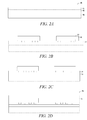
- FIG. 1 is a stylized side profile of a semiconductor device.
- FIGS. 2 a -2 g an exemplary sequential process flow for making a semiconductor device.
- FIG. 3 is a flow chart for making the semiconductor device in accordance with some embodiments.
- FIG. 4 is a block diagram of an electronic device incorporating at least one chip with at least one electrical interconnect in accordance with some embodiments.
- Certain semiconductor devices may incorporate a bonding layer.
- a molding process and/or a wafer-level underfill process may apply the bonding layer by flowing the bonding layer between and among the electrical contacts of a chip.
- flowing the bonding layer may result in inconsistent application of the bonding layer and potentially undesirable stresses on the electrical contacts, such as when the bonding layer is cured.
- a semiconductor device that incorporates multiple chips may have an anticipated alignment accuracy between the chips and the electrical connections of the chips of approximately fifteen (15) micrometers.
- processes that incorporate relatively fine lines in the distribution circuitry such as approximately two (2) micrometer lines and spaces between the lines, may be relatively unreliable between two chips in a single semiconductor device, given the discrepancy between the tolerance on chip positioning and the size of the lines and spaces.
- FIG. 1 is a side profile of a semiconductor device 100 .
- the semiconductor device 100 as illustrated includes two components 102 , such as a chip, a die, or other component, such as may be fabricated from silicon.
- the semiconductor device 100 may include only one chip 102 or more than two chips 102 .
- Each chip 102 includes at least one electrical contact 104 .
- Distribution circuitry 106 is coupled to the electrical contact 104 .
- a solder bump 108 is optionally coupled to the distribution circuitry 106 .
- the distribution circuitry 106 a optionally couples one electrical contact 104 a of one chip 102 to a second electrical contact 104 b of a second chip 102 . Taken together, the electrical contact 104 , the distribution circuitry 106 and the solder bump 108 provide input and output connectivity with the respective chips 102 .
- a molding layer 110 may provide general mechanical stability for the semiconductor device 100 as well as secure the chips 102 with respect to one another and the rest of the components of the semiconductor device 100 .
- a bonding layer 112 may provide mechanical stability for the electrical contacts 104 , and optionally the chips 102 and the distribution circuitry 106 .
- a buildup layer 114 may provide mechanical stability for the distribution circuitry 106 .
- the molding layer 110 , the bonding layer 112 , and the buildup layer 114 may combine to provide general mechanical stability for the semiconductor device 100 generally and any or all of the components of the semiconductor device 100 .
- the molding layer 110 may be a molding compound for use with semiconductor devices.
- the molding compound can include or be made of a material with a relatively very high filler content, such as a weight percentage of from sixty (60) to ninety (90) percent.
- the molding compound can include a mix of organic material such as epoxy and/or an inorganic filler, such as SiO 2 , SiC, and AlN.
- the bonding layer 112 may be the same or similar material as is used in wafer-level underfill processes.
- the buildup layer 114 may include a buildup material such as epoxy with filler, liquid crystal polymer, polyimide, SiO 2 , and other organic or inorganic dielectric materials.
- the molding layer 110 , bonding layer 112 , and buildup layer 114 may perform the same or similar functions.
- the bonding layer 112 of the semiconductor device 100 is not flowed around the electrical contacts 104 . Rather, the electrical contacts 104 and the chip 102 generally is pressed or otherwise inserted into the bonding layer 112 by a compression force before the bonding layer 112 has cured. Because the chip 102 or chips 102 are pressed into the bonding layer 112 , the relative position of the chips with respect to the bonding layer 112 may be relatively more precisely controlled than may be achieved through other bonding layer 112 application processes.
- the bonding layer 112 may produce lessened or differently-distributed stresses, such as on the electrical contacts 104 , than may be achieved with a wafer-level underfill process under certain circumstances. Additionally, the semiconductor device 100 generally may incorporate less warpage than may be achieved through wafer-level underfill, may enable bumped silicon, and may provide for increased positioning accuracy of the chip or chips 102 .
- FIGS. 2 a -2 g illustrate an exemplary sequential process flow for making the semiconductor device 100 .
- the building of the semiconductor device 100 is not limited only to the process flow of FIGS. 2 a -2 g , but rather may incorporate any of a variety of process steps that may produce the semiconductor device 100 .
- a carrier layer 200 may provide mechanical stability for the semiconductor device 100 , such as during the manufacturing process.
- the carrier layer 200 may be comprised of any of a variety of materials that have or may be utilized in the manufacture of semiconductor devices generally.
- the carrier layer 200 is comprised of stainless steel, glass, ceramic, silicon, and other similar or suitable materials.
- the adhesive layer 202 adheres the carrier layer 200 with respect to the bonding layer 112 .
- the adhesive layer 202 and the bonding layer 112 may together be provided as a die attach film 203 .
- the adhesive layer 202 may include a debondable adhesive.
- the debondable adhesive may be a thermo-releasable adhesive, a ultraviolet-releasable adhesive, a laser-releasable adhesive, a chemically-releasable adhesive, or other suitable debondable adhesive.
- the bonding layer 112 is an epoxy.
- the epoxy is a B-staged epoxy or a polyamide epoxy.
- the bonding layer is an SU-8 photoresist.
- the bonding layer 112 may include a filler that may provide additional mechanical strength.
- the thickness of the bonding layer 112 may be at least as great as the height of the electrical contact relative to the rest of the chip 102 . Alternatively or additionally, the thickness of the bonding layer 112 may be based on the size of other components of the semiconductor device 100 , such as the distribution circuitry 106 .
- the electrical contacts 104 of the chips 102 are pressed into the bonding layer 112 .
- the electrical contacts 104 may be inserted into the bonding layer 112 by compression. The insertion may be performed at room temperature.
- the bonding layer 112 may be heated to promote insertion of the electrical contacts 104 . Heating of the bonding layer 112 and the selection of the materials of the bonding layer 112 in general may be based, at least in part, a viscosity sufficient to admit the electrical contacts 104 while maintaining adequate opposing force on the electrical contacts.
- a portion of the chips 102 in addition to the electrical contacts 104 of the chips are pressed into the bonding layer 112 .
- the electrical contacts 104 are pressed into the bonding layer 112 only sufficiently to cover the electrical contacts 104 in the bonding layer 112 .
- a portion of the rest of the chips 102 may be pressed into the bonding layer 112 . Pressing a portion of the chips 102 into the bonding layer 112 in addition to the electrical contact 104 may increase an amount of the electrical contacts 104 that are covered by the bonding layer 112 and, in various examples, increase an extent to which the bonding layer 112 secures the chips 102 .
- the bonding layer 112 mechanically secures the chips 102 by creating a mechanical interface at least between the bonding layer 112 and the electrical interconnects 104 . In various examples, the bonding layer 112 alternatively or additionally adhesively secures the chips 102 by adhering with at least the electrical interconnects 104 .
- the bonding layer 112 is cured.
- the bonding layer 112 is cured by applying heat.
- the bonding layer 112 may be cured at a temperature less than a thermal breakdown temperature of the adhesive layer 202 , in examples where the adhesive layer 202 is thermo-releasable.
- the bonding layer 112 may be substantially fully cured, such as by reducing a reactivity of the material of the bonding layer 112 to less than one (1) percent.
- a bonding layer 112 into which the electrical interconnects 104 have been pressed may be identified by cross-linking free radicals in an organic resin on the bonding layer 112 from less than sixty (60) percent to over ninety-nine (99) percent.
- the molding layer 110 is applied to the semiconductor device 100 .
- the molding layer 110 is applied by pressure molding.
- the molding layer may be applied to an entire wafer or selectively to a portion of a wafer or particular semiconductor device 100 .
- the adhesive layer 202 is debonded and the carrier 200 removed. Debonding the adhesive layer 202 exposes a surface 206 of the bonding layer 112 .
- the surface 208 FIG. 2 f below of one or more electrical contacts 104 may also be exposed.
- the now-exposed surface 206 of the bonding layer 112 is planarized.
- the bonding layer 112 may be planarized to expose the surface 208 of the electrical contacts 104 .
- Planarization may expose all of the electrical contacts 104 and may provide substantially co-planar surfaces 208 of the electrical contacts 104 .
- Co-planarity of the surfaces 208 may be on the micron-level. Planarization may be achieved through grinding, polishing, or other methods.
- the semiconductor device 100 is built up by adding the distribution circuitry 106 , the buildup layer 114 , and the solder bumps 108 .
- the distribution circuitry 106 a connects at least one electrical contact 104 a to another electrical contact 104 b.
- FIG. 3 is a flowchart for producing a device, such as the semiconductor device 100 . It is noted that the flowchart is not limited only to making the semiconductor device 100 .
- the die attach film 203 is attached to the carrier layer 200 .
- the die attach film 203 includes the adhesive layer 202
- the die attach film 203 is attached to the carrier 200 by adhesively coupling the adhesive layer 202 to the carrier layer 200 .
- the adhesive layer 202 and bonding layer 112 may be separately and individually adhesively coupled with respect to the carrier layer 200 .
- the bonding layer 112 is cured.
- the bonding layer 112 is cured after the electrical contact 104 is pressed into the bonding layer 112 .
- the electrical contact 104 may be coupled, at least in part, to the bonding layer 112 .
- the coupling between the electrical contact 104 and the bonding layer 112 substantially secures the electrical contact 104 specifically and the chip 102 generally with respect to the bonding layer 112 so that the chip 102 does not move with respect to the bonding layer 112 under normal forces.
- the molding layer 110 may contribute to substantially securing the chip 102 with respect to the bonding layer 112 .
- a molding compound of the molding layer 110 is applied in contact with the chip 102 and a first major surface of the bonding layer 112 .
- the molding layer 110 may contribute mechanical rigidity to the semiconductor device 100 and may further secure the chip 102 with respect to the bonding layer 112 .
- the bonding layer 112 is planarized.
- the bonding layer 112 may be planarized by polishing, grinding, or other methods that would be apparent to one of ordinary skill in the art.
- the bonding layer 112 may be planarized until the contact surface 208 of the electrical contact 104 is exposed. Exposing the electrical contact 104 may be performed if the contact surface 208 is not already exposed.
- planarizing the bonding layer 112 further includes planarizing the electrical contact 104 or some or all of the electrical contacts 104 .
- the electrical contacts 104 may be planarized until the contact surfaces 208 of the electrical contacts 104 are substantially co-planar.
- the adhesive layer 202 is debonded.
- the adhesive layer 202 is debonded by applying a stimulant based on the nature of the adhesive layer 202 .
- debonding the adhesive layer 202 includes applying heat to the adhesive layer 202 .
- debonding the adhesive layer 202 includes applying ultra-violet energy to the adhesive layer 202 .
- the carrier layer 200 is removed from the semiconductor device 100 .
- the distribution circuitry 106 is coupled to the contact surface 208 of at least one of the electrical contacts 104 .
- the buildup layer 114 is applied to a second major surface of the bonding layer 112 opposite the first major surface.
- the buildup layer 114 may contribute to the mechanical rigidity of the semiconductor device 100 and substantially surround and provide mechanical support to the distribution circuitry 106 .
- FIG. 4 is a block diagram of an electronic device 400 incorporating at least semiconductor device 100 .
- the electronic device 400 is merely one example of an electronic system in which embodiments of the present disclosure may be used. Examples of electronic devices 400 include, but are not limited to personal computers, tablet computers, mobile telephones, personal data assistants, MP3 or other digital music players, etc.
- the electronic device 400 comprises a data processing system that includes a system bus 402 to couple the various components of the system.
- the system bus 402 provides communications links among the various components of the electronic device 400 and may be implemented as a single bus, as a combination of busses, or in any other suitable manner.
- circuits that may be included in the electronic assembly 410 are a custom circuit, an application-specific integrated circuit (ASIC), or the like, such as, for example, one or more circuits (such as a communications circuit 414 ) for use in wireless devices like mobile telephones, pagers, personal data assistants, portable computers, two-way radios, and similar electronic systems.
- ASIC application-specific integrated circuit
- the IC may perform any other type of function.
- the electronic device 400 may also include a display device 416 , one or more speakers 418 , and a keyboard and/or controller 430 , which may include a mouse, trackball, touch screen, voice-recognition device, or any other device that permits a system user to input information into and receive information from the electronic device 400 .
- Example 1 a method of making a semiconductor device comprises pressing an electrical contact of a chip into a bonding layer on a carrier, curing the bonding layer, wherein the bonding layer, as cured, is coupled, at least in part, to the electrical contact, applying a molding compound in contact with the chip and a first major surface of the bonding layer, and coupling distribution circuitry to the electrical contact.
- Example 2 the method of Example 1 optionally further comprises, prior to coupling the distribution circuitry, planarizing the bonding layer.
- Example 3 the method of any one or more of Examples 1 and 2 optionally planarizes the bonding layer by exposing a contact surface of the electrical contact, and coupling the distribution circuitry couples the distribution circuitry to the contact surface.
- Example 4 the method of any one or more of Examples 1-3 optionally planarizes the bonding layer by planarizing the electrical contact to expose the contact surface of the electrical contact.
- Example 5 the method of any one or more of Examples 1-4 optionally includes the chip comprising a plurality of electrical contacts, wherein pressing the electrical contact optionally comprises pressing the plurality of electrical contacts into the bonding layer, and planarizing the electrical contact optionally comprises planarizing the plurality of electrical contacts to make contact surfaces of the electrical contacts substantially co-planar.
- Example 6 the method of any one or more of Examples 1-5 optionally further comprises, prior to pressing the electrical contact into the bonding layer, attaching a die attach film to the carrier layer, the die attach film comprising the bonding layer and, prior to coupling the distribution circuitry, removing the carrier layer.
- Example 7 the method of any one or more of Examples 1-6 optionally includes the die attach film comprising an adhesive layer adhesively coupled to the bonding layer, and attaching the die attach film to the carrier layer optionally comprises adhesively coupling the adhesive layer to the carrier layer.
- Example 8 the method of any one or more of Examples 1-7 optionally includes the adhesive layer is comprised of a debondable adhesive, and the removing the carrier layer optionally comprises debonding the adhesive.
- Example 9 the method of any one or more of Examples 1-8 optionally includes that the debondable adhesive is one of a thermo-releasable adhesive and an ultra-violet-releasable adhesive, and debonding the adhesive optionally comprises applying at least one of heat and ultra-violet energy.
- the debondable adhesive is one of a thermo-releasable adhesive and an ultra-violet-releasable adhesive
- debonding the adhesive optionally comprises applying at least one of heat and ultra-violet energy.
- Example 10 the method of any one or more of Examples 1-9 optionally further comprises applying a buildup layer on a second major surface of the bonding layer opposite the first major surface and substantially surrounding the distribution circuitry.
- Example 11 the method of any one or more of Examples 1-10 optionally further comprises coupling solder bumps to the distribution circuitry, wherein the buildup layer secures, in part, the solder bumps.
- Example 12 may include subject matter (such as an apparatus, a method, a means for performing acts) that may include a semiconductor device, comprising a chip including an electrical contact, a cured bonding layer into which the electrical contact has been pressed and at least partially secured, a molding compound in contact with the chip and a first major surface of the bonding layer, and distribution circuitry electrically coupled to the electrical contact.
- a semiconductor device comprising a chip including an electrical contact, a cured bonding layer into which the electrical contact has been pressed and at least partially secured, a molding compound in contact with the chip and a first major surface of the bonding layer, and distribution circuitry electrically coupled to the electrical contact.
- Example 13 the device of Example 12 optionally comprises a plurality of electrical contacts each having been pressed into the bonding layer, wherein the plurality of electrical contacts are substantially co-planar.
- Example 14 the device of any one or more of Examples 12 and 13 optionally includes that the chip is a first chip and that the semiconductor device optionally further comprises a second chip including an electrical contact that has been pressed into the bonding layer, wherein the distribution circuitry electrically couples the electrical contact of the first chip to the electrical contact of the second chip.
- Example 15 the device of any one or more of Examples 12-14 optionally includes that the electrical contacts have been pressed into the bonding layer to a substantially similar depth of the bonding layer.
- Example 16 may include subject matter (such as an apparatus, a method, a means for performing acts) that may include a semiconductor device, comprising a carrier layer, a substantially uncured bonding layer, a debondable adhesive layer positioned between the carrier layer and the bonding layer, the carrier layer and the bonding layer being adhesively coupled to the adhesive layer, and a chip comprising an electrical contact pressed into the bonding layer.
- a semiconductor device comprising a carrier layer, a substantially uncured bonding layer, a debondable adhesive layer positioned between the carrier layer and the bonding layer, the carrier layer and the bonding layer being adhesively coupled to the adhesive layer, and a chip comprising an electrical contact pressed into the bonding layer.
- Example 17 the device of Example 16 optionally includes that the adhesive layer is configured to release the carrier layer with respect to the bonding layer upon the adhesive layer being debonded.
- Example 18 the device of any one or more of Examples 16 and 17 optionally includes that the debondable adhesive layer comprises one of a thermo-releasable adhesive and an ultra-violet-releasable adhesive, and wherein the adhesive layer is debonded upon application of at least one of heat and ultra-violet energy.
- the debondable adhesive layer comprises one of a thermo-releasable adhesive and an ultra-violet-releasable adhesive, and wherein the adhesive layer is debonded upon application of at least one of heat and ultra-violet energy.
- Example 19 the device of any one or more of Examples 16-18 optionally includes that the chip comprises a plurality of electrical contacts each having been pressed into the bonding layer.
- Example 20 the device of any one or more of Examples 16-19 optionally includes that the bonding layer is a polyamide epoxy.
- the terms “a” or “an” are used, as is common in patent documents, to include one or more than one, independent of any other instances or usages of “at least one” or “one or more.”
- the term “or” is used to refer to a nonexclusive or, such that “A or B” includes “A but not B,” “B but not A,” and “A and B,” unless otherwise indicated.
Landscapes
- Engineering & Computer Science (AREA)
- Computer Hardware Design (AREA)
- Microelectronics & Electronic Packaging (AREA)
- Power Engineering (AREA)
- Physics & Mathematics (AREA)
- Condensed Matter Physics & Semiconductors (AREA)
- General Physics & Mathematics (AREA)
- Manufacturing & Machinery (AREA)
- Wire Bonding (AREA)
Abstract
Description
Claims (11)
Priority Applications (1)
| Application Number | Priority Date | Filing Date | Title |
|---|---|---|---|
| US14/493,718 US9659885B2 (en) | 2012-08-29 | 2014-09-23 | Semiconductor device with pre-molding chip bonding |
Applications Claiming Priority (2)
| Application Number | Priority Date | Filing Date | Title |
|---|---|---|---|
| US13/598,352 US8872355B2 (en) | 2012-08-29 | 2012-08-29 | Semiconductor device with pre-molding chip bonding |
| US14/493,718 US9659885B2 (en) | 2012-08-29 | 2014-09-23 | Semiconductor device with pre-molding chip bonding |
Related Parent Applications (1)
| Application Number | Title | Priority Date | Filing Date |
|---|---|---|---|
| US13/598,352 Division US8872355B2 (en) | 2012-08-29 | 2012-08-29 | Semiconductor device with pre-molding chip bonding |
Publications (2)
| Publication Number | Publication Date |
|---|---|
| US20150008595A1 US20150008595A1 (en) | 2015-01-08 |
| US9659885B2 true US9659885B2 (en) | 2017-05-23 |
Family
ID=50186375
Family Applications (2)
| Application Number | Title | Priority Date | Filing Date |
|---|---|---|---|
| US13/598,352 Active US8872355B2 (en) | 2012-08-29 | 2012-08-29 | Semiconductor device with pre-molding chip bonding |
| US14/493,718 Active US9659885B2 (en) | 2012-08-29 | 2014-09-23 | Semiconductor device with pre-molding chip bonding |
Family Applications Before (1)
| Application Number | Title | Priority Date | Filing Date |
|---|---|---|---|
| US13/598,352 Active US8872355B2 (en) | 2012-08-29 | 2012-08-29 | Semiconductor device with pre-molding chip bonding |
Country Status (1)
| Country | Link |
|---|---|
| US (2) | US8872355B2 (en) |
Families Citing this family (6)
| Publication number | Priority date | Publication date | Assignee | Title |
|---|---|---|---|---|
| US8872355B2 (en) | 2012-08-29 | 2014-10-28 | Intel Corporation | Semiconductor device with pre-molding chip bonding |
| US10515927B2 (en) * | 2017-04-21 | 2019-12-24 | Applied Materials, Inc. | Methods and apparatus for semiconductor package processing |
| CN107452702A (en) * | 2017-07-28 | 2017-12-08 | 中芯长电半导体(江阴)有限公司 | The encapsulating structure and method for packing of semiconductor chip |
| US10181449B1 (en) * | 2017-09-28 | 2019-01-15 | Taiwan Semiconductor Manufacturing Co., Ltd. | Semiconductor structure |
| US10629559B2 (en) * | 2018-09-19 | 2020-04-21 | Powertech Technology Inc. | Semiconductor package and manufacturing method thereof |
| TWI691204B (en) * | 2018-12-22 | 2020-04-11 | 弘真科技股份有限公司 | A wireless audiovisual information sharing system and method |
Citations (5)
| Publication number | Priority date | Publication date | Assignee | Title |
|---|---|---|---|---|
| US20090045513A1 (en) * | 2007-08-17 | 2009-02-19 | Samsung Electronics Co., Ltd. | Semiconductor chip package, electronic device including the semiconductor chip package and methods of fabricating the electronic device |
| US20100019368A1 (en) * | 2008-07-25 | 2010-01-28 | Samsung Electronics Co., Ltd. | Semiconductor chip package, stacked package comprising semiconductor chips and methods of fabricating chip and stacked packages |
| US20100133680A1 (en) | 2008-12-03 | 2010-06-03 | Samsung Electro-Mechanics Co., Ltd. | Wafer level package and method of manufacturing the same and method of reusing chip |
| US20110001247A1 (en) * | 2009-07-01 | 2011-01-06 | Casio Computer Co., Ltd. | Semiconductor device manufacturing method |
| US20140061954A1 (en) | 2012-08-29 | 2014-03-06 | Chuan Hu | Semiconductor device with pre-molding chip bonding |
-
2012
- 2012-08-29 US US13/598,352 patent/US8872355B2/en active Active
-
2014
- 2014-09-23 US US14/493,718 patent/US9659885B2/en active Active
Patent Citations (6)
| Publication number | Priority date | Publication date | Assignee | Title |
|---|---|---|---|---|
| US20090045513A1 (en) * | 2007-08-17 | 2009-02-19 | Samsung Electronics Co., Ltd. | Semiconductor chip package, electronic device including the semiconductor chip package and methods of fabricating the electronic device |
| US20100019368A1 (en) * | 2008-07-25 | 2010-01-28 | Samsung Electronics Co., Ltd. | Semiconductor chip package, stacked package comprising semiconductor chips and methods of fabricating chip and stacked packages |
| US20100133680A1 (en) | 2008-12-03 | 2010-06-03 | Samsung Electro-Mechanics Co., Ltd. | Wafer level package and method of manufacturing the same and method of reusing chip |
| US20110001247A1 (en) * | 2009-07-01 | 2011-01-06 | Casio Computer Co., Ltd. | Semiconductor device manufacturing method |
| US20140061954A1 (en) | 2012-08-29 | 2014-03-06 | Chuan Hu | Semiconductor device with pre-molding chip bonding |
| US8872355B2 (en) | 2012-08-29 | 2014-10-28 | Intel Corporation | Semiconductor device with pre-molding chip bonding |
Non-Patent Citations (7)
Also Published As
| Publication number | Publication date |
|---|---|
| US8872355B2 (en) | 2014-10-28 |
| US20140061954A1 (en) | 2014-03-06 |
| US20150008595A1 (en) | 2015-01-08 |
Similar Documents
| Publication | Publication Date | Title |
|---|---|---|
| US9659885B2 (en) | Semiconductor device with pre-molding chip bonding | |
| KR101141493B1 (en) | Resin varnish used for adhesive film for semiconductor element, adhesive film for semiconductor element, and semiconductor device | |
| TWI306423B (en) | Method for bonding between electrical devices using ultrasonic vibration | |
| KR101856914B1 (en) | Film adhesive, semiconductor package using film adhesive and method for manufacturing same | |
| US9190381B2 (en) | Connection method, connection structure, insulating adhesive member, electronic component having adhesive member, and method for manufacturing same | |
| KR101023844B1 (en) | Adhesive resin composition, adhesive film, dicing die bonding film and semiconductor device using the same | |
| US9155191B2 (en) | Substrate comprising inorganic material that lowers the coefficient of thermal expansion (CTE) and reduces warpage | |
| SG148877A1 (en) | Semiconductor substrates including input/output redistribution using wire bonds and anisotropically conductive film, methods of fabrication and assemblies including same | |
| WO2017166325A1 (en) | Semiconductor package with supported stacked die | |
| US10741534B2 (en) | Multi-die microelectronic device with integral heat spreader | |
| US20140131897A1 (en) | Warpage Control for Flexible Substrates | |
| US11676900B2 (en) | Electronic assembly that includes a bridge | |
| JP2017108189A (en) | Package having dielectric or anisotropic conductive film (acf) build-up layer | |
| JP5710098B2 (en) | Manufacturing method of semiconductor device | |
| US9520378B2 (en) | Thermal matched composite die | |
| US10629557B2 (en) | Improving mechanical and thermal reliability in varying form factors | |
| Suk et al. | Flexible Chip-on-Flex (COF) and embedded Chip-in-Flex (CIF) packages by applying wafer level package (WLP) technology using anisotropic conductive films (ACFs) | |
| US9859249B2 (en) | Method of fabricating an electronic package | |
| US9324680B2 (en) | Solder attach apparatus and method | |
| US20160172229A1 (en) | Stiffener tape for electronic assembly | |
| WO2015119095A1 (en) | Anisotropic conductive film and method for producing same | |
| US9349698B2 (en) | Integrated WLUF and SOD process | |
| US11676876B2 (en) | Semiconductor die package with warpage management and process for forming such | |
| JP2009260213A (en) | Method of manufacturing semiconductor device | |
| Cheng et al. | A Novel Multifunctional Single-Layer Adhesive Used for both Temporary Bonding and Mechanical Debonding in Wafer-Level Packaging Applications |
Legal Events
| Date | Code | Title | Description |
|---|---|---|---|
| FEPP | Fee payment procedure |
Free format text: PAYOR NUMBER ASSIGNED (ORIGINAL EVENT CODE: ASPN); ENTITY STATUS OF PATENT OWNER: LARGE ENTITY |
|
| STCF | Information on status: patent grant |
Free format text: PATENTED CASE |
|
| MAFP | Maintenance fee payment |
Free format text: PAYMENT OF MAINTENANCE FEE, 4TH YEAR, LARGE ENTITY (ORIGINAL EVENT CODE: M1551); ENTITY STATUS OF PATENT OWNER: LARGE ENTITY Year of fee payment: 4 |
|
| AS | Assignment |
Owner name: TAHOE RESEARCH, LTD., IRELAND Free format text: ASSIGNMENT OF ASSIGNORS INTEREST;ASSIGNOR:INTEL CORPORATION;REEL/FRAME:061175/0176 Effective date: 20220718 |