US9640611B2 - HV complementary bipolar transistors with lateral collectors on SOI with resurf regions under buried oxide - Google Patents
HV complementary bipolar transistors with lateral collectors on SOI with resurf regions under buried oxide Download PDFInfo
- Publication number
- US9640611B2 US9640611B2 US14/219,760 US201414219760A US9640611B2 US 9640611 B2 US9640611 B2 US 9640611B2 US 201414219760 A US201414219760 A US 201414219760A US 9640611 B2 US9640611 B2 US 9640611B2
- Authority
- US
- United States
- Prior art keywords
- type
- layer
- region
- pnp
- box
- Prior art date
- Legal status (The legal status is an assumption and is not a legal conclusion. Google has not performed a legal analysis and makes no representation as to the accuracy of the status listed.)
- Active, expires
Links
- 230000000295 complement effect Effects 0.000 title abstract description 6
- 239000012212 insulator Substances 0.000 claims abstract description 23
- 229910021420 polycrystalline silicon Inorganic materials 0.000 claims abstract description 20
- 239000000758 substrate Substances 0.000 claims abstract description 17
- 229920005591 polysilicon Polymers 0.000 claims 2
- 239000012535 impurity Substances 0.000 abstract description 10
- 238000000034 method Methods 0.000 abstract description 8
- XUIMIQQOPSSXEZ-UHFFFAOYSA-N Silicon Chemical compound [Si] XUIMIQQOPSSXEZ-UHFFFAOYSA-N 0.000 abstract description 3
- 229910052710 silicon Inorganic materials 0.000 abstract description 3
- 239000010703 silicon Substances 0.000 abstract description 3
- 239000004065 semiconductor Substances 0.000 description 16
- 230000000873 masking effect Effects 0.000 description 11
- 230000008021 deposition Effects 0.000 description 8
- 239000007943 implant Substances 0.000 description 7
- 229910021421 monocrystalline silicon Inorganic materials 0.000 description 5
- 230000015556 catabolic process Effects 0.000 description 4
- 238000005516 engineering process Methods 0.000 description 4
- 238000005530 etching Methods 0.000 description 4
- 238000004519 manufacturing process Methods 0.000 description 4
- 150000004767 nitrides Chemical class 0.000 description 4
- 230000003647 oxidation Effects 0.000 description 4
- 238000007254 oxidation reaction Methods 0.000 description 4
- VYPSYNLAJGMNEJ-UHFFFAOYSA-N Silicium dioxide Chemical compound O=[Si]=O VYPSYNLAJGMNEJ-UHFFFAOYSA-N 0.000 description 2
- 229910000577 Silicon-germanium Inorganic materials 0.000 description 2
- 239000000463 material Substances 0.000 description 2
- 238000010276 construction Methods 0.000 description 1
- 230000003247 decreasing effect Effects 0.000 description 1
- 239000010432 diamond Substances 0.000 description 1
- 238000009413 insulation Methods 0.000 description 1
- 230000003071 parasitic effect Effects 0.000 description 1
- 235000012239 silicon dioxide Nutrition 0.000 description 1
- 239000000377 silicon dioxide Substances 0.000 description 1
Images


Classifications
-
- H—ELECTRICITY
- H01—ELECTRIC ELEMENTS
- H01L—SEMICONDUCTOR DEVICES NOT COVERED BY CLASS H10
- H01L27/00—Devices consisting of a plurality of semiconductor or other solid-state components formed in or on a common substrate
- H01L27/02—Devices consisting of a plurality of semiconductor or other solid-state components formed in or on a common substrate including semiconductor components specially adapted for rectifying, oscillating, amplifying or switching and having potential barriers; including integrated passive circuit elements having potential barriers
- H01L27/12—Devices consisting of a plurality of semiconductor or other solid-state components formed in or on a common substrate including semiconductor components specially adapted for rectifying, oscillating, amplifying or switching and having potential barriers; including integrated passive circuit elements having potential barriers the substrate being other than a semiconductor body, e.g. an insulating body
- H01L27/1203—Devices consisting of a plurality of semiconductor or other solid-state components formed in or on a common substrate including semiconductor components specially adapted for rectifying, oscillating, amplifying or switching and having potential barriers; including integrated passive circuit elements having potential barriers the substrate being other than a semiconductor body, e.g. an insulating body the substrate comprising an insulating body on a semiconductor body, e.g. SOI
-
- H—ELECTRICITY
- H01—ELECTRIC ELEMENTS
- H01L—SEMICONDUCTOR DEVICES NOT COVERED BY CLASS H10
- H01L23/00—Details of semiconductor or other solid state devices
- H01L23/52—Arrangements for conducting electric current within the device in operation from one component to another, i.e. interconnections, e.g. wires, lead frames
- H01L23/535—Arrangements for conducting electric current within the device in operation from one component to another, i.e. interconnections, e.g. wires, lead frames including internal interconnections, e.g. cross-under constructions
-
- H—ELECTRICITY
- H01—ELECTRIC ELEMENTS
- H01L—SEMICONDUCTOR DEVICES NOT COVERED BY CLASS H10
- H01L27/00—Devices consisting of a plurality of semiconductor or other solid-state components formed in or on a common substrate
- H01L27/02—Devices consisting of a plurality of semiconductor or other solid-state components formed in or on a common substrate including semiconductor components specially adapted for rectifying, oscillating, amplifying or switching and having potential barriers; including integrated passive circuit elements having potential barriers
- H01L27/04—Devices consisting of a plurality of semiconductor or other solid-state components formed in or on a common substrate including semiconductor components specially adapted for rectifying, oscillating, amplifying or switching and having potential barriers; including integrated passive circuit elements having potential barriers the substrate being a semiconductor body
- H01L27/08—Devices consisting of a plurality of semiconductor or other solid-state components formed in or on a common substrate including semiconductor components specially adapted for rectifying, oscillating, amplifying or switching and having potential barriers; including integrated passive circuit elements having potential barriers the substrate being a semiconductor body including only semiconductor components of a single kind
- H01L27/082—Devices consisting of a plurality of semiconductor or other solid-state components formed in or on a common substrate including semiconductor components specially adapted for rectifying, oscillating, amplifying or switching and having potential barriers; including integrated passive circuit elements having potential barriers the substrate being a semiconductor body including only semiconductor components of a single kind including bipolar components only
-
- H—ELECTRICITY
- H01—ELECTRIC ELEMENTS
- H01L—SEMICONDUCTOR DEVICES NOT COVERED BY CLASS H10
- H01L29/00—Semiconductor devices specially adapted for rectifying, amplifying, oscillating or switching and having potential barriers; Capacitors or resistors having potential barriers, e.g. a PN-junction depletion layer or carrier concentration layer; Details of semiconductor bodies or of electrodes thereof ; Multistep manufacturing processes therefor
- H01L29/02—Semiconductor bodies ; Multistep manufacturing processes therefor
- H01L29/06—Semiconductor bodies ; Multistep manufacturing processes therefor characterised by their shape; characterised by the shapes, relative sizes, or dispositions of the semiconductor regions ; characterised by the concentration or distribution of impurities within semiconductor regions
- H01L29/0603—Semiconductor bodies ; Multistep manufacturing processes therefor characterised by their shape; characterised by the shapes, relative sizes, or dispositions of the semiconductor regions ; characterised by the concentration or distribution of impurities within semiconductor regions characterised by particular constructional design considerations, e.g. for preventing surface leakage, for controlling electric field concentration or for internal isolations regions
- H01L29/0607—Semiconductor bodies ; Multistep manufacturing processes therefor characterised by their shape; characterised by the shapes, relative sizes, or dispositions of the semiconductor regions ; characterised by the concentration or distribution of impurities within semiconductor regions characterised by particular constructional design considerations, e.g. for preventing surface leakage, for controlling electric field concentration or for internal isolations regions for preventing surface leakage or controlling electric field concentration
- H01L29/0611—Semiconductor bodies ; Multistep manufacturing processes therefor characterised by their shape; characterised by the shapes, relative sizes, or dispositions of the semiconductor regions ; characterised by the concentration or distribution of impurities within semiconductor regions characterised by particular constructional design considerations, e.g. for preventing surface leakage, for controlling electric field concentration or for internal isolations regions for preventing surface leakage or controlling electric field concentration for increasing or controlling the breakdown voltage of reverse biased devices
- H01L29/0615—Semiconductor bodies ; Multistep manufacturing processes therefor characterised by their shape; characterised by the shapes, relative sizes, or dispositions of the semiconductor regions ; characterised by the concentration or distribution of impurities within semiconductor regions characterised by particular constructional design considerations, e.g. for preventing surface leakage, for controlling electric field concentration or for internal isolations regions for preventing surface leakage or controlling electric field concentration for increasing or controlling the breakdown voltage of reverse biased devices by the doping profile or the shape or the arrangement of the PN junction, or with supplementary regions, e.g. junction termination extension [JTE]
- H01L29/063—Reduced surface field [RESURF] pn-junction structures
- H01L29/0634—Multiple reduced surface field (multi-RESURF) structures, e.g. double RESURF, charge compensation, cool, superjunction (SJ), 3D-RESURF, composite buffer (CB) structures
-
- H—ELECTRICITY
- H01—ELECTRIC ELEMENTS
- H01L—SEMICONDUCTOR DEVICES NOT COVERED BY CLASS H10
- H01L29/00—Semiconductor devices specially adapted for rectifying, amplifying, oscillating or switching and having potential barriers; Capacitors or resistors having potential barriers, e.g. a PN-junction depletion layer or carrier concentration layer; Details of semiconductor bodies or of electrodes thereof ; Multistep manufacturing processes therefor
- H01L29/02—Semiconductor bodies ; Multistep manufacturing processes therefor
- H01L29/06—Semiconductor bodies ; Multistep manufacturing processes therefor characterised by their shape; characterised by the shapes, relative sizes, or dispositions of the semiconductor regions ; characterised by the concentration or distribution of impurities within semiconductor regions
- H01L29/0603—Semiconductor bodies ; Multistep manufacturing processes therefor characterised by their shape; characterised by the shapes, relative sizes, or dispositions of the semiconductor regions ; characterised by the concentration or distribution of impurities within semiconductor regions characterised by particular constructional design considerations, e.g. for preventing surface leakage, for controlling electric field concentration or for internal isolations regions
- H01L29/0642—Isolation within the component, i.e. internal isolation
- H01L29/0649—Dielectric regions, e.g. SiO2 regions, air gaps
-
- H—ELECTRICITY
- H01—ELECTRIC ELEMENTS
- H01L—SEMICONDUCTOR DEVICES NOT COVERED BY CLASS H10
- H01L29/00—Semiconductor devices specially adapted for rectifying, amplifying, oscillating or switching and having potential barriers; Capacitors or resistors having potential barriers, e.g. a PN-junction depletion layer or carrier concentration layer; Details of semiconductor bodies or of electrodes thereof ; Multistep manufacturing processes therefor
- H01L29/02—Semiconductor bodies ; Multistep manufacturing processes therefor
- H01L29/06—Semiconductor bodies ; Multistep manufacturing processes therefor characterised by their shape; characterised by the shapes, relative sizes, or dispositions of the semiconductor regions ; characterised by the concentration or distribution of impurities within semiconductor regions
- H01L29/0684—Semiconductor bodies ; Multistep manufacturing processes therefor characterised by their shape; characterised by the shapes, relative sizes, or dispositions of the semiconductor regions ; characterised by the concentration or distribution of impurities within semiconductor regions characterised by the shape, relative sizes or dispositions of the semiconductor regions or junctions between the regions
- H01L29/0692—Surface layout
-
- H—ELECTRICITY
- H01—ELECTRIC ELEMENTS
- H01L—SEMICONDUCTOR DEVICES NOT COVERED BY CLASS H10
- H01L29/00—Semiconductor devices specially adapted for rectifying, amplifying, oscillating or switching and having potential barriers; Capacitors or resistors having potential barriers, e.g. a PN-junction depletion layer or carrier concentration layer; Details of semiconductor bodies or of electrodes thereof ; Multistep manufacturing processes therefor
- H01L29/02—Semiconductor bodies ; Multistep manufacturing processes therefor
- H01L29/06—Semiconductor bodies ; Multistep manufacturing processes therefor characterised by their shape; characterised by the shapes, relative sizes, or dispositions of the semiconductor regions ; characterised by the concentration or distribution of impurities within semiconductor regions
- H01L29/08—Semiconductor bodies ; Multistep manufacturing processes therefor characterised by their shape; characterised by the shapes, relative sizes, or dispositions of the semiconductor regions ; characterised by the concentration or distribution of impurities within semiconductor regions with semiconductor regions connected to an electrode carrying current to be rectified, amplified or switched and such electrode being part of a semiconductor device which comprises three or more electrodes
- H01L29/0804—Emitter regions of bipolar transistors
- H01L29/0808—Emitter regions of bipolar transistors of lateral transistors
-
- H—ELECTRICITY
- H01—ELECTRIC ELEMENTS
- H01L—SEMICONDUCTOR DEVICES NOT COVERED BY CLASS H10
- H01L29/00—Semiconductor devices specially adapted for rectifying, amplifying, oscillating or switching and having potential barriers; Capacitors or resistors having potential barriers, e.g. a PN-junction depletion layer or carrier concentration layer; Details of semiconductor bodies or of electrodes thereof ; Multistep manufacturing processes therefor
- H01L29/02—Semiconductor bodies ; Multistep manufacturing processes therefor
- H01L29/06—Semiconductor bodies ; Multistep manufacturing processes therefor characterised by their shape; characterised by the shapes, relative sizes, or dispositions of the semiconductor regions ; characterised by the concentration or distribution of impurities within semiconductor regions
- H01L29/08—Semiconductor bodies ; Multistep manufacturing processes therefor characterised by their shape; characterised by the shapes, relative sizes, or dispositions of the semiconductor regions ; characterised by the concentration or distribution of impurities within semiconductor regions with semiconductor regions connected to an electrode carrying current to be rectified, amplified or switched and such electrode being part of a semiconductor device which comprises three or more electrodes
- H01L29/0821—Collector regions of bipolar transistors
-
- H—ELECTRICITY
- H01—ELECTRIC ELEMENTS
- H01L—SEMICONDUCTOR DEVICES NOT COVERED BY CLASS H10
- H01L29/00—Semiconductor devices specially adapted for rectifying, amplifying, oscillating or switching and having potential barriers; Capacitors or resistors having potential barriers, e.g. a PN-junction depletion layer or carrier concentration layer; Details of semiconductor bodies or of electrodes thereof ; Multistep manufacturing processes therefor
- H01L29/02—Semiconductor bodies ; Multistep manufacturing processes therefor
- H01L29/06—Semiconductor bodies ; Multistep manufacturing processes therefor characterised by their shape; characterised by the shapes, relative sizes, or dispositions of the semiconductor regions ; characterised by the concentration or distribution of impurities within semiconductor regions
- H01L29/10—Semiconductor bodies ; Multistep manufacturing processes therefor characterised by their shape; characterised by the shapes, relative sizes, or dispositions of the semiconductor regions ; characterised by the concentration or distribution of impurities within semiconductor regions with semiconductor regions connected to an electrode not carrying current to be rectified, amplified or switched and such electrode being part of a semiconductor device which comprises three or more electrodes
- H01L29/1004—Base region of bipolar transistors
- H01L29/1008—Base region of bipolar transistors of lateral transistors
-
- H—ELECTRICITY
- H01—ELECTRIC ELEMENTS
- H01L—SEMICONDUCTOR DEVICES NOT COVERED BY CLASS H10
- H01L29/00—Semiconductor devices specially adapted for rectifying, amplifying, oscillating or switching and having potential barriers; Capacitors or resistors having potential barriers, e.g. a PN-junction depletion layer or carrier concentration layer; Details of semiconductor bodies or of electrodes thereof ; Multistep manufacturing processes therefor
- H01L29/66—Types of semiconductor device ; Multistep manufacturing processes therefor
- H01L29/66007—Multistep manufacturing processes
- H01L29/66075—Multistep manufacturing processes of devices having semiconductor bodies comprising group 14 or group 13/15 materials
- H01L29/66227—Multistep manufacturing processes of devices having semiconductor bodies comprising group 14 or group 13/15 materials the devices being controllable only by the electric current supplied or the electric potential applied, to an electrode which does not carry the current to be rectified, amplified or switched, e.g. three-terminal devices
- H01L29/66234—Bipolar junction transistors [BJT]
- H01L29/66265—Thin film bipolar transistors
-
- H—ELECTRICITY
- H01—ELECTRIC ELEMENTS
- H01L—SEMICONDUCTOR DEVICES NOT COVERED BY CLASS H10
- H01L29/00—Semiconductor devices specially adapted for rectifying, amplifying, oscillating or switching and having potential barriers; Capacitors or resistors having potential barriers, e.g. a PN-junction depletion layer or carrier concentration layer; Details of semiconductor bodies or of electrodes thereof ; Multistep manufacturing processes therefor
- H01L29/66—Types of semiconductor device ; Multistep manufacturing processes therefor
- H01L29/66007—Multistep manufacturing processes
- H01L29/66075—Multistep manufacturing processes of devices having semiconductor bodies comprising group 14 or group 13/15 materials
- H01L29/66227—Multistep manufacturing processes of devices having semiconductor bodies comprising group 14 or group 13/15 materials the devices being controllable only by the electric current supplied or the electric potential applied, to an electrode which does not carry the current to be rectified, amplified or switched, e.g. three-terminal devices
- H01L29/66234—Bipolar junction transistors [BJT]
- H01L29/66272—Silicon vertical transistors
-
- H—ELECTRICITY
- H01—ELECTRIC ELEMENTS
- H01L—SEMICONDUCTOR DEVICES NOT COVERED BY CLASS H10
- H01L29/00—Semiconductor devices specially adapted for rectifying, amplifying, oscillating or switching and having potential barriers; Capacitors or resistors having potential barriers, e.g. a PN-junction depletion layer or carrier concentration layer; Details of semiconductor bodies or of electrodes thereof ; Multistep manufacturing processes therefor
- H01L29/66—Types of semiconductor device ; Multistep manufacturing processes therefor
- H01L29/68—Types of semiconductor device ; Multistep manufacturing processes therefor controllable by only the electric current supplied, or only the electric potential applied, to an electrode which does not carry the current to be rectified, amplified or switched
- H01L29/70—Bipolar devices
- H01L29/72—Transistor-type devices, i.e. able to continuously respond to applied control signals
- H01L29/73—Bipolar junction transistors
- H01L29/732—Vertical transistors
-
- H—ELECTRICITY
- H01—ELECTRIC ELEMENTS
- H01L—SEMICONDUCTOR DEVICES NOT COVERED BY CLASS H10
- H01L29/00—Semiconductor devices specially adapted for rectifying, amplifying, oscillating or switching and having potential barriers; Capacitors or resistors having potential barriers, e.g. a PN-junction depletion layer or carrier concentration layer; Details of semiconductor bodies or of electrodes thereof ; Multistep manufacturing processes therefor
- H01L29/66—Types of semiconductor device ; Multistep manufacturing processes therefor
- H01L29/68—Types of semiconductor device ; Multistep manufacturing processes therefor controllable by only the electric current supplied, or only the electric potential applied, to an electrode which does not carry the current to be rectified, amplified or switched
- H01L29/70—Bipolar devices
- H01L29/72—Transistor-type devices, i.e. able to continuously respond to applied control signals
- H01L29/73—Bipolar junction transistors
- H01L29/735—Lateral transistors
Definitions
- This invention is in the field of bipolar transistor fabrication, and is more specifically directed to the fabrication of transistors having varying characteristics on a common substrate according to silicon-on-insulator (SOI) technology.
- SOI silicon-on-insulator
- bipolar transistors have utilized bipolar junction transistors for many years, taking advantage of their high gain characteristics to satisfy high performance and high current drive needs.
- bipolar transistors are especially well-suited for high frequency applications, such as now used in wireless communications.
- Silicon-on-insulator (SOI) technology is also well-known in the art as providing important advantages in high-frequency electronic devices.
- active devices such as transistors are formed in single-crystal silicon layers formed over an insulator layer, such as a layer of silicon dioxide commonly referred to as buried oxide (BOX).
- BOX buried oxide
- the buried oxide layer isolates the active devices from the underlying substrate, effectively eliminating parasitic nonlinear junction capacitances to the substrate and reducing collector-to-substrate capacitances.
- SOI technology provides significant improvement.
- SOI devices are robust in high voltage applications.
- the buried oxide layer effectively eliminates any reasonable possibility of junction breakdown to the substrate.
- a conventional SOI bipolar transistor is designed to be a high performance device.
- a high performance transistor is somewhat limited by its construction, from a standpoint of both breakdown voltage and performance.
- the collector emitter breakdown voltage (BVCEO) depends upon the thickness of collector region and upon the doping concentration of the collector region. Lighter doping of the collector region and a thicker collector region would increase this breakdown voltage.
- the emitter and base of a PNP is biased around the highest potential Vcc (relative to grounded substrate) while the collector is switched between Vcc and 0.
- High B-C bias corresponds to zero potential at collector.
- grounded p-substrate does not deplete lateral portion of collector region and, hence, does not help to increase BV.
- the emitter and base of an NPN is biased around the lowest potential GND (relative to grounded substrate) while the collector is switched between Vcc and 0.
- High B-C bias corresponds to VCC potential at collector.
- grounded p-substrate depletes lateral portion of collector region and, hence, helps to increase BV.
- an integrated circuit structure including both NPN and PNP high voltage transistors comprising: complementary PNP and NPN structures; wherein the PNP and NPN structures include an SOI semiconductor structure comprising: an p-type region; active PNP and NPN device regions; a buried insulator layer BOX that lies therebetween, touches, and electrically isolates p-type region from the active PNP and NPN regions; wherein both the p-type region and the active device PNP and NPN regions are implemented with single-crystal silicon; and an n-type region is included under the buried insulator layer BOX of the PNP transistor, by implanting donor impurities of through the active device region of the SOI wafer and BOX into the p-type region.
- FIG. 1 illustrates a cross-section of an embodiment of the present invention.
- FIG. 1A illustrates an enlarged portion of FIG. 1 detailing the NPN transistor.
- FIG. 1B illustrates an enlarged portion of FIG. 1 detailing the PNP transistor.
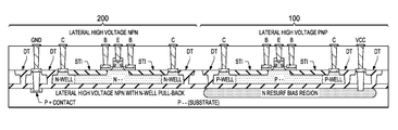
- FIG. 2 illustrates a cross-section of another embodiment of the present invention.
- FIG. 2A illustrates an enlarged portion of FIG. 2 detailing the NPN transistor.
- FIG. 2B illustrates an enlarged portion of FIG. 2 detailing the PNP transistor.
- FIG. 3 illustrates the calculated dependencies of BV CER on structures with no resurf and structures including resurf.
- the complementary PNP 100 and NPN 200 structures include an SOI semiconductor structure having an p-type region 101 , active device regions 104 and 204 respectively, and a buried insulator layer (BOX) 103 that lies therebetween, touches, and electrically isolates p-type region 101 from the active device regions 104 and 204 .
- the initial doping level of the active device regions 104 and 204 can be n-type, ⁇ 1e14 l/cm3.
- both the p-type region 101 and the active device regions 104 and 204 are implemented with single-crystal silicon.
- an n-type region 106 is included under the buried insulator layer (BOX) of the PNP transistor 100 , by implanting donor impurities with dose of about 1e13 to 1e14 l/cm2 through the active device region of the SOI wafer and BOX 103 (1.5-2 um in total) into p-type region 101 . Later in the process flow this n-type region 106 and the p-type regions 101 are connected from the top by doped poly-silicon plugs and are biased at Vcc and GND respectively. Since the substrate is p-type material, GND can be applied to either the p-type region 101 or the top contact GND. In this case it will deplete lateral portions of both the PNP and NPN collector regions and hence, will increase their BVs.
- BOX buried insulator layer
- the structure providing a PNP transistor 100 with a higher BV ( FIG. 1B ) is described below.
- a first masking and implant step is accomplished to create a highly ( ⁇ 1e17 l/cm3) doped n-layer 106 under BOX 103 in PNP area.
- the highly doped n-layer 106 is vertically under the PNP area and extends toward an n-type poly-silicon plug 110 and couples to that plug.
- a second masking and implant step after Pad Oxidation, before Nitride deposition is performed to create a uniform collector doping between 3e14-3e16 in active device region 104 .
- a Third masking and etching step is accomplished to provide a hard mask for defining and for deposition of an insulator layer STI 105 in the active device region 104 .
- Deep trenches 109 are formed to encircle the PNP transistor 100 and the n-type poly-silicon plug 110 .
- the trenches extend from the top of the die to the bottom of the BOX 103 and the n-type poly-silicon plug extends from the top of the die to and through the BOX 103 extending into the highly doped n-layer 106 under the BOX 103 , wherein the n-type poly-silicon plug touches the implanted n-layer under the BOX 103 and extends to the top of die providing a top contact to the implanted n-layer.
- a base epitaxial semiconductor layer 113 is deposited within an epitaxial layer 112 , defined and doped with an impurity of the opposite conductivity type on top of the active device region 104 with base contacts 111 coupled thereto.
- an emitter region 108 covers a portion of the base epitaxial semiconductor layer 113 , wherein the emitter region 108 is highly doped with the same conductivity type as the active device region 104 .
- the structure providing an NPN transistor 200 with a high BV FIG. 1A is described below.
- a first masking and implant step after Pad Oxidation, before Nitride deposition is performed to create a uniform collector doping between 3e14-3e16 l/cm3 in active device region 204 .
- a second masking and etching step is accomplished to provide a hard mask for defining and to for deposition of an insulator layer STI 105 in the active device region 204 .
- Deep trenches 109 are formed, to encircle the NPN 200 transistor and the p-type poly-silicon plug 210 .
- the trenches extend from the top of the die to the bottom of the BOX 103 and the p-type poly-silicon plug extends from the top of the die to and through the BOX 103 extending into the p-layer 101 under the BOX 103 , wherein the p-type poly-silicon plug touches the p-layer under the BOX 103 and extends to the top of die providing a top contact to the p-layer 101 .
- a base epitaxial semiconductor layer 213 is deposited, defined and doped with an impurity of the opposite conductivity type on top of the active device region 204 with base contacts 211 coupled thereto.
- an emitter region 208 covers a portion of the base epitaxial semiconductor layer 213 , wherein the emitter region 208 is highly doped with the same conductivity type as the first epitaxial layer 204 .
- the base epitaxial semiconductor for the NPN and the PNP can be either SiGe or silicon.
- the base epitaxial semiconductor can also be deposited in two operations, one for the NPN and one for the PNP.
- the complementary PNP 300 and NPN 400 structures include an SOI semiconductor structure having an n-type region 301 , active device regions 104 and 204 respectively, and a buried insulator layer (BOX) 103 that lies between, touches, and electrically isolates n-type region 301 from the active device regions 104 and 204 .
- the initial doping level of the active device regions 104 and 204 can be n-type, ⁇ 1e14 l/cm3.
- both the n-type region 301 and the active device regions 104 and 204 are implemented with single-crystal silicon.
- an n-type region 106 is included under a buried insulator layer (BOX) 103 of the PNP 300 transistor, by implanting donor impurity of about 2e15 to 1e17 through the active device region of the SOI wafer and BOX 103 (1.5-2 um in total) into n-type region 301 .
- a structure that yields higher NPN 400 BV includes p-type region 406 under the buried insulator layer (BOX) 103 of the NPN transistor, by implanting accepter impurities of about 2e15 to 1e17 through the active device region 204 of the SOI wafer and BOX 103 (1.5-2 um in total) into n-type region 301 .
- the n-type region 106 and the p-type regions 406 are connected from the top by doped poly-silicon plugs and are biased at Vcc and GND respectively. Since the substrate is n-type material, Vcc can be applied to either the n-type region 301 or the top contact Vcc. In this case it will deplete lateral portions of both the PNP and NPN collector regions and hence, will increase their BVs.
- a first masking and implant step is accomplished to create a highly ( ⁇ 1e17 l/cm3) doped n-layer 106 under BOX 103 in PNP area.
- the highly doped n-layer 106 is vertically under the PNP area and extends toward an n-type poly-silicon plug 110 and couples to that plug.
- a second new masking and implant step after Pad Oxidation, before Nitride deposition is performed to create a uniform collector doping between 3e14-3e16 in active device region 104 .
- a Third masking and etching step is accomplished to provide a hard mask for defining and to for deposition of a shallow trench insulation layer STI 105 in the active device region 104 .
- Deep trenches 109 are formed to encircle the PNP transistor 300 and the n-type poly-silicon plug 110 .
- the trenches extend from the top of the die to the bottom of the BOX 103 and the n-type poly-silicon plug 110 extends from the top of the die to and through the BOX 103 extending into the highly doped n-layer 106 under the BOX 103 , wherein the n-type poly-silicon plug 110 touches the implanted n-layer under the BOX 103 and extends to the top of die providing a top contact to the implanted n-layer 106 .
- a base epitaxial semiconductor layer 113 is deposited, defined and doped with an impurity of the opposite conductivity type on top of the active device region 104 with a base contact 111 coupled thereto.
- an emitter region 108 covers a portion of the base epitaxial semiconductor layer 113 , wherein the emitter region 108 is highly doped with the same conductivity type as the first epitaxial layer 104 .
- the structure providing an NPN transistor 400 with a high BV FIG. 1B is described below.
- a first masking and implant step is accomplished to create a highly ( ⁇ 1e17 l/cm3) doped p-layer 406 under BOX 103 in NPN area.
- the highly doped p-layer 106 is vertically under the NPN area and extends toward a p-type poly-silicon plug 210 and couples to that plug.
- a second new masking and implant step after Pad Oxidation, before Nitride deposition is performed to create a uniform collector doping between 3e14-3e16 l/cm3 in active device region 204 .
- a Third masking and etching step is accomplished to provide a hard mask for defining and to for deposition of an insulator layer STI 105 in the active device region 204 .
- Deep trenches 109 are formed, to encircle the NPN 400 transistor and the p-type poly-silicon plug 210 .
- the trenches extend from the top of the die to the bottom of the BOX 103 and the p-type poly-silicon plug 210 extends from the top of the die to and through the BOX 103 extending into the highly doped p-layer 406 under the BOX 103 , wherein the p-type poly-silicon plug 210 touches the implanted p-layer 406 under the BOX 103 and extends to the top of die providing a top contact to the implanted p-layer 406 .
- a base epitaxial semiconductor layer 213 is deposited, defined and doped with an impurity of the opposite conductivity type on top of the active device region 204 with base contacts 211 coupled thereto.
- an emitter region 208 covers a portion of the base epitaxial semiconductor layer 213 , wherein the emitter region 208 is highly doped with the same conductivity type as the first epitaxial layer 204 .
- the base epitaxial semiconductor for the NPN and the PNP can be either SiGe or silicon.
- the base epitaxial semiconductor can also be deposited in two operations, one for the NPN and one for the PNP.
Landscapes
- Engineering & Computer Science (AREA)
- Power Engineering (AREA)
- Microelectronics & Electronic Packaging (AREA)
- General Physics & Mathematics (AREA)
- Condensed Matter Physics & Semiconductors (AREA)
- Physics & Mathematics (AREA)
- Computer Hardware Design (AREA)
- Ceramic Engineering (AREA)
- Manufacturing & Machinery (AREA)
- Chemical & Material Sciences (AREA)
- Composite Materials (AREA)
- Bipolar Transistors (AREA)
- Bipolar Integrated Circuits (AREA)
Abstract
Complementary high-voltage bipolar transistors in silicon-on-insulator (SOI) integrated circuits is disclosed. In one disclosed embodiment, a collector region is formed in an epitaxial silicon layer disposed over a buried insulator layer. A base region and an emitter are disposed over the collector region. An n-type region is formed under the buried insulator layer (BOX) by implanting donor impurity through the active region of substrate and BOX into a p-substrate. Later in the process flow this n-type region is connected from the top by doped poly-silicon plug and is biased at Vcc. In this case it will deplete lateral portion of PNP collector region and hence, will increase its BV.
Description
This invention is in the field of bipolar transistor fabrication, and is more specifically directed to the fabrication of transistors having varying characteristics on a common substrate according to silicon-on-insulator (SOI) technology.
Integrated circuits have utilized bipolar junction transistors for many years, taking advantage of their high gain characteristics to satisfy high performance and high current drive needs. In particular, as is well known in the art, bipolar transistors are especially well-suited for high frequency applications, such as now used in wireless communications.
Silicon-on-insulator (SOI) technology is also well-known in the art as providing important advantages in high-frequency electronic devices. As is fundamental in SOI technology, active devices such as transistors are formed in single-crystal silicon layers formed over an insulator layer, such as a layer of silicon dioxide commonly referred to as buried oxide (BOX). The buried oxide layer isolates the active devices from the underlying substrate, effectively eliminating parasitic nonlinear junction capacitances to the substrate and reducing collector-to-substrate capacitances. To the extent that high frequency performance of bulk transistors was limited by substrate capacitance, SOI technology provides significant improvement.
In addition, SOI devices are robust in high voltage applications. The buried oxide layer effectively eliminates any reasonable possibility of junction breakdown to the substrate.
However it has been observed that those transistor features that facilitate high frequency performance tend to weaken the device from a high bias voltage standpoint, and vice versa. This tradeoff has typically been addressed by separately manufacturing high voltage integrated circuits and high performance integrated circuits, with each integrated circuit having transistors optimized for their particular implementation. This is because the process complexity resulting from integrating both high voltage and high performance devices in the same SOI integrated circuit adds significant cost and exerts manufacturing yield pressure.
A conventional SOI bipolar transistor is designed to be a high performance device. However, a high performance transistor is somewhat limited by its construction, from a standpoint of both breakdown voltage and performance. As is fundamental in the art, the collector emitter breakdown voltage (BVCEO) depends upon the thickness of collector region and upon the doping concentration of the collector region. Lighter doping of the collector region and a thicker collector region would increase this breakdown voltage.
In a real circuit, the emitter and base of a PNP is biased around the highest potential Vcc (relative to grounded substrate) while the collector is switched between Vcc and 0. High B-C bias corresponds to zero potential at collector. At this condition grounded p-substrate does not deplete lateral portion of collector region and, hence, does not help to increase BV.
The emitter and base of an NPN is biased around the lowest potential GND (relative to grounded substrate) while the collector is switched between Vcc and 0. High B-C bias corresponds to VCC potential at collector. At this condition grounded p-substrate depletes lateral portion of collector region and, hence, helps to increase BV.
What is needed is a method of increasing PNP BV without decreasing collector doping concentration or increasing collector region thickness of the PNP while including a high voltage NPN on the same circuit/substrate.
The following presents a simplified summary in order to provide a basic understanding of one or more aspects of the invention. This summary is not an extensive overview of the invention, and is neither intended to identify key or critical elements of the invention, nor to delineate the scope thereof. Rather, the primary purpose of the summary is to present some concepts of the invention in a simplified form as a prelude to a more detailed description that is presented later.
In accordance with an embodiment of the present application, an integrated circuit structure including both NPN and PNP high voltage transistors, the integrated circuit structure including both NPN and PNP high voltage transistors comprising: complementary PNP and NPN structures; wherein the PNP and NPN structures include an SOI semiconductor structure comprising: an p-type region; active PNP and NPN device regions; a buried insulator layer BOX that lies therebetween, touches, and electrically isolates p-type region from the active PNP and NPN regions; wherein both the p-type region and the active device PNP and NPN regions are implemented with single-crystal silicon; and an n-type region is included under the buried insulator layer BOX of the PNP transistor, by implanting donor impurities of through the active device region of the SOI wafer and BOX into the p-type region.
In accordance with another embodiment of the present application, an integrated circuit structure including both NPN and PNP high voltage transistors, the integrated circuit structure including both NPN and PNP high voltage transistors comprising: complementary PNP and NPN structures; wherein the PNP and NPN structures include an SOI semiconductor structure comprising: an n-type region; active PNP and NPN device regions; a buried insulator layer BOX that lies therebetween, touches, and electrically isolates the n-type region from the active PNP and NPN device regions; wherein both the n-type region and the active PNP and NPN device regions are implemented with single-crystal silicon; an n-type region is included under the buried insulator layer BOX of the PNP transistor, by implanting donor atoms through the active device region of the SOI wafer and BOX into the n-type region; a p-type region is included under the buried insulator layer BOX of the NPN transistor, by implanting acceptor impurities through the active device region of the SOI wafer and BOX into n-type region.
In the drawings, like reference numerals are sometimes used to designate like structural elements. It should also be appreciated that the depictions in the figures are diagrammatic and not to scale.
The present invention is described with reference to the attached figures. The figures are not drawn to scale and they are provided merely to illustrate the invention. Several aspects of the invention are described below with reference to example applications for illustration. It should be understood that numerous specific details, relationships, and methods are set forth to provide an understanding of the invention. One skilled in the relevant art, however, will readily recognize that the invention can be practiced without one or more of the specific details or with other methods. In other instances, well-known structures or operations are not shown in detail to avoid obscuring the invention. The present invention is not limited by the illustrated ordering of acts or events, as some acts may occur in different orders and/or concurrently with other acts or events. Furthermore, not all illustrated acts or events are required to implement a methodology in accordance with the present invention.
In an embodiment of the present invention is shown in FIGS. 1-1B , the complementary PNP 100 and NPN 200 structures include an SOI semiconductor structure having an p-type region 101, active device regions 104 and 204 respectively, and a buried insulator layer (BOX) 103 that lies therebetween, touches, and electrically isolates p-type region 101 from the active device regions 104 and 204. The initial doping level of the active device regions 104 and 204 can be n-type, ˜1e14 l/cm3. In the present example, both the p-type region 101 and the active device regions 104 and 204 are implemented with single-crystal silicon. To create a structure that has higher PNP BV, an n-type region 106 is included under the buried insulator layer (BOX) of the PNP transistor 100, by implanting donor impurities with dose of about 1e13 to 1e14 l/cm2 through the active device region of the SOI wafer and BOX 103 (1.5-2 um in total) into p-type region 101. Later in the process flow this n-type region 106 and the p-type regions 101 are connected from the top by doped poly-silicon plugs and are biased at Vcc and GND respectively. Since the substrate is p-type material, GND can be applied to either the p-type region 101 or the top contact GND. In this case it will deplete lateral portions of both the PNP and NPN collector regions and hence, will increase their BVs.
The structure providing a PNP transistor 100 with a higher BV (FIG. 1B ) is described below.
First an SOI wafer is provided as described in the present invention as shown in FIGS. 1-1B .
Next, a first masking and implant step is accomplished to create a highly (˜1e17 l/cm3) doped n-layer 106 under BOX 103 in PNP area. The highly doped n-layer 106 is vertically under the PNP area and extends toward an n-type poly-silicon plug 110 and couples to that plug.
A second masking and implant step after Pad Oxidation, before Nitride deposition is performed to create a uniform collector doping between 3e14-3e16 in active device region 104.
A Third masking and etching step is accomplished to provide a hard mask for defining and for deposition of an insulator layer STI 105 in the active device region 104.
A base epitaxial semiconductor layer 113 is deposited within an epitaxial layer 112, defined and doped with an impurity of the opposite conductivity type on top of the active device region 104 with base contacts 111 coupled thereto.
And finally, an emitter region 108 covers a portion of the base epitaxial semiconductor layer 113, wherein the emitter region 108 is highly doped with the same conductivity type as the active device region 104.
The structure providing an NPN transistor 200 with a high BV FIG. 1A is described below.
First an SOI wafer is provided as described in the present invention as shown in FIGS. 1-1B .
A first masking and implant step after Pad Oxidation, before Nitride deposition is performed to create a uniform collector doping between 3e14-3e16 l/cm3 in active device region 204.
A second masking and etching step is accomplished to provide a hard mask for defining and to for deposition of an insulator layer STI 105 in the active device region 204.
A base epitaxial semiconductor layer 213 is deposited, defined and doped with an impurity of the opposite conductivity type on top of the active device region 204 with base contacts 211 coupled thereto.
And finally an emitter region 208 covers a portion of the base epitaxial semiconductor layer 213, wherein the emitter region 208 is highly doped with the same conductivity type as the first epitaxial layer 204.
The base epitaxial semiconductor for the NPN and the PNP can be either SiGe or silicon. The base epitaxial semiconductor can also be deposited in two operations, one for the NPN and one for the PNP.
In another embodiment of the present invention is shown in FIGS. 2-2B , the complementary PNP 300 and NPN 400 structures include an SOI semiconductor structure having an n-type region 301, active device regions 104 and 204 respectively, and a buried insulator layer (BOX) 103 that lies between, touches, and electrically isolates n-type region 301 from the active device regions 104 and 204. The initial doping level of the active device regions 104 and 204 can be n-type, ˜1e14 l/cm3. In the present example, both the n-type region 301 and the active device regions 104 and 204 are implemented with single-crystal silicon. To create a structure that has higher PNP BV, an n-type region 106 is included under a buried insulator layer (BOX) 103 of the PNP 300 transistor, by implanting donor impurity of about 2e15 to 1e17 through the active device region of the SOI wafer and BOX 103 (1.5-2 um in total) into n-type region 301. In addition, a structure that yields higher NPN 400 BV, includes p-type region 406 under the buried insulator layer (BOX) 103 of the NPN transistor, by implanting accepter impurities of about 2e15 to 1e17 through the active device region 204 of the SOI wafer and BOX 103 (1.5-2 um in total) into n-type region 301. Later in the process flow, the n-type region 106 and the p-type regions 406 are connected from the top by doped poly-silicon plugs and are biased at Vcc and GND respectively. Since the substrate is n-type material, Vcc can be applied to either the n-type region 301 or the top contact Vcc. In this case it will deplete lateral portions of both the PNP and NPN collector regions and hence, will increase their BVs.
The structure providing a PNP transistor 300 with a higher BV FIG. 2B is described below.
First an SOI wafer is provided as described in the present invention as shown in FIGS. 2-2B .
Next, a first masking and implant step is accomplished to create a highly (˜1e17 l/cm3) doped n-layer 106 under BOX 103 in PNP area. The highly doped n-layer 106 is vertically under the PNP area and extends toward an n-type poly-silicon plug 110 and couples to that plug.
A second new masking and implant step after Pad Oxidation, before Nitride deposition is performed to create a uniform collector doping between 3e14-3e16 in active device region 104.
A Third masking and etching step is accomplished to provide a hard mask for defining and to for deposition of a shallow trench insulation layer STI 105 in the active device region 104.
A base epitaxial semiconductor layer 113 is deposited, defined and doped with an impurity of the opposite conductivity type on top of the active device region 104 with a base contact 111 coupled thereto.
And finally an emitter region 108 covers a portion of the base epitaxial semiconductor layer 113, wherein the emitter region 108 is highly doped with the same conductivity type as the first epitaxial layer 104.
The structure providing an NPN transistor 400 with a high BV FIG. 1B is described below.
First an SOI wafer is provided as described in the present invention as shown in FIGS. 2-2B .
Next, a first masking and implant step is accomplished to create a highly (˜1e17 l/cm3) doped p-layer 406 under BOX 103 in NPN area. The highly doped p-layer 106 is vertically under the NPN area and extends toward a p-type poly-silicon plug 210 and couples to that plug.
A second new masking and implant step after Pad Oxidation, before Nitride deposition is performed to create a uniform collector doping between 3e14-3e16 l/cm3 in active device region 204.
A Third masking and etching step is accomplished to provide a hard mask for defining and to for deposition of an insulator layer STI 105 in the active device region 204.
A base epitaxial semiconductor layer 213 is deposited, defined and doped with an impurity of the opposite conductivity type on top of the active device region 204 with base contacts 211 coupled thereto.
And finally an emitter region 208 covers a portion of the base epitaxial semiconductor layer 213, wherein the emitter region 208 is highly doped with the same conductivity type as the first epitaxial layer 204.
The base epitaxial semiconductor for the NPN and the PNP can be either SiGe or silicon. The base epitaxial semiconductor can also be deposited in two operations, one for the NPN and one for the PNP.
While various embodiments of the present invention have been described above, it should be understood that they have been presented by way of example only and not limitation. Numerous changes to the disclosed embodiments can be made in accordance with the disclosure herein without departing from the spirit or scope of the invention. Thus, the breadth and scope of the present invention should not be limited by any of the above described embodiments. Rather, the scope of the invention should be defined in accordance with the following claims and their equivalents.
Claims (7)
1. An integrated circuit, comprising:
a PNP structure, including a first p-type layer, an n-type layer under the first p-type layer, and a second p-type layer under the n-type layer;
an insulator layer under the second p-type layer;
an n-type buried region under the PNP structure and the insulator layer; and
a conductive plug extending from a surface aligning with the second p-type layer to reach the n-type buried region.
2. The integrated circuit of claim 1 , wherein the conductive plug includes an n-type polysilicon plug.
3. The integrated circuit of claim 1 , further comprising:
a NPN structure having a first n-type layer, a p-type layer under the first n-type layer, and a second n-type layer under the p-type layer; and
a deep trench structure extending from the surface to the insulator layer and separating the NPN structure from the PNP structure.
4. The integrated circuit of claim 3 , wherein the n-type buried region terminated without extending under the NPN structure.
5. The integrated circuit of claim 1 , further comprising:
a deep trench structure extending from the surface to the insulator layer and laterally surrounding the second p-type layer of the PNP structure.
6. The integrated circuit of claim 1 , further comprising:
a second conductive plug extending from the surface to a p-type substrate under the n-type buried layer, the second conductive plug configured to transfer a ground voltage to the p-type substrate.
7. The integrated circuit of claim 6 , wherein the second conductive plug includes a p-type polysilicon plug.
Priority Applications (7)
| Application Number | Priority Date | Filing Date | Title |
|---|---|---|---|
| US14/219,760 US9640611B2 (en) | 2014-03-19 | 2014-03-19 | HV complementary bipolar transistors with lateral collectors on SOI with resurf regions under buried oxide |
| CN201580010179.1A CN106030799B (en) | 2014-03-19 | 2015-03-19 | HV complementary bipolar transistor with collector lateral on SOI |
| CN201910257629.7A CN109994491A (en) | 2014-03-19 | 2015-03-19 | HV complementary bipolar transistor with collector lateral on SOI |
| PCT/US2015/021566 WO2015143216A1 (en) | 2014-03-19 | 2015-03-19 | Hv complementary bipolar transistors with lateral collectors on soi |
| US15/464,426 US10504921B2 (en) | 2014-03-19 | 2017-03-21 | Integrated circuit with resurf region biasing under buried insulator layers |
| US16/395,116 US10636815B2 (en) | 2014-03-19 | 2019-04-25 | Integrated circuit with resurf region biasing under buried insulator layers |
| US16/829,970 US11024649B2 (en) | 2014-03-19 | 2020-03-25 | Integrated circuit with resurf region biasing under buried insulator layers |
Applications Claiming Priority (1)
| Application Number | Priority Date | Filing Date | Title |
|---|---|---|---|
| US14/219,760 US9640611B2 (en) | 2014-03-19 | 2014-03-19 | HV complementary bipolar transistors with lateral collectors on SOI with resurf regions under buried oxide |
Related Child Applications (1)
| Application Number | Title | Priority Date | Filing Date |
|---|---|---|---|
| US15/464,426 Continuation US10504921B2 (en) | 2014-03-19 | 2017-03-21 | Integrated circuit with resurf region biasing under buried insulator layers |
Publications (2)
| Publication Number | Publication Date |
|---|---|
| US20150270335A1 US20150270335A1 (en) | 2015-09-24 |
| US9640611B2 true US9640611B2 (en) | 2017-05-02 |
Family
ID=54142882
Family Applications (4)
| Application Number | Title | Priority Date | Filing Date |
|---|---|---|---|
| US14/219,760 Active 2034-06-14 US9640611B2 (en) | 2014-03-19 | 2014-03-19 | HV complementary bipolar transistors with lateral collectors on SOI with resurf regions under buried oxide |
| US15/464,426 Active US10504921B2 (en) | 2014-03-19 | 2017-03-21 | Integrated circuit with resurf region biasing under buried insulator layers |
| US16/395,116 Active US10636815B2 (en) | 2014-03-19 | 2019-04-25 | Integrated circuit with resurf region biasing under buried insulator layers |
| US16/829,970 Active US11024649B2 (en) | 2014-03-19 | 2020-03-25 | Integrated circuit with resurf region biasing under buried insulator layers |
Family Applications After (3)
| Application Number | Title | Priority Date | Filing Date |
|---|---|---|---|
| US15/464,426 Active US10504921B2 (en) | 2014-03-19 | 2017-03-21 | Integrated circuit with resurf region biasing under buried insulator layers |
| US16/395,116 Active US10636815B2 (en) | 2014-03-19 | 2019-04-25 | Integrated circuit with resurf region biasing under buried insulator layers |
| US16/829,970 Active US11024649B2 (en) | 2014-03-19 | 2020-03-25 | Integrated circuit with resurf region biasing under buried insulator layers |
Country Status (3)
| Country | Link |
|---|---|
| US (4) | US9640611B2 (en) |
| CN (2) | CN109994491A (en) |
| WO (1) | WO2015143216A1 (en) |
Families Citing this family (7)
| Publication number | Priority date | Publication date | Assignee | Title |
|---|---|---|---|---|
| US9659979B2 (en) * | 2015-10-15 | 2017-05-23 | International Business Machines Corporation | Sensors including complementary lateral bipolar junction transistors |
| US9536788B1 (en) * | 2015-10-19 | 2017-01-03 | International Business Machines Corporation | Complementary SOI lateral bipolar transistors with backplate bias |
| US11482521B2 (en) * | 2020-02-06 | 2022-10-25 | Globalfoundries U.S. Inc. | Integrated circuit with P-N-P junction and vertically aligned field effect transistor, and method to form same |
| US11894450B2 (en) * | 2021-11-18 | 2024-02-06 | Globalfoundries U.S. Inc. | Lateral bipolar transistor with emitter and collector regions including portions within In-insulator layer cavities and method |
| TWI818621B (en) * | 2021-12-16 | 2023-10-11 | 立錡科技股份有限公司 | Integrated structure of complementary metal-oxide-semiconductor devices and manufacturing method thereof |
| US11855197B2 (en) | 2022-01-20 | 2023-12-26 | Globalfoundries U.S. Inc. | Vertical bipolar transistors |
| US11881523B2 (en) | 2022-05-10 | 2024-01-23 | Globalfoundries U.S. Inc. | Heterojunction bipolar transistors |
Citations (14)
| Publication number | Priority date | Publication date | Assignee | Title |
|---|---|---|---|---|
| US5344785A (en) | 1992-03-13 | 1994-09-06 | United Technologies Corporation | Method of forming high speed, high voltage fully isolated bipolar transistors on a SOI substrate |
| US5426062A (en) * | 1992-12-04 | 1995-06-20 | Texas Instruments Incorporated | Method for forming a silicon on insulator device |
| US6130458A (en) * | 1996-03-28 | 2000-10-10 | Kabushiki Kaisha Toshiba | Power IC having SOI structure |
| US6177701B1 (en) * | 1996-01-04 | 2001-01-23 | Nec Corporation | Semiconductor device with resistor and fabrication method therof |
| US6329265B1 (en) * | 1991-11-20 | 2001-12-11 | Canon Kabushiki Kaisha | Method of making a semiconductor device using processing from both sides of a workpiece |
| US20020019105A1 (en) * | 1999-07-19 | 2002-02-14 | Mitsubishi Denki Kabushiki Kaisha | SOI substrate and semiconductor device |
| US6365447B1 (en) | 1998-01-12 | 2002-04-02 | National Semiconductor Corporation | High-voltage complementary bipolar and BiCMOS technology using double expitaxial growth |
| US20030134481A1 (en) * | 1999-04-06 | 2003-07-17 | Stmicroelectronics S.R.I. | Power integrated circuit with vertical current flow and related manufacturing process |
| US6770952B2 (en) | 2001-04-30 | 2004-08-03 | Texas Instruments Incorporated | Integrated process for high voltage and high performance silicon-on-insulator bipolar devices |
| US6878605B2 (en) | 2002-05-28 | 2005-04-12 | Fairchild Korea Semiconductor Ltd | Methods for manufacturing SOI substrate using wafer bonding and complementary high voltage bipolar transistor using the SOI substrate |
| US20060068542A1 (en) * | 2004-09-30 | 2006-03-30 | Freescale Semiconductor, Inc. | Isolation trench perimeter implant for threshold voltage control |
| US20060231891A1 (en) * | 2005-04-14 | 2006-10-19 | Taiwan Semiconductor Manufacturing Company, Ltd. | SOI SRAM products with reduced floating body effect and the method thereof |
| CN101673715A (en) | 2009-09-25 | 2010-03-17 | 中国电子科技集团公司第二十四研究所 | Method for manufacturing shallow junction complementary bipolar transistor |
| US20120313172A1 (en) * | 2011-06-07 | 2012-12-13 | Renesas Electronics Corporation | Semiconductor device, semiconductor wafer, and methods of manufacturing the same |
Family Cites Families (18)
| Publication number | Priority date | Publication date | Assignee | Title |
|---|---|---|---|---|
| US5583059A (en) * | 1994-06-01 | 1996-12-10 | International Business Machines Corporation | Fabrication of vertical SiGe base HBT with lateral collector contact on thin SOI |
| JP2001148472A (en) * | 1999-09-07 | 2001-05-29 | Nec Corp | Semiconductor device and manufacturing method therefor |
| KR100344220B1 (en) * | 1999-10-20 | 2002-07-19 | 삼성전자 주식회사 | semiconductor device having SOI structure and method for fabricating the same |
| JP2001237249A (en) * | 2000-02-21 | 2001-08-31 | Hitachi Ltd | Semiconductor device and its manufacturing method |
| JP2006294719A (en) * | 2005-04-07 | 2006-10-26 | Oki Electric Ind Co Ltd | Semiconductor apparatus |
| GB0507157D0 (en) * | 2005-04-08 | 2005-05-18 | Ami Semiconductor Belgium Bvba | Double trench for isolation of semiconductor devices |
| US7494850B2 (en) * | 2006-02-15 | 2009-02-24 | International Business Machines Corporation | Ultra-thin logic and backgated ultra-thin SRAM |
| JP2007242950A (en) * | 2006-03-09 | 2007-09-20 | Toshiba Corp | Semiconductor memory |
| ITTO20060525A1 (en) * | 2006-07-18 | 2008-01-19 | St Microelectronics Srl | INTEGRATED BIPOLAR DEVICE OF VERTICAL TYPE AND ITS PROCEDURE FOR ITS MANUFACTURE |
| US8188543B2 (en) * | 2006-11-03 | 2012-05-29 | Freescale Semiconductor, Inc. | Electronic device including a conductive structure extending through a buried insulating layer |
| JP5724934B2 (en) * | 2011-07-05 | 2015-05-27 | 株式会社デンソー | Semiconductor device |
| KR20140025054A (en) * | 2012-08-21 | 2014-03-04 | 에스케이하이닉스 주식회사 | Nonvolatile memory device and method for fabricating the same |
| US9142550B2 (en) * | 2013-06-18 | 2015-09-22 | Infineon Technologies Austria Ag | High-voltage cascaded diode with HEMT and monolithically integrated semiconductor diode |
| US9356097B2 (en) * | 2013-06-25 | 2016-05-31 | Globalfoundries Inc. | Method of forming a bipolar transistor with maskless self-aligned emitter |
| US8841174B1 (en) * | 2013-07-01 | 2014-09-23 | International Business Machines Corporation | Silicon controlled rectifier with integral deep trench capacitor |
| KR102198856B1 (en) * | 2014-02-10 | 2021-01-05 | 삼성전자 주식회사 | Method of manufacturing semiconductor device including nickel-containing film |
| US9331097B2 (en) * | 2014-03-03 | 2016-05-03 | International Business Machines Corporation | High speed bipolar junction transistor for high voltage applications |
| US9536788B1 (en) * | 2015-10-19 | 2017-01-03 | International Business Machines Corporation | Complementary SOI lateral bipolar transistors with backplate bias |
-
2014
- 2014-03-19 US US14/219,760 patent/US9640611B2/en active Active
-
2015
- 2015-03-19 CN CN201910257629.7A patent/CN109994491A/en active Pending
- 2015-03-19 CN CN201580010179.1A patent/CN106030799B/en active Active
- 2015-03-19 WO PCT/US2015/021566 patent/WO2015143216A1/en active Application Filing
-
2017
- 2017-03-21 US US15/464,426 patent/US10504921B2/en active Active
-
2019
- 2019-04-25 US US16/395,116 patent/US10636815B2/en active Active
-
2020
- 2020-03-25 US US16/829,970 patent/US11024649B2/en active Active
Patent Citations (16)
| Publication number | Priority date | Publication date | Assignee | Title |
|---|---|---|---|---|
| US6329265B1 (en) * | 1991-11-20 | 2001-12-11 | Canon Kabushiki Kaisha | Method of making a semiconductor device using processing from both sides of a workpiece |
| US5344785A (en) | 1992-03-13 | 1994-09-06 | United Technologies Corporation | Method of forming high speed, high voltage fully isolated bipolar transistors on a SOI substrate |
| US5426062A (en) * | 1992-12-04 | 1995-06-20 | Texas Instruments Incorporated | Method for forming a silicon on insulator device |
| US6177701B1 (en) * | 1996-01-04 | 2001-01-23 | Nec Corporation | Semiconductor device with resistor and fabrication method therof |
| US6130458A (en) * | 1996-03-28 | 2000-10-10 | Kabushiki Kaisha Toshiba | Power IC having SOI structure |
| US6365447B1 (en) | 1998-01-12 | 2002-04-02 | National Semiconductor Corporation | High-voltage complementary bipolar and BiCMOS technology using double expitaxial growth |
| US20030134481A1 (en) * | 1999-04-06 | 2003-07-17 | Stmicroelectronics S.R.I. | Power integrated circuit with vertical current flow and related manufacturing process |
| US20020019105A1 (en) * | 1999-07-19 | 2002-02-14 | Mitsubishi Denki Kabushiki Kaisha | SOI substrate and semiconductor device |
| US6770952B2 (en) | 2001-04-30 | 2004-08-03 | Texas Instruments Incorporated | Integrated process for high voltage and high performance silicon-on-insulator bipolar devices |
| US20040207046A1 (en) * | 2001-04-30 | 2004-10-21 | Babcock Jeffrey A. | Integrated process for high voltage and high performance silicon-on-insulator bipolar devices |
| US6878605B2 (en) | 2002-05-28 | 2005-04-12 | Fairchild Korea Semiconductor Ltd | Methods for manufacturing SOI substrate using wafer bonding and complementary high voltage bipolar transistor using the SOI substrate |
| US7582935B2 (en) | 2002-05-28 | 2009-09-01 | Fairchild Korea Semiconductor Ltd | Methods for manufacturing SOI substrate using wafer bonding and complementary high voltage bipolar transistor using the SOI substrate |
| US20060068542A1 (en) * | 2004-09-30 | 2006-03-30 | Freescale Semiconductor, Inc. | Isolation trench perimeter implant for threshold voltage control |
| US20060231891A1 (en) * | 2005-04-14 | 2006-10-19 | Taiwan Semiconductor Manufacturing Company, Ltd. | SOI SRAM products with reduced floating body effect and the method thereof |
| CN101673715A (en) | 2009-09-25 | 2010-03-17 | 中国电子科技集团公司第二十四研究所 | Method for manufacturing shallow junction complementary bipolar transistor |
| US20120313172A1 (en) * | 2011-06-07 | 2012-12-13 | Renesas Electronics Corporation | Semiconductor device, semiconductor wafer, and methods of manufacturing the same |
Non-Patent Citations (3)
| Title |
|---|
| "A Review of RESURF Technology," Power Semiconductor Devices and ICs, 2000, Proceedings, The 12th International Symposium on Digital Object Identifier, pp. 11-18 (Adriaan W. Ludikhuize). |
| English Machine Translation of CN101673715A. |
| PCT Application No. PCT/US15/21566 Search Report mailed Mar. 19, 2015. |
Also Published As
| Publication number | Publication date |
|---|---|
| US20170194352A1 (en) | 2017-07-06 |
| US20200227440A1 (en) | 2020-07-16 |
| WO2015143216A1 (en) | 2015-09-24 |
| CN109994491A (en) | 2019-07-09 |
| US20150270335A1 (en) | 2015-09-24 |
| CN106030799A (en) | 2016-10-12 |
| US11024649B2 (en) | 2021-06-01 |
| US10504921B2 (en) | 2019-12-10 |
| US20190252410A1 (en) | 2019-08-15 |
| US10636815B2 (en) | 2020-04-28 |
| CN106030799B (en) | 2019-11-15 |
Similar Documents
| Publication | Publication Date | Title |
|---|---|---|
| US10269895B2 (en) | Method for creating the high voltage complementary BJT with lateral collector on bulk substrate with resurf effect | |
| US11024649B2 (en) | Integrated circuit with resurf region biasing under buried insulator layers | |
| US10535551B2 (en) | Lateral PiN diodes and schottky diodes | |
| US7709313B2 (en) | High performance capacitors in planar back gates CMOS | |
| US9893164B2 (en) | Bipolar transistor device fabrication methods | |
| US9059281B2 (en) | Dual L-shaped drift regions in an LDMOS device and method of making the same | |
| US9496333B2 (en) | Resurf high voltage diode | |
| US10847509B2 (en) | Semiconductor device | |
| US8115273B2 (en) | Deep trench isolation structures in integrated semiconductor devices | |
| US9466665B2 (en) | High voltage diode | |
| US9202887B2 (en) | Methods for fabricating improved bipolar transistors | |
| US20160351710A1 (en) | Three Dimensional Monolithic LDMOS Transistor |
Legal Events
| Date | Code | Title | Description |
|---|---|---|---|
| AS | Assignment |
Owner name: TEXAS INSTRUMENTS INCORPORATED, TEXAS Free format text: ASSIGNMENT OF ASSIGNORS INTEREST;ASSIGNORS:SADOVNIKOV, ALEXEI;BABCOCK, JEFFREY A.;REEL/FRAME:032477/0974 Effective date: 20140314 |
|
| STCF | Information on status: patent grant |
Free format text: PATENTED CASE |
|
| MAFP | Maintenance fee payment |
Free format text: PAYMENT OF MAINTENANCE FEE, 4TH YEAR, LARGE ENTITY (ORIGINAL EVENT CODE: M1551); ENTITY STATUS OF PATENT OWNER: LARGE ENTITY Year of fee payment: 4 |