US9564948B2 - 3-level bridge driver with single supply and low common mode EMI emission - Google Patents
3-level bridge driver with single supply and low common mode EMI emission Download PDFInfo
- Publication number
- US9564948B2 US9564948B2 US13/299,915 US201113299915A US9564948B2 US 9564948 B2 US9564948 B2 US 9564948B2 US 201113299915 A US201113299915 A US 201113299915A US 9564948 B2 US9564948 B2 US 9564948B2
- Authority
- US
- United States
- Prior art keywords
- circuit
- power
- transmission
- voltage signals
- resonance circuit
- Prior art date
- Legal status (The legal status is an assumption and is not a legal conclusion. Google has not performed a legal analysis and makes no representation as to the accuracy of the status listed.)
- Active, expires
Links
- 230000005540 biological transmission Effects 0.000 claims abstract description 81
- 239000003990 capacitor Substances 0.000 claims description 10
- 230000008878 coupling Effects 0.000 claims description 10
- 238000010168 coupling process Methods 0.000 claims description 10
- 238000005859 coupling reaction Methods 0.000 claims description 10
- 238000000034 method Methods 0.000 abstract description 13
- 230000000694 effects Effects 0.000 description 9
- 238000010586 diagram Methods 0.000 description 8
- 230000008030 elimination Effects 0.000 description 4
- 238000003379 elimination reaction Methods 0.000 description 4
- 238000012986 modification Methods 0.000 description 4
- 230000004048 modification Effects 0.000 description 4
- 230000003071 parasitic effect Effects 0.000 description 3
- 238000012935 Averaging Methods 0.000 description 1
- 230000033228 biological regulation Effects 0.000 description 1
- 238000002347 injection Methods 0.000 description 1
- 239000007924 injection Substances 0.000 description 1
- 230000010363 phase shift Effects 0.000 description 1
- 230000008054 signal transmission Effects 0.000 description 1
- 230000006641 stabilisation Effects 0.000 description 1
- 238000011105 stabilization Methods 0.000 description 1
Images


Classifications
-
- H04B5/72—
-
- H—ELECTRICITY
- H04—ELECTRIC COMMUNICATION TECHNIQUE
- H04B—TRANSMISSION
- H04B5/00—Near-field transmission systems, e.g. inductive loop type
- H04B5/0025—Near field system adaptations
- H04B5/0031—Near field system adaptations for data transfer
-
- H—ELECTRICITY
- H04—ELECTRIC COMMUNICATION TECHNIQUE
- H04B—TRANSMISSION
- H04B5/00—Near-field transmission systems, e.g. inductive loop type
- H04B5/0025—Near field system adaptations
- H04B5/0037—Near field system adaptations for power transfer
-
- H—ELECTRICITY
- H04—ELECTRIC COMMUNICATION TECHNIQUE
- H04B—TRANSMISSION
- H04B5/00—Near-field transmission systems, e.g. inductive loop type
- H04B5/0075—Near-field transmission systems, e.g. inductive loop type using inductive coupling
- H04B5/0081—Near-field transmission systems, e.g. inductive loop type using inductive coupling with antenna coils
-
- H04B5/26—
-
- H04B5/48—
-
- H04B5/79—
-
- H—ELECTRICITY
- H03—ELECTRONIC CIRCUITRY
- H03K—PULSE TECHNIQUE
- H03K17/00—Electronic switching or gating, i.e. not by contact-making and –breaking
- H03K17/51—Electronic switching or gating, i.e. not by contact-making and –breaking characterised by the components used
- H03K17/56—Electronic switching or gating, i.e. not by contact-making and –breaking characterised by the components used by the use, as active elements, of semiconductor devices
- H03K17/687—Electronic switching or gating, i.e. not by contact-making and –breaking characterised by the components used by the use, as active elements, of semiconductor devices the devices being field-effect transistors
- H03K17/689—Electronic switching or gating, i.e. not by contact-making and –breaking characterised by the components used by the use, as active elements, of semiconductor devices the devices being field-effect transistors with galvanic isolation between the control circuit and the output circuit
- H03K17/691—Electronic switching or gating, i.e. not by contact-making and –breaking characterised by the components used by the use, as active elements, of semiconductor devices the devices being field-effect transistors with galvanic isolation between the control circuit and the output circuit using transformer coupling
Landscapes
- Engineering & Computer Science (AREA)
- Power Engineering (AREA)
- Near-Field Transmission Systems (AREA)
- Computer Networks & Wireless Communication (AREA)
- Signal Processing (AREA)
- Amplifiers (AREA)
- Noise Elimination (AREA)
- Transmitters (AREA)
Abstract
In one embodiment, a circuit, having a single supply, is provided to transmit a wireless signal with low common mode electromagnetic interference (EMI) emission. The circuit can achieve common mode attenuations of 40 dB or greater as a result of the symmetric built circuit. Also included is a system that includes a transmission circuit and a receiver circuit, and a method of using such a system.
Description
Square wave drivers are used to drive radio-frequency-identification (RFID) antennas because the drivers can be built with high efficiency (having lower power dissipation). Further, the square wave drivers are used because of the associated high q-factor, a low rate of energy loss relative to the energy stored. The high Q-factor of an antenna resonator can filter the distorted harmonics of the square wave away with sufficiently high attenuation.
According to certain embodiments, this disclosure is directed towards a circuit that includes a resonance circuit positioned between two power-receiving terminals and switching circuitry for coupling different levels of square wave voltage signals from power supply terminals. The square wave voltage signals, including upper-level, lower-level, and mid-level voltage signals, effect energy through the resonance circuit, which in turn, causes wireless transmission of the information signal to an external circuit. Additionally, another circuit is designed with the switching circuitry for eliminating direct current paths from each of the power-receiving terminals, and thus directing the power received at the power-receiving terminals to the mid-level voltage signal.
The instant disclosure is also directed towards a system that includes a transmission circuit and a receiver circuit. The transmission circuit is designed for transmitting an information signal, and includes a transmission resonance circuit and switching circuitry. The transmission resonance circuit is located between power-receiving terminals, and is designed to wirelessly transmit the information signal of the transmission circuit. The switching circuitry of the instant transmission circuit couples three different levels of square wave voltage signals from power supply terminals (upper-level, lower-level, and mid-level voltage signals) to effect energy through the transmission resonance circuit, which causes wireless transmission of the information signal. Other circuitry of the transmission circuit is arranged with the switching circuit for eliminating direct current paths from each of the power-receiving terminals. The elimination of the direct current paths permits the power received at the power-receiving terminals to be directed to the mid-level voltage signals. The system also includes a receiver circuit that is designed to receive the information signal through use of a receiver resonator circuit, which is configured and arranged to wirelessly receive the information signal, and an identification circuit, designed to confirm the authenticity of the transmission circuit.
Another aspect of the instant disclosure involves a method of using a system that includes a transmission circuit and a receiver circuit. The method includes transmitting an information signal using the transmission circuit. This transmission, in turn, involves a transmission resonance circuit, switching circuitry and other circuitry. The transmission resonance circuit is located between power-receiving terminals, and wirelessly transmits the information signal. The switching circuitry, used in the instant embodiment, couples three different levels (upper-level, lower-level, and mid-level) of square wave voltage signals from power supply terminals to effect energy through the transmission resonance circuit, and cause wireless transmission of the information signal. The transmission circuit also includes a circuit arranged with the switching circuitry for facilitating elimination of DC current paths from each of the power-receiving terminals, and thereby directing the power received at the power-receiving terminals to the mid-level voltage signal. The method further includes receiving the transmitted information signal by a receiver circuit. The receiver circuit (e.g., having a receiver resonator circuit that wirelessly receives the information signal) and an identification circuit, one used to confirm that authenticity of the transmission circuit.
The above discussion is not intended to describe each embodiment or every implementation.
Various example embodiments may be more completely understood in consideration of the following detailed description in connection with the accompanying drawings, in which:
While the disclosure is amenable to various modifications and alternative forms, examples thereof have been shown by way of example in the drawings and will be described in detail. It should be understood, however, that the intention is not to limit the disclosure to the particular embodiments shown and/or described. On the contrary, the intention is to cover all modifications, equivalents, and alternatives falling within the spirit and scope of the disclosure.
Aspects of the present invention are believed to be applicable to a variety of different types of devices, systems and arrangements for bridge driver circuitry with a low common mode electromagnetic interference (EMI) emission including those involving wireless transmission of a signal. While the present invention is not necessarily so limited, various aspects of the invention may be appreciated through a discussion of examples using this context.
In accordance with one or more embodiments, various example embodiments are directed to circuits, systems, and methods that, when operated with maximum amplitude, can achieve a common mode EMI emissions that are theoretically zero. Averaging the power received in the circuit, system, or method, can effectively retain only a direct current component that does not affect EMI emission, and obtain common mode attenuations of 40 dB and greater.
In an example embodiment, a system includes a transmission circuit and a receiver circuit. The transmission circuit is designed for transmitting an information signal. The transmission circuit includes a transmission resonance circuit and switching circuitry. The transmission resonance circuit is located between power-receiving terminals, and is designed to wirelessly transmit the information signal of the transmission circuit. In certain specific embodiments, the transmission resonance circuit has an operating frequency between about 50 KHz, and about 150 KHz. The switching circuitry of the instant transmission circuit, is configured and arranged for coupling of three different levels of square wave voltage signals from power supply terminals (upper-level, lower-level, and mid-level voltage signals) to effect energy through the transmission resonance circuit, which causes wireless transmission of the information signal. In certain embodiments, the transmission circuit achieves common mode attenuations of 40 dB or greater. The transmission circuit also includes another circuit, configured and arranged with the switching circuit, and designed for eliminating DC current paths from each of the power-receiving terminals. The elimination of the DC current paths directs the power received at the power-receiving terminals to the mid-level voltage signals.
In the instant embodiment, the system also includes a receiver circuit that is designed to receive the information signal. The receiver circuit includes a receiver resonator circuit, which is configured and arranged to wirelessly receive the information signal, and an identification circuit, designed to confirm the authenticity of the transmission circuit.
In certain specific embodiments, the above describe system can be incorporated in to an audio amplifier. Further, in another example embodiment, the system can be used in a passive-keyless entry device. In yet another example embodiment, the transmission circuit and the receiver resonance circuit are used in a contactless charging system.
In another example embodiment consistent with the instant disclosure, a circuit is devised to include a resonance circuit. The resonance circuit is located between two power-receiving terminals and is designed for wireless transmitting an information signal to an external circuit. The resonance circuit can also have an operating frequency between about 50 and about 150 KHz.
Switching circuitry can also be included for coupling different levels of square wave voltage signals from power supply terminals. In certain embodiments, the switching circuit will include two power supply terminals. The square wave voltage signals include upper-level, lower-level, and mid-level voltage signals, and effect energy through the resonance circuit, which in turn, causes wireless transmission of the information signal. In certain specific embodiments, the switching circuitry further includes a feedback loop configured to stabilize a mid-level potential of the circuit. The switching circuitry includes at least one switch in certain embodiments. Another circuit is configured and arranged with the switching circuitry, for eliminating DC current paths from each of the power-receiving terminals, and thus directing the power received at the power-receiving terminals to the mid-level voltage signal.
In certain specific embodiments of the circuits described herein can have common mode electromagnetic interference (EMI) emission of the circuit is approximately zero. In other embodiments, the circuits achieve common mode attenuations of 40 dB or greater. In certain specific embodiments, the switching circuitry is designed to pause during switching to create a break-before-make gap. Further, the switching circuitry can additionally be controlled using a proportional-integral-derivative controller (PID controller), and in yet other embodiments, the switching circuitry can be controlled via a mixed-signals controller.
The disclosure is also directed towards a method of using a system that includes at transmission circuit, and a receiver circuit. The method of the embodiment described here is characterized by transmitting an information signal using the transmission circuit. The transmitting of the information signal is accomplished by the elements of the transmission circuit which includes a transmission resonance circuit (which can have an operating frequency between about 50 KHz and about 150 KHz), switching circuitry, and another circuit. The transmission resonance circuit is located between power-receiving terminals and wirelessly transmits the information signal. The switching circuitry, used in the instant embodiment, is configured and arranged for coupling three different levels of square wave voltage signals from power supply terminals, to effect energy through the transmission resonance circuit and cause wireless transmission of the information signal. The three different levels of the square wave voltage signals include upper-level, lower-level, and therebetween mid-level voltage signals. The transmission circuit used in the method also includes another circuit, arranged with the switching circuitry that is designed to eliminate DC current paths from each of the power-receiving terminals thereby directing the power received at the power-receiving terminals to the mid-level voltage signal.
The method of the instant embodiment also is characterized by receiving the information signal by a receiver circuit. The receiver circuit includes a receiver resonator circuit that wirelessly receives the signal, and an identification circuit that confirms that authenticity of the transmission circuit. In certain embodiments, the instant method achieves common mode attenuations of 40 dB or greater.
Turning now to the figures, FIG. 1 shows an example embodiment of a system in accordance with the instant disclosure. FIG. 1 shows the exchange of energy and data between a transmission device 150 and a receiver device 100.
The transmission circuit, as part of the system shown in FIG. 2 , also includes switching circuitry in various circuit based forms. These forms can vary depending on the preferred implementation or application. For example, the switch control block, shown in FIG. 2 , can be implemented as logic circuitry (such as using a programmed microcomputer and/or discrete logic components) and such logic circuitry can be viewed as including implemented switching circuitry as multiple sections with switching circuitry (e.g., a switch 240) and another circuit section (e.g., p-type transistors, n-type transistors, and switch controller).
A first form is depicted as switching circuitry 240 and 250 which is designed for coupling of three different levels of square wave voltage signals from power supply terminals 200/210 (upper-level, lower-level (caused by 250), and mid-level (caused by 240) voltage signals) to effect energy through the transmission resonance circuit 220. In certain embodiments, the transmission circuit achieves common mode attenuations of 40 dB or greater. The energy effected through the transmission resonance circuit 220 causes wireless transmission of the information signal.
Another form of such switching circuitry is shown in the transmission circuit of FIG. 2 . As depicted, the switching circuitry includes another circuit (e.g., p-type transistors and n-type transistors, a switch 240, and switch control) configured and arranged for eliminating DC current paths from each of the power-receiving terminals 230. The elimination of the DC current paths directs the power received at the power-receiving terminals 230 to the mid-level voltage signals. The system shown in FIG. 2 also includes a receiver circuit 295 that is designed to receive the information signal. The receiver circuit 295 includes a receiver resonator circuit 280 that wirelessly receives the information signal. Additionally, the receiver circuit 295 incorporates an identification circuit 290 that confirms the authenticity of the transmission circuit 205.
In certain instances, the switching circuitry is designed to pause during switching to create a break-before-make gap. Further, the switching circuitry can additionally be controlled using a proportional-integral-derivative controller (PID controller), and in other embodiments, the switching circuitry can be controlled via a mixed-signals controller.
As can be seen in FIG. 3 , the zero volts condition across the resonator circuit 320 is sufficient to short the power receiving terminals (V+ and V−) 330 together. Therefore, the power receiving terminals 330 of the circuit are not necessarily tied to Vmid. When both power receiving terminals 330 are shorted together, the resulting waveform for the resonator circuit 320 is in the form shown in FIG. 6 . However, during the time interval where the power receiving terminals 330 are shorted together, the potential of the drive pins would be undefined. More specifically, although there is no direct current path, which would define the potential during the switching interval, the resulting potential will end up close to the midpoint voltage (half of VDD). The resulting potential closes on the midpoint voltage because constructing the circuit in symmetrical manner results in parasitic capacitances at the power receiving terminals 330 (V+ and V−) (including the cable capacitances to ground) that are approximately equal. Therefore, again referring to FIG. 3 , closing the switching circuitry 340 discharges one parasitic capacitor to VDD, and the other parasitic capacitor discharges to VSS (ground). Further, the common potential will approximately assume half of VDD when both capacitors are connected through the switching circuitry 340.
The potential can be further defined by making a second connection to the midpoint potential Vmid as shown in FIG. 4 . When both switches 440/460, shown in FIG. 4 , are closed, the main portion of the resonator circuit 420 current flows through 440 along the path between the power receiving terminals (V+ and V−) 430. A small amount of current flows through 460 (minimally affecting the midpoint potential). Therefore, the switch 460 can have a much larger on-resistance than 440.
Electromagnetic compatibility (EMC) regulations require that the output amplitude of an RFID transmitter can be controlled in amplitude. One method of controlling the amplitude is to provide a programmable supply voltage of the driver. A programmable supply voltage is expensive, and typically has achieves a relatively small VDD,max/VDD,min ratio of between 5 and 10 (a common mode attention between 14 dB and 20 dB). Another method of controlling the amplitude of the RFID transmitter is to vary the width and/or phase shift of the driver output pulses. This modulation results in shorter time intervals where an antenna resonator is actively driven.
The three-level square wave voltage signals provided to the embodiments described above can be seen in FIG. 6 . As can be seen in FIG. 6 , the driver pattern has four steps per drive period with an amplitude half of VDD (operating both driver outputs with three-levels). In this manner, output signals, whose average is exactly Vmid, are delivered; thus, there is no residual common mode EMI emission.
A short time interval can be included in implementation of a switching RFID driver circuit. This short time interval is characterized as “break-before-make.” This break-before-make interval can be placed between a mode of driving a resonator circuit, and applying a short to the circuit (and vice versa). Not including a break-before-make time interval may result in excessive current drawn from a supply through a path which consists only of transistors. The excessive currents through the transistor path could destroy the circuit. During a break-before-make interval, the two paths are not conducting, therefore, the excessive currents can be avoided.
Not connecting the break-before-make gap could also result in current flowing through the antenna coil of the resonator circuit, generating a high voltage. The high voltage generated could build up until a protection means (if included) of the circuit is activated, or damage the driver transistors in case that there is no such protection present. Further, the high voltage can cause the resonator circuit to lose a significant portion of the energy stored in the circuit, thereby causing the antenna current to become distorted.
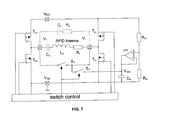
According to another specific aspect of the instant disclosure, a small capacitor Cp is added (with an optional resistor (Rp) connected in series) in parallel to the resonator circuit between power receiving terminals (shown, for example, in FIG. 7 ). During the small break-before-make gap the capacitor (Cp) conducts the antenna current and thereby avoids the excessive voltage generated by the antenna coil. The series resistor (Rp), if present, limits the current which charges the parallel capacitor (Cp) when the driver is activated again.
Based upon the above discussion and illustrations, those skilled in the art will readily recognize that various modifications and changes may be made without strictly following the exemplary embodiments and applications illustrated and described herein. Furthermore, various features of the different embodiments may be implemented in various combinations. Such modifications do not depart from the true spirit and scope of the present disclosure, including those set forth in the following claims.
Claims (15)
1. A transmission circuit comprising:
a resonance circuit, located between power-receiving terminals, wirelessly transmitting an information signal to an external circuit;
a capacitor and a resistor connected together in series between the power-receiving terminals; and
switching circuitry configured and arranged for:
generating different levels of square wave voltage signals by controlling coupling of the resonance circuit to power supply terminals, the different levels of square wave voltage signals including upper-level voltage signals, lower-level voltage signals, and mid-level voltage signals, to provide energy to the resonance circuit and, in turn, causing wireless transmission of the information signal; and when generating the mid-level voltage signals:
eliminating DC current paths between power-receiving terminals and the power supply terminals,
shorting the power-receiving terminals together thereby directing movement of charge stored in the resonance circuit from one of the power receiving terminals to the other power receiving terminal to generate the mid-level voltage signal, and
pausing during switching to create a break-before-make gap, wherein the capacitor and resistor are in a current path which is connected in parallel with the resonance circuit and which conducts current during the break-before-make gap.
2. The transmission circuit of claim 1 , wherein the switching circuitry further includes a feedback loop circuit configured and arranged to stabilize a mid-point potential of the circuit.
3. The transmission circuit of claim 1 , wherein the switching circuitry includes at least one switch.
4. The transmission circuit of claim 1 , wherein the resonance circuit has an operating frequency between 50 KHz and 150 KHz.
5. The transmission circuit of claim 1 , wherein the DC current paths are eliminated prior to shorting the power-receiving terminals together.
6. The transmission circuit of claim 1 , further including a proportional-integral-derivative controller (PID controller) circuit configured and arranged to control the switching circuitry.
7. The transmission circuit of claim 1 , further including a mixed-signals control circuit configured and arranged to control the switching circuitry.
8. The transmission circuit of claim 1 , wherein the shorting the power-receiving terminals together discharges an inductor of the resonance circuit.
9. The transmission circuit of claim 8 , wherein in generating the different levels of square wave voltage signals by the switching circuit provides a DC current path from one of the power supply terminals to the inductor of the resonance circuit.
10. A system comprising:
a transmission circuit, configured and arranged for transmitting an information signal, the transmission circuit including:
a transmission resonance circuit including a capacitor and a resistor located between power-receiving terminals, configured and arranged to wirelessly transmit the information signal,
switching circuitry configured and arranged for:
generating three different levels of square wave voltage signals by controlling coupling of the power-receiving terminals to power supply terminals, the three different levels of square wave voltage signals including upper-level, lower-level, and mid-level voltage signals, to provide energy to the transmission resonance circuit and, in turn, causing wireless transmission of the information signal, and when generating the mid-level voltage signals:
eliminating DC current paths from each of the power-receiving terminals to the power supply terminals, and
shorting the power-receiving terminals together and thereby directing movement of charge stored in the resonance circuit from one of the power receiving terminals to the other power receiving terminal to generate the mid-level voltage signals; and
pausing during switching to create a break-before-make gap, wherein the capacitor and resistor are in a current path which is connected in parallel with the resonance circuit and which conducts current during the break-before-make gap
a receiver circuit, configured and arranged to receive the information signal, the receiver circuit including:
a receiver resonance circuit configured and arranged to wirelessly receive the information signal, and
an identification circuit configured and arranged to confirm an authenticity of the transmission circuit.
11. The system of claim 10 , wherein the transmission circuit and the receiver resonance circuit are incorporated into an audio amplifier.
12. The system of claim 10 , wherein the transmission circuit and the receiver resonance circuit are incorporated into a passive-keyless entry device.
13. The system of claim 11 , wherein the transmission circuit and the receiver resonance circuit are incorporated into a contactless charging system.
14. The system of claim 10 , wherein the receiver resonator circuitry has an operating frequency between 50 and 150 KHz.
15. The system of claim 10 , wherein common mode attenuations of 40 dB or greater are achieved.
Priority Applications (5)
| Application Number | Priority Date | Filing Date | Title |
|---|---|---|---|
| US13/299,915 US9564948B2 (en) | 2011-11-18 | 2011-11-18 | 3-level bridge driver with single supply and low common mode EMI emission |
| EP12181694.6A EP2595318A3 (en) | 2011-11-18 | 2012-08-24 | 3-level bridge driver with single supply and low common mode EMI emission |
| JP2012243696A JP5564547B2 (en) | 2011-11-18 | 2012-11-05 | Low power common mode EMI radiation and single power supply 3-level bridge driver |
| CN201210458388.0A CN103124187B (en) | 2011-11-18 | 2012-11-14 | There are single supply and 3 grades of bridge drivers of low common mode EMI transmitting |
| KR1020120130572A KR101468277B1 (en) | 2011-11-18 | 2012-11-16 | 3-level bridge driver with single supply and low common mode emi emission |
Applications Claiming Priority (1)
| Application Number | Priority Date | Filing Date | Title |
|---|---|---|---|
| US13/299,915 US9564948B2 (en) | 2011-11-18 | 2011-11-18 | 3-level bridge driver with single supply and low common mode EMI emission |
Publications (2)
| Publication Number | Publication Date |
|---|---|
| US20130129016A1 US20130129016A1 (en) | 2013-05-23 |
| US9564948B2 true US9564948B2 (en) | 2017-02-07 |
Family
ID=47215351
Family Applications (1)
| Application Number | Title | Priority Date | Filing Date |
|---|---|---|---|
| US13/299,915 Active 2035-01-28 US9564948B2 (en) | 2011-11-18 | 2011-11-18 | 3-level bridge driver with single supply and low common mode EMI emission |
Country Status (5)
| Country | Link |
|---|---|
| US (1) | US9564948B2 (en) |
| EP (1) | EP2595318A3 (en) |
| JP (1) | JP5564547B2 (en) |
| KR (1) | KR101468277B1 (en) |
| CN (1) | CN103124187B (en) |
Cited By (3)
| Publication number | Priority date | Publication date | Assignee | Title |
|---|---|---|---|---|
| US9966837B1 (en) | 2016-07-08 | 2018-05-08 | Vpt, Inc. | Power converter with circuits for providing gate driving |
| US11427159B2 (en) | 2017-12-13 | 2022-08-30 | Denso Corporation | Antenna driving apparatus and antenna driving method |
| US11784578B2 (en) | 2022-01-28 | 2023-10-10 | Nxp B.V. | Electronic circuit with electromagnetic interference detection and suppression and method therefor |
Families Citing this family (3)
| Publication number | Priority date | Publication date | Assignee | Title |
|---|---|---|---|---|
| US9306498B2 (en) | 2014-02-13 | 2016-04-05 | Nxp B.V. | Current driven floating driver circuit |
| FR3030089B1 (en) * | 2014-12-12 | 2018-01-05 | Stmicroelectronics (Rousset) Sas | ELECTRONIC DEVICE HAVING RADIO FREQUENCY FUNCTION |
| EP3672069B1 (en) * | 2018-12-21 | 2022-06-22 | Nxp B.V. | A power amplifier and method of operating a power amplifier |
Citations (30)
| Publication number | Priority date | Publication date | Assignee | Title |
|---|---|---|---|---|
| US5504485A (en) * | 1994-07-21 | 1996-04-02 | Amtech Corporation | System for preventing reading of undesired RF signals |
| US5982230A (en) | 1995-09-07 | 1999-11-09 | Motorola, Inc. | Amplifier circuit |
| JP2001134233A (en) | 1999-11-09 | 2001-05-18 | Matsushita Electric Ind Co Ltd | Driving circuit and display device |
| US20020153902A1 (en) * | 2001-01-23 | 2002-10-24 | Holger Thiel | Circuit arrangement |
| EP1538036A1 (en) * | 2003-12-04 | 2005-06-08 | Alps Electric Co., Ltd. | Passive keyless entry device |
| US20070063041A1 (en) | 2005-09-21 | 2007-03-22 | Kenichi Kamiyama | Information processing apparatus and loop antenna |
| JP2007124732A (en) | 2005-10-25 | 2007-05-17 | Mitsubishi Electric Corp | Power converter |
| US20070176679A1 (en) * | 2006-02-01 | 2007-08-02 | Atmel Germany Gmbh | Differential amplifier and radio system with a differential amplifier |
| US20080064345A1 (en) | 2006-09-12 | 2008-03-13 | Denso Corporation | Device and method of radio wave transmission |
| US20080079492A1 (en) * | 2006-09-29 | 2008-04-03 | Sanyo Electric Co., Ltd. | Differential amplifier |
| US20080124162A1 (en) | 2006-11-28 | 2008-05-29 | Koshiro Yamaguchi | RFID tag information communicating apparatus |
| US20080223931A1 (en) * | 2005-10-17 | 2008-09-18 | Nxp B.V. | Electronic Circuit for a Contactless Reader Device |
| KR20080093641A (en) | 2007-04-17 | 2008-10-22 | 전남대학교산학협력단 | Multi-level inverter using 3-phase transformers and common-arm |
| US20080261555A1 (en) * | 2007-04-18 | 2008-10-23 | Yung-Chin Chen | Intertalk wristband radio frequency identification tag |
| US7479884B1 (en) * | 2004-08-31 | 2009-01-20 | Cedar Ridge Research | System and method for monitoring objects, people, animals or places |
| US20090224893A1 (en) | 2005-04-15 | 2009-09-10 | Satoru Kondo | Communication device, non-contact type ic card mounting same, and information apparatus |
| US20090247079A1 (en) | 2008-03-31 | 2009-10-01 | Stmicroelectronics (Rousset) Sas | Terminal of radio-frequency transmission/reception by inductive coupling |
| US20090289716A1 (en) * | 2008-05-23 | 2009-11-26 | Freescale Semiconductor, Inc. | Amplifier circuit having dynamically biased configuration |
| US20100009627A1 (en) | 2006-12-15 | 2010-01-14 | Heikki Huomo | Nfc communicator and method of data communication |
| US20100073063A1 (en) | 2008-09-19 | 2010-03-25 | Ikanos Communications, Inc. | 3-Level Line Driver |
| US7772904B1 (en) * | 2009-02-16 | 2010-08-10 | Infineon Technologies Ag | Voltage level converter with mixed signal controller |
| US20100225391A1 (en) | 2009-03-03 | 2010-09-09 | Samsung Electronics Co., Ltd. | Three-level half-bridge pulse-width modulation amplifier and method of driving the same |
| US20110064245A1 (en) | 2009-09-16 | 2011-03-17 | Kim Bong-Joo | Half-bridge three-level pwm amplifier and audio processing apparatus including the same |
| US7928848B2 (en) | 2007-08-02 | 2011-04-19 | Brother Kogyo Kabushiki Kaisha | RFID tag producing apparatus |
| US20110102026A1 (en) | 2009-11-05 | 2011-05-05 | Rohm Co., Ltd. | Antenna driving device |
| US20110156640A1 (en) * | 2009-12-25 | 2011-06-30 | Mehran Moshfeghi | Method and apparatus for wirelessly transferring power and communicating with one or more slave devices |
| JP2012518337A (en) | 2009-02-13 | 2012-08-09 | クアルコム,インコーポレイテッド | Antenna sharing for wireless powered devices |
| US20120278192A1 (en) * | 2011-04-28 | 2012-11-01 | Etan Shirron | Device, system and method of wirelessly delivering content |
| US20120277018A1 (en) * | 2011-04-28 | 2012-11-01 | Nike, Inc. | Golf Clubs and Golf Club Heads |
| US20130223651A1 (en) * | 2010-10-27 | 2013-08-29 | Merus Audio Aps | Audio amplifier using multi-level pulse width modulation |
Family Cites Families (1)
| Publication number | Priority date | Publication date | Assignee | Title |
|---|---|---|---|---|
| US3594653A (en) * | 1969-12-31 | 1971-07-20 | Ibm | Cross-coupled differential amplifier |
-
2011
- 2011-11-18 US US13/299,915 patent/US9564948B2/en active Active
-
2012
- 2012-08-24 EP EP12181694.6A patent/EP2595318A3/en not_active Withdrawn
- 2012-11-05 JP JP2012243696A patent/JP5564547B2/en active Active
- 2012-11-14 CN CN201210458388.0A patent/CN103124187B/en active Active
- 2012-11-16 KR KR1020120130572A patent/KR101468277B1/en active IP Right Grant
Patent Citations (36)
| Publication number | Priority date | Publication date | Assignee | Title |
|---|---|---|---|---|
| US5504485A (en) * | 1994-07-21 | 1996-04-02 | Amtech Corporation | System for preventing reading of undesired RF signals |
| US5982230A (en) | 1995-09-07 | 1999-11-09 | Motorola, Inc. | Amplifier circuit |
| JP2000513510A (en) | 1995-09-07 | 2000-10-10 | モトローラ・インコーポレーテッド | Amplifier circuit |
| JP2001134233A (en) | 1999-11-09 | 2001-05-18 | Matsushita Electric Ind Co Ltd | Driving circuit and display device |
| US20020153902A1 (en) * | 2001-01-23 | 2002-10-24 | Holger Thiel | Circuit arrangement |
| EP1538036A1 (en) * | 2003-12-04 | 2005-06-08 | Alps Electric Co., Ltd. | Passive keyless entry device |
| JP2005163453A (en) * | 2003-12-04 | 2005-06-23 | Alps Electric Co Ltd | Passive keyless entry device |
| US7479884B1 (en) * | 2004-08-31 | 2009-01-20 | Cedar Ridge Research | System and method for monitoring objects, people, animals or places |
| US20090224893A1 (en) | 2005-04-15 | 2009-09-10 | Satoru Kondo | Communication device, non-contact type ic card mounting same, and information apparatus |
| US20070063041A1 (en) | 2005-09-21 | 2007-03-22 | Kenichi Kamiyama | Information processing apparatus and loop antenna |
| US20080223931A1 (en) * | 2005-10-17 | 2008-09-18 | Nxp B.V. | Electronic Circuit for a Contactless Reader Device |
| JP2007124732A (en) | 2005-10-25 | 2007-05-17 | Mitsubishi Electric Corp | Power converter |
| US20070176679A1 (en) * | 2006-02-01 | 2007-08-02 | Atmel Germany Gmbh | Differential amplifier and radio system with a differential amplifier |
| JP2008072210A (en) | 2006-09-12 | 2008-03-27 | Denso Corp | On-vehicle radio transmitter |
| US20080064345A1 (en) | 2006-09-12 | 2008-03-13 | Denso Corporation | Device and method of radio wave transmission |
| US20080079492A1 (en) * | 2006-09-29 | 2008-04-03 | Sanyo Electric Co., Ltd. | Differential amplifier |
| US20080124162A1 (en) | 2006-11-28 | 2008-05-29 | Koshiro Yamaguchi | RFID tag information communicating apparatus |
| US20100009627A1 (en) | 2006-12-15 | 2010-01-14 | Heikki Huomo | Nfc communicator and method of data communication |
| KR20080093641A (en) | 2007-04-17 | 2008-10-22 | 전남대학교산학협력단 | Multi-level inverter using 3-phase transformers and common-arm |
| US20080261555A1 (en) * | 2007-04-18 | 2008-10-23 | Yung-Chin Chen | Intertalk wristband radio frequency identification tag |
| US7928848B2 (en) | 2007-08-02 | 2011-04-19 | Brother Kogyo Kabushiki Kaisha | RFID tag producing apparatus |
| US20090247079A1 (en) | 2008-03-31 | 2009-10-01 | Stmicroelectronics (Rousset) Sas | Terminal of radio-frequency transmission/reception by inductive coupling |
| US20090289716A1 (en) * | 2008-05-23 | 2009-11-26 | Freescale Semiconductor, Inc. | Amplifier circuit having dynamically biased configuration |
| US20100073063A1 (en) | 2008-09-19 | 2010-03-25 | Ikanos Communications, Inc. | 3-Level Line Driver |
| JP2012518337A (en) | 2009-02-13 | 2012-08-09 | クアルコム,インコーポレイテッド | Antenna sharing for wireless powered devices |
| US20140152253A1 (en) | 2009-02-13 | 2014-06-05 | Qualcomm Incorporated | Antenna sharing for wirelessly powered devices |
| US7772904B1 (en) * | 2009-02-16 | 2010-08-10 | Infineon Technologies Ag | Voltage level converter with mixed signal controller |
| US20100225391A1 (en) | 2009-03-03 | 2010-09-09 | Samsung Electronics Co., Ltd. | Three-level half-bridge pulse-width modulation amplifier and method of driving the same |
| KR20100099544A (en) | 2009-03-03 | 2010-09-13 | 삼성전자주식회사 | Half-bridge 3-level pulse-width modulation amplifier, audio apparatus and driving method of the pwm amplifier |
| KR20110029776A (en) | 2009-09-16 | 2011-03-23 | 삼성전자주식회사 | Half-bridge 3-level pwm amplifier, method of driving the same and audio processing apparatus |
| US20110064245A1 (en) | 2009-09-16 | 2011-03-17 | Kim Bong-Joo | Half-bridge three-level pwm amplifier and audio processing apparatus including the same |
| US20110102026A1 (en) | 2009-11-05 | 2011-05-05 | Rohm Co., Ltd. | Antenna driving device |
| US20110156640A1 (en) * | 2009-12-25 | 2011-06-30 | Mehran Moshfeghi | Method and apparatus for wirelessly transferring power and communicating with one or more slave devices |
| US20130223651A1 (en) * | 2010-10-27 | 2013-08-29 | Merus Audio Aps | Audio amplifier using multi-level pulse width modulation |
| US20120278192A1 (en) * | 2011-04-28 | 2012-11-01 | Etan Shirron | Device, system and method of wirelessly delivering content |
| US20120277018A1 (en) * | 2011-04-28 | 2012-11-01 | Nike, Inc. | Golf Clubs and Golf Club Heads |
Non-Patent Citations (3)
| Title |
|---|
| Extended European Search Report for European Patent Appln. No. 12181694.6 (Jul. 4, 2014). |
| Japanese Patent Application No. 2012-243696, Notice of Grant, May 21, 2014. |
| Korean Patent Appln. No. 1012-0130572, Notice Of Allowance, Nov. 12, 2014. |
Cited By (3)
| Publication number | Priority date | Publication date | Assignee | Title |
|---|---|---|---|---|
| US9966837B1 (en) | 2016-07-08 | 2018-05-08 | Vpt, Inc. | Power converter with circuits for providing gate driving |
| US11427159B2 (en) | 2017-12-13 | 2022-08-30 | Denso Corporation | Antenna driving apparatus and antenna driving method |
| US11784578B2 (en) | 2022-01-28 | 2023-10-10 | Nxp B.V. | Electronic circuit with electromagnetic interference detection and suppression and method therefor |
Also Published As
| Publication number | Publication date |
|---|---|
| US20130129016A1 (en) | 2013-05-23 |
| EP2595318A2 (en) | 2013-05-22 |
| JP2013128270A (en) | 2013-06-27 |
| CN103124187A (en) | 2013-05-29 |
| EP2595318A3 (en) | 2014-08-06 |
| KR101468277B1 (en) | 2014-12-03 |
| KR20130055546A (en) | 2013-05-28 |
| CN103124187B (en) | 2016-09-28 |
| JP5564547B2 (en) | 2014-07-30 |
Similar Documents
| Publication | Publication Date | Title |
|---|---|---|
| US9564948B2 (en) | 3-level bridge driver with single supply and low common mode EMI emission | |
| CN105429625B (en) | Method and structure for generating on/off keying carrier signal for signal isolator | |
| US10277208B2 (en) | Energy efficient controlled magnetic field generator circuit | |
| EP3402070B1 (en) | Class d audio amplifier with adjustable gate drive | |
| US9893534B2 (en) | Relay device of wireless power transmission system | |
| CN110785911A (en) | System, apparatus and method for adaptive tuning of wireless power transmission | |
| WO2013132755A1 (en) | Wireless receiver, wireless power supply, and wireless transmission system | |
| JP6336120B2 (en) | Inductor driver circuit and active transmission device having driver circuit | |
| US20140183972A1 (en) | Wireless power transmitter and wireless power receiver | |
| US10389314B2 (en) | High-voltage digital power amplifier with sinusoidal output for RFID | |
| JP6452813B2 (en) | Inductor driver circuit | |
| EP2108218A1 (en) | Sampling frequency reduction for switching amplifiers | |
| CN105580275A (en) | Driver circuit for an inductor coil, method for operating an inductor coil, and active transmission system having a driver circuit | |
| US11218347B2 (en) | ASK modulation | |
| EP3139497B1 (en) | Oscillator with favorable startup | |
| US10879739B2 (en) | Wireless power transmitter reactive energy control | |
| US10579916B2 (en) | Low power magnetic secure transmission system | |
| JP3875100B2 (en) | Output stage using floating power supply | |
| US20170353157A1 (en) | Methods and apparatus for generating a high swing in an oscillator | |
| US11303154B2 (en) | Half-half-bridge pulse width modulation low power magnetic secure transmission systems | |
| US8482350B2 (en) | Low RF interference switching amplifier and method | |
| EP2963822B1 (en) | Protection switching for matrix of ferrite modules with redundant control | |
| JP2013106490A (en) | Wireless power-feeding device, wireless power-feeding system, and transmission method of power signal | |
| EP3573232B1 (en) | Common mode voltage ramping in class-d amplifiers minimizing am band emissions in passive keyless entry systems | |
| US20230238964A1 (en) | Transmission circuit |
Legal Events
| Date | Code | Title | Description |
|---|---|---|---|
| AS | Assignment |
Owner name: NXP B.V., NETHERLANDS Free format text: ASSIGNMENT OF ASSIGNORS INTEREST;ASSIGNORS:ARNOLD, SIEGFRIED;KOFLER, ROBERT;MASCHERA, DAVIDE;AND OTHERS;REEL/FRAME:027272/0443 Effective date: 20111118 |
|
| STCF | Information on status: patent grant |
Free format text: PATENTED CASE |
|
| MAFP | Maintenance fee payment |
Free format text: PAYMENT OF MAINTENANCE FEE, 4TH YEAR, LARGE ENTITY (ORIGINAL EVENT CODE: M1551); ENTITY STATUS OF PATENT OWNER: LARGE ENTITY Year of fee payment: 4 |