US9537010B2 - Semiconductor device structure and method for forming the same - Google Patents
Semiconductor device structure and method for forming the same Download PDFInfo
- Publication number
- US9537010B2 US9537010B2 US14/613,663 US201514613663A US9537010B2 US 9537010 B2 US9537010 B2 US 9537010B2 US 201514613663 A US201514613663 A US 201514613663A US 9537010 B2 US9537010 B2 US 9537010B2
- Authority
- US
- United States
- Prior art keywords
- accordance
- substrate
- layer
- semiconductor device
- over
- Prior art date
- Legal status (The legal status is an assumption and is not a legal conclusion. Google has not performed a legal analysis and makes no representation as to the accuracy of the status listed.)
- Active
Links
- 239000004065 semiconductor Substances 0.000 title claims abstract description 89
- 238000000034 method Methods 0.000 title claims description 212
- 239000002019 doping agent Substances 0.000 claims abstract description 107
- 239000000758 substrate Substances 0.000 claims abstract description 101
- 238000002955 isolation Methods 0.000 claims abstract description 46
- 238000009792 diffusion process Methods 0.000 claims description 59
- 239000000463 material Substances 0.000 claims description 51
- 238000002513 implantation Methods 0.000 claims description 49
- 238000000137 annealing Methods 0.000 claims description 18
- 150000004767 nitrides Chemical class 0.000 claims description 6
- 230000015572 biosynthetic process Effects 0.000 claims description 5
- 239000010410 layer Substances 0.000 description 279
- 238000000206 photolithography Methods 0.000 description 25
- 229910052751 metal Inorganic materials 0.000 description 18
- 239000002184 metal Substances 0.000 description 18
- 239000003989 dielectric material Substances 0.000 description 15
- 238000005229 chemical vapour deposition Methods 0.000 description 14
- 229910015900 BF3 Inorganic materials 0.000 description 12
- WTEOIRVLGSZEPR-UHFFFAOYSA-N boron trifluoride Chemical compound FB(F)F WTEOIRVLGSZEPR-UHFFFAOYSA-N 0.000 description 12
- 238000001039 wet etching Methods 0.000 description 11
- 238000001312 dry etching Methods 0.000 description 10
- VYPSYNLAJGMNEJ-UHFFFAOYSA-N Silicium dioxide Chemical compound O=[Si]=O VYPSYNLAJGMNEJ-UHFFFAOYSA-N 0.000 description 9
- 238000000576 coating method Methods 0.000 description 9
- 238000005137 deposition process Methods 0.000 description 9
- 238000005530 etching Methods 0.000 description 9
- 238000005468 ion implantation Methods 0.000 description 9
- 229920002120 photoresistant polymer Polymers 0.000 description 9
- 229910052814 silicon oxide Inorganic materials 0.000 description 9
- 125000006850 spacer group Chemical group 0.000 description 9
- ZOXJGFHDIHLPTG-UHFFFAOYSA-N Boron Chemical compound [B] ZOXJGFHDIHLPTG-UHFFFAOYSA-N 0.000 description 6
- XUIMIQQOPSSXEZ-UHFFFAOYSA-N Silicon Chemical compound [Si] XUIMIQQOPSSXEZ-UHFFFAOYSA-N 0.000 description 6
- 238000000231 atomic layer deposition Methods 0.000 description 6
- 229910052796 boron Inorganic materials 0.000 description 6
- 229910052710 silicon Inorganic materials 0.000 description 6
- 239000010703 silicon Substances 0.000 description 6
- OAICVXFJPJFONN-UHFFFAOYSA-N Phosphorus Chemical compound [P] OAICVXFJPJFONN-UHFFFAOYSA-N 0.000 description 5
- 229910052785 arsenic Inorganic materials 0.000 description 5
- RQNWIZPPADIBDY-UHFFFAOYSA-N arsenic atom Chemical compound [As] RQNWIZPPADIBDY-UHFFFAOYSA-N 0.000 description 5
- 229910052698 phosphorus Inorganic materials 0.000 description 5
- 239000011574 phosphorus Substances 0.000 description 5
- 229910052581 Si3N4 Inorganic materials 0.000 description 4
- 229910045601 alloy Inorganic materials 0.000 description 4
- 239000000956 alloy Substances 0.000 description 4
- 239000005388 borosilicate glass Substances 0.000 description 4
- 230000005669 field effect Effects 0.000 description 4
- 238000004519 manufacturing process Methods 0.000 description 4
- 230000000149 penetrating effect Effects 0.000 description 4
- 238000005240 physical vapour deposition Methods 0.000 description 4
- BASFCYQUMIYNBI-UHFFFAOYSA-N platinum Chemical compound [Pt] BASFCYQUMIYNBI-UHFFFAOYSA-N 0.000 description 4
- HQVNEWCFYHHQES-UHFFFAOYSA-N silicon nitride Chemical compound N12[Si]34N5[Si]62N3[Si]51N64 HQVNEWCFYHHQES-UHFFFAOYSA-N 0.000 description 4
- 239000002194 amorphous carbon material Substances 0.000 description 3
- 239000012212 insulator Substances 0.000 description 3
- 238000007747 plating Methods 0.000 description 3
- 238000005498 polishing Methods 0.000 description 3
- 229910021420 polycrystalline silicon Inorganic materials 0.000 description 3
- 229920005591 polysilicon Polymers 0.000 description 3
- 239000005368 silicate glass Substances 0.000 description 3
- 239000000126 substance Substances 0.000 description 3
- 229910000577 Silicon-germanium Inorganic materials 0.000 description 2
- 229910052782 aluminium Inorganic materials 0.000 description 2
- XAGFODPZIPBFFR-UHFFFAOYSA-N aluminium Chemical compound [Al] XAGFODPZIPBFFR-UHFFFAOYSA-N 0.000 description 2
- PNEYBMLMFCGWSK-UHFFFAOYSA-N aluminium oxide Inorganic materials [O-2].[O-2].[O-2].[Al+3].[Al+3] PNEYBMLMFCGWSK-UHFFFAOYSA-N 0.000 description 2
- 239000005380 borophosphosilicate glass Substances 0.000 description 2
- 229910017052 cobalt Inorganic materials 0.000 description 2
- 239000010941 cobalt Substances 0.000 description 2
- GUTLYIVDDKVIGB-UHFFFAOYSA-N cobalt atom Chemical compound [Co] GUTLYIVDDKVIGB-UHFFFAOYSA-N 0.000 description 2
- 230000009969 flowable effect Effects 0.000 description 2
- 229910052732 germanium Inorganic materials 0.000 description 2
- GNPVGFCGXDBREM-UHFFFAOYSA-N germanium atom Chemical compound [Ge] GNPVGFCGXDBREM-UHFFFAOYSA-N 0.000 description 2
- PCHJSUWPFVWCPO-UHFFFAOYSA-N gold Chemical compound [Au] PCHJSUWPFVWCPO-UHFFFAOYSA-N 0.000 description 2
- 229910052737 gold Inorganic materials 0.000 description 2
- 239000010931 gold Substances 0.000 description 2
- 229910052735 hafnium Inorganic materials 0.000 description 2
- VBJZVLUMGGDVMO-UHFFFAOYSA-N hafnium atom Chemical compound [Hf] VBJZVLUMGGDVMO-UHFFFAOYSA-N 0.000 description 2
- 239000007769 metal material Substances 0.000 description 2
- 238000000059 patterning Methods 0.000 description 2
- 229910052697 platinum Inorganic materials 0.000 description 2
- HBMJWWWQQXIZIP-UHFFFAOYSA-N silicon carbide Chemical compound [Si+]#[C-] HBMJWWWQQXIZIP-UHFFFAOYSA-N 0.000 description 2
- 229910010271 silicon carbide Inorganic materials 0.000 description 2
- -1 silicon nitride Chemical class 0.000 description 2
- 239000007790 solid phase Substances 0.000 description 2
- 238000004544 sputter deposition Methods 0.000 description 2
- WFKWXMTUELFFGS-UHFFFAOYSA-N tungsten Chemical compound [W] WFKWXMTUELFFGS-UHFFFAOYSA-N 0.000 description 2
- 229910052721 tungsten Inorganic materials 0.000 description 2
- 239000010937 tungsten Substances 0.000 description 2
- JBRZTFJDHDCESZ-UHFFFAOYSA-N AsGa Chemical compound [As]#[Ga] JBRZTFJDHDCESZ-UHFFFAOYSA-N 0.000 description 1
- 229910005540 GaP Inorganic materials 0.000 description 1
- 229910001218 Gallium arsenide Inorganic materials 0.000 description 1
- 229910000673 Indium arsenide Inorganic materials 0.000 description 1
- GPXJNWSHGFTCBW-UHFFFAOYSA-N Indium phosphide Chemical compound [In]#P GPXJNWSHGFTCBW-UHFFFAOYSA-N 0.000 description 1
- BPQQTUXANYXVAA-UHFFFAOYSA-N Orthosilicate Chemical compound [O-][Si]([O-])([O-])[O-] BPQQTUXANYXVAA-UHFFFAOYSA-N 0.000 description 1
- RTAQQCXQSZGOHL-UHFFFAOYSA-N Titanium Chemical compound [Ti] RTAQQCXQSZGOHL-UHFFFAOYSA-N 0.000 description 1
- NRTOMJZYCJJWKI-UHFFFAOYSA-N Titanium nitride Chemical compound [Ti]#N NRTOMJZYCJJWKI-UHFFFAOYSA-N 0.000 description 1
- CEPICIBPGDWCRU-UHFFFAOYSA-N [Si].[Hf] Chemical compound [Si].[Hf] CEPICIBPGDWCRU-UHFFFAOYSA-N 0.000 description 1
- ILCYGSITMBHYNK-UHFFFAOYSA-N [Si]=O.[Hf] Chemical compound [Si]=O.[Hf] ILCYGSITMBHYNK-UHFFFAOYSA-N 0.000 description 1
- 230000004075 alteration Effects 0.000 description 1
- 238000004140 cleaning Methods 0.000 description 1
- 150000001875 compounds Chemical class 0.000 description 1
- 238000010276 construction Methods 0.000 description 1
- 229910052593 corundum Inorganic materials 0.000 description 1
- 239000013078 crystal Substances 0.000 description 1
- 230000003247 decreasing effect Effects 0.000 description 1
- HZXMRANICFIONG-UHFFFAOYSA-N gallium phosphide Chemical compound [Ga]#P HZXMRANICFIONG-UHFFFAOYSA-N 0.000 description 1
- ZQXQADNTSSMHJI-UHFFFAOYSA-N hafnium(4+) oxygen(2-) tantalum(5+) Chemical compound [O-2].[Ta+5].[Hf+4] ZQXQADNTSSMHJI-UHFFFAOYSA-N 0.000 description 1
- KQHQLIAOAVMAOW-UHFFFAOYSA-N hafnium(4+) oxygen(2-) zirconium(4+) Chemical compound [O--].[O--].[O--].[O--].[Zr+4].[Hf+4] KQHQLIAOAVMAOW-UHFFFAOYSA-N 0.000 description 1
- KUVFGOLWQIXGBP-UHFFFAOYSA-N hafnium(4+);oxygen(2-);titanium(4+) Chemical compound [O-2].[O-2].[O-2].[O-2].[Ti+4].[Hf+4] KUVFGOLWQIXGBP-UHFFFAOYSA-N 0.000 description 1
- CJNBYAVZURUTKZ-UHFFFAOYSA-N hafnium(iv) oxide Chemical compound O=[Hf]=O CJNBYAVZURUTKZ-UHFFFAOYSA-N 0.000 description 1
- RPQDHPTXJYYUPQ-UHFFFAOYSA-N indium arsenide Chemical compound [In]#[As] RPQDHPTXJYYUPQ-UHFFFAOYSA-N 0.000 description 1
- 239000011810 insulating material Substances 0.000 description 1
- 239000011229 interlayer Substances 0.000 description 1
- 229910044991 metal oxide Inorganic materials 0.000 description 1
- 150000004706 metal oxides Chemical class 0.000 description 1
- 229910052914 metal silicate Inorganic materials 0.000 description 1
- 150000002739 metals Chemical class 0.000 description 1
- 229910003465 moissanite Inorganic materials 0.000 description 1
- 230000003647 oxidation Effects 0.000 description 1
- 238000007254 oxidation reaction Methods 0.000 description 1
- TWNQGVIAIRXVLR-UHFFFAOYSA-N oxo(oxoalumanyloxy)alumane Chemical compound O=[Al]O[Al]=O TWNQGVIAIRXVLR-UHFFFAOYSA-N 0.000 description 1
- OYLRFHLPEAGKJU-UHFFFAOYSA-N phosphane silicic acid Chemical compound P.[Si](O)(O)(O)O OYLRFHLPEAGKJU-UHFFFAOYSA-N 0.000 description 1
- 150000004760 silicates Chemical class 0.000 description 1
- 238000006467 substitution reaction Methods 0.000 description 1
- 229910052715 tantalum Inorganic materials 0.000 description 1
- GUVRBAGPIYLISA-UHFFFAOYSA-N tantalum atom Chemical compound [Ta] GUVRBAGPIYLISA-UHFFFAOYSA-N 0.000 description 1
- MZLGASXMSKOWSE-UHFFFAOYSA-N tantalum nitride Chemical compound [Ta]#N MZLGASXMSKOWSE-UHFFFAOYSA-N 0.000 description 1
- 239000010936 titanium Substances 0.000 description 1
- 229910052719 titanium Inorganic materials 0.000 description 1
- 230000007704 transition Effects 0.000 description 1
- 229910000314 transition metal oxide Inorganic materials 0.000 description 1
- 229910000326 transition metal silicate Inorganic materials 0.000 description 1
- 229910001845 yogo sapphire Inorganic materials 0.000 description 1
Images


Classifications
-
- H—ELECTRICITY
- H01—ELECTRIC ELEMENTS
- H01L—SEMICONDUCTOR DEVICES NOT COVERED BY CLASS H10
- H01L29/00—Semiconductor devices specially adapted for rectifying, amplifying, oscillating or switching and having potential barriers; Capacitors or resistors having potential barriers, e.g. a PN-junction depletion layer or carrier concentration layer; Details of semiconductor bodies or of electrodes thereof ; Multistep manufacturing processes therefor
- H01L29/66—Types of semiconductor device ; Multistep manufacturing processes therefor
- H01L29/68—Types of semiconductor device ; Multistep manufacturing processes therefor controllable by only the electric current supplied, or only the electric potential applied, to an electrode which does not carry the current to be rectified, amplified or switched
- H01L29/76—Unipolar devices, e.g. field effect transistors
- H01L29/772—Field effect transistors
- H01L29/78—Field effect transistors with field effect produced by an insulated gate
- H01L29/785—Field effect transistors with field effect produced by an insulated gate having a channel with a horizontal current flow in a vertical sidewall of a semiconductor body, e.g. FinFET, MuGFET
- H01L29/7856—Field effect transistors with field effect produced by an insulated gate having a channel with a horizontal current flow in a vertical sidewall of a semiconductor body, e.g. FinFET, MuGFET with an non-uniform gate, e.g. varying doping structure, shape or composition on different sides of the fin, or different gate insulator thickness or composition on opposing fin sides
-
- H—ELECTRICITY
- H01—ELECTRIC ELEMENTS
- H01L—SEMICONDUCTOR DEVICES NOT COVERED BY CLASS H10
- H01L29/00—Semiconductor devices specially adapted for rectifying, amplifying, oscillating or switching and having potential barriers; Capacitors or resistors having potential barriers, e.g. a PN-junction depletion layer or carrier concentration layer; Details of semiconductor bodies or of electrodes thereof ; Multistep manufacturing processes therefor
- H01L29/66—Types of semiconductor device ; Multistep manufacturing processes therefor
- H01L29/66007—Multistep manufacturing processes
- H01L29/66075—Multistep manufacturing processes of devices having semiconductor bodies comprising group 14 or group 13/15 materials
- H01L29/66227—Multistep manufacturing processes of devices having semiconductor bodies comprising group 14 or group 13/15 materials the devices being controllable only by the electric current supplied or the electric potential applied, to an electrode which does not carry the current to be rectified, amplified or switched, e.g. three-terminal devices
- H01L29/66409—Unipolar field-effect transistors
- H01L29/66477—Unipolar field-effect transistors with an insulated gate, i.e. MISFET
- H01L29/66787—Unipolar field-effect transistors with an insulated gate, i.e. MISFET with a gate at the side of the channel
- H01L29/66795—Unipolar field-effect transistors with an insulated gate, i.e. MISFET with a gate at the side of the channel with a horizontal current flow in a vertical sidewall of a semiconductor body, e.g. FinFET, MuGFET
-
- H—ELECTRICITY
- H01—ELECTRIC ELEMENTS
- H01L—SEMICONDUCTOR DEVICES NOT COVERED BY CLASS H10
- H01L21/00—Processes or apparatus adapted for the manufacture or treatment of semiconductor or solid state devices or of parts thereof
- H01L21/02—Manufacture or treatment of semiconductor devices or of parts thereof
- H01L21/04—Manufacture or treatment of semiconductor devices or of parts thereof the devices having potential barriers, e.g. a PN junction, depletion layer or carrier concentration layer
- H01L21/18—Manufacture or treatment of semiconductor devices or of parts thereof the devices having potential barriers, e.g. a PN junction, depletion layer or carrier concentration layer the devices having semiconductor bodies comprising elements of Group IV of the Periodic Table or AIIIBV compounds with or without impurities, e.g. doping materials
- H01L21/22—Diffusion of impurity materials, e.g. doping materials, electrode materials, into or out of a semiconductor body, or between semiconductor regions; Interactions between two or more impurities; Redistribution of impurities
- H01L21/225—Diffusion of impurity materials, e.g. doping materials, electrode materials, into or out of a semiconductor body, or between semiconductor regions; Interactions between two or more impurities; Redistribution of impurities using diffusion into or out of a solid from or into a solid phase, e.g. a doped oxide layer
- H01L21/2251—Diffusion into or out of group IV semiconductors
- H01L21/2252—Diffusion into or out of group IV semiconductors using predeposition of impurities into the semiconductor surface, e.g. from a gaseous phase
- H01L21/2253—Diffusion into or out of group IV semiconductors using predeposition of impurities into the semiconductor surface, e.g. from a gaseous phase by ion implantation
-
- H—ELECTRICITY
- H01—ELECTRIC ELEMENTS
- H01L—SEMICONDUCTOR DEVICES NOT COVERED BY CLASS H10
- H01L21/00—Processes or apparatus adapted for the manufacture or treatment of semiconductor or solid state devices or of parts thereof
- H01L21/02—Manufacture or treatment of semiconductor devices or of parts thereof
- H01L21/04—Manufacture or treatment of semiconductor devices or of parts thereof the devices having potential barriers, e.g. a PN junction, depletion layer or carrier concentration layer
- H01L21/18—Manufacture or treatment of semiconductor devices or of parts thereof the devices having potential barriers, e.g. a PN junction, depletion layer or carrier concentration layer the devices having semiconductor bodies comprising elements of Group IV of the Periodic Table or AIIIBV compounds with or without impurities, e.g. doping materials
- H01L21/26—Bombardment with radiation
- H01L21/263—Bombardment with radiation with high-energy radiation
- H01L21/265—Bombardment with radiation with high-energy radiation producing ion implantation
- H01L21/266—Bombardment with radiation with high-energy radiation producing ion implantation using masks
-
- H—ELECTRICITY
- H01—ELECTRIC ELEMENTS
- H01L—SEMICONDUCTOR DEVICES NOT COVERED BY CLASS H10
- H01L21/00—Processes or apparatus adapted for the manufacture or treatment of semiconductor or solid state devices or of parts thereof
- H01L21/02—Manufacture or treatment of semiconductor devices or of parts thereof
- H01L21/04—Manufacture or treatment of semiconductor devices or of parts thereof the devices having potential barriers, e.g. a PN junction, depletion layer or carrier concentration layer
- H01L21/18—Manufacture or treatment of semiconductor devices or of parts thereof the devices having potential barriers, e.g. a PN junction, depletion layer or carrier concentration layer the devices having semiconductor bodies comprising elements of Group IV of the Periodic Table or AIIIBV compounds with or without impurities, e.g. doping materials
- H01L21/30—Treatment of semiconductor bodies using processes or apparatus not provided for in groups H01L21/20 - H01L21/26
- H01L21/324—Thermal treatment for modifying the properties of semiconductor bodies, e.g. annealing, sintering
-
- H—ELECTRICITY
- H01—ELECTRIC ELEMENTS
- H01L—SEMICONDUCTOR DEVICES NOT COVERED BY CLASS H10
- H01L21/00—Processes or apparatus adapted for the manufacture or treatment of semiconductor or solid state devices or of parts thereof
- H01L21/70—Manufacture or treatment of devices consisting of a plurality of solid state components formed in or on a common substrate or of parts thereof; Manufacture of integrated circuit devices or of parts thereof
- H01L21/77—Manufacture or treatment of devices consisting of a plurality of solid state components or integrated circuits formed in, or on, a common substrate
- H01L21/78—Manufacture or treatment of devices consisting of a plurality of solid state components or integrated circuits formed in, or on, a common substrate with subsequent division of the substrate into plural individual devices
- H01L21/82—Manufacture or treatment of devices consisting of a plurality of solid state components or integrated circuits formed in, or on, a common substrate with subsequent division of the substrate into plural individual devices to produce devices, e.g. integrated circuits, each consisting of a plurality of components
- H01L21/822—Manufacture or treatment of devices consisting of a plurality of solid state components or integrated circuits formed in, or on, a common substrate with subsequent division of the substrate into plural individual devices to produce devices, e.g. integrated circuits, each consisting of a plurality of components the substrate being a semiconductor, using silicon technology
- H01L21/8232—Field-effect technology
- H01L21/8234—MIS technology, i.e. integration processes of field effect transistors of the conductor-insulator-semiconductor type
- H01L21/8238—Complementary field-effect transistors, e.g. CMOS
- H01L21/823821—Complementary field-effect transistors, e.g. CMOS with a particular manufacturing method of transistors with a horizontal current flow in a vertical sidewall of a semiconductor body, e.g. FinFET, MuGFET
-
- H—ELECTRICITY
- H01—ELECTRIC ELEMENTS
- H01L—SEMICONDUCTOR DEVICES NOT COVERED BY CLASS H10
- H01L27/00—Devices consisting of a plurality of semiconductor or other solid-state components formed in or on a common substrate
- H01L27/02—Devices consisting of a plurality of semiconductor or other solid-state components formed in or on a common substrate including semiconductor components specially adapted for rectifying, oscillating, amplifying or switching and having potential barriers; including integrated passive circuit elements having potential barriers
- H01L27/04—Devices consisting of a plurality of semiconductor or other solid-state components formed in or on a common substrate including semiconductor components specially adapted for rectifying, oscillating, amplifying or switching and having potential barriers; including integrated passive circuit elements having potential barriers the substrate being a semiconductor body
- H01L27/08—Devices consisting of a plurality of semiconductor or other solid-state components formed in or on a common substrate including semiconductor components specially adapted for rectifying, oscillating, amplifying or switching and having potential barriers; including integrated passive circuit elements having potential barriers the substrate being a semiconductor body including only semiconductor components of a single kind
- H01L27/085—Devices consisting of a plurality of semiconductor or other solid-state components formed in or on a common substrate including semiconductor components specially adapted for rectifying, oscillating, amplifying or switching and having potential barriers; including integrated passive circuit elements having potential barriers the substrate being a semiconductor body including only semiconductor components of a single kind including field-effect components only
- H01L27/088—Devices consisting of a plurality of semiconductor or other solid-state components formed in or on a common substrate including semiconductor components specially adapted for rectifying, oscillating, amplifying or switching and having potential barriers; including integrated passive circuit elements having potential barriers the substrate being a semiconductor body including only semiconductor components of a single kind including field-effect components only the components being field-effect transistors with insulated gate
- H01L27/092—Devices consisting of a plurality of semiconductor or other solid-state components formed in or on a common substrate including semiconductor components specially adapted for rectifying, oscillating, amplifying or switching and having potential barriers; including integrated passive circuit elements having potential barriers the substrate being a semiconductor body including only semiconductor components of a single kind including field-effect components only the components being field-effect transistors with insulated gate complementary MIS field-effect transistors
- H01L27/0924—Devices consisting of a plurality of semiconductor or other solid-state components formed in or on a common substrate including semiconductor components specially adapted for rectifying, oscillating, amplifying or switching and having potential barriers; including integrated passive circuit elements having potential barriers the substrate being a semiconductor body including only semiconductor components of a single kind including field-effect components only the components being field-effect transistors with insulated gate complementary MIS field-effect transistors including transistors with a horizontal current flow in a vertical sidewall of a semiconductor body, e.g. FinFET, MuGFET
-
- H—ELECTRICITY
- H01—ELECTRIC ELEMENTS
- H01L—SEMICONDUCTOR DEVICES NOT COVERED BY CLASS H10
- H01L29/00—Semiconductor devices specially adapted for rectifying, amplifying, oscillating or switching and having potential barriers; Capacitors or resistors having potential barriers, e.g. a PN-junction depletion layer or carrier concentration layer; Details of semiconductor bodies or of electrodes thereof ; Multistep manufacturing processes therefor
- H01L29/66—Types of semiconductor device ; Multistep manufacturing processes therefor
- H01L29/68—Types of semiconductor device ; Multistep manufacturing processes therefor controllable by only the electric current supplied, or only the electric potential applied, to an electrode which does not carry the current to be rectified, amplified or switched
- H01L29/76—Unipolar devices, e.g. field effect transistors
- H01L29/772—Field effect transistors
- H01L29/78—Field effect transistors with field effect produced by an insulated gate
- H01L29/785—Field effect transistors with field effect produced by an insulated gate having a channel with a horizontal current flow in a vertical sidewall of a semiconductor body, e.g. FinFET, MuGFET
Definitions
- FIGS. 1A-1N are cross-sectional views of various stages of a process for forming a semiconductor device structure, in accordance with some embodiments.
- FIG. 2A is a perspective view of the semiconductor device structure of FIG. 1N , in accordance with some embodiments.
- FIG. 2B is a top view of the semiconductor device structure of FIG. 1N , in accordance with some embodiments.
- FIGS. 3A-3H are cross-sectional views of various stages of a process for forming a semiconductor device structure, in accordance with some embodiments.
- FIG. 4A is a perspective view of the semiconductor device structure of FIG. 3H , in accordance with some embodiments.
- FIG. 4B is a top view of the semiconductor device structure of FIG. 3H , in accordance with some embodiments.
- FIG. 4C is a cross-sectional view of the semiconductor device structure along a sectional line 4 C- 4 C′ in FIG. 4B , in accordance with some embodiments.
- FIGS. 5A-5Q are cross-sectional views of various stages of a process for forming a semiconductor device structure, in accordance with some embodiments.
- FIG. 6A is a perspective view of the semiconductor device structure of FIG. 5Q , in accordance with some embodiments.
- FIG. 6B is a top view of the semiconductor device structure of FIG. 5Q , in accordance with some embodiments.
- FIGS. 7A-7B are cross-sectional views of various stages of a process for forming a semiconductor device structure, in accordance with some embodiments.
- FIG. 8A is a perspective view of the semiconductor device structure of FIG. 7B , in accordance with some embodiments.
- FIG. 8B is a top view of the semiconductor device structure of FIG. 7B , in accordance with some embodiments.
- FIG. 8C is a cross-sectional view of the semiconductor device structure along a sectional line 8 C- 8 C′ in FIG. 8B , in accordance with some embodiments.
- first and second features are formed in direct contact
- additional features may be formed between the first and second features, such that the first and second features may not be in direct contact
- present disclosure may repeat reference numerals and/or letters in the various examples. This repetition is for the purpose of simplicity and clarity and does not in itself dictate a relationship between the various embodiments and/or configurations discussed.
- spatially relative terms such as “beneath,” “below,” “lower,” “above,” “upper” and the like, may be used herein for ease of description to describe one element or feature's relationship to another element(s) or feature(s) as illustrated in the figures.
- the spatially relative terms are intended to encompass different orientations of the device in use or operation in addition to the orientation depicted in the figures.
- the apparatus may be otherwise oriented (rotated 90 degrees or at other orientations) and the spatially relative descriptors used herein may likewise be interpreted accordingly. It should be understood that additional operations can be provided before, during, and after the method, and some of the operations described can be replaced or eliminated for other embodiments of the method.
- FIGS. 1A-1N are cross-sectional views of various stages of a process for forming a semiconductor device structure, in accordance with some embodiments.
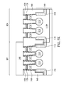
- a substrate 110 is provided, in accordance with some embodiments.
- the substrate 110 includes regions RP and RN, in accordance with some embodiments.
- the region RP is used to form a P-channel metal-oxide-semiconductor field-effect transistor (PMOSFET), in accordance with some embodiments.
- the region RN is used to form an N-channel metal-oxide-semiconductor field-effect transistor (NMOSFET), in accordance with some embodiments.
- PMOSFET P-channel metal-oxide-semiconductor field-effect transistor
- NMOSFET N-channel metal-oxide-semiconductor field-effect transistor
- the substrate 110 includes a semiconductor wafer (such as a silicon wafer) or a portion of a semiconductor wafer.
- the substrate 110 is made of an elementary semiconductor material including silicon or germanium in a single crystal, polycrystal, or amorphous structure.
- the substrate 110 is made of a compound semiconductor, such as silicon carbide, gallium arsenide, gallium phosphide, indium phosphide, indium arsenide, an alloy semiconductor, such as SiGe, or GaAsP, or combinations thereof.
- the substrate 110 may also include multi-layer semiconductors, semiconductor on insulator (SOI) (such as silicon on insulator or germanium on insulator), or combinations thereof.
- SOI semiconductor on insulator
- the substrate 110 is a P-type substrate, in accordance with some embodiments.
- the substrate 110 may include structures such as doped regions, interlayer dielectric (ILD) layers, and/or conductive features.
- the substrate 110 may further include single or multiple material layers.
- the material layers may include a silicon layer, a dielectric layer, and/or a doped polysilicon layer.
- fin structures 115 are formed over the substrate 110 , in accordance with some embodiments.
- the fin structures 115 include the fin structures 112 and 114 , in accordance with some embodiments.
- the fin structures 112 are located over the region RP, in accordance with some embodiments.
- the fin structures 114 are located over the region RN, in accordance with some embodiments.
- the fin structures 112 and 114 are spaced apart from each other, in accordance with some embodiments.
- the fin structures 112 and 114 are formed by patterning the substrate 110 .
- a dielectric layer 120 is formed over upper surfaces 112 a of the fin structures 112 and upper surfaces 114 a of the fin structures 114 , in accordance with some embodiments.
- the dielectric layer 120 includes a dielectric material, in accordance with some embodiments.
- the dielectric material includes oxides, such as silicon oxide, in accordance with some embodiments.
- a mask layer 130 is formed over the dielectric layer 120 , in accordance with some embodiments.
- the mask layer 130 includes a dielectric material, in accordance with some embodiments.
- the dielectric material includes nitrides, such as silicon nitride, in accordance with some embodiments.
- the dielectric layer 120 and the mask layer 130 are made of different materials, in accordance with some embodiments.
- a thickness T 2 of the mask layer 130 is greater than a thickness T 1 of the dielectric layer 120 .
- the thickness T 1 ranges from about 1 nm to about 10 nm, in accordance with some embodiments.
- the thickness T 2 ranges from about 10 nm to about 40 nm, in accordance with some embodiments.
- a mask layer 140 is formed over the region RN of the substrate 110 , in accordance with some embodiments.
- the mask layer 140 covers the fin structures 114 , the dielectric layer 120 over the region RN, and the mask layer 130 over the region RN, in accordance with some embodiments.
- the mask layer 140 is configured to be an implantation mask in a subsequent implantation process, in accordance with some embodiments.
- the mask layer 140 includes a photoresist material, in accordance with some embodiments.
- the mask layer 140 is formed by a coating process and a photolithography process, in accordance with some embodiments.
- the mask layer 140 includes an amorphous carbon material, which is able to sustain high temperatures from about 100° C. to about 500° C., in accordance with some embodiments.
- the mask layer 140 is formed by a deposition process, a photolithography process, and an etching process, in accordance with some embodiments.
- an implantation process is performed on the substrate 110 exposed by the mask layers 130 and 140 to form doped regions 116 in the substrate 110 , in accordance with some embodiments.
- the doped regions 116 are adjacent to the fin structures 112 , in accordance with some embodiments.
- the implantation process includes an ion implantation process, in accordance with some embodiments.
- the implantation process is performed using the mask layers 130 and 140 as an implantation mask, in accordance with some embodiments.
- the doped regions 116 are doped with N-type dopants, in accordance with some embodiments.
- the N-type dopants include phosphorus (P) and/or arsenic (As), in accordance with some embodiments.
- the implantation process is performed at an energy of about 1 keV to about 10 keV, in accordance with some embodiments.
- the implantation energy and the thickness T 2 of the mask layer 130 are adjustable to prevent the dopants from penetrating through the mask layer 130 , in accordance with some embodiments.
- the implantation process is performed at a dose of about 1E13/cm 2 to about 5E14/cm 2 , in accordance with some embodiments.
- the implantation process is performed at room temperature or a higher temperature, such as at about 100° C. to about 500° C., in accordance with some embodiments.
- the mask layer 140 is removed, in accordance with some embodiments.
- the mask layer 140 is removed using a photolithography process, a wet etching process, or a dry etching process, in accordance with some embodiments.
- a mask layer 150 is formed over the region RP of the substrate 110 , in accordance with some embodiments.
- the mask layer 150 covers the fin structures 112 , the dielectric layer 120 over the region RP, and the mask layer 130 over the region RP, in accordance with some embodiments.
- the mask layer 150 is configured to be an implantation mask in a subsequent implantation process, in accordance with some embodiments.
- the mask layer 150 includes a photoresist material, in accordance with some embodiments.
- the mask layer 150 is formed by a coating process and a photolithography process, in accordance with some embodiments.
- the mask layer 150 includes an amorphous carbon material, which is able to sustain high temperatures from about 100° C. to about 500° C., in accordance with some embodiments.
- the mask layer 150 is formed by a deposition process, a photolithography process, and an etching process, in accordance with some embodiments.
- an implantation process is performed on the substrate 110 exposed by the mask layers 130 and 150 to form doped regions 118 in the substrate 110 , in accordance with some embodiments.
- the doped regions 118 are adjacent to the fin structures 114 , in accordance with some embodiments.
- the implantation process includes an ion implantation process, in accordance with some embodiments.
- the implantation process is performed using the mask layers 130 and 150 as an implantation mask, in accordance with some embodiments.
- the doped regions 118 are doped with P-type dopants, in accordance with some embodiments.
- the P-type dopants include boron (B) and/or boron fluoride (BF 2 ), in accordance with some embodiments.
- the implantation process is performed at an energy of about 1 keV to about 10 keV, in accordance with some embodiments.
- the implantation energy and the thickness T 2 of the mask layer 130 are adjustable to prevent the dopants from penetrating through the mask layer 130 , in accordance with some embodiments.
- the implantation process is performed at a dose of about 1E13/cm 2 to about 5E14/cm 2 , in accordance with some embodiments.
- the implantation process is performed at room temperature or a higher temperature, such as at about 100° C. to about 500° C., in accordance with some embodiments.
- the mask layer 150 is removed, in accordance with some embodiments.
- the mask layer 150 is removed using a photolithography process, a wet etching process, or a dry etching process, in accordance with some embodiments.
- a portion of the substrate 110 is removed to define the regions RP and RN, in accordance with some embodiments.
- the removal process forms trenches 119 in the substrate 110 , in accordance with some embodiments.
- the trenches 119 surround the regions RP and RN and separate the region RP from the region RN, in accordance with some embodiments.
- the trenches 119 surround the fin structures 112 and the doped regions 116 , in accordance with some embodiments.
- the trenches 119 surround the fin structures 114 and the doped regions 118 , in accordance with some embodiments.
- the removal process may also remove a portion of the mask layer 130 , in accordance with some embodiments.
- the removal process includes a photolithography process and an etching process, in accordance with some embodiments.
- the substrate 110 has a lower portion 111 and upper portions 113 a and 113 b over the lower portions 111 , in accordance with some embodiments.
- the upper portions 113 a and 113 b are separated from each other by the trenches 119 , in accordance with some embodiments.
- the doped regions 116 are formed in the upper portion 113 a , in accordance with some embodiments.
- the doped regions 118 are formed in the upper portions 113 b , in accordance with some embodiments.
- the width W 1 of the upper portion 113 a (or 113 b ) is less than the width W 2 of the lower portion 111 , in accordance with some embodiments.
- an isolation layer 160 is formed over the substrate 110 , in accordance with some embodiments.
- the isolation layer 160 covers the dielectric layer 120 , the mask layer 130 , the fin structures 112 and 114 , and the substrate 110 , in accordance with some embodiments.
- the isolation layer 160 fills the trenches 119 , in accordance with some embodiments.
- the isolation layer 160 includes silicon oxide or another suitable dielectric material, in accordance with some embodiments.
- the isolation layer 160 is formed by a chemical vapor deposition process, such as a flowable chemical vapor deposition process, in accordance with some embodiments. Thereafter, an annealing process is performed on the isolation layer 160 , in accordance with some embodiments. The annealing process is performed at about 350° C. to about 600° C. for about 10 minutes to about 2 hours, in accordance with some embodiments.
- a planarization process is performed to remove a portion of the isolation layer 160 , in accordance with some embodiments.
- the mask layer 130 is exposed by the isolation layer 160 , in accordance with some embodiments.
- the planarization process includes a chemical mechanical polishing (CMP) process, in accordance with some embodiments.
- CMP chemical mechanical polishing
- an annealing process is performed on the isolation layer 160 , in accordance with some embodiments. The annealing process is performed at about 350° C. to about 600° C. for about 10 minutes to about 2 hours, in accordance with some embodiments.
- the mask layer 130 is removed, in accordance with some embodiments.
- the removal process includes a wet etching process, in accordance with some embodiments.
- a mask layer 170 is formed over the region RN to cover the fin structures 114 and the substrate 110 in the region RN, in accordance with some embodiments.
- the mask layer 170 includes a photoresist material, in accordance with some embodiments.
- the mask layer 170 is formed using a coating process and a photolithography process, in accordance with some embodiments.
- a deep N-well DN is formed in the lower portion 111 in the region RP, in accordance with some embodiments.
- the deep N-well DN is formed using an ion implantation process, in accordance with some embodiments.
- the deep N-well DN is doped with N-type dopants, in accordance with some embodiments.
- the N-type dopants include phosphorus (P) and/or arsenic (As), in accordance with some embodiments.
- the mask layer 170 and the dielectric layer 120 are removed, in accordance with some embodiments.
- the mask layer 170 is removed using a photolithography process, in accordance with some embodiments.
- the dielectric layer 120 is removed by a wet etching process or a dry etching process, in accordance with some embodiments.
- a dielectric layer 180 is formed over the fin structures 112 and 114 , in accordance with some embodiments.
- the dielectric layer 180 is formed using a thermal oxidation process, in accordance with some embodiments.
- a mask layer 190 is formed over the region RP to cover the fin structures 112 and the substrate 110 in the region RP, in accordance with some embodiments.
- the mask layer 190 includes a photoresist material, in accordance with some embodiments.
- the mask layer 190 is formed using a coating process and a photolithography process, in accordance with some embodiments.
- a P-well 117 P is formed in the substrate 110 in the region RN, in accordance with some embodiments.
- the P-well 117 P is also referred to as a P-type doped well.
- the P-well 117 P is formed using an ion implantation process, in accordance with some embodiments.
- the P-well 117 P is doped with P-type dopants, in accordance with some embodiments.
- the P-type dopants include boron (B) and/or boron fluoride (BF 2 ), in accordance with some embodiments.
- the mask layer 190 is removed, in accordance with some embodiments.
- the removal process includes a photolithography process, in accordance with some embodiments.
- a mask layer 210 is formed over the region RN to cover the fin structures 114 and the substrate 110 in the region RN, in accordance with some embodiments.
- the mask layer 210 includes a photoresist material, in accordance with some embodiments.
- the mask layer 210 is formed using a coating process and a photolithography process, in accordance with some embodiments.
- an N-well 117 N is formed in the substrate 110 in the region RP, in accordance with some embodiments.
- the N-well 117 N is also referred to as a N-type doped well.
- the N-well 117 N is formed using an ion implantation process, in accordance with some embodiments.
- the N-well 117 N is doped with N-type dopants, in accordance with some embodiments.
- the N-type dopants include phosphorus (P) and/or arsenic (As), in accordance with some embodiments.
- the mask layer 210 is removed, in accordance with some embodiments.
- the removal process includes a photolithography process, in accordance with some embodiments.
- an annealing process is performed to enlarge the doped regions 116 and 118 , in accordance with some embodiments.
- the doped regions 116 are merged into a merged doped region 116 a
- the doped regions 118 are merged into a merged doped region 118 a , in accordance with some embodiments.
- the merged doped region 116 a is formed in the upper portion 113 a , in accordance with some embodiments.
- the merged doped region 116 a is positioned adjacent to an upper surface P 1 and sidewalls S 1 of the upper portion 113 a , in accordance with some embodiments.
- the merged doped region 116 a is configured to be an anti-punch through region, in accordance with some embodiments.
- the merged doped region 118 a is formed in the upper portion 113 b , in accordance with some embodiments.
- the merged doped region 118 a is positioned adjacent to an upper surface P 2 and sidewalls S 2 of the upper portion 113 b , in accordance with some embodiments.
- the merged doped region 118 a is configured to be an anti-punch through region, in accordance with some embodiments.
- an average dopant concentration of the merged doped region 116 a or 118 a ranges from about 1E18 cm ⁇ 3 to about 1E19 ⁇ 3 .
- the dopants remaining in the substrate 110 exposed by the fin structures 112 are greater in number than the dopants diffusing into the substrate 110 covered by the fin structures 112 .
- a dopant concentration of the merged doped region 116 a exposed by the fin structures 112 is greater than a dopant concentration of the merged doped region 116 a covered by the fin structures 112 , in accordance with some embodiments.
- a dopant concentration of the merged doped region 118 a exposed by the fin structures 114 is greater than a dopant concentration of the merged doped region 118 a covered by the fin structures 114 , in accordance with some embodiments.
- the fin structures 112 have channel regions C 1 over the merged doped region 116 a , in accordance with some embodiments.
- the fin structures 114 have channel regions C 2 over the merged doped region 118 a , in accordance with some embodiments.
- the mask layer 130 may protect the channel regions C 1 and C 2 from being doped and from damage. Therefore, the mask layer 130 may reduce the dopant concentration of the channel regions C 1 and C 2 , which improves carrier mobility in the channel regions C 1 and C 2 . Since the damage resulting from the implantation process is prevented or reduced, the current leakage is reduced.
- an average dopant concentration of the fin structures 112 or 114 ranges from about 1E16 cm ⁇ 3 to about 1E17 cm ⁇ 3 .
- the N-well 117 N is located under the merged doped region 116 a , in accordance with some embodiments.
- the N-well 117 N has a dopant concentration less than the average dopant concentration of the merged doped region 116 a , in accordance with some embodiments.
- the N-well 117 N has a dopant concentration less than the dopant concentration of the merged doped region 116 a covered by the fin structures 112 , in accordance with some embodiments.
- the P-well 117 P is located under the merged doped region 118 a , in accordance with some embodiments.
- the P-well 117 P has a dopant concentration less than the average dopant concentration of the merged doped region 118 a , in accordance with some embodiments.
- the P-well 117 P has a dopant concentration less than the dopant concentration of the merged doped region 118 a covered by the fin structures 114 , in accordance with some embodiments.
- the dielectric layer 180 and an upper portion of the isolation layer 160 are removed, in accordance with some embodiments.
- the sidewalls 112 b of the fin structures 112 and the sidewalls 114 b of the fin structures 114 are partially exposed by the isolation layer 160 , in accordance with some embodiments.
- the isolation layer 160 surrounds the fin structures 112 and 114 , in accordance with some embodiments.
- the isolation layer 160 covers the upper surfaces P 1 , P 2 , and P 3 of the upper portions 113 a and 113 b and the lower portion 111 and the sidewalls S 1 and S 2 of the upper portions 113 a and 113 b , in accordance with some embodiments.
- the removal process includes a dry etching process and/or a wet etching process, in accordance with some embodiments.
- a dummy gate dielectric layer 220 is formed over the fin structures 112 and 114 and the isolation layer 160 , in accordance with some embodiments.
- the dummy gate dielectric layer 220 is made of silicon oxide, in accordance with some embodiments.
- a dummy gate material layer 230 is formed over the dummy gate dielectric layer 220 , in accordance with some embodiments.
- the dummy gate material layer 230 is made of polysilicon, in accordance with some embodiments.
- FIG. 2A is a perspective view of the semiconductor device structure of FIG. 1N , in accordance with some embodiments.
- FIG. 2B is a top view of the semiconductor device structure of FIG. 1N , in accordance with some embodiments.
- FIG. 1N is a cross-sectional view illustrating the semiconductor device structure along a sectional line 1 N- 1 N′ in FIG. 2B , in accordance with some embodiments.
- FIG. 3A is a cross-sectional view illustrating the semiconductor device structure along a sectional line 3 A- 3 A′ in FIG. 2B , in accordance with some embodiments.
- portions of the dummy gate dielectric layer 220 and the dummy gate material layer 230 are removed, in accordance with some embodiments.
- the dummy gate material layer 230 includes dummy gates 232 and 234 , in accordance with some embodiments.
- the dummy gate 232 is over the fin structures 112 , in accordance with some embodiments.
- the dummy gate 234 is over the fin structures 114 , in accordance with some embodiments.
- the removal process includes a photolithography process and an etching process, in accordance with some embodiments.
- FIGS. 3A-3H are cross-sectional views of various stages of a process for forming a semiconductor device structure, in accordance with some embodiments.
- a spacer layer 310 is deposited over the isolation layer 160 to cover the dummy gate dielectric layer 220 and the dummy gate material layer 230 , as shown in FIG. 3B , in accordance with some embodiments.
- the spacer layer 310 includes an insulating material, such as silicon oxide or silicon nitride.
- the spacer layer 310 is formed using a chemical vapor deposition process, in accordance with some embodiments.
- an anisotropic etching process is performed to remove a portion of the spacer layer 310 , in accordance with some embodiments.
- the spacer layer 310 remaining over the sidewalls of the dummy gate material layer 230 and the dummy gate dielectric layer 220 forms spacers 312 , in accordance with some embodiments.
- the spacers 312 are configured to electrically isolate a gate formed subsequently from other devices, in accordance with some embodiments.
- the anisotropic etching process includes a dry etching process, in accordance with some embodiments.
- portions of the fin structures 115 are removed, in accordance with some embodiments.
- recesses 115 a are formed at two opposite sides of the dummy gate material layer 230 , in accordance with some embodiments.
- the removal process includes a photolithography process and an etching process, in accordance with some embodiments.
- doped structures 320 are formed in the recesses 115 a , in accordance with some embodiments.
- the doped structures 320 over the same fin structure 115 include a source structure and a drain structure, in accordance with some embodiments.
- the doped structures 320 include SiGe or SiC, in accordance with some embodiments.
- the doped structures 320 are formed using a selective epitaxial growth (SEG) process, in accordance with some embodiments.
- the doped structures 320 over the fin structure 112 are doped with dopants of an opposite conduction type to the conduction type of the dopants in the merged doped region 116 a , in accordance with some embodiments. That is, the doped structures 320 over the fin structure 112 are doped with P-type dopants, such as boron (B) and/or boron fluoride (BF 2 ), in accordance with some embodiments.
- P-type dopants such as boron (B) and/or boron fluoride (BF 2 ), in accordance with some embodiments.
- the doped structures 320 over the fin structure 114 are doped with dopants of an opposite conduction type to the conduction type of the dopants, which are doped in the merged doped region 118 a , in accordance with some embodiments. That is, the doped structures 320 over the fin structure 114 are doped with N-type dopants, such as boron (B) and/or boron fluoride (BF 2 ), in accordance with some embodiments.
- N-type dopants such as boron (B) and/or boron fluoride (BF 2 ), in accordance with some embodiments.
- the dopant concentration of the doped structures 320 is greater than the average dopant concentration of the merged doped region 116 a or 118 a . In some embodiments, the dopant concentration of the doped structures 320 is greater than the dopant concentration of the merged doped region 116 a exposed by the fin structures 112 (as shown in FIG. 1N ). In some embodiments, the dopant concentration of the doped structures 320 is greater than the dopant concentration of the merged doped region 118 a exposed by the fin structures 114 (as shown in FIG. 1N ).
- the recesses 115 a and the doped structures 320 are not formed. In some other embodiments (not shown), heavy doped regions are formed in the fin structures 115 and at two opposite sides of the dummy gate material layer 230 to serve as source structures and drain structures.
- a contact etch stop layer is formed over the substrate 110 to cover the doped structures 320 , in accordance with some embodiments.
- the contact etch stop layer includes a dielectric material, in accordance with some embodiments.
- the contact etch stop layer includes silicon nitride, in accordance with some embodiments. It should be noted that, for the sake of simplicity, FIG. 3D does not show the contact etch stop layer.
- a dielectric layer 330 is deposited over the substrate 110 , in accordance with some embodiments.
- the dielectric layer 330 covers the isolation layer 160 (as shown in FIG. 2B ), the fin structures 115 , the dummy gate material layer 230 , and the spacers 312 , in accordance with some embodiments.
- the dielectric layer 330 includes silicon oxide, silicon oxynitride, borosilicate glass (BSG), phosphoric silicate glass (PSG), borophosphosilicate glass (BPSG), fluorinated silicate glass (FSG), low-k material, porous dielectric material, or combinations thereof, in accordance with some embodiments.
- the dielectric layer 330 is deposited using a CVD process, a HDPCVD process, a spin-on process, a sputtering process, or a combination thereof, in accordance with some embodiments.
- a planarization process is performed on the dielectric layer 330 until the top surface of the dummy gate material layer 230 is exposed, in accordance with some embodiments.
- the planarization process includes a chemical mechanical polishing (CMP) process, in accordance with some embodiments.
- CMP chemical mechanical polishing
- the dummy gate material layer 230 is removed, in accordance with some embodiments.
- the removal process for removing the dummy gate material layer 230 includes a wet etching process, a dry etching process, or a combination thereof, in accordance with some embodiments.
- the dummy gate dielectric layer 220 is also removed. After the dummy gate material layer 230 and the dummy gate dielectric layer 220 are removed, trenches are formed between the spacers 312 , in accordance with some embodiments.
- FIG. 4A is a perspective view of the semiconductor device structure 300 of FIG. 3H , in accordance with some embodiments.
- FIG. 4B is a top view of the semiconductor device structure 300 of FIG. 3H , in accordance with some embodiments.
- FIG. 3H is a cross-sectional view of the semiconductor device structure 300 along a sectional line 3 H- 3 H′ in FIG. 4B , in accordance with some embodiments.
- FIG. 4C is a cross-sectional view of the semiconductor device structure 300 along a sectional line 4 C- 4 C′ in FIG. 4B , in accordance with some embodiments.
- the trenches include trenches T 1 and T 2 , in accordance with some embodiments.
- the trench T 1 exposes the fin structures 112
- the trench T 2 exposes the fin structures 114 , in accordance with some embodiments.
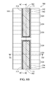
- a gate dielectric layer 342 is formed to cover the bottom of the trench T 1 , in accordance with some embodiments.
- the gate dielectric layer 342 further covers the inner wall of the trench T 1 , in accordance with some embodiments.
- the gate dielectric layer 342 includes a dielectric material, such as a high dielectric constant (high-k) material.
- the high-k material includes hafnium oxide (HfO 2 ), hafnium silicon oxide (HfSiO), hafnium silicon oxynitride (HfSiON), hafnium tantalum oxide (HfTaO), hafnium titanium oxide (HfTiO), hafnium zirconium oxide (HfZrO), other suitable high-k dielectric materials, or combinations thereof.
- the high-k material is made of metal oxides, metal nitrides, metal silicates, transition metal-oxides, transition metal-nitrides, transition metal-silicates, oxynitrides of metals, aluminum oxide, hafnium dioxide-alumina (HfO 2 —Al 2 O 3 ) alloy, other suitable materials, or a combination thereof, in accordance with some embodiments.
- the gate dielectric layer 342 is formed using a deposition process and a planarization process, in accordance with some embodiments.
- the deposition process includes an atomic layer deposition (ALD) process, a chemical vapor deposition (CVD) process, a physical vapor deposition (PVD) process, a sputtering process, a plating process, another suitable process, or a combination thereof, in accordance with some embodiments.
- the gate dielectric layer 342 needs to be annealed.
- An intermediate dielectric layer (not shown) may be formed over the fin structures 112 before the gate dielectric layer 342 is formed.
- the intermediate dielectric layer includes a suitable dielectric material, such as silicon oxide, hafnium silicate, silicon oxynitride, or combinations thereof.
- a work function layer 352 is formed over the gate dielectric layer 342 , in accordance with some embodiments.
- the work function layer 352 provides a desired work function for transistors to enhance device performance including improved threshold voltage.
- the work function layer 352 can be a p-type metal capable of providing a work function value suitable for the device, such as equal to or greater than about 4.8 eV.
- the p-type metal includes metal, metal carbide, metal nitride, other suitable materials, or a combination thereof, in accordance with some embodiments.
- the p-type metal is made of titanium, titanium nitride, other suitable materials, or combinations thereof.
- a gate 362 (also called a metal gate) is formed over the work function layer 352 to fill the trench T 1 , in accordance with some embodiments.
- the gate 362 covers the fin structures 112 , in accordance with some embodiments.
- the gate 362 includes a suitable metal material, such as aluminum, tungsten, gold, platinum, cobalt, another suitable metal, an alloy thereof, or combinations thereof, in accordance with some embodiments.
- the gate 362 is formed using a deposition process and a planarization process, in accordance with some embodiments.
- the deposition process includes an atomic layer deposition (ALD) process and a chemical vapor deposition (CVD) process, in accordance with some embodiments.
- ALD atomic layer deposition
- CVD chemical vapor deposition
- the gate 362 is deposited using a PVD process, a plating process, or the like, or a combination thereof.
- a gate dielectric layer 344 is formed to cover the bottom of the trench T 2 , in accordance with some embodiments.
- the gate dielectric layer 344 further covers the inner wall of the trench T 2 , in accordance with some embodiments.
- the gate dielectric layers 344 and 342 are made of the same material, in accordance with some embodiments.
- a work function layer 354 is formed over the gate dielectric layer 344 , in accordance with some embodiments.
- the work function layer 354 provides a desired work function for transistors to enhance device performance including improved threshold voltage.
- the work function layer 354 can be an n-type metal capable of providing a work function value suitable for the device, such as equal to or less than about 4.5 eV.
- the n-type metal includes metal, metal carbide, metal nitride, or combinations thereof, in accordance with some embodiments.
- the n-type metal is made of tantalum, tantalum nitride, or combinations thereof.
- a gate 364 (also called a metal gate material layer) is formed over the work function layer 354 to fill the trench T 2 , in accordance with some embodiments.
- the gate 364 covers the fin structures 114 , in accordance with some embodiments.
- the gate 364 includes a suitable metal material, such as aluminum, tungsten, gold, platinum, cobalt, another suitable metal, an alloy thereof, or combinations thereof, in accordance with some embodiments.
- the gate 364 is formed using a deposition process and a planarization process, in accordance with some embodiments.
- the deposition process includes an atomic layer deposition (ALD) process and a chemical vapor deposition (CVD) process, in accordance with some embodiments.
- ALD atomic layer deposition
- CVD chemical vapor deposition
- the gate 364 is deposited using a PVD process, a plating process, or the like, or a combination thereof.
- FIGS. 5A-5Q are cross-sectional views of various stages of a process for forming a semiconductor device structure, in accordance with some embodiments.
- a substrate 110 is provided, in accordance with some embodiments.
- the substrate 110 includes regions RP and RN, in accordance with some embodiments.
- the region RP is used to form a P-channel metal-oxide-semiconductor field-effect transistor (PMOSFET), in accordance with some embodiments.
- the region RN is used to form an N-channel metal-oxide-semiconductor field-effect transistor (NMOSFET), in accordance with some embodiments.
- PMOSFET P-channel metal-oxide-semiconductor field-effect transistor
- NMOSFET N-channel metal-oxide-semiconductor field-effect transistor
- the substrate 110 has trenches 119 , in accordance with some embodiments.
- the trenches 119 surround the regions RP and RN, in accordance with some embodiments.
- the substrate 110 has a lower portion 111 and upper portions 113 a and 113 b over the lower portions 111 , in accordance with some embodiments.
- the upper portions 113 a and 113 b are located in the regions RP and RN, respectively, in accordance with some embodiments.
- the upper portions 113 a and 113 b are separated from each other by the trenches 119 , in accordance with some embodiments.
- fin structures 115 are formed over the substrate 110 , in accordance with some embodiments.
- the fin structures 115 include the fin structures 112 and 114 , in accordance with some embodiments.
- the fin structures 112 are located over the upper portion 113 a , in accordance with some embodiments.
- the fin structures 114 are located over the upper portion 113 b , in accordance with some embodiments.
- the fin structures 112 and 114 are spaced apart from each other, in accordance with some embodiments.
- the fin structures 112 and 114 are formed by patterning the substrate 110 .
- a dielectric layer 120 is formed over upper surfaces 112 a of the fin structures 112 and upper surfaces 114 a of the fin structures 114 , in accordance with some embodiments.
- the dielectric layer 120 includes a dielectric material, in accordance with some embodiments.
- the dielectric material includes oxides, such as silicon oxide, in accordance with some embodiments.
- a mask layer 130 is formed over the dielectric layer 120 , in accordance with some embodiments.
- the mask layer 130 includes a dielectric material, in accordance with some embodiments.
- the dielectric material includes nitrides, such as silicon nitride, in accordance with some embodiments.
- the dielectric layer 120 and the mask layer 130 are made of different materials, in accordance with some embodiments.
- a mask layer 140 is formed over the region RN of the substrate 110 , in accordance with some embodiments.
- the mask layer 140 covers the fin structures 114 , the dielectric layer 120 and the mask layer 130 over the region RN, and the upper portion 113 b , in accordance with some embodiments.
- the mask layer 140 is configured to be an implantation mask in a subsequent implantation process, in accordance with some embodiments.
- an implantation process is performed on the substrate 110 exposed by the mask layers 130 and 140 to form doped regions 116 in the substrate 110 , in accordance with some embodiments.
- the doped regions 116 are adjacent to the fin structures 112 , in accordance with some embodiments.
- the doped regions 116 are formed in the upper portion 113 a , in accordance with some embodiments.
- a portion of the doped regions 116 are formed in the lower portion 111 , in accordance with some embodiments.
- the width W 1 of the upper portion 113 a (or 113 b ) is less than the width W 2 of the lower portion 111 , in accordance with some embodiments.
- the implantation process includes an ion implantation process, in accordance with some embodiments.
- the implantation process is performed using the mask layers 130 and 140 as an implantation mask, in accordance with some embodiments.
- the doped regions 116 are doped with N-type dopants, in accordance with some embodiments.
- the N-type dopants include phosphorus (P) and/or arsenic (As), in accordance with some embodiments.
- the implantation process is performed at an energy of about 1 keV to about 13 keV, in accordance with some embodiments.
- the implantation energy and the thickness T 2 of the mask layer 130 are adjustable to prevent the dopants from penetrating through the mask layer 130 , in accordance with some embodiments.
- the implantation process is performed at a dose of about 1E13/cm 2 to about 5E14/cm 2 , in accordance with some embodiments.
- the implantation process is performed at room temperature or a higher temperature, such as at about 100° C. to about 500° C., in accordance with some embodiments.
- the mask layer 140 is removed, in accordance with some embodiments.
- the mask layer 140 is removed using a photolithography process, a wet etching process, or a dry etching process, in accordance with some embodiments.
- a mask layer 150 is formed over the region RP of the substrate 110 , in accordance with some embodiments.
- the mask layer 150 covers the fin structures 112 and the dielectric layer 120 and the mask layer 130 over the region RP, in accordance with some embodiments.
- the mask layer 150 is configured to be an implantation mask in a subsequent implantation process, in accordance with some embodiments.
- the mask layer 150 includes a photoresist material, in accordance with some embodiments.
- the mask layer 150 is formed by a coating process and a photolithography process, in accordance with some embodiments.
- the mask layer 150 includes an amorphous carbon material, which is able to sustain high temperatures from about 100° C. to about 500° C., in accordance with some embodiments.
- the mask layer 150 is formed by a deposition process, a photolithography process, and an etching process, in accordance with some embodiments.
- an implantation process is performed on the substrate 110 exposed by the mask layers 130 and 150 to form doped regions 118 in the substrate 110 , in accordance with some embodiments.
- the doped regions 118 are adjacent to the fin structures 114 , in accordance with some embodiments.
- the doped regions 118 are formed in the upper portions 113 b , in accordance with some embodiments.
- a portion of the doped regions 118 are formed in the lower 111 , in accordance with some embodiments.
- the implantation process includes an ion implantation process, in accordance with some embodiments.
- the implantation process is performed using the mask layers 130 and 150 as an implantation mask, in accordance with some embodiments.
- the doped regions 118 are doped with P-type dopants, in accordance with some embodiments.
- the P-type dopants include boron (B) and/or boron fluoride (BF 2 ), in accordance with some embodiments.
- the implantation process is performed at an energy of about 1 keV to about 7 keV, in accordance with some embodiments.
- the implantation energy and the thickness T 2 of the mask layer 130 are adjustable to prevent the dopants from penetrating through the mask layer 130 , in accordance with some embodiments.
- the implantation process is performed at a dose of about 1E13/cm 2 to about 5E14/cm 2 , in accordance with some embodiments.
- the implantation process is performed at room temperature or a higher temperature, such as at about 100° C. to about 500° C., in accordance with some embodiments.
- the mask layer 150 is removed, in accordance with some embodiments.
- the mask layer 150 is removed using a photolithography process, a wet etching process, or a dry etching process, in accordance with some embodiments.
- a diffusion layer 510 is formed over the substrate 110 to cover the substrate 110 exposed by the fin structures 112 , in accordance with some embodiments.
- the diffusion layer 510 covers the dielectric layer 120 , the mask layer 130 , the fin structures 112 and 114 , and the substrate 110 , in accordance with some embodiments.
- the diffusion layer 510 conformally covers the sidewalls 112 b of the fin structures 112 , the upper surface P 1 and the sidewalls S 1 of the upper portion 113 a , and the upper surface P 3 of the lower portion 111 , in accordance with some embodiments.
- the diffusion layer 510 is in direct contact with the substrate 110 and the fin structure 112 , in accordance with some embodiments.
- the diffusion layer 510 is configured to be a solid phase diffusion source, in accordance with some embodiments.
- the diffusion layer 510 includes a phosphor-silicate glass (PSG) layer or another suitable material layer with N-type dopants, in accordance with some embodiments.
- PSG phosphor-silicate glass
- the diffusion layer 510 has a thickness T 3 ranging from about 1 nm to about 5 nm, in accordance with some embodiments.
- the diffusion layer 510 is formed using a chemical vapor deposition process, in accordance with some embodiments. In some embodiments, before the formation of the diffusion layer 510 , a cleaning process is performed to remove the native oxide layer over the substrate 110 and the fin structures 112 and 114 .
- a mask layer 520 is formed over the region RP to cover the diffusion layer 510 , in accordance with some embodiments.
- the mask layer 520 includes a photoresist material, in accordance with some embodiments.
- the mask layer 520 is formed using a coating process and a photolithography process, in accordance with some embodiments.
- the diffusion layer 510 over the region RN is removed, in accordance with some embodiments.
- the removal process includes a dry etching process, a wet etching process, or another suitable process.
- the mask layer 520 is removed, in accordance with some embodiments.
- a diffusion layer 530 is formed over the substrate 110 to cover the substrate 110 exposed by the fin structures 114 , in accordance with some embodiments.
- the diffusion layer 530 covers the dielectric layer 120 , the mask layer 130 , the diffusion layer 510 , the fin structures 114 , and the substrate 110 , in accordance with some embodiments.
- the diffusion layer 530 conformally covers the sidewalls 114 b of the fin structures 114 , the upper surface P 2 and the sidewalls S 2 of the upper portion 113 b , and the upper surface P 3 of the lower portion 111 , in accordance with some embodiments.
- the diffusion layer 530 is in direct contact with the substrate 110 and the fin structure 114 , in accordance with some embodiments.
- the diffusion layer 530 is configured to be a solid phase diffusion source, in accordance with some embodiments.
- the diffusion layer 530 includes a borosilicate glass (BSG) layer or another suitable material layer with P-type dopants, in accordance with some embodiments.
- BSG borosilicate glass
- the diffusion layer 530 has a thickness T 4 ranging from about 1 nm to about 5 nm, in accordance with some embodiments.
- the diffusion layer 530 is formed using a chemical vapor deposition process, in accordance with some embodiments.
- an isolation layer 160 is formed over the diffusion layer 530 , in accordance with some embodiments.
- the isolation layer 160 covers the dielectric layer 120 , the mask layer 130 , the fin structures 112 and 114 , and the substrate 110 , in accordance with some embodiments.
- the isolation layer 160 fills the trenches 119 , in accordance with some embodiments.
- the isolation layer 160 includes silicon oxide or another suitable dielectric material, in accordance with some embodiments.
- the isolation layer 160 is formed by a chemical vapor deposition process, such as a flowable chemical vapor deposition process, in accordance with some embodiments. Thereafter, an annealing process is performed on the isolation layer 160 , in accordance with some embodiments. The annealing process is performed at about 350° C. to about 600° C. for about 10 minutes to about 2 hours, in accordance with some embodiments.
- a planarization process is performed to remove a portion of the isolation layer 160 and portions of the diffusion layers 510 and 530 , in accordance with some embodiments.
- the mask layer 130 is exposed by the isolation layer 160 , in accordance with some embodiments.
- the planarization process includes a chemical mechanical polishing (CMP) process, in accordance with some embodiments. Thereafter, an annealing process is performed on the isolation layer 160 , in accordance with some embodiments. The annealing process is performed at about 350° C. to about 600° C. for about 10 minutes to about 2 hours, in accordance with some embodiments.
- CMP chemical mechanical polishing
- the mask layer 130 is removed, in accordance with some embodiments.
- the removal process includes a wet etching process, in accordance with some embodiments.
- a mask layer 190 is formed over the region RP to cover the fin structures 112 and the substrate 110 in the region RP, in accordance with some embodiments.
- the mask layer 190 includes a photoresist material, in accordance with some embodiments.
- the mask layer 190 is formed using a coating process and a photolithography process, in accordance with some embodiments.
- a P-well 117 P is formed in the substrate 110 in the region RN, in accordance with some embodiments.
- the P-well 117 P is formed using an ion implantation process, in accordance with some embodiments.
- the P-well 117 P is doped with P-type dopants, in accordance with some embodiments.
- the P-type dopants include boron (B) and/or boron fluoride (BF 2 ), in accordance with some embodiments.
- the mask layer 190 is removed, in accordance with some embodiments.
- the removal process includes a photolithography process, in accordance with some embodiments.
- a mask layer 210 is formed over the region RN to cover the fin structures 114 and the substrate 110 in the region RN, in accordance with some embodiments.
- the mask layer 210 includes a photoresist material, in accordance with some embodiments.
- the mask layer 210 is formed using a coating process and a photolithography process, in accordance with some embodiments.
- an N-well 117 N is formed in the substrate 110 in the region RP, in accordance with some embodiments.
- the N-well 117 N is formed using an ion implantation process, in accordance with some embodiments.
- the N-well 117 N is doped with N-type dopants, in accordance with some embodiments.
- the N-type dopants include phosphorus (P) and/or arsenic (As), in accordance with some embodiments.
- the mask layer 210 is removed, in accordance with some embodiments.
- the removal process includes a photolithography process, in accordance with some embodiments.
- the dielectric layer 120 , an upper portion of the isolation layer 160 , and upper portions of the diffusion layers 510 and 530 are removed, in accordance with some embodiments.
- the removal process includes a dry etching process and/or a wet etching process, in accordance with some embodiments.
- an annealing process is performed to enlarge the doped regions 116 and 118 , in accordance with some embodiments.
- the annealing process is performed at from about 1000° C. to about 1100° C. for about 1 second to about 10 seconds, in accordance with some embodiments.
- an average dopant concentration of the merged doped region 116 a or 118 a ranges from about 1E18 cm ⁇ 3 to about 1E19 ⁇ 3 .
- the dopants remaining in the substrate 110 exposed by the fin structures 112 are greater in number than the dopants diffusing into the substrate 110 covered by the fin structures 112 .
- a dopant concentration of the merged doped region 116 a exposed by the fin structures 112 is greater than a dopant concentration of the merged doped region 116 a covered by the fin structures 112 , in accordance with some embodiments.
- a dopant concentration of the merged doped region 118 a exposed by the fin structures 114 is greater than a dopant concentration of the merged doped region 118 a covered by the fin structures 114 , in accordance with some embodiments.
- a portion of the dopants in the diffusion layer 510 may diffuse into the merged doped region 116 a to increase the dopant concentration of the merged doped region 116 a , in accordance with some embodiments.
- a portion of the dopants in the diffusion layer 530 may diffuse into the merged doped region 118 a to increase the dopant concentration of the merged doped region 118 a , in accordance with some embodiments.
- an average dopant concentration of the fin structures 112 or 114 ranges from about 1E16 cm ⁇ 3 to about 1E17 ⁇ 3 .
- a dummy gate dielectric layer 220 is formed over the fin structures 112 and 114 and the isolation layer 160 , in accordance with some embodiments.
- the dummy gate dielectric layer 220 is made of silicon oxide, in accordance with some embodiments.
- a dummy gate material layer 230 is formed over the dummy gate dielectric layer 220 , in accordance with some embodiments.
- the dummy gate material layer 230 is made of polysilicon, in accordance with some embodiments.
- FIG. 6A is a perspective view of the semiconductor device structure of FIG. 5Q , in accordance with some embodiments.
- FIG. 6B is a top view of the semiconductor device structure of FIG. 5Q , in accordance with some embodiments.
- FIG. 5Q is a cross-sectional view illustrating the semiconductor device structure along a sectional line 5 Q- 5 Q′ in FIG. 6B , in accordance with some embodiments.
- FIG. 7A is a cross-sectional view illustrating the semiconductor device structure along a sectional line 7 A- 7 A′ in FIG. 6B , in accordance with some embodiments.
- portions of the dummy gate dielectric layer 220 and the dummy gate material layer 230 are removed, in accordance with some embodiments.
- the dummy gate material layer 230 includes dummy gates 232 and 234 , in accordance with some embodiments.
- the dummy gate 232 is over the fin structures 112 , in accordance with some embodiments.
- the dummy gate 234 is over the fin structures 114 , in accordance with some embodiments.
- the removal process includes a photolithography process and an etching process, in accordance with some embodiments.
- FIGS. 7A-7B are cross-sectional views of various stages of a process for forming a semiconductor device structure, in accordance with some embodiments.
- FIG. 8A is a perspective view of the semiconductor device structure 700 of FIG. 7B , in accordance with some embodiments.
- FIG. 8B is a top view of the semiconductor device structure 700 of FIG. 7B , in accordance with some embodiments.
- FIG. 7B is a cross-sectional view of the semiconductor device structure 700 along a sectional line 7 B- 7 B′ in FIG. 8B , in accordance with some embodiments.
- FIG. 8C is a cross-sectional view of the semiconductor device structure 700 along a sectional line 8 C- 8 C′ in FIG. 8B , in accordance with some embodiments.
- FIGS. 7B, 8A, 8B, and 8C after the stage of FIG. 7A , stages similar to (or the same as) the stages of FIGS. 3B-3H are performed and a semiconductor device structure 700 is formed, in accordance with some embodiments.
- the semiconductor device structure 700 is substantially similar to the semiconductor device structure 300 (as shown in FIGS. 3H and 4A-4C ), except that the semiconductor device structure 700 further includes the diffusion layers 510 and 530 , in accordance with some embodiments.
- the diffusion layer 510 is positioned over the substrate 110 and lower portions of the sidewalls 112 b of the fin structures 112 , in accordance with some embodiments.
- the diffusion layer 510 surrounds the fin structures 112 , in accordance with some embodiments.
- the diffusion layer 510 includes dopants, and the dopants of the diffusion layer 510 and the dopants of the merged doped region 116 a are made of the same material (such as N-type materials), in accordance with some embodiments.
- the diffusion layer 530 is positioned over the substrate 110 and lower portions of the sidewalls 114 b of the fin structures 114 , in accordance with some embodiments.
- the diffusion layer 530 surrounds the fin structures 114 , in accordance with some embodiments.
- the diffusion layer 530 further surrounds the fin structures 112 and the diffusion layer 510 , in accordance with some embodiments.
- the diffusion layer 530 includes dopants, and the dopants of the diffusion layer 530 and the dopants of the merged doped region 118 a are made of the same material (such as P-type materials), in accordance with some embodiments.
- semiconductor device structures and methods for forming the same are provided.
- the methods (for forming the semiconductor device structure) form a mask layer over fin structures before the implantation process to protect channel regions of the fin structures from being doped and from damage during the implantation process. Therefore, the mask layer reduces the dopant concentration of the channel regions, which improves carrier mobility in the channel regions. Since the damage resulting from the implantation process is prevented or reduced, the current leakage is reduced.
- a semiconductor device structure includes a substrate having a doped region in an upper portion of the substrate.
- the doped region is doped with first dopants of a first conduction type.
- the semiconductor device structure includes one fin structure over the substrate. A first dopant concentration of the doped region exposed by the fin structure is greater than a second dopant concentration of the doped region covered by the fin structure.
- the semiconductor device structure includes an isolation layer over the substrate and at two opposite sides of the fin structure.
- the semiconductor device structure includes a gate over the isolation layer and the fin structure.
- a semiconductor device structure includes a substrate having a doped region in an upper portion of the substrate.
- the doped region is doped with first dopants of a first conduction type.
- the semiconductor device structure includes at least one fin structure over the substrate.
- the semiconductor device structure includes a first diffusion layer over the substrate and a first lower portion of a first sidewall of the fin structure.
- the first diffusion layer includes second dopants, and the second dopants and the first dopants are made of a same material.
- the semiconductor device structure includes an isolation layer over the first diffusion layer.
- the semiconductor device structure includes a gate over the isolation layer and the fin structure.
- a method for forming a semiconductor device structure includes providing a substrate, a fin structure, a dielectric layer, and a mask layer.
- the fin structure is over the substrate, the dielectric layer is over the fin structure, and the mask layer is over the dielectric layer.
- the method includes performing an implantation process on the substrate exposed by the mask layer to form doped regions in the substrate.
- the method includes forming an isolation layer over the substrate.
- the method includes removing the dielectric layer and the mask layer.
- the method includes performing an annealing process on the substrate to enlarge the doped regions so as to merge the doped regions into a merged doped region.
- the method includes form a gate over the fin structure and the isolation layer.
Landscapes
- Engineering & Computer Science (AREA)
- Power Engineering (AREA)
- Microelectronics & Electronic Packaging (AREA)
- Physics & Mathematics (AREA)
- General Physics & Mathematics (AREA)
- Computer Hardware Design (AREA)
- Condensed Matter Physics & Semiconductors (AREA)
- Manufacturing & Machinery (AREA)
- Ceramic Engineering (AREA)
- High Energy & Nuclear Physics (AREA)
- Health & Medical Sciences (AREA)
- Toxicology (AREA)
- Insulated Gate Type Field-Effect Transistor (AREA)
Abstract
A semiconductor device structure is provided. The semiconductor device structure includes a substrate having a doped region in an upper portion of the substrate. The doped region is doped with first dopants of a first conduction type. The semiconductor device structure includes one fin structure over the substrate. A first dopant concentration of the doped region exposed by the fin structure is greater than a second dopant concentration of the doped region covered by the fin structure. The semiconductor device structure includes an isolation layer over the substrate and at two opposite sides of the fin structure. The semiconductor device structure includes a gate over the isolation layer and the fin structure.
Description
The semiconductor integrated circuit (IC) industry has experienced rapid growth. Technological advances in IC materials and design have produced generations of ICs. Each generation has smaller and more complex circuits than the previous generation. However, these advances have increased the complexity of processing and manufacturing ICs.
In the course of IC evolution, functional density (i.e., the number of interconnected devices per chip area) has generally increased while geometric size (i.e., the smallest component (or line) that can be created using a fabrication process) has decreased. This scaling-down process generally provides benefits by increasing production efficiency and lowering associated costs.
However, since feature sizes continue to decrease, fabrication processes continue to become more difficult to perform. Therefore, it is a challenge to form reliable semiconductor devices at smaller and smaller sizes.
Aspects of the present disclosure are best understood from the following detailed description when read with the accompanying figures. It should be noted that, in accordance with standard practice in the industry, various features are not drawn to scale. In fact, the dimensions of the various features may be arbitrarily increased or reduced for clarity of discussion.
The following disclosure provides many different embodiments, or examples, for implementing different features of the subject matter provided. Specific examples of components and arrangements are described below to simplify the present disclosure. These are, of course, merely examples and are not intended to be limiting. For example, the formation of a first feature over or on a second feature in the description that follows may include embodiments in which the first and second features are formed in direct contact, and may also include embodiments in which additional features may be formed between the first and second features, such that the first and second features may not be in direct contact. In addition, the present disclosure may repeat reference numerals and/or letters in the various examples. This repetition is for the purpose of simplicity and clarity and does not in itself dictate a relationship between the various embodiments and/or configurations discussed.
Further, spatially relative terms, such as “beneath,” “below,” “lower,” “above,” “upper” and the like, may be used herein for ease of description to describe one element or feature's relationship to another element(s) or feature(s) as illustrated in the figures. The spatially relative terms are intended to encompass different orientations of the device in use or operation in addition to the orientation depicted in the figures. The apparatus may be otherwise oriented (rotated 90 degrees or at other orientations) and the spatially relative descriptors used herein may likewise be interpreted accordingly. It should be understood that additional operations can be provided before, during, and after the method, and some of the operations described can be replaced or eliminated for other embodiments of the method.
The substrate 110 includes a semiconductor wafer (such as a silicon wafer) or a portion of a semiconductor wafer. In some embodiments, the substrate 110 is made of an elementary semiconductor material including silicon or germanium in a single crystal, polycrystal, or amorphous structure.
In some other embodiments, the substrate 110 is made of a compound semiconductor, such as silicon carbide, gallium arsenide, gallium phosphide, indium phosphide, indium arsenide, an alloy semiconductor, such as SiGe, or GaAsP, or combinations thereof. The substrate 110 may also include multi-layer semiconductors, semiconductor on insulator (SOI) (such as silicon on insulator or germanium on insulator), or combinations thereof. The substrate 110 is a P-type substrate, in accordance with some embodiments.
In addition, the substrate 110 may include structures such as doped regions, interlayer dielectric (ILD) layers, and/or conductive features. Furthermore, the substrate 110 may further include single or multiple material layers. For example, the material layers may include a silicon layer, a dielectric layer, and/or a doped polysilicon layer.
As shown in FIG. 1A , fin structures 115 are formed over the substrate 110, in accordance with some embodiments. The fin structures 115 include the fin structures 112 and 114, in accordance with some embodiments. The fin structures 112 are located over the region RP, in accordance with some embodiments. The fin structures 114 are located over the region RN, in accordance with some embodiments. The fin structures 112 and 114 are spaced apart from each other, in accordance with some embodiments. In some embodiments, the fin structures 112 and 114 are formed by patterning the substrate 110.
As shown in FIG. 1A , a dielectric layer 120 is formed over upper surfaces 112 a of the fin structures 112 and upper surfaces 114 a of the fin structures 114, in accordance with some embodiments. The dielectric layer 120 includes a dielectric material, in accordance with some embodiments. The dielectric material includes oxides, such as silicon oxide, in accordance with some embodiments.
As shown in FIG. 1A , a mask layer 130 is formed over the dielectric layer 120, in accordance with some embodiments. The mask layer 130 includes a dielectric material, in accordance with some embodiments. The dielectric material includes nitrides, such as silicon nitride, in accordance with some embodiments. The dielectric layer 120 and the mask layer 130 are made of different materials, in accordance with some embodiments.
In some embodiments, a thickness T2 of the mask layer 130 is greater than a thickness T1 of the dielectric layer 120. The thickness T1 ranges from about 1 nm to about 10 nm, in accordance with some embodiments. The thickness T2 ranges from about 10 nm to about 40 nm, in accordance with some embodiments.
As shown in FIG. 1B , a mask layer 140 is formed over the region RN of the substrate 110, in accordance with some embodiments. The mask layer 140 covers the fin structures 114, the dielectric layer 120 over the region RN, and the mask layer 130 over the region RN, in accordance with some embodiments. The mask layer 140 is configured to be an implantation mask in a subsequent implantation process, in accordance with some embodiments.
The mask layer 140 includes a photoresist material, in accordance with some embodiments. The mask layer 140 is formed by a coating process and a photolithography process, in accordance with some embodiments. The mask layer 140 includes an amorphous carbon material, which is able to sustain high temperatures from about 100° C. to about 500° C., in accordance with some embodiments. The mask layer 140 is formed by a deposition process, a photolithography process, and an etching process, in accordance with some embodiments.
As shown in FIG. 1B , an implantation process is performed on the substrate 110 exposed by the mask layers 130 and 140 to form doped regions 116 in the substrate 110, in accordance with some embodiments. The doped regions 116 are adjacent to the fin structures 112, in accordance with some embodiments. The implantation process includes an ion implantation process, in accordance with some embodiments.
The implantation process is performed using the mask layers 130 and 140 as an implantation mask, in accordance with some embodiments. The doped regions 116 are doped with N-type dopants, in accordance with some embodiments. The N-type dopants include phosphorus (P) and/or arsenic (As), in accordance with some embodiments.
The implantation process is performed at an energy of about 1 keV to about 10 keV, in accordance with some embodiments. The implantation energy and the thickness T2 of the mask layer 130 are adjustable to prevent the dopants from penetrating through the mask layer 130, in accordance with some embodiments. The implantation process is performed at a dose of about 1E13/cm2 to about 5E14/cm2, in accordance with some embodiments. The implantation process is performed at room temperature or a higher temperature, such as at about 100° C. to about 500° C., in accordance with some embodiments.
As shown in FIG. 1C , the mask layer 140 is removed, in accordance with some embodiments. The mask layer 140 is removed using a photolithography process, a wet etching process, or a dry etching process, in accordance with some embodiments. As shown in FIG. 1C , a mask layer 150 is formed over the region RP of the substrate 110, in accordance with some embodiments.
The mask layer 150 covers the fin structures 112, the dielectric layer 120 over the region RP, and the mask layer 130 over the region RP, in accordance with some embodiments. The mask layer 150 is configured to be an implantation mask in a subsequent implantation process, in accordance with some embodiments.
The mask layer 150 includes a photoresist material, in accordance with some embodiments. The mask layer 150 is formed by a coating process and a photolithography process, in accordance with some embodiments. The mask layer 150 includes an amorphous carbon material, which is able to sustain high temperatures from about 100° C. to about 500° C., in accordance with some embodiments. The mask layer 150 is formed by a deposition process, a photolithography process, and an etching process, in accordance with some embodiments.
As shown in FIG. 1C , an implantation process is performed on the substrate 110 exposed by the mask layers 130 and 150 to form doped regions 118 in the substrate 110, in accordance with some embodiments. The doped regions 118 are adjacent to the fin structures 114, in accordance with some embodiments. The implantation process includes an ion implantation process, in accordance with some embodiments.
The implantation process is performed using the mask layers 130 and 150 as an implantation mask, in accordance with some embodiments. The doped regions 118 are doped with P-type dopants, in accordance with some embodiments. The P-type dopants include boron (B) and/or boron fluoride (BF2), in accordance with some embodiments.
The implantation process is performed at an energy of about 1 keV to about 10 keV, in accordance with some embodiments. The implantation energy and the thickness T2 of the mask layer 130 are adjustable to prevent the dopants from penetrating through the mask layer 130, in accordance with some embodiments. The implantation process is performed at a dose of about 1E13/cm2 to about 5E14/cm2, in accordance with some embodiments. The implantation process is performed at room temperature or a higher temperature, such as at about 100° C. to about 500° C., in accordance with some embodiments.
As shown in FIG. 1D , the mask layer 150 is removed, in accordance with some embodiments. The mask layer 150 is removed using a photolithography process, a wet etching process, or a dry etching process, in accordance with some embodiments. As shown in FIG. 1D , a portion of the substrate 110 is removed to define the regions RP and RN, in accordance with some embodiments. The removal process forms trenches 119 in the substrate 110, in accordance with some embodiments.
The trenches 119 surround the regions RP and RN and separate the region RP from the region RN, in accordance with some embodiments. The trenches 119 surround the fin structures 112 and the doped regions 116, in accordance with some embodiments. The trenches 119 surround the fin structures 114 and the doped regions 118, in accordance with some embodiments. The removal process may also remove a portion of the mask layer 130, in accordance with some embodiments. The removal process includes a photolithography process and an etching process, in accordance with some embodiments.
After the removal process, the substrate 110 has a lower portion 111 and upper portions 113 a and 113 b over the lower portions 111, in accordance with some embodiments. The upper portions 113 a and 113 b are separated from each other by the trenches 119, in accordance with some embodiments.
The doped regions 116 are formed in the upper portion 113 a, in accordance with some embodiments. The doped regions 118 are formed in the upper portions 113 b, in accordance with some embodiments. The width W1 of the upper portion 113 a (or 113 b) is less than the width W2 of the lower portion 111, in accordance with some embodiments.
As shown in FIG. 1E , an isolation layer 160 is formed over the substrate 110, in accordance with some embodiments. The isolation layer 160 covers the dielectric layer 120, the mask layer 130, the fin structures 112 and 114, and the substrate 110, in accordance with some embodiments. The isolation layer 160 fills the trenches 119, in accordance with some embodiments. The isolation layer 160 includes silicon oxide or another suitable dielectric material, in accordance with some embodiments.
The isolation layer 160 is formed by a chemical vapor deposition process, such as a flowable chemical vapor deposition process, in accordance with some embodiments. Thereafter, an annealing process is performed on the isolation layer 160, in accordance with some embodiments. The annealing process is performed at about 350° C. to about 600° C. for about 10 minutes to about 2 hours, in accordance with some embodiments.
As shown in FIG. 1F , a planarization process is performed to remove a portion of the isolation layer 160, in accordance with some embodiments. The mask layer 130 is exposed by the isolation layer 160, in accordance with some embodiments. The planarization process includes a chemical mechanical polishing (CMP) process, in accordance with some embodiments. Thereafter, an annealing process is performed on the isolation layer 160, in accordance with some embodiments. The annealing process is performed at about 350° C. to about 600° C. for about 10 minutes to about 2 hours, in accordance with some embodiments.
As shown in FIG. 1G , the mask layer 130 is removed, in accordance with some embodiments. The removal process includes a wet etching process, in accordance with some embodiments. As shown in FIG. 1G , a mask layer 170 is formed over the region RN to cover the fin structures 114 and the substrate 110 in the region RN, in accordance with some embodiments. The mask layer 170 includes a photoresist material, in accordance with some embodiments. The mask layer 170 is formed using a coating process and a photolithography process, in accordance with some embodiments.
As shown in FIG. 1G , a deep N-well DN is formed in the lower portion 111 in the region RP, in accordance with some embodiments. The deep N-well DN is formed using an ion implantation process, in accordance with some embodiments. The deep N-well DN is doped with N-type dopants, in accordance with some embodiments. The N-type dopants include phosphorus (P) and/or arsenic (As), in accordance with some embodiments.
As shown in FIG. 1H , the mask layer 170 and the dielectric layer 120 are removed, in accordance with some embodiments. The mask layer 170 is removed using a photolithography process, in accordance with some embodiments. The dielectric layer 120 is removed by a wet etching process or a dry etching process, in accordance with some embodiments. As shown in FIG. 1I , a dielectric layer 180 is formed over the fin structures 112 and 114, in accordance with some embodiments. The dielectric layer 180 is formed using a thermal oxidation process, in accordance with some embodiments.
As shown in FIG. 1I , a mask layer 190 is formed over the region RP to cover the fin structures 112 and the substrate 110 in the region RP, in accordance with some embodiments. The mask layer 190 includes a photoresist material, in accordance with some embodiments. The mask layer 190 is formed using a coating process and a photolithography process, in accordance with some embodiments.
As shown in FIG. 1I , a P-well 117P is formed in the substrate 110 in the region RN, in accordance with some embodiments. The P-well 117P is also referred to as a P-type doped well. The P-well 117P is formed using an ion implantation process, in accordance with some embodiments. The P-well 117P is doped with P-type dopants, in accordance with some embodiments. The P-type dopants include boron (B) and/or boron fluoride (BF2), in accordance with some embodiments.
As shown in FIG. 1J , the mask layer 190 is removed, in accordance with some embodiments. The removal process includes a photolithography process, in accordance with some embodiments. As shown in FIG. 1J , a mask layer 210 is formed over the region RN to cover the fin structures 114 and the substrate 110 in the region RN, in accordance with some embodiments. The mask layer 210 includes a photoresist material, in accordance with some embodiments. The mask layer 210 is formed using a coating process and a photolithography process, in accordance with some embodiments.
As shown in FIG. 1J , an N-well 117N is formed in the substrate 110 in the region RP, in accordance with some embodiments. The N-well 117N is also referred to as a N-type doped well. The N-well 117N is formed using an ion implantation process, in accordance with some embodiments. The N-well 117N is doped with N-type dopants, in accordance with some embodiments. The N-type dopants include phosphorus (P) and/or arsenic (As), in accordance with some embodiments.
As shown in FIG. 1K , the mask layer 210 is removed, in accordance with some embodiments. The removal process includes a photolithography process, in accordance with some embodiments. Thereafter, an annealing process is performed to enlarge the doped regions 116 and 118, in accordance with some embodiments. After the annealing process, the doped regions 116 are merged into a merged doped region 116 a, and the doped regions 118 are merged into a merged doped region 118 a, in accordance with some embodiments.
The merged doped region 116 a is formed in the upper portion 113 a, in accordance with some embodiments. The merged doped region 116 a is positioned adjacent to an upper surface P1 and sidewalls S1 of the upper portion 113 a, in accordance with some embodiments. The merged doped region 116 a is configured to be an anti-punch through region, in accordance with some embodiments.
The merged doped region 118 a is formed in the upper portion 113 b, in accordance with some embodiments. The merged doped region 118 a is positioned adjacent to an upper surface P2 and sidewalls S2 of the upper portion 113 b, in accordance with some embodiments. The merged doped region 118 a is configured to be an anti-punch through region, in accordance with some embodiments. In some embodiments, an average dopant concentration of the merged doped region 116 a or 118 a ranges from about 1E18 cm−3 to about 1E19−3.
In the merged doped region 116 a, since the merged doped region 116 a is formed from the doped regions 116, the dopants remaining in the substrate 110 exposed by the fin structures 112 (i.e. the position of the doped regions 116) are greater in number than the dopants diffusing into the substrate 110 covered by the fin structures 112.
Therefore, a dopant concentration of the merged doped region 116 a exposed by the fin structures 112 is greater than a dopant concentration of the merged doped region 116 a covered by the fin structures 112, in accordance with some embodiments. Similarly, a dopant concentration of the merged doped region 118 a exposed by the fin structures 114 is greater than a dopant concentration of the merged doped region 118 a covered by the fin structures 114, in accordance with some embodiments.
The fin structures 112 have channel regions C1 over the merged doped region 116 a, in accordance with some embodiments. The fin structures 114 have channel regions C2 over the merged doped region 118 a, in accordance with some embodiments.
During the implantation process, since the embodiments form the mask layer 130 over the fin structures 112 and 114, the mask layer 130 may protect the channel regions C1 and C2 from being doped and from damage. Therefore, the mask layer 130 may reduce the dopant concentration of the channel regions C1 and C2, which improves carrier mobility in the channel regions C1 and C2. Since the damage resulting from the implantation process is prevented or reduced, the current leakage is reduced. In some embodiments, an average dopant concentration of the fin structures 112 or 114 ranges from about 1E16 cm−3 to about 1E17 cm−3.
The N-well 117N is located under the merged doped region 116 a, in accordance with some embodiments. The N-well 117N has a dopant concentration less than the average dopant concentration of the merged doped region 116 a, in accordance with some embodiments. The N-well 117N has a dopant concentration less than the dopant concentration of the merged doped region 116 a covered by the fin structures 112, in accordance with some embodiments.
The P-well 117P is located under the merged doped region 118 a, in accordance with some embodiments. The P-well 117P has a dopant concentration less than the average dopant concentration of the merged doped region 118 a, in accordance with some embodiments. The P-well 117P has a dopant concentration less than the dopant concentration of the merged doped region 118 a covered by the fin structures 114, in accordance with some embodiments.
As shown in FIG. 1L , the dielectric layer 180 and an upper portion of the isolation layer 160 are removed, in accordance with some embodiments. The sidewalls 112 b of the fin structures 112 and the sidewalls 114 b of the fin structures 114 are partially exposed by the isolation layer 160, in accordance with some embodiments. The isolation layer 160 surrounds the fin structures 112 and 114, in accordance with some embodiments.
The isolation layer 160 covers the upper surfaces P1, P2, and P3 of the upper portions 113 a and 113 b and the lower portion 111 and the sidewalls S1 and S2 of the upper portions 113 a and 113 b, in accordance with some embodiments. The removal process includes a dry etching process and/or a wet etching process, in accordance with some embodiments.
As shown in FIG. 1M , a dummy gate dielectric layer 220 is formed over the fin structures 112 and 114 and the isolation layer 160, in accordance with some embodiments. The dummy gate dielectric layer 220 is made of silicon oxide, in accordance with some embodiments. As shown in FIG. 1M , a dummy gate material layer 230 is formed over the dummy gate dielectric layer 220, in accordance with some embodiments. The dummy gate material layer 230 is made of polysilicon, in accordance with some embodiments.
As shown in FIGS. 1N, 2A, 2B, and 3A , portions of the dummy gate dielectric layer 220 and the dummy gate material layer 230 are removed, in accordance with some embodiments. After the removal process, the dummy gate material layer 230 includes dummy gates 232 and 234, in accordance with some embodiments. The dummy gate 232 is over the fin structures 112, in accordance with some embodiments. The dummy gate 234 is over the fin structures 114, in accordance with some embodiments. The removal process includes a photolithography process and an etching process, in accordance with some embodiments.
As shown in FIGS. 3B and 3C , an anisotropic etching process is performed to remove a portion of the spacer layer 310, in accordance with some embodiments. The spacer layer 310 remaining over the sidewalls of the dummy gate material layer 230 and the dummy gate dielectric layer 220 forms spacers 312, in accordance with some embodiments. The spacers 312 are configured to electrically isolate a gate formed subsequently from other devices, in accordance with some embodiments. The anisotropic etching process includes a dry etching process, in accordance with some embodiments.
As shown in FIG. 3D , portions of the fin structures 115 are removed, in accordance with some embodiments. After the removal process, recesses 115 a are formed at two opposite sides of the dummy gate material layer 230, in accordance with some embodiments. The removal process includes a photolithography process and an etching process, in accordance with some embodiments.
As shown in FIG. 3D , doped structures 320 are formed in the recesses 115 a, in accordance with some embodiments. The doped structures 320 over the same fin structure 115 include a source structure and a drain structure, in accordance with some embodiments. The doped structures 320 include SiGe or SiC, in accordance with some embodiments. The doped structures 320 are formed using a selective epitaxial growth (SEG) process, in accordance with some embodiments.
The doped structures 320 over the fin structure 112 are doped with dopants of an opposite conduction type to the conduction type of the dopants in the merged doped region 116 a, in accordance with some embodiments. That is, the doped structures 320 over the fin structure 112 are doped with P-type dopants, such as boron (B) and/or boron fluoride (BF2), in accordance with some embodiments.
The doped structures 320 over the fin structure 114 are doped with dopants of an opposite conduction type to the conduction type of the dopants, which are doped in the merged doped region 118 a, in accordance with some embodiments. That is, the doped structures 320 over the fin structure 114 are doped with N-type dopants, such as boron (B) and/or boron fluoride (BF2), in accordance with some embodiments.
In some embodiments, the dopant concentration of the doped structures 320 is greater than the average dopant concentration of the merged doped region 116 a or 118 a. In some embodiments, the dopant concentration of the doped structures 320 is greater than the dopant concentration of the merged doped region 116 a exposed by the fin structures 112 (as shown in FIG. 1N ). In some embodiments, the dopant concentration of the doped structures 320 is greater than the dopant concentration of the merged doped region 118 a exposed by the fin structures 114 (as shown in FIG. 1N ).
In some other embodiments (not shown), the recesses 115 a and the doped structures 320 are not formed. In some other embodiments (not shown), heavy doped regions are formed in the fin structures 115 and at two opposite sides of the dummy gate material layer 230 to serve as source structures and drain structures.
Afterwards, in some embodiments (not shown), a contact etch stop layer is formed over the substrate 110 to cover the doped structures 320, in accordance with some embodiments. The contact etch stop layer includes a dielectric material, in accordance with some embodiments. The contact etch stop layer includes silicon nitride, in accordance with some embodiments. It should be noted that, for the sake of simplicity, FIG. 3D does not show the contact etch stop layer.
As shown in FIG. 3E , a dielectric layer 330 is deposited over the substrate 110, in accordance with some embodiments. The dielectric layer 330 covers the isolation layer 160 (as shown in FIG. 2B ), the fin structures 115, the dummy gate material layer 230, and the spacers 312, in accordance with some embodiments.
The dielectric layer 330 includes silicon oxide, silicon oxynitride, borosilicate glass (BSG), phosphoric silicate glass (PSG), borophosphosilicate glass (BPSG), fluorinated silicate glass (FSG), low-k material, porous dielectric material, or combinations thereof, in accordance with some embodiments. The dielectric layer 330 is deposited using a CVD process, a HDPCVD process, a spin-on process, a sputtering process, or a combination thereof, in accordance with some embodiments.
Afterwards, as shown in FIG. 3F , a planarization process is performed on the dielectric layer 330 until the top surface of the dummy gate material layer 230 is exposed, in accordance with some embodiments. The planarization process includes a chemical mechanical polishing (CMP) process, in accordance with some embodiments. After the planarization process is performed, the dielectric layer 330 has a substantially planar surface to facilitate subsequent process steps.
As shown in FIG. 3G , the dummy gate material layer 230 is removed, in accordance with some embodiments. The removal process for removing the dummy gate material layer 230 includes a wet etching process, a dry etching process, or a combination thereof, in accordance with some embodiments. In some embodiments, the dummy gate dielectric layer 220 is also removed. After the dummy gate material layer 230 and the dummy gate dielectric layer 220 are removed, trenches are formed between the spacers 312, in accordance with some embodiments.
As shown in FIGS. 3H, 4A, 4B, and 4C , the trenches include trenches T1 and T2, in accordance with some embodiments. The trench T1 exposes the fin structures 112, and the trench T2 exposes the fin structures 114, in accordance with some embodiments. In some embodiments, a gate dielectric layer 342 is formed to cover the bottom of the trench T1, in accordance with some embodiments. The gate dielectric layer 342 further covers the inner wall of the trench T1, in accordance with some embodiments.
The gate dielectric layer 342 includes a dielectric material, such as a high dielectric constant (high-k) material. The high-k material includes hafnium oxide (HfO2), hafnium silicon oxide (HfSiO), hafnium silicon oxynitride (HfSiON), hafnium tantalum oxide (HfTaO), hafnium titanium oxide (HfTiO), hafnium zirconium oxide (HfZrO), other suitable high-k dielectric materials, or combinations thereof.
The high-k material is made of metal oxides, metal nitrides, metal silicates, transition metal-oxides, transition metal-nitrides, transition metal-silicates, oxynitrides of metals, aluminum oxide, hafnium dioxide-alumina (HfO2—Al2O3) alloy, other suitable materials, or a combination thereof, in accordance with some embodiments.
The gate dielectric layer 342 is formed using a deposition process and a planarization process, in accordance with some embodiments. The deposition process includes an atomic layer deposition (ALD) process, a chemical vapor deposition (CVD) process, a physical vapor deposition (PVD) process, a sputtering process, a plating process, another suitable process, or a combination thereof, in accordance with some embodiments. In some embodiments, the gate dielectric layer 342 needs to be annealed.
An intermediate dielectric layer (not shown) may be formed over the fin structures 112 before the gate dielectric layer 342 is formed. The intermediate dielectric layer includes a suitable dielectric material, such as silicon oxide, hafnium silicate, silicon oxynitride, or combinations thereof.
In some embodiments, a work function layer 352 is formed over the gate dielectric layer 342, in accordance with some embodiments. The work function layer 352 provides a desired work function for transistors to enhance device performance including improved threshold voltage.
In the embodiments of forming a P-type FinFET, the work function layer 352 can be a p-type metal capable of providing a work function value suitable for the device, such as equal to or greater than about 4.8 eV. The p-type metal includes metal, metal carbide, metal nitride, other suitable materials, or a combination thereof, in accordance with some embodiments. For example, the p-type metal is made of titanium, titanium nitride, other suitable materials, or combinations thereof.
In some embodiments, a gate 362 (also called a metal gate) is formed over the work function layer 352 to fill the trench T1, in accordance with some embodiments. The gate 362 covers the fin structures 112, in accordance with some embodiments. The gate 362 includes a suitable metal material, such as aluminum, tungsten, gold, platinum, cobalt, another suitable metal, an alloy thereof, or combinations thereof, in accordance with some embodiments.
The gate 362 is formed using a deposition process and a planarization process, in accordance with some embodiments. The deposition process includes an atomic layer deposition (ALD) process and a chemical vapor deposition (CVD) process, in accordance with some embodiments. In some other embodiments, the gate 362 is deposited using a PVD process, a plating process, or the like, or a combination thereof.
As shown in FIGS. 3H, 4A, 4B, and 4C , a gate dielectric layer 344 is formed to cover the bottom of the trench T2, in accordance with some embodiments. The gate dielectric layer 344 further covers the inner wall of the trench T2, in accordance with some embodiments. The gate dielectric layers 344 and 342 are made of the same material, in accordance with some embodiments.
In some embodiments, a work function layer 354 is formed over the gate dielectric layer 344, in accordance with some embodiments. The work function layer 354 provides a desired work function for transistors to enhance device performance including improved threshold voltage.
In the embodiments of forming an N-type FinFET, the work function layer 354 can be an n-type metal capable of providing a work function value suitable for the device, such as equal to or less than about 4.5 eV. The n-type metal includes metal, metal carbide, metal nitride, or combinations thereof, in accordance with some embodiments. For example, the n-type metal is made of tantalum, tantalum nitride, or combinations thereof.
In some embodiments, a gate 364 (also called a metal gate material layer) is formed over the work function layer 354 to fill the trench T2, in accordance with some embodiments. The gate 364 covers the fin structures 114, in accordance with some embodiments. The gate 364 includes a suitable metal material, such as aluminum, tungsten, gold, platinum, cobalt, another suitable metal, an alloy thereof, or combinations thereof, in accordance with some embodiments.
The gate 364 is formed using a deposition process and a planarization process, in accordance with some embodiments. The deposition process includes an atomic layer deposition (ALD) process and a chemical vapor deposition (CVD) process, in accordance with some embodiments. In some other embodiments, the gate 364 is deposited using a PVD process, a plating process, or the like, or a combination thereof.
The substrate 110 has trenches 119, in accordance with some embodiments. The trenches 119 surround the regions RP and RN, in accordance with some embodiments. The substrate 110 has a lower portion 111 and upper portions 113 a and 113 b over the lower portions 111, in accordance with some embodiments. The upper portions 113 a and 113 b are located in the regions RP and RN, respectively, in accordance with some embodiments. The upper portions 113 a and 113 b are separated from each other by the trenches 119, in accordance with some embodiments.
As shown in FIG. 5A , fin structures 115 are formed over the substrate 110, in accordance with some embodiments. The fin structures 115 include the fin structures 112 and 114, in accordance with some embodiments. The fin structures 112 are located over the upper portion 113 a, in accordance with some embodiments. The fin structures 114 are located over the upper portion 113 b, in accordance with some embodiments. The fin structures 112 and 114 are spaced apart from each other, in accordance with some embodiments. In some embodiments, the fin structures 112 and 114 are formed by patterning the substrate 110.
As shown in FIG. 5A , a dielectric layer 120 is formed over upper surfaces 112 a of the fin structures 112 and upper surfaces 114 a of the fin structures 114, in accordance with some embodiments. The dielectric layer 120 includes a dielectric material, in accordance with some embodiments. The dielectric material includes oxides, such as silicon oxide, in accordance with some embodiments.
As shown in FIG. 5A , a mask layer 130 is formed over the dielectric layer 120, in accordance with some embodiments. The mask layer 130 includes a dielectric material, in accordance with some embodiments. The dielectric material includes nitrides, such as silicon nitride, in accordance with some embodiments. The dielectric layer 120 and the mask layer 130 are made of different materials, in accordance with some embodiments.
As shown in FIG. 5B , a mask layer 140 is formed over the region RN of the substrate 110, in accordance with some embodiments. The mask layer 140 covers the fin structures 114, the dielectric layer 120 and the mask layer 130 over the region RN, and the upper portion 113 b, in accordance with some embodiments. The mask layer 140 is configured to be an implantation mask in a subsequent implantation process, in accordance with some embodiments.
As shown in FIG. 5B , an implantation process is performed on the substrate 110 exposed by the mask layers 130 and 140 to form doped regions 116 in the substrate 110, in accordance with some embodiments. The doped regions 116 are adjacent to the fin structures 112, in accordance with some embodiments. The doped regions 116 are formed in the upper portion 113 a, in accordance with some embodiments. A portion of the doped regions 116 are formed in the lower portion 111, in accordance with some embodiments.
The width W1 of the upper portion 113 a (or 113 b) is less than the width W2 of the lower portion 111, in accordance with some embodiments. The implantation process includes an ion implantation process, in accordance with some embodiments. The implantation process is performed using the mask layers 130 and 140 as an implantation mask, in accordance with some embodiments. The doped regions 116 are doped with N-type dopants, in accordance with some embodiments. The N-type dopants include phosphorus (P) and/or arsenic (As), in accordance with some embodiments.
The implantation process is performed at an energy of about 1 keV to about 13 keV, in accordance with some embodiments. The implantation energy and the thickness T2 of the mask layer 130 are adjustable to prevent the dopants from penetrating through the mask layer 130, in accordance with some embodiments. The implantation process is performed at a dose of about 1E13/cm2 to about 5E14/cm2, in accordance with some embodiments. The implantation process is performed at room temperature or a higher temperature, such as at about 100° C. to about 500° C., in accordance with some embodiments.
As shown in FIG. 5C , the mask layer 140 is removed, in accordance with some embodiments. The mask layer 140 is removed using a photolithography process, a wet etching process, or a dry etching process, in accordance with some embodiments. As shown in FIG. 5C , a mask layer 150 is formed over the region RP of the substrate 110, in accordance with some embodiments.
The mask layer 150 covers the fin structures 112 and the dielectric layer 120 and the mask layer 130 over the region RP, in accordance with some embodiments. The mask layer 150 is configured to be an implantation mask in a subsequent implantation process, in accordance with some embodiments.
The mask layer 150 includes a photoresist material, in accordance with some embodiments. The mask layer 150 is formed by a coating process and a photolithography process, in accordance with some embodiments. The mask layer 150 includes an amorphous carbon material, which is able to sustain high temperatures from about 100° C. to about 500° C., in accordance with some embodiments. The mask layer 150 is formed by a deposition process, a photolithography process, and an etching process, in accordance with some embodiments.
As shown in FIG. 5C , an implantation process is performed on the substrate 110 exposed by the mask layers 130 and 150 to form doped regions 118 in the substrate 110, in accordance with some embodiments. The doped regions 118 are adjacent to the fin structures 114, in accordance with some embodiments. The doped regions 118 are formed in the upper portions 113 b, in accordance with some embodiments.
A portion of the doped regions 118 are formed in the lower 111, in accordance with some embodiments. The implantation process includes an ion implantation process, in accordance with some embodiments. The implantation process is performed using the mask layers 130 and 150 as an implantation mask, in accordance with some embodiments. The doped regions 118 are doped with P-type dopants, in accordance with some embodiments. The P-type dopants include boron (B) and/or boron fluoride (BF2), in accordance with some embodiments.
The implantation process is performed at an energy of about 1 keV to about 7 keV, in accordance with some embodiments. The implantation energy and the thickness T2 of the mask layer 130 are adjustable to prevent the dopants from penetrating through the mask layer 130, in accordance with some embodiments. The implantation process is performed at a dose of about 1E13/cm2 to about 5E14/cm2, in accordance with some embodiments. The implantation process is performed at room temperature or a higher temperature, such as at about 100° C. to about 500° C., in accordance with some embodiments.
As shown in FIG. 5D , the mask layer 150 is removed, in accordance with some embodiments. The mask layer 150 is removed using a photolithography process, a wet etching process, or a dry etching process, in accordance with some embodiments. As shown in FIG. 5E , a diffusion layer 510 is formed over the substrate 110 to cover the substrate 110 exposed by the fin structures 112, in accordance with some embodiments.
The diffusion layer 510 covers the dielectric layer 120, the mask layer 130, the fin structures 112 and 114, and the substrate 110, in accordance with some embodiments. The diffusion layer 510 conformally covers the sidewalls 112 b of the fin structures 112, the upper surface P1 and the sidewalls S1 of the upper portion 113 a, and the upper surface P3 of the lower portion 111, in accordance with some embodiments. The diffusion layer 510 is in direct contact with the substrate 110 and the fin structure 112, in accordance with some embodiments.
The diffusion layer 510 is configured to be a solid phase diffusion source, in accordance with some embodiments. The diffusion layer 510 includes a phosphor-silicate glass (PSG) layer or another suitable material layer with N-type dopants, in accordance with some embodiments. The diffusion layer 510 has a thickness T3 ranging from about 1 nm to about 5 nm, in accordance with some embodiments.
The diffusion layer 510 is formed using a chemical vapor deposition process, in accordance with some embodiments. In some embodiments, before the formation of the diffusion layer 510, a cleaning process is performed to remove the native oxide layer over the substrate 110 and the fin structures 112 and 114.
As shown in FIG. 5F , a mask layer 520 is formed over the region RP to cover the diffusion layer 510, in accordance with some embodiments. The mask layer 520 includes a photoresist material, in accordance with some embodiments. The mask layer 520 is formed using a coating process and a photolithography process, in accordance with some embodiments. As shown in FIG. 5F , the diffusion layer 510 over the region RN is removed, in accordance with some embodiments. The removal process includes a dry etching process, a wet etching process, or another suitable process.
As shown in FIG. 5G , the mask layer 520 is removed, in accordance with some embodiments. As shown in FIG. 5G , a diffusion layer 530 is formed over the substrate 110 to cover the substrate 110 exposed by the fin structures 114, in accordance with some embodiments. The diffusion layer 530 covers the dielectric layer 120, the mask layer 130, the diffusion layer 510, the fin structures 114, and the substrate 110, in accordance with some embodiments.
The diffusion layer 530 conformally covers the sidewalls 114 b of the fin structures 114, the upper surface P2 and the sidewalls S2 of the upper portion 113 b, and the upper surface P3 of the lower portion 111, in accordance with some embodiments. The diffusion layer 530 is in direct contact with the substrate 110 and the fin structure 114, in accordance with some embodiments.
The diffusion layer 530 is configured to be a solid phase diffusion source, in accordance with some embodiments. The diffusion layer 530 includes a borosilicate glass (BSG) layer or another suitable material layer with P-type dopants, in accordance with some embodiments. The diffusion layer 530 has a thickness T4 ranging from about 1 nm to about 5 nm, in accordance with some embodiments. The diffusion layer 530 is formed using a chemical vapor deposition process, in accordance with some embodiments.
As shown in FIG. 5H , an isolation layer 160 is formed over the diffusion layer 530, in accordance with some embodiments. The isolation layer 160 covers the dielectric layer 120, the mask layer 130, the fin structures 112 and 114, and the substrate 110, in accordance with some embodiments. The isolation layer 160 fills the trenches 119, in accordance with some embodiments. The isolation layer 160 includes silicon oxide or another suitable dielectric material, in accordance with some embodiments.
The isolation layer 160 is formed by a chemical vapor deposition process, such as a flowable chemical vapor deposition process, in accordance with some embodiments. Thereafter, an annealing process is performed on the isolation layer 160, in accordance with some embodiments. The annealing process is performed at about 350° C. to about 600° C. for about 10 minutes to about 2 hours, in accordance with some embodiments.
As shown in FIG. 5I , a planarization process is performed to remove a portion of the isolation layer 160 and portions of the diffusion layers 510 and 530, in accordance with some embodiments. The mask layer 130 is exposed by the isolation layer 160, in accordance with some embodiments.
The planarization process includes a chemical mechanical polishing (CMP) process, in accordance with some embodiments. Thereafter, an annealing process is performed on the isolation layer 160, in accordance with some embodiments. The annealing process is performed at about 350° C. to about 600° C. for about 10 minutes to about 2 hours, in accordance with some embodiments.
As shown in FIG. 5J , the mask layer 130 is removed, in accordance with some embodiments. The removal process includes a wet etching process, in accordance with some embodiments. As shown in FIG. 5K , a mask layer 190 is formed over the region RP to cover the fin structures 112 and the substrate 110 in the region RP, in accordance with some embodiments. The mask layer 190 includes a photoresist material, in accordance with some embodiments. The mask layer 190 is formed using a coating process and a photolithography process, in accordance with some embodiments.
As shown in FIG. 5K , a P-well 117P is formed in the substrate 110 in the region RN, in accordance with some embodiments. The P-well 117P is formed using an ion implantation process, in accordance with some embodiments. The P-well 117P is doped with P-type dopants, in accordance with some embodiments. The P-type dopants include boron (B) and/or boron fluoride (BF2), in accordance with some embodiments.
As shown in FIG. 5L , the mask layer 190 is removed, in accordance with some embodiments. The removal process includes a photolithography process, in accordance with some embodiments. As shown in FIG. 5L , a mask layer 210 is formed over the region RN to cover the fin structures 114 and the substrate 110 in the region RN, in accordance with some embodiments. The mask layer 210 includes a photoresist material, in accordance with some embodiments. The mask layer 210 is formed using a coating process and a photolithography process, in accordance with some embodiments.
As shown in FIG. 5L , an N-well 117N is formed in the substrate 110 in the region RP, in accordance with some embodiments. The N-well 117N is formed using an ion implantation process, in accordance with some embodiments. The N-well 117N is doped with N-type dopants, in accordance with some embodiments. The N-type dopants include phosphorus (P) and/or arsenic (As), in accordance with some embodiments.
As shown in FIG. 5M , the mask layer 210 is removed, in accordance with some embodiments. The removal process includes a photolithography process, in accordance with some embodiments. As shown in FIG. 5N , the dielectric layer 120, an upper portion of the isolation layer 160, and upper portions of the diffusion layers 510 and 530 are removed, in accordance with some embodiments. The removal process includes a dry etching process and/or a wet etching process, in accordance with some embodiments.
As shown in FIG. 5O , an annealing process is performed to enlarge the doped regions 116 and 118, in accordance with some embodiments. The annealing process is performed at from about 1000° C. to about 1100° C. for about 1 second to about 10 seconds, in accordance with some embodiments.
After the annealing process, the doped regions 116 are merged into a merged doped region 116 a, and the doped regions 118 are merged into a merged doped region 118 a, in accordance with some embodiments. In some embodiments, an average dopant concentration of the merged doped region 116 a or 118 a ranges from about 1E18 cm−3 to about 1E19−3.
In the merged doped region 116 a, since the merged doped region 116 a is formed from the doped regions 116, the dopants remaining in the substrate 110 exposed by the fin structures 112 (i.e. the position of the doped regions 116) are greater in number than the dopants diffusing into the substrate 110 covered by the fin structures 112.
Therefore, a dopant concentration of the merged doped region 116 a exposed by the fin structures 112 is greater than a dopant concentration of the merged doped region 116 a covered by the fin structures 112, in accordance with some embodiments. Similarly, a dopant concentration of the merged doped region 118 a exposed by the fin structures 114 is greater than a dopant concentration of the merged doped region 118 a covered by the fin structures 114, in accordance with some embodiments.
In the annealing process, a portion of the dopants in the diffusion layer 510 may diffuse into the merged doped region 116 a to increase the dopant concentration of the merged doped region 116 a, in accordance with some embodiments. Similarly, in the annealing process, a portion of the dopants in the diffusion layer 530 may diffuse into the merged doped region 118 a to increase the dopant concentration of the merged doped region 118 a, in accordance with some embodiments. In some embodiments, an average dopant concentration of the fin structures 112 or 114 ranges from about 1E16 cm−3 to about 1E17−3.
As shown in FIG. 5P , a dummy gate dielectric layer 220 is formed over the fin structures 112 and 114 and the isolation layer 160, in accordance with some embodiments. The dummy gate dielectric layer 220 is made of silicon oxide, in accordance with some embodiments. As shown in FIG. 5P , a dummy gate material layer 230 is formed over the dummy gate dielectric layer 220, in accordance with some embodiments. The dummy gate material layer 230 is made of polysilicon, in accordance with some embodiments.
As shown in FIGS. 5Q, 6A, 6B, and 7A , portions of the dummy gate dielectric layer 220 and the dummy gate material layer 230 are removed, in accordance with some embodiments. After the removal process, the dummy gate material layer 230 includes dummy gates 232 and 234, in accordance with some embodiments. The dummy gate 232 is over the fin structures 112, in accordance with some embodiments. The dummy gate 234 is over the fin structures 114, in accordance with some embodiments. The removal process includes a photolithography process and an etching process, in accordance with some embodiments.
As shown in FIGS. 7B, 8A, 8B, and 8C , after the stage of FIG. 7A , stages similar to (or the same as) the stages of FIGS. 3B-3H are performed and a semiconductor device structure 700 is formed, in accordance with some embodiments. The semiconductor device structure 700 is substantially similar to the semiconductor device structure 300 (as shown in FIGS. 3H and 4A-4C ), except that the semiconductor device structure 700 further includes the diffusion layers 510 and 530, in accordance with some embodiments.
The diffusion layer 510 is positioned over the substrate 110 and lower portions of the sidewalls 112 b of the fin structures 112, in accordance with some embodiments. The diffusion layer 510 surrounds the fin structures 112, in accordance with some embodiments. The diffusion layer 510 includes dopants, and the dopants of the diffusion layer 510 and the dopants of the merged doped region 116 a are made of the same material (such as N-type materials), in accordance with some embodiments.
The diffusion layer 530 is positioned over the substrate 110 and lower portions of the sidewalls 114 b of the fin structures 114, in accordance with some embodiments. The diffusion layer 530 surrounds the fin structures 114, in accordance with some embodiments. The diffusion layer 530 further surrounds the fin structures 112 and the diffusion layer 510, in accordance with some embodiments. The diffusion layer 530 includes dopants, and the dopants of the diffusion layer 530 and the dopants of the merged doped region 118 a are made of the same material (such as P-type materials), in accordance with some embodiments.
In accordance with some embodiments, semiconductor device structures and methods for forming the same are provided. The methods (for forming the semiconductor device structure) form a mask layer over fin structures before the implantation process to protect channel regions of the fin structures from being doped and from damage during the implantation process. Therefore, the mask layer reduces the dopant concentration of the channel regions, which improves carrier mobility in the channel regions. Since the damage resulting from the implantation process is prevented or reduced, the current leakage is reduced.
In accordance with some embodiments, a semiconductor device structure is provided. The semiconductor device structure includes a substrate having a doped region in an upper portion of the substrate. The doped region is doped with first dopants of a first conduction type. The semiconductor device structure includes one fin structure over the substrate. A first dopant concentration of the doped region exposed by the fin structure is greater than a second dopant concentration of the doped region covered by the fin structure. The semiconductor device structure includes an isolation layer over the substrate and at two opposite sides of the fin structure. The semiconductor device structure includes a gate over the isolation layer and the fin structure.
In accordance with some embodiments, a semiconductor device structure is provided. The semiconductor device structure includes a substrate having a doped region in an upper portion of the substrate. The doped region is doped with first dopants of a first conduction type. The semiconductor device structure includes at least one fin structure over the substrate. The semiconductor device structure includes a first diffusion layer over the substrate and a first lower portion of a first sidewall of the fin structure. The first diffusion layer includes second dopants, and the second dopants and the first dopants are made of a same material. The semiconductor device structure includes an isolation layer over the first diffusion layer. The semiconductor device structure includes a gate over the isolation layer and the fin structure.
In accordance with some embodiments, a method for forming a semiconductor device structure is provided. The method includes providing a substrate, a fin structure, a dielectric layer, and a mask layer. The fin structure is over the substrate, the dielectric layer is over the fin structure, and the mask layer is over the dielectric layer. The method includes performing an implantation process on the substrate exposed by the mask layer to form doped regions in the substrate. The method includes forming an isolation layer over the substrate. The method includes removing the dielectric layer and the mask layer. The method includes performing an annealing process on the substrate to enlarge the doped regions so as to merge the doped regions into a merged doped region. The method includes form a gate over the fin structure and the isolation layer.
The foregoing outlines features of several embodiments so that those skilled in the art may better understand the aspects of the present disclosure. Those skilled in the art should appreciate that they may readily use the present disclosure as a basis for designing or modifying other processes and structures for carrying out the same purposes and/or achieving the same advantages of the embodiments introduced herein. Those skilled in the art should also realize that such equivalent constructions do not depart from the spirit and scope of the present disclosure, and that they may make various changes, substitutions, and alterations herein without departing from the spirit and scope of the present disclosure.
Claims (18)
1. A semiconductor device structure, comprising:
a substrate having a doped region in an upper portion of the substrate, wherein the doped region is doped with first dopants of a first conduction type;
at least one fin structure over the substrate, wherein a first dopant concentration of the doped region exposed by the fin structure is greater than a second dopant concentration of the doped region covered by the fin structure;
an isolation layer over the substrate and surrounding the fin structure;
a gate over the isolation layer and the fin structure; and
a source structure and a drain structure over the fin structure and at two opposite sides of the gate, wherein the source structure and the drain structure are doped with second dopants of a second conduction type, and the second conduction type is opposite to the first conduction type.
2. The semiconductor device structure as claimed in claim 1 , wherein a third dopant concentration of the source structure or the drain structure is greater than the first dopant concentration.
3. The semiconductor device structure as claimed in claim 1 , wherein the substrate has a doped well doped with third dopants, the doped well is under the doped region, the first dopants and the third dopants are made of a same material, and the doped well has a third dopant concentration, which is less than the second dopant concentration.
4. The semiconductor device structure as claimed in claim 1 , wherein the substrate comprises a lower portion and the upper portion over the lower portion, and a first width of the upper portion is less than a second width of the lower portion.
5. The semiconductor device structure as claimed in claim 1 , wherein the doped region is adjacent to a first upper surface and a sidewall of the upper portion.
6. The semiconductor device structure as claimed in claim 5 , wherein the isolation layer covers the first upper surface and the sidewall of the upper portion and a second upper surface of the lower portion.
7. A semiconductor device structure, comprising:
a substrate having a doped region in an upper portion of the substrate, wherein the doped region is doped with first dopants of a first conduction type, the substrate comprises a lower portion, the upper portion is over the lower portion, and a first width of the upper portion is less than a second width of the lower portion;
at least one fin structure over the substrate;
a first diffusion layer over the substrate and a first lower portion of a first sidewall of the fin structure, wherein the first diffusion layer comprises second dopants, and the second dopants and the first dopants are made of a same material;
an isolation layer over the first diffusion layer; and
a gate over the isolation layer and the fin structure.
8. The semiconductor device structure as claimed in claim 7 , wherein a first dopant concentration of the doped region exposed by the fin structure is greater than a second dopant concentration of the doped region covered by the fin structure.
9. The semiconductor device structure as claimed in claim 7 , wherein a first dopant concentration of the first diffusion layer is greater than a second dopant concentration of the doped region.
10. The semiconductor device structure as claimed in claim 7 , wherein the first diffusion layer surrounds the fin structure.
11. The semiconductor device structure as claimed in claim 7 , further comprising:
a second diffusion layer over the first diffusion layer, wherein the second diffusion layer comprises third dopants of a second conduction type, and the second conduction type is opposite to the first conduction type.
12. The semiconductor device structure as claimed in claim 7 , wherein the first diffusion layer conformally covers the first sidewall of the fin structure, a first upper surface and a second sidewall of the upper portion, and a second upper surface of the lower portion.
13. The semiconductor device structure as claimed in claim 7 , wherein the first diffusion layer is in direct contact with the substrate and the fin structure.
14. A method for forming a semiconductor device structure, comprising:
providing a substrate, a fin structure, a dielectric layer, and a mask layer, wherein the fin structure is over the substrate, the dielectric layer is over the fin structure, and the mask layer is over the dielectric layer;
performing an implantation process on the substrate exposed by the mask layer to form doped regions in the substrate;
forming an isolation layer over the substrate;
removing the dielectric layer and the mask layer;
performing an annealing process on the substrate to enlarge the doped regions so as to merge the doped regions into a merged doped region; and
form a gate over the fin structure and the isolation layer.
15. The method for forming a semiconductor device structure as claimed in claim 14 , further comprising:
after the implantation process and before the annealing process, removing a portion of the substrate to form a trench in the substrate, wherein the trench surrounds the fin structure and the doped regions.
16. The method for forming a semiconductor device structure as claimed in claim 14 , wherein the mask layer comprises nitride.
17. The method for forming a semiconductor device structure as claimed in claim 14 , wherein the doped regions are doped with first dopants of a first conduction type, and the method further comprises:
after the implantation process and before the formation of the isolation layer, forming a first diffusion layer over the substrate and a lower portion of a sidewall of the fin structure, wherein the first diffusion layer comprises second dopants, the first dopants and the second dopants are made of a same material, and the isolation layer is formed over the first diffusion layer.
18. The method for forming a semiconductor device structure as claimed in claim 17 , further comprising:
after the formation of the first diffusion layer and before the formation of the isolation layer, forming a second diffusion layer over the first diffusion layer, wherein the second diffusion layer comprises third dopants of a second conduction type, the second conduction type is opposite to the first conduction type, and the isolation layer is formed over the second diffusion layer.
Priority Applications (1)
| Application Number | Priority Date | Filing Date | Title |
|---|---|---|---|
| US14/613,663 US9537010B2 (en) | 2015-02-04 | 2015-02-04 | Semiconductor device structure and method for forming the same |
Applications Claiming Priority (1)
| Application Number | Priority Date | Filing Date | Title |
|---|---|---|---|
| US14/613,663 US9537010B2 (en) | 2015-02-04 | 2015-02-04 | Semiconductor device structure and method for forming the same |
Publications (2)
| Publication Number | Publication Date |
|---|---|
| US20160225906A1 US20160225906A1 (en) | 2016-08-04 |
| US9537010B2 true US9537010B2 (en) | 2017-01-03 |
Family
ID=56553330
Family Applications (1)
| Application Number | Title | Priority Date | Filing Date |
|---|---|---|---|
| US14/613,663 Active US9537010B2 (en) | 2015-02-04 | 2015-02-04 | Semiconductor device structure and method for forming the same |
Country Status (1)
| Country | Link |
|---|---|
| US (1) | US9537010B2 (en) |
Cited By (2)
| Publication number | Priority date | Publication date | Assignee | Title |
|---|---|---|---|---|
| US20170194458A1 (en) * | 2015-12-31 | 2017-07-06 | Taiwan Semiconductor Manufacturing Co., Ltd. | Fin semiconductor device having multiple gate width structures |
| US11476952B2 (en) | 2005-04-28 | 2022-10-18 | Otsuka Pharmaceutical Co., Ltd. | Pharma-informatics system |
Families Citing this family (13)
| Publication number | Priority date | Publication date | Assignee | Title |
|---|---|---|---|---|
| CN106252391B (en) * | 2015-06-09 | 2021-02-19 | 联华电子股份有限公司 | Semiconductor structure and manufacturing method thereof |
| CN106486377B (en) * | 2015-09-01 | 2019-11-29 | 中芯国际集成电路制造(上海)有限公司 | Fin type semiconductor devices and its manufacturing method |
| US9570580B1 (en) | 2015-10-30 | 2017-02-14 | Taiwan Semiconductor Manufacturing Company, Ltd. | Replacement gate process for FinFET |
| TWI699885B (en) * | 2016-03-22 | 2020-07-21 | 聯華電子股份有限公司 | Semiconductor device and mehtod of forming the same |
| CN109300971B (en) * | 2017-07-24 | 2022-06-21 | 联华电子股份有限公司 | Semiconductor structure and manufacturing method thereof |
| US10699914B1 (en) * | 2017-08-23 | 2020-06-30 | Synopsys, Inc. | On-chip heating and self-annealing in FinFETs with anti-punch-through implants |
| KR102465356B1 (en) * | 2018-02-09 | 2022-11-10 | 삼성전자주식회사 | Semiconductor device |
| US10522546B2 (en) * | 2018-04-20 | 2019-12-31 | Taiwan Semiconductor Manufacturing Co., Ltd | FinFET devices with dummy fins having multiple dielectric layers |
| US11264268B2 (en) * | 2018-11-29 | 2022-03-01 | Taiwan Semiconductor Mtaiwananufacturing Co., Ltd. | FinFET circuit devices with well isolation |
| CN111341847B (en) * | 2018-12-19 | 2023-03-28 | 联华电子股份有限公司 | Semiconductor structure and manufacturing method thereof |
| US11587927B2 (en) * | 2019-09-27 | 2023-02-21 | Taiwan Semiconductor Manufacturing Co., Ltd. | Crown bulk for FinFET device |
| US11177367B2 (en) * | 2020-01-15 | 2021-11-16 | International Business Machines Corporation | Self-aligned bottom spacer EPI last flow for VTFET |
| US11374088B2 (en) * | 2020-08-14 | 2022-06-28 | Taiwan Semiconductor Manufacturing Co., Ltd. | Leakage reduction in gate-all-around devices |
Citations (6)
| Publication number | Priority date | Publication date | Assignee | Title |
|---|---|---|---|---|
| US6720231B2 (en) * | 2002-01-28 | 2004-04-13 | International Business Machines Corporation | Fin-type resistors |
| US7811890B2 (en) * | 2006-10-11 | 2010-10-12 | Macronix International Co., Ltd. | Vertical channel transistor structure and manufacturing method thereof |
| US8264032B2 (en) * | 2009-09-01 | 2012-09-11 | Taiwan Semiconductor Manufacturing Company, Ltd. | Accumulation type FinFET, circuits and fabrication method thereof |
| US20130161689A1 (en) | 2011-12-23 | 2013-06-27 | Taiwan Semiconductor Manufacturing Company, Ltd. | Insulated gate bipolar transistor structure having low substrate leakage |
| US8497171B1 (en) * | 2012-07-05 | 2013-07-30 | Taiwan Semiconductor Manufacturing Co., Ltd. | FinFET method and structure with embedded underlying anti-punch through layer |
| US9076869B1 (en) * | 2014-01-08 | 2015-07-07 | Taiwan Semiconductor Manufacturing Company, Ltd. | FinFET device and method |
-
2015
- 2015-02-04 US US14/613,663 patent/US9537010B2/en active Active
Patent Citations (7)
| Publication number | Priority date | Publication date | Assignee | Title |
|---|---|---|---|---|
| US6720231B2 (en) * | 2002-01-28 | 2004-04-13 | International Business Machines Corporation | Fin-type resistors |
| US7064413B2 (en) * | 2002-01-28 | 2006-06-20 | International Business Machines Corporation | Fin-type resistors |
| US7811890B2 (en) * | 2006-10-11 | 2010-10-12 | Macronix International Co., Ltd. | Vertical channel transistor structure and manufacturing method thereof |
| US8264032B2 (en) * | 2009-09-01 | 2012-09-11 | Taiwan Semiconductor Manufacturing Company, Ltd. | Accumulation type FinFET, circuits and fabrication method thereof |
| US20130161689A1 (en) | 2011-12-23 | 2013-06-27 | Taiwan Semiconductor Manufacturing Company, Ltd. | Insulated gate bipolar transistor structure having low substrate leakage |
| US8497171B1 (en) * | 2012-07-05 | 2013-07-30 | Taiwan Semiconductor Manufacturing Co., Ltd. | FinFET method and structure with embedded underlying anti-punch through layer |
| US9076869B1 (en) * | 2014-01-08 | 2015-07-07 | Taiwan Semiconductor Manufacturing Company, Ltd. | FinFET device and method |
Cited By (3)
| Publication number | Priority date | Publication date | Assignee | Title |
|---|---|---|---|---|
| US11476952B2 (en) | 2005-04-28 | 2022-10-18 | Otsuka Pharmaceutical Co., Ltd. | Pharma-informatics system |
| US20170194458A1 (en) * | 2015-12-31 | 2017-07-06 | Taiwan Semiconductor Manufacturing Co., Ltd. | Fin semiconductor device having multiple gate width structures |
| US9704969B1 (en) * | 2015-12-31 | 2017-07-11 | Taiwan Semiconductor Manufacturing Co., Ltd. | Fin semiconductor device having multiple gate width structures |
Also Published As
| Publication number | Publication date |
|---|---|
| US20160225906A1 (en) | 2016-08-04 |
Similar Documents
| Publication | Publication Date | Title |
|---|---|---|
| US9537010B2 (en) | Semiconductor device structure and method for forming the same | |
| US9595442B2 (en) | Method of forming semiconductor structure with anti-punch through structure | |
| US9997633B2 (en) | Semiconductor devices, FinFET devices and methods of forming the same | |
| US8507979B1 (en) | Semiconductor integrated circuit with metal gate | |
| US9601593B2 (en) | Semiconductor device structure and method for forming the same | |
| US10062769B2 (en) | Methods of fabricating semiconductor devices | |
| US9865697B1 (en) | Semiconductor device structure and method for forming the same | |
| US9859113B2 (en) | Structure and method of semiconductor device structure with gate | |
| US9502527B2 (en) | Semiconductor device structure having multi-layered insulating cap layers over metal gate | |
| US20230119022A1 (en) | Semiconductor Device Structure and Method for Forming the Same | |
| US11282705B2 (en) | Semiconductor device and method of forming the same | |
| US10083959B2 (en) | Semiconductor device structure and method for forming the same | |
| US9831130B2 (en) | Method for forming semiconductor device structure | |
| US10998414B2 (en) | Metal gate structure with multi-layer composition | |
| US10910483B2 (en) | Fin diode structure and methods thereof | |
| US9502499B2 (en) | Semiconductor device structure having multi-layered isolation trench structures | |
| US10090397B2 (en) | Semiconductor device structure and method for forming the same | |
| US9484207B2 (en) | Semiconductor device structure and method for forming the same |
Legal Events
| Date | Code | Title | Description |
|---|---|---|---|
| AS | Assignment |
Owner name: TAIWAN SEMICONDUCTOR MANUFACTURING CO., LTD, TAIWA Free format text: ASSIGNMENT OF ASSIGNORS INTEREST;ASSIGNORS:WANG, TSAN-CHUN;FANG, ZIWEI;CHAN, CHIEN-TAI;AND OTHERS;SIGNING DATES FROM 20150127 TO 20150130;REEL/FRAME:034898/0536 |
|
| STCF | Information on status: patent grant |
Free format text: PATENTED CASE |
|
| MAFP | Maintenance fee payment |
Free format text: PAYMENT OF MAINTENANCE FEE, 4TH YEAR, LARGE ENTITY (ORIGINAL EVENT CODE: M1551); ENTITY STATUS OF PATENT OWNER: LARGE ENTITY Year of fee payment: 4 |