US9530873B1 - Semiconductor adiabatic qubits - Google Patents
Semiconductor adiabatic qubits Download PDFInfo
- Publication number
- US9530873B1 US9530873B1 US14/054,659 US201314054659A US9530873B1 US 9530873 B1 US9530873 B1 US 9530873B1 US 201314054659 A US201314054659 A US 201314054659A US 9530873 B1 US9530873 B1 US 9530873B1
- Authority
- US
- United States
- Prior art keywords
- qubits
- semiconductor
- adiabatic
- qubit
- parameter
- Prior art date
- Legal status (The legal status is an assumption and is not a legal conclusion. Google has not performed a legal analysis and makes no representation as to the accuracy of the status listed.)
- Active, expires
Links
- 239000004065 semiconductor Substances 0.000 title claims abstract description 109
- 239000002096 quantum dot Substances 0.000 claims abstract description 152
- 230000008878 coupling Effects 0.000 claims abstract description 58
- 238000010168 coupling process Methods 0.000 claims abstract description 58
- 238000005859 coupling reaction Methods 0.000 claims abstract description 58
- 230000005283 ground state Effects 0.000 claims abstract description 24
- 230000003247 decreasing effect Effects 0.000 claims abstract description 3
- 238000000034 method Methods 0.000 claims description 38
- 238000005457 optimization Methods 0.000 claims description 29
- 239000000463 material Substances 0.000 claims description 12
- 229910052710 silicon Inorganic materials 0.000 claims description 10
- 239000010703 silicon Substances 0.000 claims description 10
- 230000008859 change Effects 0.000 claims description 8
- JBRZTFJDHDCESZ-UHFFFAOYSA-N AsGa Chemical compound [As]#[Ga] JBRZTFJDHDCESZ-UHFFFAOYSA-N 0.000 claims description 6
- 230000005641 tunneling Effects 0.000 claims description 6
- 229910001218 Gallium arsenide Inorganic materials 0.000 claims description 5
- 229910000577 Silicon-germanium Inorganic materials 0.000 claims description 2
- 229910000673 Indium arsenide Inorganic materials 0.000 claims 1
- 229910003811 SiGeC Inorganic materials 0.000 claims 1
- RPQDHPTXJYYUPQ-UHFFFAOYSA-N indium arsenide Chemical compound [In]#[As] RPQDHPTXJYYUPQ-UHFFFAOYSA-N 0.000 claims 1
- 230000004888 barrier function Effects 0.000 abstract description 7
- 230000007246 mechanism Effects 0.000 abstract description 6
- 230000003993 interaction Effects 0.000 description 25
- 238000000137 annealing Methods 0.000 description 19
- 238000013459 approach Methods 0.000 description 18
- 238000004519 manufacturing process Methods 0.000 description 13
- 239000000243 solution Substances 0.000 description 13
- 230000008569 process Effects 0.000 description 9
- XUIMIQQOPSSXEZ-UHFFFAOYSA-N Silicon Chemical compound [Si] XUIMIQQOPSSXEZ-UHFFFAOYSA-N 0.000 description 8
- 230000005284 excitation Effects 0.000 description 8
- 230000006870 function Effects 0.000 description 8
- 238000005259 measurement Methods 0.000 description 7
- 239000002887 superconductor Substances 0.000 description 7
- 230000008901 benefit Effects 0.000 description 6
- 238000004422 calculation algorithm Methods 0.000 description 6
- 238000004364 calculation method Methods 0.000 description 5
- 238000005516 engineering process Methods 0.000 description 5
- 239000013256 coordination polymer Substances 0.000 description 4
- 230000007613 environmental effect Effects 0.000 description 4
- 230000005281 excited state Effects 0.000 description 4
- 230000004075 alteration Effects 0.000 description 3
- 239000003990 capacitor Substances 0.000 description 3
- 238000012937 correction Methods 0.000 description 3
- 230000007547 defect Effects 0.000 description 3
- 238000013461 design Methods 0.000 description 3
- 238000010586 diagram Methods 0.000 description 3
- 239000012895 dilution Substances 0.000 description 3
- 238000010790 dilution Methods 0.000 description 3
- 238000000691 measurement method Methods 0.000 description 3
- 230000004048 modification Effects 0.000 description 3
- 238000012986 modification Methods 0.000 description 3
- 230000002829 reductive effect Effects 0.000 description 3
- UFHFLCQGNIYNRP-UHFFFAOYSA-N Hydrogen Chemical compound [H][H] UFHFLCQGNIYNRP-UHFFFAOYSA-N 0.000 description 2
- VYPSYNLAJGMNEJ-UHFFFAOYSA-N Silicium dioxide Chemical compound O=[Si]=O VYPSYNLAJGMNEJ-UHFFFAOYSA-N 0.000 description 2
- 229910052782 aluminium Inorganic materials 0.000 description 2
- XAGFODPZIPBFFR-UHFFFAOYSA-N aluminium Chemical compound [Al] XAGFODPZIPBFFR-UHFFFAOYSA-N 0.000 description 2
- 230000009286 beneficial effect Effects 0.000 description 2
- 239000013078 crystal Substances 0.000 description 2
- 230000000694 effects Effects 0.000 description 2
- 230000004907 flux Effects 0.000 description 2
- 229910052739 hydrogen Inorganic materials 0.000 description 2
- 239000001257 hydrogen Substances 0.000 description 2
- 239000011810 insulating material Substances 0.000 description 2
- 150000002500 ions Chemical class 0.000 description 2
- 238000001459 lithography Methods 0.000 description 2
- 230000001404 mediated effect Effects 0.000 description 2
- 239000000126 substance Substances 0.000 description 2
- 239000000758 substrate Substances 0.000 description 2
- 230000002123 temporal effect Effects 0.000 description 2
- 230000007704 transition Effects 0.000 description 2
- VLCQZHSMCYCDJL-UHFFFAOYSA-N tribenuron methyl Chemical compound COC(=O)C1=CC=CC=C1S(=O)(=O)NC(=O)N(C)C1=NC(C)=NC(OC)=N1 VLCQZHSMCYCDJL-UHFFFAOYSA-N 0.000 description 2
- 101150027985 NAA35 gene Proteins 0.000 description 1
- 241000321453 Paranthias colonus Species 0.000 description 1
- 230000001133 acceleration Effects 0.000 description 1
- 238000012512 characterization method Methods 0.000 description 1
- 229910052681 coesite Inorganic materials 0.000 description 1
- 230000002860 competitive effect Effects 0.000 description 1
- 229910052906 cristobalite Inorganic materials 0.000 description 1
- 230000007812 deficiency Effects 0.000 description 1
- 238000007654 immersion Methods 0.000 description 1
- 230000006872 improvement Effects 0.000 description 1
- 230000002401 inhibitory effect Effects 0.000 description 1
- 230000000670 limiting effect Effects 0.000 description 1
- 229910052751 metal Inorganic materials 0.000 description 1
- 239000002184 metal Substances 0.000 description 1
- 229910044991 metal oxide Inorganic materials 0.000 description 1
- 238000001000 micrograph Methods 0.000 description 1
- 239000000203 mixture Substances 0.000 description 1
- 239000002086 nanomaterial Substances 0.000 description 1
- 238000000059 patterning Methods 0.000 description 1
- 238000012545 processing Methods 0.000 description 1
- 230000009467 reduction Effects 0.000 description 1
- 238000005057 refrigeration Methods 0.000 description 1
- 238000009877 rendering Methods 0.000 description 1
- 230000000717 retained effect Effects 0.000 description 1
- 239000000523 sample Substances 0.000 description 1
- 238000005070 sampling Methods 0.000 description 1
- 238000001878 scanning electron micrograph Methods 0.000 description 1
- 239000000377 silicon dioxide Substances 0.000 description 1
- 239000002210 silicon-based material Substances 0.000 description 1
- 238000004088 simulation Methods 0.000 description 1
- 238000001228 spectrum Methods 0.000 description 1
- 229910052682 stishovite Inorganic materials 0.000 description 1
- 230000001629 suppression Effects 0.000 description 1
- 230000002459 sustained effect Effects 0.000 description 1
- 238000012360 testing method Methods 0.000 description 1
- 230000036962 time dependent Effects 0.000 description 1
- 238000003325 tomography Methods 0.000 description 1
- 229910052905 tridymite Inorganic materials 0.000 description 1
Images


Classifications
-
- H—ELECTRICITY
- H01—ELECTRIC ELEMENTS
- H01L—SEMICONDUCTOR DEVICES NOT COVERED BY CLASS H10
- H01L29/00—Semiconductor devices specially adapted for rectifying, amplifying, oscillating or switching and having potential barriers; Capacitors or resistors having potential barriers, e.g. a PN-junction depletion layer or carrier concentration layer; Details of semiconductor bodies or of electrodes thereof ; Multistep manufacturing processes therefor
- H01L29/66—Types of semiconductor device ; Multistep manufacturing processes therefor
- H01L29/66977—Quantum effect devices, e.g. using quantum reflection, diffraction or interference effects, i.e. Bragg- or Aharonov-Bohm effects
-
- B—PERFORMING OPERATIONS; TRANSPORTING
- B82—NANOTECHNOLOGY
- B82Y—SPECIFIC USES OR APPLICATIONS OF NANOSTRUCTURES; MEASUREMENT OR ANALYSIS OF NANOSTRUCTURES; MANUFACTURE OR TREATMENT OF NANOSTRUCTURES
- B82Y10/00—Nanotechnology for information processing, storage or transmission, e.g. quantum computing or single electron logic
-
- G—PHYSICS
- G06—COMPUTING; CALCULATING OR COUNTING
- G06N—COMPUTING ARRANGEMENTS BASED ON SPECIFIC COMPUTATIONAL MODELS
- G06N10/00—Quantum computing, i.e. information processing based on quantum-mechanical phenomena
-
- G—PHYSICS
- G06—COMPUTING; CALCULATING OR COUNTING
- G06N—COMPUTING ARRANGEMENTS BASED ON SPECIFIC COMPUTATIONAL MODELS
- G06N5/00—Computing arrangements using knowledge-based models
- G06N5/01—Dynamic search techniques; Heuristics; Dynamic trees; Branch-and-bound
-
- G06N99/002—
-
- H—ELECTRICITY
- H01—ELECTRIC ELEMENTS
- H01L—SEMICONDUCTOR DEVICES NOT COVERED BY CLASS H10
- H01L29/00—Semiconductor devices specially adapted for rectifying, amplifying, oscillating or switching and having potential barriers; Capacitors or resistors having potential barriers, e.g. a PN-junction depletion layer or carrier concentration layer; Details of semiconductor bodies or of electrodes thereof ; Multistep manufacturing processes therefor
- H01L29/40—Electrodes ; Multistep manufacturing processes therefor
- H01L29/41—Electrodes ; Multistep manufacturing processes therefor characterised by their shape, relative sizes or dispositions
- H01L29/423—Electrodes ; Multistep manufacturing processes therefor characterised by their shape, relative sizes or dispositions not carrying the current to be rectified, amplified or switched
- H01L29/42312—Gate electrodes for field effect devices
-
- H—ELECTRICITY
- H01—ELECTRIC ELEMENTS
- H01L—SEMICONDUCTOR DEVICES NOT COVERED BY CLASS H10
- H01L29/00—Semiconductor devices specially adapted for rectifying, amplifying, oscillating or switching and having potential barriers; Capacitors or resistors having potential barriers, e.g. a PN-junction depletion layer or carrier concentration layer; Details of semiconductor bodies or of electrodes thereof ; Multistep manufacturing processes therefor
- H01L29/66—Types of semiconductor device ; Multistep manufacturing processes therefor
- H01L29/68—Types of semiconductor device ; Multistep manufacturing processes therefor controllable by only the electric current supplied, or only the electric potential applied, to an electrode which does not carry the current to be rectified, amplified or switched
- H01L29/76—Unipolar devices, e.g. field effect transistors
- H01L29/7613—Single electron transistors; Coulomb blockade devices
Definitions
- An exemplary quantum computing apparatus includes qubits, which are analogous to bits employed in conventional transistor-based computing devices. While bits are binary in nature, a qubit can have a state associated therewith that is representative of a 1, a 0, or a superposition of a 1 and 0. Multi-qubit systems are further distinguished from classical systems through forming quantum entangled systems. Entanglement and tunneling are resources identified as possible sources for computational acceleration that can lead to exceeding the capabilities of conventional transistor-based computing devices.
- Adiabatic quantum annealing has been proposed as a technology for employment in a quantum computing apparatus.
- adiabatic quantum annealing refers to representing an optimization problem in terms of an energy landscape for which the global minimum represents the optimized solution. Starting from a known ground state, constructed using an external field that can be modulated to zero, the system is slowly evolved to the ground state of the optimization problem as the external field is turned off.
- qubits have been pursued in superconductors, wherein a flux associated with a qubit is indicative of its state (e.g., 1, 0, or a superposition of both).
- Superconductor-based qubits have been applied to a specific optimization problem, referred to as a quadratic unconstrained binary optimization (QUBO) problem. More particularly, a quantum computing apparatus that comprises 100 superconductor qubits has been developed, and has been shown to accurately solve particular QUBO problems. Scaling properties in this relatively small number of qubits appears promising relative to conventional computer solve times for random samplings of QUBO problems (e.g. not necessarily hard problems).
- QUBO quadratic unconstrained binary optimization
- exemplary approaches that have been discussed pertaining to adiabatic quantum computing include the history state approach, holonomic gates, and quantum simulation. Additionally, effort has been set forth in atomic physics-based quantum computing to utilize ions and neutrons in connection with performing computation. Currently, however, no known correction for loss of neutrons or ions exists for the adiabatic quantum computing approach, rendering it difficult to implement such an adiabatic quantum computing algorithm without significant error.
- a quantum computing apparatus can comprise a plurality of semiconductor adiabatic qubits (semiconductor qubits), wherein such qubits have various properties that are advantageous in comparison to properties of superconductor qubits.
- qubits in the plurality of semiconductor qubits may be charge qubits, wherein a value of a semiconductor qubit is a function of a position of an electron relative to two wells in the semiconductor material.
- a value of the semiconductor qubit may be a function of a direction of spin of an electron.
- the semiconductor qubits can be double quantum dots (DQD).
- the adiabatic semiconductor qubit may be implemented in any suitable semiconductor material, including but not limited to silicon, gallium arsenide, etc. It is to be understood that a small number of such qubits can be utilized to solve certain problems that are intractable for classical computers.
- the exemplary semiconductor adiabatic qubits described herein are advantageous, in that they can provide protection against environmental noise via an energy gap between states, wherein such energy gap is larger than an energy gap associated with superconductor qubits.
- the noise e.g., perturbation on the Hamiltonian
- the noise can be significantly smaller than other qubit choices, although the dynamic range of energies might also be less.
- non-adiabatic quantum computing apparatuses e.g., “circuit model”
- such an energy gap is not employed for error suppression in the computation.
- an exemplary semiconductor qubit can be mediated with respect to its neighbor by way of a controlled Coloumbic interaction.
- the semiconductor qubits described herein are definable with an eigenbasis of
- the semiconductor qubit is formed to allow the semiconductor qubit to be biased to a particular state, such that the semiconductor qubit can be caused to have a value of
- the plurality of semiconductor qubits can be formed such that a fixed coupling exists between neighboring semiconductor qubits.
- the plurality of semiconductor qubits can be formed such that a programmable and tunable coupling exists between neighboring semiconductor qubits.
- the individual qubit bias and the qubit-qubit coupling parameters can be used to define a Hamiltonian that represents a problem for which a solution is sought.
- an exemplary semiconductor qubit can be formed such that it has a parameter associated therewith that can produce a quantum-mechanical superposition of the
- the magnitude of such parameter can be tunable to have values from much larger than all other terms in the Hamiltonian (such that a known ground state can always be obtained) to much smaller than all other terms in the Hamiltonian. Values of this parameter can be changed, in time, at a slow enough rate to cause the semiconductor qubits to remain in the ground energy state.
- the semiconductor qubits described herein are associated with relatively large energy gaps (e.g., an energy gap between the ground state and an adjacent energy state), excitation caused by noise can be insufficient to cause a semiconductor qubit to leave the ground state, thereby preventing errors from overwhelming the computation.
- exemplary aspects pertaining to the qubits described herein include use of a charge qubit for universal adiabatic quantum computing through implementation of a ZX and XX coupling.
- relaxation processing can be used in semiconductor qubits to produce self-error correction during the quantum annealing process.
- phonon band-gap structures built around the charge qubit can be used to suppress noise and enhance the performance of the adiabatic qubit.
- hydrogen lithography can be combined with, for example, STM-patterning to achieve atomic precision fabrication of qubits, thereby achieving the ultimate limit in uniformity and yield of qubits for quantum annealing.
- a charge qubit can be used for improved quantum annealing schedules through the decoupled time-dependent nature of the parameters h, j, and gamma in a charge qubit.
- cryogenic CMOS multiplexers, demultiplexers, and memory capacitors can be integrated on the same chip and used as the silicon qubit chip for control and readout.
- FIG. 1 is a functional block diagram of an exemplary quantum computing apparatus.
- FIG. 2 illustrates exemplary views of a double quantum dot.
- FIG. 3 illustrates exemplary views of neighboring qubits in the quantum computing apparatus that are coupled through a fixed Coulomb repulsion coupling.
- FIG. 4 illustrates an exemplary tunable coupler that can be included in the quantum computing apparatus.
- FIG. 5 illustrates an exemplary lay-out and operating technique for reading the electron occupation (i.e., a
- FIG. 6 includes a graph that illustrates current through a quantum dot and through a neighboring charge sensor for FIG. 5 , wherein such current can be used to determine a value represented by the quantum dot.
- FIG. 7A depicts dephasing noise in a charge qubit.
- FIG. 7B depicts experimentally observed phonon relaxation times in Si and GaAs DQDs.
- FIG. 8 depicts an exemplary layout for donor-based charge semiconductor qubits, where each position represents a donor location on an atomic lattice site.
- FIG. 9 illustrates exemplary ZZ, XZ and XX interactions that can be achieved utilizing an exemplary qubit, wherein the ZZ interaction is for quantum annealing, and the XZ and XX interactions represent a path towards universal adiabatic quantum computing.
- FIG. 10 illustrates exemplary electrodes corresponding to a pair of semiconductor qubits that are coupled through Coulombic repulsion (an alternate proposal is represented in FIG. 4 ).
- FIG. 11 depicts an exemplary technique for MUX and DEMUX wiring of a chip full of qubits in order to characterize, tune, and vary at least one parameter of semiconductor qubits during the quantum annealing computation.
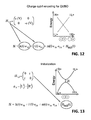
- FIG. 12 illustrates exemplary Hamiltonian encoding of the charge qubit single-qubit terms for a quadratic unconstrained binary optimization (QUBO) problem, where Coulombic coupling is used to establish the m term in the Hamiltonian ( FIG. 16 ).
- QUBO quadratic unconstrained binary optimization
- FIG. 13 illustrates exemplary Hamiltonian encoding of the charge qubit single-qubit terms for initialization of a quadratic unconstrained binary optimization (QUBO) problem.
- QUBO quadratic unconstrained binary optimization
- FIG. 14 illustrates an evolution process pertaining to a quantum computing apparatus, where two evolutions are illustrated showing the advantage of independent control over the h and gamma (e.g., t or tunnel coupling) terms in the Hamiltonian.
- gamma e.g., t or tunnel coupling
- QUBO quadratic unconstrained binary optimization
- FIG. 17 illustrates readout and layout for coupling without a bar for an exemplary qubit in a linear array lay-out.
- FIG. 19 depicts the initialization Hamiltonian for QUBO and one approach, schematically (right image) to generating the necessary gradient field (i.e., local inductor) of an exemplary qubit.
- FIG. 20 illustrates evolution from a single qubit to a coupled qubit.
- FIG. 21 is a flow diagram illustrating an exemplary methodology for obtaining a solution to an optimization problem provided to a quantum computing apparatus.
- the term “or” is intended to mean an inclusive “or” rather than an exclusive “or.” That is, unless specified otherwise, or clear from the context, the phrase “X employs A or B” is intended to mean any of the natural inclusive permutations. That is, the phrase “X employs A or B” is satisfied by any of the following instances: X employs A; X employs B; or X employs both A and B.
- the articles “a” and “an” as used in this application and the appended claims should generally be construed to mean “one or more” unless specified otherwise or clear from the context to be directed to a singular form.
- the term “exemplary” is intended to mean serving as an illustration or example of something, and is not intended to indicate a preference.
- a qubit formed in a semiconductor material is described herein (semiconductor qubit), wherein the qubit is configured for utilization in an adiabatic quantum computing apparatus.
- the qubit can be initialized to reside in the ground energy state, and a tunnel coupling parameter can be relatively slowly changed to cause the qubit to remain in the ground state. Subsequently, a value of the semiconductor qubit can be read, wherein a solution to an optimization problem is based upon the value.
- the semiconductor qubit can be initialized to have a state that corresponds to a superposition of
- the quantum computing apparatus 100 can be operated in a refrigerator.
- the quantum computing apparatus 100 includes a semiconductor material 102 , which can be any suitable semiconductor material, including but not limited to silicon (Si), gallium arsenide (GaAs), etc.
- a grid (a plurality) of semiconductor adiabatic qubits 104 is formed in the semiconductor material 102 .
- the semiconductor qubits 104 can be initialized based upon a Hamiltonian that represents an optimization problem for which a solution is desired.
- the semiconductor qubits 104 may be charge qubits, wherein such charge qubits can be double quantum dot (DQD) qubits.
- DQD double quantum dot
- the qubits 104 are DQDs
- 1> states can be defined as left or right occupation of the DQD.
- the DQD is a lateral electrostatically gated structure that can have a total of one electron or many electrons for which a single electron instability (left or right occupation) is exploited.
- the semiconductor qubits 104 can represent values as a function of spin direction of electrons.
- the quantum computing apparatus 100 may also include or be associated with at least one voltage source 106 that can output a voltage that is directed to at least one qubit in the plurality of semiconductor qubits 104 .
- the voltage output by the voltage source 106 can be configured to set a value for a tunable parameter of the semiconductor qubit.
- each qubit in the plurality of semiconductor qubits 104 can have a parameter associated therewith, wherein a state of a respective qubit can be biased as a function of a value of the parameter.
- the voltage source 106 can output a signal that causes at least one qubit in the semiconductor qubits 104 to be biased towards a value of that can be tuned and/or programmed, such that the at least one qubit is biased towards a
- a first qubit in the semiconductor qubits 104 can be (Coulombically) coupled to a second qubit in the semiconductor qubits 104 , wherein a degree of such coupling is tunable.
- the voltage source 106 can output a voltage signal that is directed towards at least one qubit in the semiconductor qubits 104 , wherein the voltage signal controls a degree of (Coulombic) coupling between the at least one qubit and a neighboring qubit in the plurality of semiconductor qubits 104 .
- such coupling can be fixed (rather than tunable).
- the plurality of semiconductor qubits 104 can have a parameter associated therewith that can be controlled to cause the plurality of semiconductor qubits 104 to have a quantum mechanical superposition of
- the voltage source 106 can output a voltage signal that causes at least one qubit in the plurality of semiconductor qubits 104 to have a state that corresponds to the superposition of
- the voltage source 106 can output a voltage signal that causes the plurality of semiconductor qubits 104 to simultaneously have states corresponding to the superposition of
- the magnitude of this parameter can be tuned from being much larger than other terms in a problem Hamiltonian to being much smaller than other terms in the problem Hamiltonian.
- the quantum computing apparatus 100 further includes readout electronics 108 that can be configured to ascertain values of qubits in the plurality of semiconductor qubits 104 .
- the readout electronics 108 include a scanning electron microscope (SEM), which can generate a SEM image. The read-out is done using a small constriction near the DQD, a quantum point contact (QPC). The conductance is sensitive to the position of the electron in the DQD, which indicates the state of the qubit. Values can be manually identified by way of inspecting the qubits 104 with the SEM. Other techniques for reading values of the qubits 104 are described below.
- the quantum computing apparatus 100 can be configured to utilize an adiabatic quantum annealing technique in connection with solving an optimization problem.
- the voltage source 106 is configured to output voltage signals corresponding to desired parameter values for Eq. (1).
- the voltage source 106 can output voltage signals that bias particular qubits to particular states, can optionally output voltage signals that define a degree of coupling between any neighboring qubits, and can further output voltage signals that cause certain qubits to have states associated with the superposition of the
- the voltage source 106 is configured to emit voltage signals that initialize the plurality of semiconductor qubits 104 for the optimization problem that is desirably solved. Subsequently, the voltage source 106 can output voltage signals that reduce the coupling between qubits in the plurality of qubits 104 . As the coupling is reduced, the qubits settle to states that can be read by the readout electronics 108 , wherein the final states of the qubits 104 is indicative of the solution to the optimization problem.
- the coupling between qubits in the plurality of semiconductor qubits 104 can be fixed (not tunable).
- the plurality of semiconductor qubits 104 can be initially placed in a non-ground state by way of application of an external energy. Such energy can be slowly reduced until the ground state is reached, and values of the qubits 104 can subsequently be read by the readout electronics 108 .
- an exemplary layout 200 of electrodes used to form a DQD is shown.
- the electrodes include: an L electrode, an LP electrode, a CP electrode, an RP electrode, an R electrode, and a T electrode.
- the exemplary DQD is also shown as including two electrodes (on the far left and far right) that form the QPCs for charge sensing.
- Voltage on electrodes LP and RP can control detuning and the magnitude of ⁇ .
- Voltage on the electrode CP (relative to T) can control the magnitude of ⁇ .
- Voltage on CP relative to T can be used to enhance or decrease tunnel coupling of the DQD with respect to a neighboring qubit, and can thus be varied in time.
- FIG. 2 further includes a cross-sectional view 202 of the DQD.
- the DQD can include an aluminum electrode (top gate) layered on a relatively thin insulating material (SiO 2 ).
- the aluminum electrode can be positively charged, thus attracting electrons in the Si substrate to the insulating material.
- the DQD is thereby formed on the upper portion of Si.
- the magnitude of the detuning can be selected as being between approximately ⁇ 10,000 ueV and approximately 10,000 ueV (e.g., wherein “approximately” is intended to refer to a range within 10% of the specified value).
- a limit of detuning can be set by a quantum dot energy scale called Coulomb blockade, which is the change in chemical potential sufficient to change the total electron occupation on a dot.
- the Coulomb blockade energy for small dots can be approximately 10 meV.
- the detuning range can be limited to between approximately ⁇ 240 ueV to 240 ueV. Larger ranges are possible for both parameters.
- An energy range for an exemplary charge qubit can correspond to temperatures of approximately 3K.
- At least the plurality of qubits 104 of the quantum computing apparatus 100 can, therefore, individually be operated in a refrigerator that can obtain as low a temperature as possible, while supporting electronics input/output, including thermal load of the electronics staged at the cold stage. Additional detail pertaining to layout and electronic staging is set forth below. Further, additional detail about relevant temperature and noise processes is also discussed below. It can be noted that alternative approaches to a cold finger design of dilution refrigerators is also possible, and may assist in maintaining low electron temperatures. For example, immersion of a quantum processor chip in an He3/He4 mixture can produce improved thermal contact to both the substrate and metal connections.
- a first view 300 shown in FIG. 3 depicts a schematic coupling between two neighboring qubits as a function of Coulomb repulsion.
- a charge qubit is an effective electric dipole
- the state of one neighbor qubit affects the relative energies of the left or right state of its neighbors.
- the dot represents the electron position.
- the three cases shown represent three different energy configurations, the top most being the lowest energy (i.e., lowest repulsion). Such interaction can be mediated through direct proximity or, alternatively, a coupling capacitance.
- a second view 302 in FIG. 3 also illustrates capacitive coupling between DQDs, wherein such coupling is fixed.
- FIG. 4 depicts an exemplary approach where coupling between neighboring DQDs can be made tunable.
- an electrode can be provided with a signal that causes the electron density in an unconnected channel between the two qubits to alter from being a metallic bar to insulting and therefore removing the coupling.
- Coupling energies similar to the fixed case can be achieved. Such energies correspond to temperatures of approximately 3 Kelvin. Achievable energies are a function of the limits in fabrication.
- Proximity of the quantum dots to one another and the charge qubits proximity to coupling electrodes determines the range of energies available in the Hamiltonian. Scanning tunneling microscope (STM) assisted fabrication techniques can be utilized to locate capacitor couplers with atomic precision, thereby allowing for much higher coupling energies to be achieved.
- STM scanning tunneling microscope
- Each qubit state is measured at the end of the algorithm in the Z eigenbasis (i.e.,
- a neighboring charge sensor i.e., QPC or SET
- Such conductance is sensitive to the local electrostatic environment and can sense a single electron change in occupation. Accordingly, the measurement technique described herein measures
- the arbitrary measurement time is a positive feature of using the ground state in the adiabatic quantum optimization approach compared to non-adiabatic qubit approaches.
- an alternative measurement technique can be to measure current directly through a charge qubit.
- a high-frequency pulse can be applied to a gate that would shift the double quantum dot into a resonant condition (that passes current) only for the
- FIG. 5 depicts an exemplary measurement technique for a silicon metal oxide semiconductor (MOS) quantum dot.
- MOS silicon metal oxide semiconductor
- FIG. 5 depicts a scanning electron microscope image 500 of a first level of electrodes, as well as a cross-section of the layers of the nanostructure 502 .
- Current through the charge center (gate E) introduces an electron, and a charge sensor can be positioned to detect such electron as shown in FIG. 5 .
- FIG. 6 includes a graph 600 that depicts current through a quantum dot and through a neighboring charge sensor. As shown in FIG. 6 , jumps in the charge sensor current correspond to changes in the electron occupation in the dot. This can be used to distinguish between
- the final state is a product state in the Z eigenbasis. That is, each qubit is either a
- Measurement of non-Z eigenbasis states can be accomplished through a non-adiabatic pulse and a single shot readout. For improved signal to noise in a charge qubit, multiple single shots can be performed, assuming that the qubit will relax back to the ground state sufficiently long after the non-adiabatic pulse has occurred.
- the semiconductor qubits 104 of the quantum computing apparatus 100 can be operated in a refrigerator.
- the adiabatic computation can rely on energy gap protection to preserve the ground state, wherein the energy gap corresponding to the semiconductor qubits is larger than that associated with conventional superconductor qubits.
- Environmental sources of energy greater than the gap that couple with the charge qubit may cause errors.
- the computation can be implemented and the qubits can be operated in a refrigerator, such as a dilution refrigerator, to reduce thermal energies below the gap energies near the charge qubit.
- Dilution refrigerators can achieve base temperatures of on the order of 0.01K, and other refrigeration systems can achieve even lower temperatures. The base temperature establishes roughly the temperature of the semiconductor crystal and the phonon population in the crystal.
- the electrons may become weakly coupled to the phonon bath and electrons in quantum dots are effectively at 0K, assuming that the quantum dots are very weakly coupled to their electrical leads (e.g., through a large tunnel barrier) and have an excited state spectrum with a large energy gap between the ground and next excited state.
- quantum dots or single donors
- Such conditions are met for few electron quantum dots (or single donors), which are charge-sensed and have either relative large tunnel coupling (>>8 ueV) or large detuning (also greater than approximately 8 ueV).
- Errors that may be of concern during evolution are those related to Landau-Zener transitions due to too rapid evolution through small gap regions and excitations from the ground state to any higher-excited state.
- the optimal evolution speed and path represents a challenge because it is dominated by the smallest gap region.
- Knowledge of the smallest gap is related to the knowledge of the solution to the problem represented by the Hamiltonian.
- a potential advantage of the semiconductor qubits is that the evolution path is made flexible through the ability to change the detuning (both negative and positive symmetrically), as well as independently tune the tunnel coupling.
- the independent tunability of such parameters differentiates the semiconductor qubits 104 from conventional qubits, and mitigates errors that may be caused by Landau-Zener transitions.
- Errors caused by excitations may occur through interactions with phonons or more complex interactions with fluctuating charge defects. Plasmons and other excitations also cannot be ruled out as potential sources of excitations. Silicon may be particularly well-suited for forming the qubits 104 , because silicon does not have as strong a piezoelectric component, and the interaction times can be slow (depending on the gap energy). That is, the probability of error can be small if the evolution through the smallest energy gap region is rapid compared to the phonon interaction time.
- FIG. 7 includes graphs 802 and 804 that depict a theoretical calculation of phonon lifetimes as a function of energy. It can be noted that at least three qubit design methods can be pursued to suppress phonon interactions with the charge qubit.
- the material choice can significantly alter the interactions of the phonons with the charge qubits, as indicated in graph 802 . Silicon, for example, has a more significant decay in interaction times than gallium arsenide and other piezoelectric materials.
- the cutoff frequency of the phonon energy interaction with the charge qubit is related to the size of the double quantum dot. That is, wavelengths much shorter than the size of the charge qubit do not couple well with the charge qubit.
- the size of the qubit can be fabricated, therefore, to suppress higher energy phonon interactions and allow the charge qubits to probe smaller gap problems.
- the phonon population may also be significantly suppressed by building the charge qubits on silicon that has been etched to make a phonon bandgap in wavelengths ( energies) for which the charge qubit is potentially most sensitive.
- Charge fluctuations from defects in the material also can couple to a charge qubit and alternately produce excitations.
- An exemplary nano-fabrication process flow has been developed for MOS charge qubits intended to minimize the effects in the system. Charge defects may further be avoided by building the charge qubits in enhance mode SiGe/sSi gate stacks.
- STM-assisted fabrication can be employed to tune the size of the double quantum dot, electron number, and strength of coupling with atomic precision. STM-assisted fabrication has been shown to produce devices that have been measured with over an order of magnitude improvement in 1/f noise, which is often associated with charge traps/fluctuators.
- FIG. 8 depicts an exemplary layout 800 for donor-based charge qubits.
- the fabrication technique used for these donor based qubit realizations is based on STM assisted fabrication. This technique of fabrication achieves atomic precision and can be used to lay-out charge qubits with relatively precise control over proximity of gates and quantum dots for relatively large ranges of energies. Additionally, STM-assisted fabrication can be used to produce relatively high uniformity, thus resulting in relatively high yield. Uniformity and yield are presently two significant challenges for the leading adiabatic qubit technology, superconducting flux qubits.
- Non-uniformity introduces shifts in the Hamiltonian values h and J that lead to the computer solving the incorrect problem, which becomes a challenging problem to debug or an extremely costly and time consuming process of characterizing and tuning every qubit.
- the charge qubit has a natural relaxation mechanism that can produce a self-correcting effect. That is, the extra energy in an excited state will entropically be driven into the surrounding environmental bath (for open system Free energy reasons). Therefore, if an excitation occurs due to either Landau-Zener or other processes, the charge qubits will have, in some cases, a non-negligible probability to release the energy and relax to the ground state, thus recovering the solution state.
- Phonon cavities that may allow relatively long phonon lifetimes, can be used, such that many body-related phonon relaxation events may occur. In other words, for large systems, there is reason to believe that the lowest energy excited states are those that require several bits to flip, and such states may be frustrated from relaxation. Self-correcting paths, however, can be enhanced in phonon cavities.
- a combination of phonon bandgap engineering and phonon density of states enhancement can be employed to engineer relaxation mechanisms towards self-correction.
- adiabatic quantum computing may require a broader hardware gate set for implementation.
- ZX and XX interaction are desirable. Accordingly, a ZX interaction can be obtained through capacitively coupling the electric dipole of one qubit to the tunnel barrier of another qubit. This can be constructed through STM-assisted fabrication, which allows devices to be engineered to the limit of precision.
- exemplary interactions are depicted, including a ZZ interaction, a ⁇ ZZ interaction, an XX interaction, and an XZ interaction, wherein the interactions are a function of location of the tunnel coupling between DQDs.
- Gap sizes of a small multi-qubit system will be order of the coupling strength (e.g., ⁇ 100 ueV for non STM based structures), which implies that relatively rapid single qubit adiabatic evolutions are possible (e.g. much larger than 1 GHz). It can be noted that quantum algorithms are pursued because for certain calculations they are polynomial or exponentially more efficient than the best classical algorithms available. This implies that the speed of operation of single qubits does not need to be faster than classical transistor speeds in order to achieve extraordinary speed-ups.
- FIG. 4 and FIG. 10 depict exemplary layouts 400 and 1000 of electrodes corresponding to a pair of qubits.
- FIG. 11 depicts an exemplary design for controlling voltages on gates including tunnel coupling corresponding to qubits in the plurality of semiconductor qubits 104 (as well as electronics for characterization and tuning and electronics for obtaining a measurement signal).
- Cryogenic CMOS can be included on the same quantum process chip for MUX and DEMUX. This is most readily achieved when implementing the qubit with the silicon material system.
- Voltages on electrodes that are not directly controlled during the computation i.e., the tunnel barrier electrodes that control the gamma parameter in the Hamiltonian
- the electrical input/output complexity is considerably less in the adiabatic quantum annealing approach compared to many other proposed quantum computing approaches.
- a single parameter in the Hamiltonian is slowly modified, and the magnitude and rate of change can be the same for every qubit. More flexibility can be beneficial, however, the minimum requirement for the hardware is a simple global parameter change. Electrically, this can represent only a single voltage changing in time and the change in time will be relatively slow.
- compensating voltages can be applied to more than one gate, wherein the compensating voltages can be tied to a single global voltage combined with programmed voltage dividers for each qubit (although other approaches are contemplated). Additionally, gap size may shrink as the problem size increases.
- each qubit may have two eigenstates (binary answers) associated therewith, which are non-degenerate in nature.
- the qubit can start in a superposition between the two eigenstates, wherein the superposition is the ground state of an initial Hamiltonian.
- H init initial can be slowly reduced and/or H problem can be slowly increased.
- H final H problem H init .
- the state of each qubit is measured, wherein in some embodiments, the state must be measured prior to information being lost.
- FIG. 12 an exemplary charge qubit encoding for a QUBO problem is illustrated. Modulation of k and l, circled in FIG. 12 , can be accomplished with voltages on gates (e.g., as output by the control voltage source 106 ). Turning to FIG. 13 , initialization pertaining to the qubit is depicted.
- spin degree of freedom for adiabatic quantum computing is an alternative to a charge qubit. Such approach has several advantages and disadvantages relative to the charge qubit.
- Advantages include 1) weaker coupling to environmental noise; 2) better temporal coherence for system that include a relatively small number of qubits (especially in the isotope enriched systems, such as 28 Si); 3) an existing experimentally-demonstrated path towards higher fidelity non-adiabatic operations that can be used for measurement outside of the Z eigenbasis; 4) sufficient temporal coherence to potentially more easily examined time-resolved tomography of the adiabatic state of each individual qubit; and 5) slower dissipative relaxation mechanisms.
- Disadvantages of such approach relative to charge qubits include: 1) the uncertain path towards achieving a large tunnel couple bandgap; 2) slower evolution times because of small bandgap; 3) challenging initialization state to produce; 4) a smaller range of the de-tuning or trade-off for faster energy relaxation mechanisms; and 5) increased difficulty of fabrication.
- the alternate qubit subspace is depicted.
- the encoding shown in the algorithm of FIG. 15 uses the ground state instead of a metastable subspace, such that the k and l range is more flexible.
- FIG. 16 depicts nearest neighbor qubit interaction with such a qubit.
- m is positive and can be modulated using voltage on a barrier gate.
- Interaction magnitude is anecdotally observed to be approximately 0.1 J and coefficients can be tuned to produce Z 1 and Z 2 .
- FIG. 16 further includes a graph 1700 that illustrates energy associated with two qubits interacting.
- FIG. 17 illustrates readout and layout for coupling without a bar
- FIG. 18 depicts S/T0 qubit encoding.
- modulation of k and l can be accomplished with J(V), where ⁇ J can be produced with certain parameters of B z , V and dot size.
- J can range from ueV to meV (or more).
- the magnitude of the gradient may determine the minimum gap.
- FIGS. 21 and 22 illustrate exemplary methodologies relating to quantum computing. While the methodologies are shown and described as being a series of acts that are performed in a sequence, it is to be understood and appreciated that the methodologies are not limited by the order of the sequence. For example, some acts can occur in a different order than what is described herein. In addition, an act can occur concurrently with another act. Further, in some instances, not all acts may be required to implement a methodology described herein.
- the methodology 2100 starts at 2102 , and at 2104 , a plurality of semiconductor adiabatic qubits are configured in accordance with a Hamiltonian.
- the Hamiltonian can represent an optimization problem that is desirably solved by way of a quantum computing apparatus.
- the plurality of semiconductor adiabatic qubits are retained in a ground state including cases for which noise produced an excitation (i.e., error) but was self-corrected through relaxation mechanisms inherent to the charge qubit. That is, as noted above, the qubits can be initialized in the ground state, such that there is tunnel coupling and values of the qubits are superpositions of
- the tunnel coupling barrier can be raised slowly (e.g., thus inhibiting tunnel coupling), thereby causing the qubits to have states that are collectively indicative of a solution to the optimization problem.
- respective values in the plurality of semiconductor adiabatic qubits are read, wherein such values are indicative of the solution to the optimization problem.
- the methodology 2100 completes at 2110 .
Landscapes
- Engineering & Computer Science (AREA)
- Physics & Mathematics (AREA)
- Power Engineering (AREA)
- Microelectronics & Electronic Packaging (AREA)
- General Physics & Mathematics (AREA)
- Theoretical Computer Science (AREA)
- Condensed Matter Physics & Semiconductors (AREA)
- Computer Hardware Design (AREA)
- Ceramic Engineering (AREA)
- Mathematical Physics (AREA)
- Computing Systems (AREA)
- Chemical & Material Sciences (AREA)
- General Engineering & Computer Science (AREA)
- Evolutionary Computation (AREA)
- Data Mining & Analysis (AREA)
- Nanotechnology (AREA)
- Artificial Intelligence (AREA)
- Software Systems (AREA)
- Computational Mathematics (AREA)
- Mathematical Optimization (AREA)
- Pure & Applied Mathematics (AREA)
- Mathematical Analysis (AREA)
- Crystallography & Structural Chemistry (AREA)
- Computational Linguistics (AREA)
- Superconductor Devices And Manufacturing Methods Thereof (AREA)
Abstract
Description
H problem H init=−Σi h iσiz+Σi,j>1 K ijσjz−Γ(t)Σiσix (1)
-
- For the charge qubit, σx and σz are Pauli operators for pseudo spin bases of the |L> and |R> states. The parameters h and Γ can be controlled by the voltage source 106 (e.g., by changing voltages associated therewith).
Claims (20)
Priority Applications (1)
| Application Number | Priority Date | Filing Date | Title |
|---|---|---|---|
| US14/054,659 US9530873B1 (en) | 2013-01-28 | 2013-10-15 | Semiconductor adiabatic qubits |
Applications Claiming Priority (2)
| Application Number | Priority Date | Filing Date | Title |
|---|---|---|---|
| US201361757609P | 2013-01-28 | 2013-01-28 | |
| US14/054,659 US9530873B1 (en) | 2013-01-28 | 2013-10-15 | Semiconductor adiabatic qubits |
Publications (1)
| Publication Number | Publication Date |
|---|---|
| US9530873B1 true US9530873B1 (en) | 2016-12-27 |
Family
ID=57590152
Family Applications (1)
| Application Number | Title | Priority Date | Filing Date |
|---|---|---|---|
| US14/054,659 Active 2034-08-02 US9530873B1 (en) | 2013-01-28 | 2013-10-15 | Semiconductor adiabatic qubits |
Country Status (1)
| Country | Link |
|---|---|
| US (1) | US9530873B1 (en) |
Cited By (19)
| Publication number | Priority date | Publication date | Assignee | Title |
|---|---|---|---|---|
| US20180226451A1 (en) * | 2015-08-05 | 2018-08-09 | Newsouth Innovations Pty Limited | Advanced processing apparatus comprising a plurality of quantum processing elements |
| US10482388B1 (en) * | 2018-06-29 | 2019-11-19 | National Technology & Engineering Solutions Of Sandia, Llc | Spin-orbit qubit using quantum dots |
| US10592216B1 (en) | 2017-11-15 | 2020-03-17 | Amazon Technologies, Inc. | Development environment for programming quantum computing resources |
| CN111464154A (en) * | 2019-01-22 | 2020-07-28 | 华为技术有限公司 | Control pulse calculation method and device |
| US10817337B1 (en) | 2017-11-15 | 2020-10-27 | Amazon Technologies, Inc. | Cloud-based access to quantum computing resources |
| US10885678B2 (en) * | 2017-09-29 | 2021-01-05 | International Business Machines Corporation | Facilitating quantum tomography |
| WO2021168019A1 (en) * | 2020-02-18 | 2021-08-26 | The University Of Chicago | Universal fast-flux control of low-frequency qubits |
| US11170137B1 (en) | 2017-11-15 | 2021-11-09 | Amazon Technologies, Inc. | Cloud-based simulation of quantum computing resources |
| US11270220B1 (en) | 2017-11-15 | 2022-03-08 | Amazon Technologies, Inc. | Service for managing quantum computing resources |
| US20220083894A1 (en) * | 2017-09-29 | 2022-03-17 | International Business Machines Corporation | Debugging quantum circuits by circuit rewriting |
| EP3971982A1 (en) * | 2020-09-21 | 2022-03-23 | Commissariat à l'Energie Atomique et aux Energies Alternatives | Bifunctional routing chip and method for manufacturing same |
| US20220214991A1 (en) * | 2014-03-21 | 2022-07-07 | Google Llc | Chips including classical and quantum computing processors |
| US11468180B2 (en) * | 2020-03-31 | 2022-10-11 | Fujitsu Limited | Data privacy protection on cloud-based optimization systems |
| EP4075153A1 (en) * | 2021-04-12 | 2022-10-19 | Qdevil ApS | Low temperature oscilloscope |
| US11605016B2 (en) | 2019-11-27 | 2023-03-14 | Amazon Technologies, Inc. | Quantum computing service supporting local execution of hybrid algorithms |
| US11605033B2 (en) | 2019-11-27 | 2023-03-14 | Amazon Technologies, Inc. | Quantum computing task translation supporting multiple quantum computing technologies |
| US11620561B2 (en) | 2018-05-30 | 2023-04-04 | Mark A. Novotny | Method and system for a quantum oracle to obtain the number of quantum ground states |
| US11704715B2 (en) | 2019-11-27 | 2023-07-18 | Amazon Technologies, Inc. | Quantum computing service supporting multiple quantum computing technologies |
| US11907092B2 (en) | 2021-11-12 | 2024-02-20 | Amazon Technologies, Inc. | Quantum computing monitoring system |
Citations (5)
| Publication number | Priority date | Publication date | Assignee | Title |
|---|---|---|---|---|
| US20050224784A1 (en) * | 2004-03-29 | 2005-10-13 | Amin Mohammad H S | Adiabatic quantum computation with superconducting qubits |
| US20070180586A1 (en) * | 2006-01-27 | 2007-08-02 | Amin Mohammad H | Methods of adiabatic quantum computation |
| US20100241780A1 (en) * | 2005-09-30 | 2010-09-23 | Friesen Mark G | Spin-bus for information transfer in quantum computing |
| US20110054876A1 (en) * | 2007-04-05 | 2011-03-03 | Jacob Daniel Biamonte | Physical realizations of a universal adiabatic quantum computer |
| US20110121895A1 (en) * | 2008-02-11 | 2011-05-26 | Andrea Morello | Control and readout of electron or hole spin |
-
2013
- 2013-10-15 US US14/054,659 patent/US9530873B1/en active Active
Patent Citations (5)
| Publication number | Priority date | Publication date | Assignee | Title |
|---|---|---|---|---|
| US20050224784A1 (en) * | 2004-03-29 | 2005-10-13 | Amin Mohammad H S | Adiabatic quantum computation with superconducting qubits |
| US20100241780A1 (en) * | 2005-09-30 | 2010-09-23 | Friesen Mark G | Spin-bus for information transfer in quantum computing |
| US20070180586A1 (en) * | 2006-01-27 | 2007-08-02 | Amin Mohammad H | Methods of adiabatic quantum computation |
| US20110054876A1 (en) * | 2007-04-05 | 2011-03-03 | Jacob Daniel Biamonte | Physical realizations of a universal adiabatic quantum computer |
| US20110121895A1 (en) * | 2008-02-11 | 2011-05-26 | Andrea Morello | Control and readout of electron or hole spin |
Non-Patent Citations (17)
| Title |
|---|
| Burkard, G. "Theory of solid state quantum information processing." arXiv preprint cond-mat/0409626 (2004). 57 pages. * |
| Farhi, et al., "Quantum Computation by Adiabatic Evolution", MIT CTP # 2936, Jan. 28, 2000, pp. 1-24. |
| Fuechsle, et al., "Spectroscopy of Few-Electron Single-Crystal Silicon Quantum Dots", Nature Technology, 2010, pp. 1-4. |
| Fuhrer, A. et al. "Few electron double quantum dots in InAs/InP nanowire heterostructures." Nano letters 7.2 (2007): 243-246. Web Publication: Dec. 24, 2006. DOI: 10.1021/nI061913f. * |
| Gupta, N. "Numerical studies of transport and spin-orbit exchange in InAs nanowires." Thesis, University of Waterloo. (2013). 74 pages. * |
| Johnson, et al., "Quantum Annealing with Manufactured Spins", Nature, vol. 473, May 12, 2011, pp. 194-198. |
| Ramsay, A.J. "A review of the coherent optical control of the exciton and spin states of semiconductor quantum dots." Semiconductor Science and Technology 25.10 (2010): 103001. 23 pages. DOI:10.1088/0268-1242/25/10/103001. * |
| Rohling, N. et al. "Universal quantum computing with spin and valley states." New Journal of Physics 14.8 (Aug. 2012): 083008. 19 pages. doi:10.1088/1367-2630/14/8/083008. * |
| Santoro, et al., "Theory of QUantum Annealing of an Ising Spin Glass", Science, vol. 29, Mar. 2002, pp. 2427-2430. |
| Storcz, M.J. "Decoherence, control, and encoding of coupled solid-state quantum bits." PhD diss., Ludwig-Maximilians-Universitat, Munchen. (Aug. 2005). 273 pages. * |
| Taylor, et al., "Fault-tolerant Architecture for Quantum Computation Using Electrically Controlled Semiconductor Spins", Nature Physics, vol. 1, Dec. 2005, pp. 177-183. |
| Taylor, J.M. "Hyperfine interactions and quantum information processing in quantum dots." PhD diss., Harvard University Cambridge, Massachusetts. (2006). 309 pages. * |
| van der Wiel, et al., "Electron Transport Through Double Quantum Dots", Review of Modern Physics, vol. 75, Jan. 2003, pp. 1-22. |
| van Weperen, et al., "Charge-State Conditional Operation of a Spin Qubit", Physical Review Letters, Jul. 15, 2011, pp. 1-4. |
| Wilhelm, F.K. et al. "Superconducting Qubits II: Decoherence." Manipulating Quantum Coherence in Solid State Systems. NATO Science Series II: Mathematics, Physics and Chemistry vol. 244, 2007, pp. 195-232. * |
| Zgak, R.A, et al. (2009). "Quantum computing with electron spins in quantum dots." 61 pages. arXiv preprint arXiv:0906.4045. * |
| Żġak, R.A, et al. (2009). "Quantum computing with electron spins in quantum dots." 61 pages. arXiv preprint arXiv:0906.4045. * |
Cited By (26)
| Publication number | Priority date | Publication date | Assignee | Title |
|---|---|---|---|---|
| US20220214991A1 (en) * | 2014-03-21 | 2022-07-07 | Google Llc | Chips including classical and quantum computing processors |
| US10692924B2 (en) * | 2015-08-05 | 2020-06-23 | Newsouth Innovations Pty Limited | Advanced processing apparatus comprising a plurality of quantum processing elements |
| US20180226451A1 (en) * | 2015-08-05 | 2018-08-09 | Newsouth Innovations Pty Limited | Advanced processing apparatus comprising a plurality of quantum processing elements |
| US10885678B2 (en) * | 2017-09-29 | 2021-01-05 | International Business Machines Corporation | Facilitating quantum tomography |
| US11809962B2 (en) * | 2017-09-29 | 2023-11-07 | International Business Machines Corporation | Debugging quantum circuits by circuit rewriting |
| US20220083894A1 (en) * | 2017-09-29 | 2022-03-17 | International Business Machines Corporation | Debugging quantum circuits by circuit rewriting |
| US10817337B1 (en) | 2017-11-15 | 2020-10-27 | Amazon Technologies, Inc. | Cloud-based access to quantum computing resources |
| US10592216B1 (en) | 2017-11-15 | 2020-03-17 | Amazon Technologies, Inc. | Development environment for programming quantum computing resources |
| US11170137B1 (en) | 2017-11-15 | 2021-11-09 | Amazon Technologies, Inc. | Cloud-based simulation of quantum computing resources |
| US11270220B1 (en) | 2017-11-15 | 2022-03-08 | Amazon Technologies, Inc. | Service for managing quantum computing resources |
| US11775855B2 (en) | 2017-11-15 | 2023-10-03 | Amazon Technologies, Inc. | Service for managing quantum computing resources |
| US11620561B2 (en) | 2018-05-30 | 2023-04-04 | Mark A. Novotny | Method and system for a quantum oracle to obtain the number of quantum ground states |
| US10482388B1 (en) * | 2018-06-29 | 2019-11-19 | National Technology & Engineering Solutions Of Sandia, Llc | Spin-orbit qubit using quantum dots |
| CN111464154A (en) * | 2019-01-22 | 2020-07-28 | 华为技术有限公司 | Control pulse calculation method and device |
| CN111464154B (en) * | 2019-01-22 | 2022-04-22 | 华为技术有限公司 | Control pulse calculation method and device |
| US11605016B2 (en) | 2019-11-27 | 2023-03-14 | Amazon Technologies, Inc. | Quantum computing service supporting local execution of hybrid algorithms |
| US11605033B2 (en) | 2019-11-27 | 2023-03-14 | Amazon Technologies, Inc. | Quantum computing task translation supporting multiple quantum computing technologies |
| US11704715B2 (en) | 2019-11-27 | 2023-07-18 | Amazon Technologies, Inc. | Quantum computing service supporting multiple quantum computing technologies |
| WO2021168019A1 (en) * | 2020-02-18 | 2021-08-26 | The University Of Chicago | Universal fast-flux control of low-frequency qubits |
| US11468180B2 (en) * | 2020-03-31 | 2022-10-11 | Fujitsu Limited | Data privacy protection on cloud-based optimization systems |
| FR3114444A1 (en) * | 2020-09-21 | 2022-03-25 | Commissariat A L'energie Atomique Et Aux Energies Alternatives | Bifunctionally routed chip and associated manufacturing method |
| EP3971982A1 (en) * | 2020-09-21 | 2022-03-23 | Commissariat à l'Energie Atomique et aux Energies Alternatives | Bifunctional routing chip and method for manufacturing same |
| US11823997B2 (en) | 2020-09-21 | 2023-11-21 | Commissariat A L'energie Atomique Et Aux Energies Alternatives | Chip with bifunctional routing and associated method of manufacturing |
| EP4075153A1 (en) * | 2021-04-12 | 2022-10-19 | Qdevil ApS | Low temperature oscilloscope |
| WO2022218844A1 (en) | 2021-04-12 | 2022-10-20 | Qdevil Aps | Low temperature oscilloscope |
| US11907092B2 (en) | 2021-11-12 | 2024-02-20 | Amazon Technologies, Inc. | Quantum computing monitoring system |
Similar Documents
| Publication | Publication Date | Title |
|---|---|---|
| US9530873B1 (en) | Semiconductor adiabatic qubits | |
| US20210342730A1 (en) | System and method of quantum enhanced accelerated neural network training | |
| US10255556B2 (en) | Apparatus and method for quantum processing | |
| US6635898B2 (en) | Quantum computer | |
| US10482388B1 (en) | Spin-orbit qubit using quantum dots | |
| JP4819994B2 (en) | Quantum computer | |
| US9886668B2 (en) | Advanced processing apparatus | |
| Kane | A silicon-based nuclear spin quantum computer | |
| US10657456B1 (en) | Quantum computing using chiral qubits | |
| US20050045872A1 (en) | Gradiometer-based flux qubit for quantum computing and method therefor | |
| US11533046B2 (en) | System and method of generating quantum unitary noise using silicon based quantum dot arrays | |
| US11910728B2 (en) | Flopping-mode electric dipole spin resonance | |
| Bhardwaj et al. | Topological materials: new quantum phases of matter | |
| JP2024512373A (en) | Qubits and quantum processing systems | |
| US20200410383A1 (en) | Nuclear spein quantum processing element and method of operation thereof | |
| Hutin et al. | MOS technology for quantum computing: recent progress and perspectives for scaling up | |
| Dumoulin-Stuyck | Design and Characterization of Quantum Sillicon-Based Devices for Semiconducting Qubit Implementation | |
| Schoenfield | Coherent Control and Spectroscopy of Valley States of Individual Electrons in Silicon Quantum Dots | |
| Ciriano Tejel | High-fidelity, compact readout of spins in silicon quantum dots | |
| TW202341018A (en) | Methods and systems for analogue quantum computing | |
| SHALAK | Docteur de l’Université de Lille | |
| Shalak | Modeling of silicon quantum bits | |
| House | Lateral Quantum Dots for Quantum Information Processing | |
| CN117949799A (en) | Method and system for measuring performance of organic spin electronic component based on gate voltage | |
| Kalra | The building blocks of a quantum computer based on donor spins in silicon |
Legal Events
| Date | Code | Title | Description |
|---|---|---|---|
| AS | Assignment |
Owner name: SANDIA CORPORATION, NEW MEXICO Free format text: ASSIGNMENT OF ASSIGNORS INTEREST;ASSIGNORS:CARROLL, MALCOLM S.;WITZEL, WAYNE;JACOBSON, NOAH TOBIAS;AND OTHERS;SIGNING DATES FROM 20150212 TO 20150807;REEL/FRAME:036318/0803 |
|
| AS | Assignment |
Owner name: U.S. DEPARTMENT OF ENERGY, DISTRICT OF COLUMBIA Free format text: CONFIRMATORY LICENSE;ASSIGNOR:SANDIA CORPORATION;REEL/FRAME:037137/0878 Effective date: 20150702 |
|
| STCF | Information on status: patent grant |
Free format text: PATENTED CASE |
|
| AS | Assignment |
Owner name: NATIONAL TECHNOLOGY & ENGINEERING SOLUTIONS OF SAN Free format text: CHANGE OF NAME;ASSIGNOR:SANDIA CORPORATION;REEL/FRAME:047052/0538 Effective date: 20170501 |
|
| MAFP | Maintenance fee payment |
Free format text: PAYMENT OF MAINTENANCE FEE, 4TH YEAR, LARGE ENTITY (ORIGINAL EVENT CODE: M1551); ENTITY STATUS OF PATENT OWNER: LARGE ENTITY Year of fee payment: 4 |