US9507584B2 - Electronic device including a memory technology device - Google Patents
Electronic device including a memory technology device Download PDFInfo
- Publication number
- US9507584B2 US9507584B2 US14/554,148 US201414554148A US9507584B2 US 9507584 B2 US9507584 B2 US 9507584B2 US 201414554148 A US201414554148 A US 201414554148A US 9507584 B2 US9507584 B2 US 9507584B2
- Authority
- US
- United States
- Prior art keywords
- ram
- kernel
- flash memory
- root
- mode
- Prior art date
- Legal status (The legal status is an assumption and is not a legal conclusion. Google has not performed a legal analysis and makes no representation as to the accuracy of the status listed.)
- Active, expires
Links
Images


Classifications
-
- G—PHYSICS
- G06—COMPUTING; CALCULATING OR COUNTING
- G06F—ELECTRIC DIGITAL DATA PROCESSING
- G06F8/00—Arrangements for software engineering
- G06F8/60—Software deployment
- G06F8/65—Updates
- G06F8/654—Updates using techniques specially adapted for alterable solid state memories, e.g. for EEPROM or flash memories
-
- G06F8/665—
-
- G—PHYSICS
- G06—COMPUTING; CALCULATING OR COUNTING
- G06F—ELECTRIC DIGITAL DATA PROCESSING
- G06F9/00—Arrangements for program control, e.g. control units
- G06F9/06—Arrangements for program control, e.g. control units using stored programs, i.e. using an internal store of processing equipment to receive or retain programs
- G06F9/44—Arrangements for executing specific programs
- G06F9/4401—Bootstrapping
- G06F9/4406—Loading of operating system
- G06F9/441—Multiboot arrangements, i.e. selecting an operating system to be loaded
Definitions
- the present disclosure relates to an electronic device including a nonvolatile storage device serving as a memory technology device (MTD).
- a nonvolatile storage device serving as a memory technology device (MTD).
- a typical electronic device that includes a nonvolatile storage device serving as the MTD may be, for example, an image forming apparatus including a random access memory (RAM) and a flash memory serving as the nonvolatile storage device.
- RAM random access memory
- flash memory serving as the nonvolatile storage device.
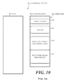
- FIG. 10 is a schematic diagram illustrating an example of a configuration of a RAM 81 and a flash memory 82 within such a typical electronic device 80 as described above.
- the electronic device 80 includes the RAM 81 and the flash memory 82 serving as a nonvolatile storage device.
- the flash memory 82 stores firmware 82 a for a Linux® system.
- the firmware 82 a includes a boot loader 82 b that is executed when the electronic device 80 is booted, a kernel 82 c to be expanded onto the RAM 81 , a root disk image 82 d for normal boot that is a root disk image serving as a compressed file of a root file system and that is used when a boot mode of the electronic device 80 is a normal boot mode, and a root disk image 82 e for update that is a root disk image used when the boot mode of the electronic device 80 is an update mode for updating the firmware 82 a on the flash memory 82 .
- the root disk image 82 d for normal boot is a file having a format that can be read by a kernel 81 c described later from the MTD via a read-only file system such as Cramfs or Squashfs.
- the root disk image 82 e for update is a file having a format that can be read by the kernel 81 c from an area of the RAM 81 under management of the kernel 81 c .
- the format that can be read by the kernel 81 c from the MTD is different from the format that can be read by the kernel 81 c from the area of the RAM 81 under the management of the kernel 81 c in terms of a mechanism of Linux®.
- the root disk image 82 d for normal boot and the root disk image 82 e for update are files having formats different from each other.
- FIG. 11 is a flowchart of an operation performed when the electronic device 80 is booted.
- FIG. 12 is a schematic diagram illustrating a configuration of the RAM 81 and the flash memory 82 employed when the boot mode of the electronic device 80 is the normal boot mode.
- FIG. 13 is a schematic diagram illustrating a configuration of the RAM 81 and the flash memory 82 employed when the boot mode of the electronic device 80 is the update mode.
- the electronic device 80 expands the boot loader 82 b on the flash memory 82 onto the RAM 81 as a boot loader 81 b (refer to FIG. 12 and FIG. 13 ) (S 91 ).
- the boot loader 81 b expands the kernel 82 c on the flash memory 82 onto the RAM 81 as the kernel 81 c (refer to FIG. 12 and FIG. 13 ) (S 92 ).
- the boot loader 81 b determines whether or not the boot mode of the electronic device 80 is the update mode (S 93 ).
- Step S 93 When determining in Step S 93 that the boot mode is not the update mode—that is, when the boot mode is the normal boot mode—the boot loader 81 b notifies the kernel 81 c that the boot mode is the normal boot mode (S 94 ).
- the kernel 81 c mounts the root disk image 82 d for normal boot on the flash memory 82 as the root file system (S 95 ). Accordingly, as illustrated in FIG. 12 , the root disk image 82 d for normal boot is read into an area of the RAM 81 not under the management of the kernel 81 c in unit of a page as the need arises.
- Step S 93 When determining in Step S 93 that the boot mode is the update mode, the boot loader 81 b notifies the kernel 81 c that the boot mode is the update mode (S 96 ).
- the kernel 81 c expands the root disk image 82 e for update on the flash memory 82 into the area of the RAM 81 under the management of the kernel 81 c as a root disk image 81 e for update (S 97 ), and then mounts the root disk image 81 e for update on the RAM 81 as the root file system (S 98 ). Accordingly, as illustrated in FIG. 13 , the root disk image 81 e for update is read into the area of the RAM 81 not under the management of the kernel 81 c in unit of the page as the need arises.
- the electronic device 80 operates in accordance with the root disk image 81 e for update on the RAM 81 , and hence can delete the firmware 82 a before update from the flash memory 82 and then write the firmware 82 a after update into the flash memory 82 .
- Step S 95 or Step S 98 the electronic device 80 finishes the operation illustrated in FIG. 11 .
- the root disk image 82 d for normal boot and the root disk image 82 e for update need to be stored in the flash memory 82 , which increases a capacity necessary for the flash memory 82 .
- the present disclosure relates to an electronic device capable of suppressing a capacity necessary for a nonvolatile storage device.
- the electronic device includes a random access memory (RAM), a nonvolatile storage device configured to act as a memory technology device (MTD), and firmware that is stored on the nonvolatile storage device.
- the firmware includes a kernel that may be expanded onto the RAM and a root disk image as a root file system.
- the kernel mounts the root disk image on the nonvolatile storage device as the root file system when a boot mode of the electronic device is a normal boot mode.
- the kernel when the boot mode is an update mode for updating the firmware on the nonvolatile storage device, may i) generate a RAM disk as an MTD in an area of the RAM not under management of the kernel, ii) expand the root disk image on the nonvolatile storage device into the RAM disk, and iii) mount the root disk image on the RAM disk as the root file system.
- FIG. 1 is a schematic diagram illustrating a block configuration of a multifunction peripheral (MFP) according to an embodiment of the present disclosure
- FIG. 2 is a schematic diagram illustrating a configuration of a RAM and a flash memory within the MFP illustrated in FIG. 1 ;
- FIG. 3 is a flowchart of an operation performed when the MFP illustrated in FIG. 1 is booted;
- FIG. 4 is a schematic diagram illustrating a configuration of the RAM and the flash memory illustrated in FIG. 2 when a boot loader has been expanded onto the RAM;
- FIG. 5 is a schematic diagram illustrating a configuration of the RAM and the flash memory illustrated in FIG. 2 when a kernel has been expanded onto the RAM;
- FIG. 6 is a schematic diagram illustrating a configuration of the RAM and the flash memory when a boot mode of the MFP is a normal boot mode
- FIG. 7 is a schematic diagram illustrating a configuration of the RAM and the flash memory illustrated in FIG. 2 when an MTDRAM disk has been generated in an area of the RAM not under management of the kernel;
- FIG. 8 is a schematic diagram illustrating a configuration of the RAM and the flash memory illustrated in FIG. 2 when a root disk image has been expanded into the MTDRAM disk;
- FIG. 9 is a schematic diagram illustrating a configuration of the RAM and the flash memory illustrated in FIG. 2 when the boot mode of the MFP is an update mode;
- FIG. 10 is a schematic diagram illustrating an example of a configuration of a RAM and a flash memory within a typical electronic device
- FIG. 11 is a flowchart of an operation performed when the typical electronic device illustrated in FIG. 10 is booted;
- FIG. 12 is a schematic diagram illustrating a configuration of the RAM and the flash memory illustrated in FIG. 10 employed when a boot mode of the typical electronic device is a normal boot mode;
- FIG. 13 is a schematic diagram illustrating a configuration of the RAM and the flash memory illustrated in FIG. 10 employed when the boot mode of the typical electronic device is an update mode.
- FIG. 1 is a schematic diagram illustrating a block configuration of an MFP 10 according to this embodiment.
- the MFP 10 includes an operation unit 11 serving as an input device such as buttons through which a user inputs various operations, a display unit 12 serving as a display device such as a liquid crystal display (LCD) that displays various kinds of information, a scanner 13 serving as a reading device that reads an image from an original, a printer 14 serving as a printing device that executes printing on a recording medium such as paper, a FAX communication unit 15 serving as a FAX device that performs FAX communications to/from an external facsimile machine (not shown) via a communication line such as a public telephone line, a network communication unit 16 serving as a network communication device that performs communications to/from an external device (not shown) via a network such as a local area network (LAN) or the Internet, and a control unit 20 that controls the entire MFP 10 .
- an operation unit 11 serving as an input device such as buttons through which a user inputs various operations
- a display unit 12 serving as a display device such as a liquid crystal display (LCD) that displays
- the control unit 20 includes a central processing unit (CPU) 21 , a read only memory (ROM) 22 that stores a program for the CPU 21 and different kinds of data, a random access memory (RAM) 23 used as a work area for the CPU 21 , and a flash memory 24 of a NAND type or a NOR type serving as an MTD.
- CPU central processing unit
- ROM read only memory
- RAM random access memory
- FIG. 2 is a schematic diagram illustrating a configuration of the RAM 23 and the flash memory 24 within the MFP 10 .
- the flash memory 24 stores firmware 24 a for a Linux® system.
- the firmware 24 a includes a boot loader 24 b that is executed when the MFP 10 is booted, a kernel 24 c to be expanded onto the RAM 23 , a root disk image 24 d serving as a compressed file of a root file system.
- the root disk image 24 d is a file having a format that can be read by the kernel 23 c described later from the MTD via a read-only file system such as Cramfs or Squashfs.
- FIG. 3 is a flowchart of an operation performed when the MFP 10 is booted.
- FIG. 4 is a schematic diagram illustrating a configuration of the RAM 23 and the flash memory 24 when a boot loader 23 b has been expanded onto the RAM 23 .
- the CPU 21 expands the boot loader 24 b on the flash memory 24 onto the RAM 23 as the boot loader 23 b as illustrated in FIG. 4 (S 31 ).
- FIG. 5 is a schematic diagram illustrating a configuration of the RAM 23 and the flash memory 24 when the kernel 23 c has been expanded onto the RAM 23 .
- Step S 31 When the process of Step S 31 is finished, the boot loader 23 b executed by the CPU 21 expands the kernel 24 c on the flash memory 24 onto the RAM 23 as the kernel 23 c as illustrated in FIG. 5 (S 32 ).
- the boot loader 23 b determines whether or not a boot mode of the MFP 10 is an update mode for updating the firmware 24 a on the flash memory 24 (S 33 ).
- Step S 33 When determining in Step S 33 that the boot mode is not the update mode, in other words, that the boot mode is a normal boot mode, the boot loader 23 b notifies the kernel 23 c that the boot mode is the normal boot mode (S 34 ).
- FIG. 6 is a schematic diagram illustrating a configuration of the RAM 23 and the flash memory 24 when the boot mode of the MFP 10 is the normal boot mode.
- the kernel 23 c executed by the CPU 21 mounts the root disk image 24 d on the flash memory 24 as a root file system (S 35 ). Accordingly, as illustrated in FIG. 6 , the root disk image 24 d is read into an area of the RAM 23 not under management of the kernel 23 c in unit of the page as the need arises.
- Step S 33 When determining in Step S 33 that the boot mode is the update mode, the boot loader 23 b notifies the kernel 23 c that the boot mode is the update mode (S 36 ).
- FIG. 7 is a schematic diagram illustrating a configuration of the RAM 23 and the flash memory 24 when an MTDRAM disk 23 a has been generated in the area of the RAM 23 not under the management of the kernel 23 c.
- the kernel 23 c When notified by the boot loader 23 b that the boot mode is the update mode, as illustrated in FIG. 7 , the kernel 23 c generates a RAM disk (hereinafter referred to as “MTDRAM disk”) 23 a serving as an MTD in the area of the RAM 23 not under the management of the kernel 23 c (S 37 ).
- MTDRAM disk a RAM disk serving as an MTD in the area of the RAM 23 not under the management of the kernel 23 c (S 37 ).
- FIG. 8 is a schematic diagram illustrating a configuration of the RAM 23 and the flash memory 24 when a root disk image 23 d has been expanded into the MTDRAM disk 23 a.
- Step S 37 the kernel 23 c expands the root disk image 24 d on the flash memory 24 into the MTDRAM disk 23 a as the root disk image 23 d as illustrated in FIG. 8 (S 38 ).
- FIG. 9 is a schematic diagram illustrating a configuration of the RAM 23 and the flash memory 24 when the boot mode of the MFP 10 is the update mode.
- the kernel 23 c mounts the root disk image 23 d on the MTDRAM disk 23 a as the root file system (S 39 ). Accordingly, as illustrated in FIG. 9 , the root disk image 23 d is read into the area of the RAM 23 not under the management of the kernel 23 c in unit of the page as the need arises. Note that, the CPU 21 operates in accordance with the root disk image 23 d on the MTDRAM disk 23 a , and hence can delete the firmware 24 a before update from the flash memory 24 and then write the firmware 24 a after update into the flash memory 24 .
- Step S 35 or Step S 39 the CPU 21 finishes the operation illustrated in FIG. 3 .
- the MFP 10 stores, in the flash memory 24 , the root disk image 24 d used in common when the boot mode is the normal boot mode and when the boot mode is the update mode, and can therefore suppress a capacity necessary for the flash memory 24 to a lower level than in a configuration in which a root disk image used when the boot mode is the normal boot mode and a root disk image used when the boot mode is the update mode are separately stored in the flash memory 24 .
- the root disk image 23 d is not expanded into the area of the RAM 23 not under the management of the kernel 23 c , which can increase the capacity of the usable area of the RAM 23 .
- the nonvolatile storage device is a flash memory in this embodiment, but may be any storage device other than the flash memory as long as the nonvolatile storage device is the MTD.
- the electronic device is an MFP in this embodiment, but may be any image forming apparatus other than the MFP, such as a copying machine or a printer, or may be any electronic device other than the image forming apparatus such as a general-purpose personal computer.
Landscapes
- Engineering & Computer Science (AREA)
- Software Systems (AREA)
- Theoretical Computer Science (AREA)
- General Engineering & Computer Science (AREA)
- Computer Security & Cryptography (AREA)
- Physics & Mathematics (AREA)
- General Physics & Mathematics (AREA)
- Stored Programmes (AREA)
- Facsimiles In General (AREA)
Abstract
The electronic device may include a RAM, a nonvolatile storage device as an MTD, and firmware that may be stored on the nonvolatile storage device. The firmware may include a kernel that is expanded onto the RAM and a root disk image as a root file system. The kernel mounts the root disk image on the nonvolatile storage device as the root file system when a boot mode of the electronic device is a normal boot mode. The kernel, when the boot mode is an update mode for updating the firmware on the nonvolatile storage device, may i) generate a RAM disk as an MTD in an area of the RAM not under management of the kernel, ii) expand the root disk image on the nonvolatile storage device into the RAM disk, and iii) mount the root disk image on the RAM disk as the root file system.
Description
This application is based on, and claims priority to corresponding Japanese Patent Application No. 2013-246825, filed in the Japan Patent Office on Nov. 28, 2013, the entire contents of which are incorporated herein by reference.
Unless otherwise indicated herein, the description in this field section or the background section is not prior art to the claims in this application and is not admitted to be prior art by inclusion in this section. The present disclosure relates to an electronic device including a nonvolatile storage device serving as a memory technology device (MTD).
A typical electronic device that includes a nonvolatile storage device serving as the MTD may be, for example, an image forming apparatus including a random access memory (RAM) and a flash memory serving as the nonvolatile storage device.
As illustrated in FIG. 10 , the electronic device 80 includes the RAM 81 and the flash memory 82 serving as a nonvolatile storage device.
The flash memory 82 stores firmware 82 a for a Linux® system.
The firmware 82 a includes a boot loader 82 b that is executed when the electronic device 80 is booted, a kernel 82 c to be expanded onto the RAM 81, a root disk image 82 d for normal boot that is a root disk image serving as a compressed file of a root file system and that is used when a boot mode of the electronic device 80 is a normal boot mode, and a root disk image 82 e for update that is a root disk image used when the boot mode of the electronic device 80 is an update mode for updating the firmware 82 a on the flash memory 82.
The root disk image 82 d for normal boot is a file having a format that can be read by a kernel 81 c described later from the MTD via a read-only file system such as Cramfs or Squashfs. On the other hand, the root disk image 82 e for update is a file having a format that can be read by the kernel 81 c from an area of the RAM 81 under management of the kernel 81 c. The format that can be read by the kernel 81 c from the MTD is different from the format that can be read by the kernel 81 c from the area of the RAM 81 under the management of the kernel 81 c in terms of a mechanism of Linux®. In other words, the root disk image 82 d for normal boot and the root disk image 82 e for update are files having formats different from each other.
As illustrated in FIG. 11 , when booted, the electronic device 80 expands the boot loader 82 b on the flash memory 82 onto the RAM 81 as a boot loader 81 b (refer to FIG. 12 and FIG. 13 ) (S91).
Subsequently, the boot loader 81 b expands the kernel 82 c on the flash memory 82 onto the RAM 81 as the kernel 81 c (refer to FIG. 12 and FIG. 13 ) (S92).
Subsequently, the boot loader 81 b determines whether or not the boot mode of the electronic device 80 is the update mode (S93).
When determining in Step S93 that the boot mode is not the update mode—that is, when the boot mode is the normal boot mode—the boot loader 81 b notifies the kernel 81 c that the boot mode is the normal boot mode (S94).
When notified by the boot loader 81 b that the boot mode is the normal boot mode, the kernel 81 c mounts the root disk image 82 d for normal boot on the flash memory 82 as the root file system (S95). Accordingly, as illustrated in FIG. 12 , the root disk image 82 d for normal boot is read into an area of the RAM 81 not under the management of the kernel 81 c in unit of a page as the need arises.
When determining in Step S93 that the boot mode is the update mode, the boot loader 81 b notifies the kernel 81 c that the boot mode is the update mode (S96).
When notified by the boot loader 81 b that the boot mode is the update mode, as illustrated in FIG. 13 , the kernel 81 c expands the root disk image 82 e for update on the flash memory 82 into the area of the RAM 81 under the management of the kernel 81 c as a root disk image 81 e for update (S97), and then mounts the root disk image 81 e for update on the RAM 81 as the root file system (S98). Accordingly, as illustrated in FIG. 13 , the root disk image 81 e for update is read into the area of the RAM 81 not under the management of the kernel 81 c in unit of the page as the need arises. Note that, the electronic device 80 operates in accordance with the root disk image 81 e for update on the RAM 81, and hence can delete the firmware 82 a before update from the flash memory 82 and then write the firmware 82 a after update into the flash memory 82.
When the process of Step S95 or Step S98 is finished, the electronic device 80 finishes the operation illustrated in FIG. 11 .
However, on the electronic device 80, two kinds of root disk images, the root disk image 82 d for normal boot and the root disk image 82 e for update, need to be stored in the flash memory 82, which increases a capacity necessary for the flash memory 82.
The present disclosure relates to an electronic device capable of suppressing a capacity necessary for a nonvolatile storage device.
The electronic device according to the present disclosure includes a random access memory (RAM), a nonvolatile storage device configured to act as a memory technology device (MTD), and firmware that is stored on the nonvolatile storage device. The firmware includes a kernel that may be expanded onto the RAM and a root disk image as a root file system.
The kernel mounts the root disk image on the nonvolatile storage device as the root file system when a boot mode of the electronic device is a normal boot mode.
The kernel, when the boot mode is an update mode for updating the firmware on the nonvolatile storage device, may i) generate a RAM disk as an MTD in an area of the RAM not under management of the kernel, ii) expand the root disk image on the nonvolatile storage device into the RAM disk, and iii) mount the root disk image on the RAM disk as the root file system.
Additional features and advantages are described herein, and will be apparent from the following Detailed Description and the figures.
All drawings are intended to illustrate some aspects and examples of the present disclosure. The drawings described are only schematic and are non-limiting, and are not necessarily drawn to scale.
Various embodiments are described below with reference to the figures. It should be understood, however, that numerous variations from the depicted arrangements and functions are possible while remaining in the scope and spirit of the claims. For instance, one or more elements may be added, removed, combined, distributed, substituted, re-positioned, re-ordered, and/or otherwise changed. Further, where this description refers to one or more functions being implemented on and/or by one or more devices, one or more machines, and/or one or more networks, it should be understood that one or more of such entities could carry out one or more of such functions by themselves or in cooperation, and may do so by application of any suitable combination of hardware, firmware, and/or software. For instance, one or more processors may execute one or more sets of programming instructions as at least part of carrying out one or more of the functions described herein.
Now, an embodiment of the present disclosure is described with reference to the accompanying drawings.
First, a description is made of a configuration of an MFP serving as an electronic device according to this embodiment.
As illustrated in FIG. 1 , the MFP 10 includes an operation unit 11 serving as an input device such as buttons through which a user inputs various operations, a display unit 12 serving as a display device such as a liquid crystal display (LCD) that displays various kinds of information, a scanner 13 serving as a reading device that reads an image from an original, a printer 14 serving as a printing device that executes printing on a recording medium such as paper, a FAX communication unit 15 serving as a FAX device that performs FAX communications to/from an external facsimile machine (not shown) via a communication line such as a public telephone line, a network communication unit 16 serving as a network communication device that performs communications to/from an external device (not shown) via a network such as a local area network (LAN) or the Internet, and a control unit 20 that controls the entire MFP 10.
The control unit 20 includes a central processing unit (CPU) 21, a read only memory (ROM) 22 that stores a program for the CPU 21 and different kinds of data, a random access memory (RAM) 23 used as a work area for the CPU 21, and a flash memory 24 of a NAND type or a NOR type serving as an MTD.
As illustrated in FIG. 2 , the flash memory 24 stores firmware 24 a for a Linux® system.
The firmware 24 a includes a boot loader 24 b that is executed when the MFP 10 is booted, a kernel 24 c to be expanded onto the RAM 23, a root disk image 24 d serving as a compressed file of a root file system.
The root disk image 24 d is a file having a format that can be read by the kernel 23 c described later from the MTD via a read-only file system such as Cramfs or Squashfs.
Next, a description is made of an operation performed when the MFP 10 is booted.
As illustrated in FIG. 3 , when the MFP 10 is booted, the CPU 21 expands the boot loader 24 b on the flash memory 24 onto the RAM 23 as the boot loader 23 b as illustrated in FIG. 4 (S31).
When the process of Step S31 is finished, the boot loader 23 b executed by the CPU 21 expands the kernel 24 c on the flash memory 24 onto the RAM 23 as the kernel 23 c as illustrated in FIG. 5 (S32).
Subsequently, the boot loader 23 b determines whether or not a boot mode of the MFP 10 is an update mode for updating the firmware 24 a on the flash memory 24 (S33).
When determining in Step S33 that the boot mode is not the update mode, in other words, that the boot mode is a normal boot mode, the boot loader 23 b notifies the kernel 23 c that the boot mode is the normal boot mode (S34).
When notified by the boot loader 23 b that the boot mode is the normal boot mode, the kernel 23 c executed by the CPU 21 mounts the root disk image 24 d on the flash memory 24 as a root file system (S35). Accordingly, as illustrated in FIG. 6 , the root disk image 24 d is read into an area of the RAM 23 not under management of the kernel 23 c in unit of the page as the need arises.
When determining in Step S33 that the boot mode is the update mode, the boot loader 23 b notifies the kernel 23 c that the boot mode is the update mode (S36).
When notified by the boot loader 23 b that the boot mode is the update mode, as illustrated in FIG. 7 , the kernel 23 c generates a RAM disk (hereinafter referred to as “MTDRAM disk”) 23 a serving as an MTD in the area of the RAM 23 not under the management of the kernel 23 c (S37).
After the process of Step S37, the kernel 23 c expands the root disk image 24 d on the flash memory 24 into the MTDRAM disk 23 a as the root disk image 23 d as illustrated in FIG. 8 (S38).
After the process of Step S38, the kernel 23 c mounts the root disk image 23 d on the MTDRAM disk 23 a as the root file system (S39). Accordingly, as illustrated in FIG. 9 , the root disk image 23 d is read into the area of the RAM 23 not under the management of the kernel 23 c in unit of the page as the need arises. Note that, the CPU 21 operates in accordance with the root disk image 23 d on the MTDRAM disk 23 a, and hence can delete the firmware 24 a before update from the flash memory 24 and then write the firmware 24 a after update into the flash memory 24.
When the process of Step S35 or Step S39 is finished, the CPU 21 finishes the operation illustrated in FIG. 3 .
As described above, the MFP 10 stores, in the flash memory 24, the root disk image 24 d used in common when the boot mode is the normal boot mode and when the boot mode is the update mode, and can therefore suppress a capacity necessary for the flash memory 24 to a lower level than in a configuration in which a root disk image used when the boot mode is the normal boot mode and a root disk image used when the boot mode is the update mode are separately stored in the flash memory 24.
Further, on the MFP 10, when the boot mode is the normal boot mode, the root disk image 23 d is not expanded into the area of the RAM 23 not under the management of the kernel 23 c, which can increase the capacity of the usable area of the RAM 23.
Note that, the nonvolatile storage device according to the present disclosure is a flash memory in this embodiment, but may be any storage device other than the flash memory as long as the nonvolatile storage device is the MTD.
Further, the electronic device according to the present disclosure is an MFP in this embodiment, but may be any image forming apparatus other than the MFP, such as a copying machine or a printer, or may be any electronic device other than the image forming apparatus such as a general-purpose personal computer.
It should be understood that various changes and modifications to the embodiments described herein will be apparent to those skilled in the art. Such changes and modifications may be made without departing from the spirit and scope of the present subject matter and without diminishing its intended advantages. It is therefore intended that such changes and modifications be covered by the appended claims.
Claims (4)
1. An electronic device, comprising:
a central processing unit (CPU);
a random access memory (RAM) that is used as a work area for the CPU; and
a flash memory as a nonvolatile storage device that acts as a memory technology device (MTD), wherein the flash memory has stored thereon firmware for an open-source code operating system, and the firmware comprises:
a boot loader that is expanded onto the RAM from the flash memory by the CPU, when the electronic device is booted, and determines whether a boot mode of the electronic device is an update mode for updating the firmware in the flash memory, or a normal mode;
a kernel that is expanded onto the RAM from the flash memory by the boot loader; and
only one root disk image, as a compressed file of a root file system, that includes a file that has a format read by the kernel from the MTD via a read-only file system,
wherein the only one root disk image on the flash memory is used both when the boot mode is the normal boot mode and when the boot mode is the update mode,
wherein the kernel, when notified by the boot loader that the boot mode of the electronic device is the normal boot mode, mounts the root disk image on the flash memory as the root file system, and the mounted root disk image is read into an area of the RAM not under management of the kernel in unit of a page, and
wherein the kernel, when notified by the boot loader that the boot mode is the update mode, i) generates a RAM disk as the MTD in the area of the RAM not under management of the kernel, ii) expands the root disk image on the flash memory into the RAM disk, iii) mounts the root disk image on the RAM disk as the root file system, iv) the root disk image is read into the area of the RAM not under the management of the kernel in unit of the page, and v) the CPU, in accordance with the root disk image on the RAM disk, deletes the firmware before update from the flash memory, and then writes the firmware after update into the flash memory.
2. The electronic device according to claim 1 ,
wherein the file included in the root disk image has the format that can be read by the kernel from the MTD via the read-only file system such as Cramfs or Squashfs.
3. A method by an electronic device that includes i) a central processing unit (CPU); ii) a random access memory (RAM) that is used as a work area for the CPU; and iii) a flash memory as a nonvolatile storage device that acts as a memory technology device (MTD), the method comprising:
providing a firmware for an open-source code operating system on the flash memory, wherein the firmware comprises a boot loader, a kernel, and only one root disk image as a compressed file of a root file system, including a file that has a format read by the kernel from the MTD via a read-only file system;
expanding, via the CPU, the boot loader from the flash memory onto the RAM, when the electronic device is booted;
expanding, via the boot loader, the kernel from the flash memory onto the RAM;
determining, via the boot loader, whether a boot mode of the electronic device is an update mode for updating the firmware on the flash memory, or a normal mode;
mounting, via the kernel, the root disk image on the flash memory as the root file system, when notified by the boot loader that the boot mode of the electronic device is the normal boot mode, wherein the mounted root disk image is read into an area of the RAM not under management of the kernel in unit of a page;
generating, via the kernel, a RAM disk as the MTD in the area of the RAM not under management of the kernel, when notified by the boot loader that the boot mode is the update mode;
expanding, via the kernel, the root disk image on the flash memory into the RAM disk;
mounting, via the kernel, the root disk image on the a RAM disk as the root file system, wherein the root disk image is read into the area of the RAM not under the management of the kernel in unit of the page; and
deleting, via the CPU in accordance with the root disk image on the RAM disk, deleting the firmware before update from the flash memory, and then writing the firmware after update into the flash memory,
wherein the only one root disk image on the flash memory is used in common when the boot mode is the normal boot mode and when the boot mode is the update mode.
4. A non-transitory computer-readable medium having a program, the program causing a central processing unit (CPU), in an electronic device that includes a random access memory (RAM) that is used as a work area for the CPU; and a flash memory as a nonvolatile storage device that acts as a memory technology device (MTD), to perform the following operations:
providing a firmware for an open-source code operating system on the flash memory, wherein the firmware comprises a boot loader, a kernel, and only one root disk image as a compressed file of a root file system, including a file that has a format read by the kernel from the MTD via a read-only file system;
expanding, via the CPU, the boot loader from the flash memory onto the RAM, when the electronic device is booted;
expanding, via the boot loader, the kernel from the flash memory onto the RAM;
determining, via the boot loader, whether a boot mode of the electronic device is an update mode for updating the firmware on the flash memory, or a normal mode;
mounting, via the kernel, the root disk image on the flash memory as the root file system, when notified by the boot loader that the boot mode of the electronic device is the normal boot mode, wherein the mounted root disk image is read into an area of the RAM not under management of the kernel in unit of a page;
generating, via the kernel, a RAM disk as the MTD in the area of the RAM not under management of the kernel, when notified by the boot loader that the boot mode is the update mode;
expanding, via the kernel, the root disk image on the flash memory into the RAM disk;
mounting, via the kernel, the root disk image on the a RAM disk as the root file system, wherein the root disk image is read into the area of the RAM not under the management of the kernel in unit of the page; and
deleting, via the CPU in accordance with the root disk image on the RAM disk, the firmware before update from the flash memory, and then writing the firmware after update into the flash memory,
wherein the only one root disk image on the flash memory is used in common when the boot mode is the normal boot mode and when the boot mode is the update mode.
Applications Claiming Priority (2)
| Application Number | Priority Date | Filing Date | Title |
|---|---|---|---|
| JP2013-246825 | 2013-11-28 | ||
| JP2013246825A JP5890824B2 (en) | 2013-11-28 | 2013-11-28 | Electronics |
Publications (2)
| Publication Number | Publication Date |
|---|---|
| US20150149759A1 US20150149759A1 (en) | 2015-05-28 |
| US9507584B2 true US9507584B2 (en) | 2016-11-29 |
Family
ID=51951707
Family Applications (1)
| Application Number | Title | Priority Date | Filing Date |
|---|---|---|---|
| US14/554,148 Active 2035-02-19 US9507584B2 (en) | 2013-11-28 | 2014-11-26 | Electronic device including a memory technology device |
Country Status (4)
| Country | Link |
|---|---|
| US (1) | US9507584B2 (en) |
| EP (1) | EP2879051B1 (en) |
| JP (1) | JP5890824B2 (en) |
| CN (1) | CN104679503B (en) |
Cited By (6)
| Publication number | Priority date | Publication date | Assignee | Title |
|---|---|---|---|---|
| US10579465B1 (en) | 2018-03-29 | 2020-03-03 | Keep Security LLC | Systems and methods for self correcting secure computer systems |
| US11175981B1 (en) | 2018-03-29 | 2021-11-16 | Keep Security LLC | Systems and methods for dynamic self correcting secure computer systems |
| US11231988B1 (en) | 2018-03-29 | 2022-01-25 | Keep Security, Llc | Systems and methods for secure deletion of information on self correcting secure computer systems |
| US11263074B1 (en) | 2018-03-29 | 2022-03-01 | Keep Security, Llc | Systems and methods for self correcting secure computer systems |
| US11669389B1 (en) | 2018-03-29 | 2023-06-06 | Keep Security, Llc | Systems and methods for secure deletion of information on self correcting secure computer systems |
| US11934680B2 (en) | 2020-02-06 | 2024-03-19 | Arris Enterprises Llc | Systems and methods for booting from NAND flash using squashfs to maximize memory |
Families Citing this family (7)
| Publication number | Priority date | Publication date | Assignee | Title |
|---|---|---|---|---|
| JP5890824B2 (en) * | 2013-11-28 | 2016-03-22 | 京セラドキュメントソリューションズ株式会社 | Electronics |
| KR101703826B1 (en) * | 2015-10-23 | 2017-02-08 | 한국전자통신연구원 | Apparatus and method for protecting data in flash memory based on abnormal actions in smart device |
| CN106339182A (en) * | 2016-08-25 | 2017-01-18 | 曾美枝 | Memory management method and memory management device |
| JP6887964B2 (en) * | 2018-02-14 | 2021-06-16 | 株式会社日立製作所 | Information processing device and control method of information processing device |
| CN110895477B (en) * | 2018-09-13 | 2023-06-02 | 杭州海康威视数字技术股份有限公司 | Equipment starting method, device and equipment |
| CN109408122B (en) * | 2018-09-28 | 2021-05-18 | 联想(北京)有限公司 | Equipment starting method, electronic equipment and computer storage medium |
| US11829771B2 (en) * | 2022-04-29 | 2023-11-28 | Red Hat, Inc. | Quick presentation of camera video in a vehicle using Linux |
Citations (9)
| Publication number | Priority date | Publication date | Assignee | Title |
|---|---|---|---|---|
| US20030063316A1 (en) | 2001-09-14 | 2003-04-03 | Yoshiaki Irino | Image forming device having a memory assignment unit |
| JP2003200620A (en) | 2001-09-14 | 2003-07-15 | Ricoh Co Ltd | Imaging apparatus |
| US20050138347A1 (en) * | 2003-12-18 | 2005-06-23 | International Business Machines Corporation | Update in-use flash memory without external interfaces |
| US20090150598A1 (en) * | 2007-12-10 | 2009-06-11 | Electronics And Telecommunications Research Institute | Apparatus and method of mirroring firmware and data of embedded system |
| US7725700B2 (en) * | 2005-01-28 | 2010-05-25 | Lite-On Technology Corp. | Embedded system, automatic loading system, and method capable of automatically loading a root file system |
| US20110197019A1 (en) * | 2010-02-10 | 2011-08-11 | Buffalo Inc. | Method of accelerating access to primary storage and storage system adopting the method |
| US20110271270A1 (en) * | 2010-04-28 | 2011-11-03 | Novell, Inc. | System and method for upgrading kernels in cloud computing environments |
| US20130163040A1 (en) * | 2011-12-27 | 2013-06-27 | Kyocera Document Solutions Inc. | Image Forming Apparatus |
| US20150149759A1 (en) * | 2013-11-28 | 2015-05-28 | Kyocera Document Solutions Inc. | Electronic Device Including a Memory Technology Device |
Family Cites Families (4)
| Publication number | Priority date | Publication date | Assignee | Title |
|---|---|---|---|---|
| JP2003108398A (en) * | 2001-09-28 | 2003-04-11 | Seiko Epson Corp | Method for rewriting program and device therefor, and information processing apparatus |
| US20090271780A1 (en) * | 2008-04-24 | 2009-10-29 | Moschip Semiconductor Technology Limited | Automatic complete firmware upgrade |
| CN101556547B (en) * | 2009-05-25 | 2012-01-25 | 芯通科技(成都)有限公司 | Safe method and system used for remotely upgrading embedded Linux kernel |
| CN101673211B (en) * | 2009-10-19 | 2014-07-16 | 中兴通讯股份有限公司 | Embedded equipment and starting method thereof |
-
2013
- 2013-11-28 JP JP2013246825A patent/JP5890824B2/en active Active
-
2014
- 2014-11-24 EP EP14194543.6A patent/EP2879051B1/en not_active Not-in-force
- 2014-11-26 US US14/554,148 patent/US9507584B2/en active Active
- 2014-11-27 CN CN201410706083.6A patent/CN104679503B/en not_active Expired - Fee Related
Patent Citations (9)
| Publication number | Priority date | Publication date | Assignee | Title |
|---|---|---|---|---|
| US20030063316A1 (en) | 2001-09-14 | 2003-04-03 | Yoshiaki Irino | Image forming device having a memory assignment unit |
| JP2003200620A (en) | 2001-09-14 | 2003-07-15 | Ricoh Co Ltd | Imaging apparatus |
| US20050138347A1 (en) * | 2003-12-18 | 2005-06-23 | International Business Machines Corporation | Update in-use flash memory without external interfaces |
| US7725700B2 (en) * | 2005-01-28 | 2010-05-25 | Lite-On Technology Corp. | Embedded system, automatic loading system, and method capable of automatically loading a root file system |
| US20090150598A1 (en) * | 2007-12-10 | 2009-06-11 | Electronics And Telecommunications Research Institute | Apparatus and method of mirroring firmware and data of embedded system |
| US20110197019A1 (en) * | 2010-02-10 | 2011-08-11 | Buffalo Inc. | Method of accelerating access to primary storage and storage system adopting the method |
| US20110271270A1 (en) * | 2010-04-28 | 2011-11-03 | Novell, Inc. | System and method for upgrading kernels in cloud computing environments |
| US20130163040A1 (en) * | 2011-12-27 | 2013-06-27 | Kyocera Document Solutions Inc. | Image Forming Apparatus |
| US20150149759A1 (en) * | 2013-11-28 | 2015-05-28 | Kyocera Document Solutions Inc. | Electronic Device Including a Memory Technology Device |
Non-Patent Citations (2)
| Title |
|---|
| Emery, Van. Linux Ramdisk mini-HOWTO. Published Jun. 14, 2012 [retrieved on Apr. 16, 2016]. Retrieved from the Internet . * |
| Emery, Van. Linux Ramdisk mini-HOWTO. Published Jun. 14, 2012 [retrieved on Apr. 16, 2016]. Retrieved from the Internet <URL: http://www.vanemery.com/Linux/Ramdisk/ramdisk.html>. * |
Cited By (11)
| Publication number | Priority date | Publication date | Assignee | Title |
|---|---|---|---|---|
| US10579465B1 (en) | 2018-03-29 | 2020-03-03 | Keep Security LLC | Systems and methods for self correcting secure computer systems |
| US10891183B1 (en) | 2018-03-29 | 2021-01-12 | Keep Security LLC | Systems and methods for self correcting secure computer systems |
| US10901835B1 (en) | 2018-03-29 | 2021-01-26 | Keep Security LLC | Systems and methods for self correcting secure computer systems |
| US11048578B1 (en) | 2018-03-29 | 2021-06-29 | Keep Security LLC | Systems and methods for self correcting secure computer systems |
| US11175981B1 (en) | 2018-03-29 | 2021-11-16 | Keep Security LLC | Systems and methods for dynamic self correcting secure computer systems |
| US11231988B1 (en) | 2018-03-29 | 2022-01-25 | Keep Security, Llc | Systems and methods for secure deletion of information on self correcting secure computer systems |
| US11263074B1 (en) | 2018-03-29 | 2022-03-01 | Keep Security, Llc | Systems and methods for self correcting secure computer systems |
| US11520655B1 (en) | 2018-03-29 | 2022-12-06 | Keep Security, Llc | Systems and methods for self correcting secure computer systems |
| US11669389B1 (en) | 2018-03-29 | 2023-06-06 | Keep Security, Llc | Systems and methods for secure deletion of information on self correcting secure computer systems |
| US11868205B1 (en) | 2018-03-29 | 2024-01-09 | Keep Security LLC | Systems and methods for self correcting secure computer systems |
| US11934680B2 (en) | 2020-02-06 | 2024-03-19 | Arris Enterprises Llc | Systems and methods for booting from NAND flash using squashfs to maximize memory |
Also Published As
| Publication number | Publication date |
|---|---|
| CN104679503B (en) | 2018-05-04 |
| JP5890824B2 (en) | 2016-03-22 |
| JP2015106210A (en) | 2015-06-08 |
| CN104679503A (en) | 2015-06-03 |
| EP2879051A1 (en) | 2015-06-03 |
| EP2879051B1 (en) | 2018-08-15 |
| US20150149759A1 (en) | 2015-05-28 |
Similar Documents
| Publication | Publication Date | Title |
|---|---|---|
| US9507584B2 (en) | Electronic device including a memory technology device | |
| US9454386B2 (en) | Image forming apparatus and method that realize function by installed application | |
| US9317281B2 (en) | Information processing apparatus, program update method for information processing apparatus, and storage medium | |
| JP2018106410A (en) | Image formation device and function addition method and program | |
| JP5873825B2 (en) | Electronic device and application storage program | |
| JP6124836B2 (en) | Electronic device and memory management method | |
| US9652304B2 (en) | Electronic apparatus that uses program from another program working on different platforms, and method | |
| US9485379B2 (en) | Image forming apparatus including auxiliary storage part limited in the number of times rewriting, image forming method, and recording medium | |
| US10108380B2 (en) | Information processing apparatus that acquires information from external apparatus and non-transitory computer readable medium storing program | |
| JP2016157340A (en) | Program, information processing apparatus, output management system, and preview image generation method | |
| US10956090B2 (en) | Memory system and electronic apparatus | |
| US10437488B2 (en) | Electronic device and non-transitory computer readable storage medium | |
| US10289503B2 (en) | Information processing system and information processing apparatus that back up and restore data | |
| US20190052760A1 (en) | Image forming apparatus, control method thereof and medium | |
| JP6492948B2 (en) | Information processing apparatus, output system, and program | |
| JP7067095B2 (en) | Image forming device and image forming program | |
| US10965838B2 (en) | Image forming apparatus, method for controlling image forming apparatus, and non-transitory storage medium for restricting a function | |
| US9674381B2 (en) | Electronic device including a job information generating device and access managing device, information management method to enable the electronic device to function, and a non-transitory computer-readable storage medium to store a program for the information management method | |
| US20230280934A1 (en) | Information processing apparatus, control method of information processing apparatus, and non-transitory storage medium | |
| JP6733592B2 (en) | Image forming apparatus and image forming program | |
| US10015348B2 (en) | Image forming apparatus that executes received jobs, control method therefor, and storage medium | |
| JP2017027203A (en) | Storage medium control device, storage medium control program, and storage medium control method | |
| JP6331711B2 (en) | Information processing program, information processing apparatus, and information processing apparatus control method | |
| JP2015203991A (en) | Electronic device and memory management method | |
| JP2019114170A (en) | Electronic device and device restoration program |
Legal Events
| Date | Code | Title | Description |
|---|---|---|---|
| AS | Assignment |
Owner name: KYOCERA DOCUMENT SOLUTIONS INC., JAPAN Free format text: ASSIGNMENT OF ASSIGNORS INTEREST;ASSIGNOR:TSUJI, SHUNTARO;REEL/FRAME:034267/0804 Effective date: 20141126 |
|
| STCF | Information on status: patent grant |
Free format text: PATENTED CASE |
|
| MAFP | Maintenance fee payment |
Free format text: PAYMENT OF MAINTENANCE FEE, 4TH YEAR, LARGE ENTITY (ORIGINAL EVENT CODE: M1551); ENTITY STATUS OF PATENT OWNER: LARGE ENTITY Year of fee payment: 4 |