US9496034B2 - Memory device with a common source line masking circuit - Google Patents
Memory device with a common source line masking circuit Download PDFInfo
- Publication number
- US9496034B2 US9496034B2 US14/186,636 US201414186636A US9496034B2 US 9496034 B2 US9496034 B2 US 9496034B2 US 201414186636 A US201414186636 A US 201414186636A US 9496034 B2 US9496034 B2 US 9496034B2
- Authority
- US
- United States
- Prior art keywords
- coupled
- csl
- output
- input
- gate
- Prior art date
- Legal status (The legal status is an assumption and is not a legal conclusion. Google has not performed a legal analysis and makes no representation as to the accuracy of the status listed.)
- Active
Links
Images


Classifications
-
- G—PHYSICS
- G11—INFORMATION STORAGE
- G11C—STATIC STORES
- G11C13/00—Digital stores characterised by the use of storage elements not covered by groups G11C11/00, G11C23/00, or G11C25/00
- G11C13/0002—Digital stores characterised by the use of storage elements not covered by groups G11C11/00, G11C23/00, or G11C25/00 using resistive RAM [RRAM] elements
- G11C13/0021—Auxiliary circuits
- G11C13/0069—Writing or programming circuits or methods
-
- G—PHYSICS
- G11—INFORMATION STORAGE
- G11C—STATIC STORES
- G11C13/00—Digital stores characterised by the use of storage elements not covered by groups G11C11/00, G11C23/00, or G11C25/00
- G11C13/0002—Digital stores characterised by the use of storage elements not covered by groups G11C11/00, G11C23/00, or G11C25/00 using resistive RAM [RRAM] elements
- G11C13/0021—Auxiliary circuits
- G11C13/0023—Address circuits or decoders
- G11C13/0026—Bit-line or column circuits
-
- G—PHYSICS
- G11—INFORMATION STORAGE
- G11C—STATIC STORES
- G11C13/00—Digital stores characterised by the use of storage elements not covered by groups G11C11/00, G11C23/00, or G11C25/00
- G11C13/0002—Digital stores characterised by the use of storage elements not covered by groups G11C11/00, G11C23/00, or G11C25/00 using resistive RAM [RRAM] elements
- G11C13/0021—Auxiliary circuits
- G11C13/0064—Verifying circuits or methods
-
- G—PHYSICS
- G11—INFORMATION STORAGE
- G11C—STATIC STORES
- G11C2213/00—Indexing scheme relating to G11C13/00 for features not covered by this group
- G11C2213/70—Resistive array aspects
- G11C2213/79—Array wherein the access device being a transistor
-
- G—PHYSICS
- G11—INFORMATION STORAGE
- G11C—STATIC STORES
- G11C8/00—Arrangements for selecting an address in a digital store
- G11C8/12—Group selection circuits, e.g. for memory block selection, chip selection, array selection
Definitions
- Certain embodiments of the disclosure relate to memory devices. More specifically, embodiments of the present disclosure relate to a memory device with a common source line masking circuit.
- NVM nonvolatile memory
- ReRAM Resistive random access memory
- a RAM module is composed of a plurality of memory tiles. Each of the memory tiles further comprises an array of memory cells. The memory cells each represent a “bit” in memory. Each memory cell comprises, minimally, a transistor coupled to a resistive material ( 1 T 1 R), further coupled to a common source line voltage (CSL). The transistor is further coupled to a bit-line and a word-line.
- the size of the memory tile in a RAM module and the number of cells in each memory tile are limited by the impedance of the bitline, CSL and the word line.
- a bit is modified in the memory cell based on the direction bias across the memory cell. For example, the “set” operation (set pulse) sets a high resistance to a low resistance in the resistive material of the memory cell.
- a “reset” operation (reset pulse) reverses the polarity of the direction bias, setting a low resistance to a high resistance in the resistive material of the memory cell.
- the set pulse is applied across the memory cells across several tiles at the same time to obtain high throughput.
- a memory device with a common source line masking is provided as set forth more completely in the claims.
- FIG. 1 is a depiction of a memory tile in a memory module according to the reference art
- FIG. 2 is a circuit diagram depicting a memory tile and associated circuitry in accordance with exemplary embodiments of the present invention.
- FIG. 3 is a circuit diagram depicting a masking circuit in accordance with exemplary embodiments of the present invention.
- FIG. 4 is a circuit diagram depicting a common source line driver in accordance with exemplary embodiments of the present invention.
- FIG. 5 is a circuit diagram depicting a bitline driver in accordance with exemplary embodiments of the present invention.
- FIG. 6 is a circuit diagram depicting the pulses for a set operation in accordance with exemplary embodiments of the present invention.
- a common source line masking circuit is coupled between a data latch for each bitline in a memory tile and the bitline and common source line drivers.
- the masking circuit masks the global common source line voltage when raising the common source line to a set voltage, masking the signal for each tile, depending on whether the memory tile requires a set pulse. Accordingly, those tiles that require a set pulse have a local common source line and a plurality of bitlines raised to the set voltage while those tiles that do not require a set pulse maintain the local common source line and the bitline at a Vss voltage (Vss signal).
- FIG. 1 is a depiction of a memory device 100 according to the background art.
- the memory device 100 comprises a plurality of memory tiles 101 1 to 101 n (where n is an integer).
- the memory tile 101 2 for example, comprises an array of m memory cells (where m is an integer), one of which is memory cell 102 .
- the memory cell 102 is an exemplary depiction of one of the memory cells of the array of memory cells on the memory tile 101 .
- the memory cell 102 comprises a switch 104 coupled to a variable resistance material (R) 106 .
- R variable resistance material
- the gate of the switch 104 is coupled to the word line (WL) 112 .
- the source of the switch 104 is coupled to the bit line (BL) 110 .
- R 106 is further coupled to the common source line (CSL plate) 108 .
- the CSL 108 is common to all memory cells within the memory tile 101 , i.e., all variable resistance materials in each cell are coupled to the CSL 108 .
- R 106 comprises Dual-layered conductive bridge elements that employ Copper Tellurium (CuTe) based conductive material and Gadolinium Oxide (GdOx) thin insulators.
- R 106 can occupy a high resistance state (HRS) or a low resistance state (LRS), corresponding to whether the memory cell 102 is considered “on” or “off”.
- R 106 comprises top and bottom electrodes and allows bipolar switching where a HRS turns into a LRS when the top electrode is positively biased and turning a LRS state to a HRS state when the bottom electrode is positively biased.
- the top electrode forms a plate covering half of the memory cell 102 , for example.
- Bringing the resistance of R 106 from HRS to LRS is defined as a “SET” operation.
- Bringing the resistance of R 106 from LRS to an HRS is defined as “RESET” operation on the memory cell 102 .
- CSL 108 , BL 110 and WL 112 are grounded to reduce the current (i.e., are at a LOW voltage state, approximately 0V).
- BL 110 and WL 112 which have low parasitic capacitance, are set to a HIGH voltage (for example, 5V) while CSL 108 remains at a stable voltage, i.e. 0V.
- Varying BL 110 and WL 112 requires a small amount of energy because BL and WL are only common to cells along the direction of the BL and WL, i.e., they have a low capacitance. For a RESET operation, only a small amount of energy is expended because only BL 110 and WL 112 are modified.
- CSL plate 108 is set to a HIGH voltage state
- BL 110 must be set to a HIGH voltage state
- WL is in a LOW voltage state.
- WL is also set to a HIGH voltage state, due to a voltage offset between CSL 108 and the BL 110 .
- BL 110 is set to a LOW voltage state, while CSL 108 and WL 112 remain HIGH.
- the CSL 108 , BL 110 and WL 112 are all set to idle state conditions, i.e., CSL 108 , BL 110 and WL 112 are grounded.
- changing the voltage of CSL 108 e.g., raising the CSL to the set voltage (VSET) requires a large amount of power usage due to the large capacitance built up on the CSL 108 . Since the memory module is generally used in low power mobile device, these devices are negatively impacted by large power consumption.
- the memory device 100 may be ReRam, CBRAM, or any RAM with common source line plate architecture, including 1T, 1R, 1T1R RAM or the like.
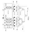
- FIG. 2 is a circuit diagram depicting tile 101 1 and associated failure circuitry in accordance with exemplary embodiments of the present invention.
- tile 101 1 comprises a plurality of bitlines, a plurality of wordlines and a CSL 108 (commonly referred to as a CSL plate).
- Each bitline 110 1 . . . M is driven by a bitline driver 200 1 . . . M , where M is an integer and is variable, prior to fabrication of the device 100 , based on configuration requirements.
- the bitline drivers 200 1 . . . M are each coupled to corresponding data latches 202 1 . . . M .
- a set pulse is applied across several tiles from the tiles 101 1 to 101 N simultaneously.
- a verify-read sequence is performed on each cell prior to the set pulse to verify that the resistance of a cell is lower than a certain resistance threshold to determine whether the cell is in LRS or HRS. If the verify-read pulse determines that the cell resistance is lower than the resistance threshold, the corresponding data latch, e.g., data latch 202 1 , sets a failure bit to “0”. Otherwise, if the verify-read pulse determines that the LRS cell resistance is not lower than the resistance threshold, the failure but is set to “1”, indicating that the memory cell selected by the bitline driver 200 1 is already set to “1”.
- Each data latch 202 has a failure bit set according to the memory cells along each corresponding bitline 110 .
- the data latches 202 are coupled to a collection of OR gates 204 , i.e., a failure circuit.
- the goal of the collection of OR gates 204 1 is to indicate whether this particular tile 101 1 has any memory cells that require a set pulse. If any of the data latches 2021 to 202 M contains a failure bit set to 1 , the output 210 1 (“set_fail_bigor”) will also be “1”, or high (H). Consequently, the output 210 1 is fed to the bitline drivers 200 and the CSL driver 201 for the tile 101 1 .
- each tile 101 1 to 101 N is associated with an identical set of bitline drivers 200 , data latches 202 , collection of OR gates 204 and the output signal of the collection of gates 204 , the output indicating whether a set pulse should be applied to the tile or not. Accordingly, only those tiles with set_fail_bigor (e.g., signal 210 1 ) set to high will raise the CSL and bitline to VSET.
- set_fail_bigor e.g., signal 210 1
- FIG. 3 is a circuit diagram depicting a masking circuit 300 for masking the global CSL signal in accordance with exemplary embodiments of the present invention.
- the circuit comprises an input set_fail_bigor 210 1 (input 210 ), input csl_vss 302 (input 302 ), and input/csl_vset 304 (input 304 ).
- the circuit comprises output signals csl_vss ⁇ 1> 306 (output 308 ) and csl_vset ⁇ 1> 308 (output 308 ) to tile 101 1 . If output 306 is high, the CSL driver 201 for tile 101 1 will bring the CSL to Vss voltage. If output 308 is high, the CSL driver 201 for tile 101 1 will bring the CSL to VSET voltage.
- each tile has an identical circuit between each of the plurality of data latches and the CSL driver/bitline drivers belonging to each tile. Accordingly, each individual tile can mask the global CSL signal and avoid bringing the CSL plate to VSET, thereby reducing power consumption in the memory device 100 .
- the masking circuit 300 further comprises a logical portion for determining the signals at outputs 306 and 308 .
- the logical portion comprising a first inverter 310 , an inverted input AND gate 312 , a second inverter 314 , a second AND gate with inverted output 316 , and an inverted input inverter 318 .
- Output 306 is controlled by input 210 1 and the global signal input 304 .
- output 308 will output HIGH signal.
- the CSL driver 201 will keep the CSL plate 108 and the bitline 110 at Vss. If the output 308 is HIGH and the output 306 is LOW, the CSL driver 201 will raise the CSL plate 108 and the bitline 110 to VSET.
- FIG. 4 is a circuit diagram depicting a common source line driver 201 in accordance with exemplary embodiments of the present invention.
- the CSL driver 201 depicted is coupled to the CSL plate 108 of memory tile 101 1 .
- Each memory tile 101 1 to 101 N has a CSL driver identical to CSL driver 201 , except that inputs 308 and 306 will be from the respective masking circuit associated with the corresponding tile 101 1 to 101 N .
- Each CSL driver determines whether the CSL driver associated with the corresponding tile is driven to VSET or VSS, depending on various inputs.
- the CSL driver 201 comprises a first transistor 400 and a second transistor 402 .
- the source of the transistor 400 is coupled to a VSET voltage source 401 .
- the source of the transistor 402 is coupled to ground (or Vss).
- the input 308 (/csl_vset ⁇ 1>) is coupled to the gate of the transistor 400 .
- the input 306 (/csl_vss ⁇ 1>) is coupled to the gate of the transistor 402 .
- the output of the CSL driver 201 is coupled to the CSL plate 108 for memory tile 101 1 .
- transistor 400 if the masking circuit 300 has an output 308 which is HIGH and an output 306 which is L, the transistor 400 is switched on while transistor 402 is switched off, bringing the CSL 108 up to VSET voltage. Conversely, if the masking circuit 300 has an output 308 which is LOW and an output 306 which is H, the transistor 402 is switched on while transistor 400 is switched off, bringing the CSL 108 to VSS. According to exemplary embodiments, transistor 400 is a p-type transistor.
- FIG. 5 is a circuit diagram depicting a bitline driver 200 1 in accordance with exemplary embodiments of the present invention.
- Each memory tile 101 1 to 101 N has a plurality of bitline drivers identical to bitline driver 200 1 , except that input 306 will be from the respective masking circuit and the data latch will be from the respective bitline associated with the corresponding tile 101 1 to 101 N .
- the bitline driver 200 1 controls whether a bitline of a tile is driven to VSET or VSS.
- Each tile has one bitline for each column of memory cells contained therein.
- the bitline driver 200 1 comprises an input of setpulse_en 501 , set_fail from data latch 202 1 and csl_vss ⁇ 1> 306 .
- Signal 306 is coupled from the masking circuit 300 shown in FIG. 3 .
- the setpulse_en 501 is shared among the data latches 202 and goes HIGH when the set_fail from the data latch 202 1 in each BL is high.
- the set_fail from data latch 202 1 is an indicator of whether the associated bitline is coupled to a memory cell that should be brought to LRS via a set operation.
- the signal csl_vss ⁇ 1> 306 indicates whether the CSL for tile 101 1 should be brought to the VSS voltage.
- the gate of the transistors 508 and 510 are driven according to the data latch output.
- the bitline driver 200 1 comprises a logical portion for determining whether the bitline 110 is drive to VSET or VSS.
- the logical portion of the circuit comprises an inverter 502 , an AND gate with an inverted output 504 and an inverted input OR gate 506 .
- the output of the OR gate 506 is coupled to the gate of transistor 508 and 510 . If the set_fail bit is HIGH and setpulse_en 501 is H, the output of the OR gate 506 goes HIGH. Therefore the voltage signal at the gate of transistor 508 is LOW, while the voltage signal at the gate of transistor 510 is HIGH. Accordingly, transistor 510 is switched on, coupling the bitline 110 to the VSS voltage.
- transistor 508 is a p-type transistor.
- FIG. 6 is a circuit diagram depicting the voltage levels for various signals during a set operation for two memory tiles 101 1 and 101 N in accordance with exemplary embodiments of the present invention.
- the csl set pulse 600 is depicted as initially beginning HIGH, then transitioning to LOW at time t 1 for a period of time before going back to HIGH at time t 6 .
- the csl_vss signal 602 also begins at HIGH, then goes low at time t 1 and remains low until time t 6 .
- the worldine signal 604 begins at LOW and goes to HIGH at time t 2 , and then goes to LOW again at time t 5 .
- the setpulse_en signal 606 goes to HIGH at time t 3 and goes back to LOW at time t 4 .
- the set_fail_bigor ⁇ 1> is HIGH, indicating that a set_fail bit is stored in one of the data latches 202 . Accordingly, the set pulse should be applied to the tile 101 1 by raising the csl ⁇ 1> 610 signal and the bitline signal 612 from Vss to VSET.
- tile 101 N does not have any data latches with a set_fail bit that is HIGH, therefore the set_fail_bigor signal 614 is LOW. Therefore, the CSL plate and all bitlines for tile 101 N remain at Vss voltage. Accordingly, if some portion of the memory tiles in device 100 have their CSL raised to VSET, while some portion of the tiles in device 100 have their CSL and bitline remain at Vss, less power is consumed by device 100 as compared to if all CSL plates and bitlines in memory device 100 were required to be raised to VSET regardless of the status of the status of each memory cell.
Abstract
Description
Claims (11)
Priority Applications (3)
| Application Number | Priority Date | Filing Date | Title |
|---|---|---|---|
| US14/186,636 US9496034B2 (en) | 2013-09-06 | 2014-02-21 | Memory device with a common source line masking circuit |
| KR1020140116107A KR101654418B1 (en) | 2013-09-06 | 2014-09-02 | Memory device with a common source line masking circuit |
| CN201410444511.2A CN104425023B (en) | 2013-09-06 | 2014-09-03 | Memory devices with common source polar curve screened circuit |
Applications Claiming Priority (2)
| Application Number | Priority Date | Filing Date | Title |
|---|---|---|---|
| US201361874417P | 2013-09-06 | 2013-09-06 | |
| US14/186,636 US9496034B2 (en) | 2013-09-06 | 2014-02-21 | Memory device with a common source line masking circuit |
Publications (2)
| Publication Number | Publication Date |
|---|---|
| US20150071010A1 US20150071010A1 (en) | 2015-03-12 |
| US9496034B2 true US9496034B2 (en) | 2016-11-15 |
Family
ID=52625470
Family Applications (1)
| Application Number | Title | Priority Date | Filing Date |
|---|---|---|---|
| US14/186,636 Active US9496034B2 (en) | 2013-09-06 | 2014-02-21 | Memory device with a common source line masking circuit |
Country Status (3)
| Country | Link |
|---|---|
| US (1) | US9496034B2 (en) |
| KR (1) | KR101654418B1 (en) |
| CN (1) | CN104425023B (en) |
Families Citing this family (2)
| Publication number | Priority date | Publication date | Assignee | Title |
|---|---|---|---|---|
| JP6723402B1 (en) * | 2019-02-28 | 2020-07-15 | ウィンボンド エレクトロニクス コーポレーション | Variable resistance random access memory |
| CN111724847A (en) * | 2020-06-03 | 2020-09-29 | 厦门半导体工业技术研发有限公司 | Semiconductor integrated circuit device and method of using the same |
Citations (7)
| Publication number | Priority date | Publication date | Assignee | Title |
|---|---|---|---|---|
| US5412609A (en) * | 1993-04-30 | 1995-05-02 | Kabushiki Kaisha Toshiba | Nonvolatile semiconductor memory device |
| US6356484B2 (en) | 1991-04-18 | 2002-03-12 | Mitsubishi Denki Kabushiki Kaisha | Semiconductor memory device |
| EP1194930B1 (en) | 1999-07-06 | 2004-08-25 | Virage Logic Corporation | Multi-bank memory with word-line banking, bit-line banking and i/o multiplexing utilizing tilable interconnects |
| WO2009086618A1 (en) | 2008-01-07 | 2009-07-16 | Mosaid Technologies Incorporated | Nand flash memory having multiple cell substrates |
| EP2169684A1 (en) | 2005-03-16 | 2010-03-31 | Sandisk Corporation | Non-volatile memory and method with power-saving read and program-verify operations |
| US20100080066A1 (en) * | 2008-09-26 | 2010-04-01 | Fujitsu Microelectronics Limited | Memory, memory operating method, and memory system |
| US20110194361A1 (en) * | 2008-10-06 | 2011-08-11 | Takayuki Kawahara | Semiconductor device |
Family Cites Families (3)
| Publication number | Priority date | Publication date | Assignee | Title |
|---|---|---|---|---|
| US7978518B2 (en) * | 2007-12-21 | 2011-07-12 | Mosaid Technologies Incorporated | Hierarchical common source line structure in NAND flash memory |
| KR101491829B1 (en) * | 2008-08-14 | 2015-02-12 | 삼성전자주식회사 | Memory apparatus protected from read disturbance and method thereof |
| WO2011134055A1 (en) * | 2010-04-26 | 2011-11-03 | Mosaid Technologies Incorporated | Write scheme in phase change memory |
-
2014
- 2014-02-21 US US14/186,636 patent/US9496034B2/en active Active
- 2014-09-02 KR KR1020140116107A patent/KR101654418B1/en active IP Right Grant
- 2014-09-03 CN CN201410444511.2A patent/CN104425023B/en not_active Expired - Fee Related
Patent Citations (7)
| Publication number | Priority date | Publication date | Assignee | Title |
|---|---|---|---|---|
| US6356484B2 (en) | 1991-04-18 | 2002-03-12 | Mitsubishi Denki Kabushiki Kaisha | Semiconductor memory device |
| US5412609A (en) * | 1993-04-30 | 1995-05-02 | Kabushiki Kaisha Toshiba | Nonvolatile semiconductor memory device |
| EP1194930B1 (en) | 1999-07-06 | 2004-08-25 | Virage Logic Corporation | Multi-bank memory with word-line banking, bit-line banking and i/o multiplexing utilizing tilable interconnects |
| EP2169684A1 (en) | 2005-03-16 | 2010-03-31 | Sandisk Corporation | Non-volatile memory and method with power-saving read and program-verify operations |
| WO2009086618A1 (en) | 2008-01-07 | 2009-07-16 | Mosaid Technologies Incorporated | Nand flash memory having multiple cell substrates |
| US20100080066A1 (en) * | 2008-09-26 | 2010-04-01 | Fujitsu Microelectronics Limited | Memory, memory operating method, and memory system |
| US20110194361A1 (en) * | 2008-10-06 | 2011-08-11 | Takayuki Kawahara | Semiconductor device |
Non-Patent Citations (1)
| Title |
|---|
| Smart Charge Prior Art Search Report, 15 Pages, Oct. 10, 2013. |
Also Published As
| Publication number | Publication date |
|---|---|
| KR101654418B1 (en) | 2016-09-05 |
| CN104425023B (en) | 2018-02-23 |
| US20150071010A1 (en) | 2015-03-12 |
| CN104425023A (en) | 2015-03-18 |
| KR20150028726A (en) | 2015-03-16 |
Similar Documents
| Publication | Publication Date | Title |
|---|---|---|
| US20200365205A1 (en) | High voltage switching circuitry for a cross-point array | |
| US8144499B2 (en) | Variable resistance memory device | |
| US8750017B2 (en) | Resistance-change memory | |
| US20070041235A1 (en) | Semiconductor storage device | |
| US9318158B2 (en) | Non-volatile memory using bi-directional resistive elements | |
| US8705266B2 (en) | Semiconductor device and method for controlling the same | |
| US9361976B2 (en) | Sense amplifier including a single-transistor amplifier and level shifter and methods therefor | |
| US9805793B2 (en) | Filament confinement in reversible resistance-switching memory elements | |
| US10553647B2 (en) | Methods and apparatus for three-dimensional non-volatile memory | |
| US20100208510A1 (en) | Semiconductor memory device and method of operating the same | |
| US20180166138A1 (en) | Resistance variable element methods and apparatuses | |
| US9099176B1 (en) | Resistive switching memory device with diode select | |
| JP2011198445A (en) | Semiconductor memory | |
| US9401207B2 (en) | Pseudo SRAM using resistive elements for non-volatile storage | |
| US7616486B2 (en) | Cell array of semiconductor memory device and method of driving the same | |
| US8493768B2 (en) | Memory cell and memory device using the same | |
| US9496034B2 (en) | Memory device with a common source line masking circuit | |
| US10355049B1 (en) | Methods and apparatus for three-dimensional non-volatile memory | |
| CN107799146B (en) | Memory array and reading, programming and erasing operation method thereof | |
| WO2015182100A1 (en) | Semiconductor storage device | |
| US9093147B2 (en) | Method and apparatus for common source line charge transfer | |
| US20230282277A1 (en) | Semiconductor device and method of controlling the same | |
| US20120155204A1 (en) | Semiconductor memory apparatus having a pre-discharging function, semiconductor integrated circuit having the same, and method for driving the same | |
| US20110305062A1 (en) | Memory cell and memory device using the same | |
| CN109215710B (en) | Memory cell and memory |
Legal Events
| Date | Code | Title | Description |
|---|---|---|---|
| AS | Assignment |
Owner name: SONY CORPORATION, JAPAN Free format text: ASSIGNMENT OF ASSIGNORS INTEREST;ASSIGNORS:KITAGAWA, MAKOTO;JAVANIFARD, JAHANSHIR;SIGNING DATES FROM 20140205 TO 20140403;REEL/FRAME:032613/0252 |
|
| AS | Assignment |
Owner name: SONY SEMICONDUCTOR SOLUTIONS CORPORATION, JAPAN Free format text: CHANGE OF NAME;ASSIGNOR:SONY CORPORATION;REEL/FRAME:039635/0495 Effective date: 20160714 |
|
| STCF | Information on status: patent grant |
Free format text: PATENTED CASE |
|
| FEPP | Fee payment procedure |
Free format text: PAYOR NUMBER ASSIGNED (ORIGINAL EVENT CODE: ASPN); ENTITY STATUS OF PATENT OWNER: LARGE ENTITY |
|
| AS | Assignment |
Owner name: SONY SEMICONDUCTOR SOLUTIONS CORPORATION, JAPAN Free format text: CORRECTIVE ASSIGNMENT TO CORRECT THE NATURE OF CONVEYANCE PREVIOUSLY RECORDED ON REEL 039635 FRAME 0495. ASSIGNOR(S) HEREBY CONFIRMS THE ASSIGNMENT;ASSIGNOR:SONY CORPORATION;REEL/FRAME:040815/0649 Effective date: 20160714 |
|
| MAFP | Maintenance fee payment |
Free format text: PAYMENT OF MAINTENANCE FEE, 4TH YEAR, LARGE ENTITY (ORIGINAL EVENT CODE: M1551); ENTITY STATUS OF PATENT OWNER: LARGE ENTITY Year of fee payment: 4 |
|
| AS | Assignment |
Owner name: SONY SEMICONDUCTOR SOLUTIONS CORPORATION, JAPAN Free format text: CORRECTIVE ASSIGNMENT TO CORRECT THE REMOVE INCORRECT APPLICATION NUMBER 14/572221 AND REPLACE IT WITH 14/527221 PREVIOUSLY RECORDED AT REEL: 040815 FRAME: 0649. ASSIGNOR(S) HEREBY CONFIRMS THE ASSIGNMENT;ASSIGNOR:SONY CORPORATION;REEL/FRAME:058875/0887 Effective date: 20160714 |