US9461041B2 - Metal gate finFET device - Google Patents
Metal gate finFET device Download PDFInfo
- Publication number
- US9461041B2 US9461041B2 US14/584,783 US201414584783A US9461041B2 US 9461041 B2 US9461041 B2 US 9461041B2 US 201414584783 A US201414584783 A US 201414584783A US 9461041 B2 US9461041 B2 US 9461041B2
- Authority
- US
- United States
- Prior art keywords
- metal layer
- fin
- metal
- layer
- fins
- Prior art date
- Legal status (The legal status is an assumption and is not a legal conclusion. Google has not performed a legal analysis and makes no representation as to the accuracy of the status listed.)
- Active
Links
- 229910052751 metal Inorganic materials 0.000 title claims abstract description 156
- 239000002184 metal Substances 0.000 title claims abstract description 156
- 239000000758 substrate Substances 0.000 claims abstract description 44
- 238000002955 isolation Methods 0.000 claims description 20
- 239000000203 mixture Substances 0.000 claims description 14
- 229910052710 silicon Inorganic materials 0.000 claims description 10
- 239000010703 silicon Substances 0.000 claims description 10
- ATJFFYVFTNAWJD-UHFFFAOYSA-N Tin Chemical compound [Sn] ATJFFYVFTNAWJD-UHFFFAOYSA-N 0.000 claims description 7
- 229910052782 aluminium Inorganic materials 0.000 claims description 4
- 229910002091 carbon monoxide Inorganic materials 0.000 claims description 4
- 229910052802 copper Inorganic materials 0.000 claims description 4
- 229910052741 iridium Inorganic materials 0.000 claims description 3
- 229910052759 nickel Inorganic materials 0.000 claims description 3
- 229910052702 rhenium Inorganic materials 0.000 claims description 3
- 150000004767 nitrides Chemical class 0.000 claims 1
- 229910052721 tungsten Inorganic materials 0.000 claims 1
- 239000010410 layer Substances 0.000 description 152
- 238000000034 method Methods 0.000 description 57
- 239000004065 semiconductor Substances 0.000 description 29
- 238000000231 atomic layer deposition Methods 0.000 description 12
- 238000005240 physical vapour deposition Methods 0.000 description 12
- 239000000463 material Substances 0.000 description 11
- VYPSYNLAJGMNEJ-UHFFFAOYSA-N Silicium dioxide Chemical compound O=[Si]=O VYPSYNLAJGMNEJ-UHFFFAOYSA-N 0.000 description 10
- XUIMIQQOPSSXEZ-UHFFFAOYSA-N Silicon Chemical compound [Si] XUIMIQQOPSSXEZ-UHFFFAOYSA-N 0.000 description 9
- 238000005229 chemical vapour deposition Methods 0.000 description 8
- 125000006850 spacer group Chemical group 0.000 description 7
- 230000005669 field effect Effects 0.000 description 6
- 238000004519 manufacturing process Methods 0.000 description 6
- 229910044991 metal oxide Inorganic materials 0.000 description 6
- 150000004706 metal oxides Chemical class 0.000 description 6
- 229920002120 photoresistant polymer Polymers 0.000 description 6
- 229910021420 polycrystalline silicon Inorganic materials 0.000 description 6
- 229920005591 polysilicon Polymers 0.000 description 6
- 229910052814 silicon oxide Inorganic materials 0.000 description 6
- 239000003989 dielectric material Substances 0.000 description 5
- 238000000623 plasma-assisted chemical vapour deposition Methods 0.000 description 5
- 239000000126 substance Substances 0.000 description 5
- 229910052581 Si3N4 Inorganic materials 0.000 description 4
- 238000005530 etching Methods 0.000 description 4
- 230000000873 masking effect Effects 0.000 description 4
- 230000003647 oxidation Effects 0.000 description 4
- 238000007254 oxidation reaction Methods 0.000 description 4
- HQVNEWCFYHHQES-UHFFFAOYSA-N silicon nitride Chemical compound N12[Si]34N5[Si]62N3[Si]51N64 HQVNEWCFYHHQES-UHFFFAOYSA-N 0.000 description 4
- 230000015572 biosynthetic process Effects 0.000 description 3
- 239000003990 capacitor Substances 0.000 description 3
- 230000000295 complement effect Effects 0.000 description 3
- 238000000151 deposition Methods 0.000 description 3
- 239000005350 fused silica glass Substances 0.000 description 3
- 238000000206 photolithography Methods 0.000 description 3
- 229910000577 Silicon-germanium Inorganic materials 0.000 description 2
- BOTDANWDWHJENH-UHFFFAOYSA-N Tetraethyl orthosilicate Chemical compound CCO[Si](OCC)(OCC)OCC BOTDANWDWHJENH-UHFFFAOYSA-N 0.000 description 2
- GWEVSGVZZGPLCZ-UHFFFAOYSA-N Titan oxide Chemical compound O=[Ti]=O GWEVSGVZZGPLCZ-UHFFFAOYSA-N 0.000 description 2
- MCMNRKCIXSYSNV-UHFFFAOYSA-N Zirconium dioxide Chemical compound O=[Zr]=O MCMNRKCIXSYSNV-UHFFFAOYSA-N 0.000 description 2
- 229910045601 alloy Inorganic materials 0.000 description 2
- 239000000956 alloy Substances 0.000 description 2
- 239000005380 borophosphosilicate glass Substances 0.000 description 2
- 150000001875 compounds Chemical class 0.000 description 2
- 230000003247 decreasing effect Effects 0.000 description 2
- 238000005516 engineering process Methods 0.000 description 2
- 230000006870 function Effects 0.000 description 2
- 229910052732 germanium Inorganic materials 0.000 description 2
- GNPVGFCGXDBREM-UHFFFAOYSA-N germanium atom Chemical compound [Ge] GNPVGFCGXDBREM-UHFFFAOYSA-N 0.000 description 2
- 238000004518 low pressure chemical vapour deposition Methods 0.000 description 2
- 238000000059 patterning Methods 0.000 description 2
- 239000005360 phosphosilicate glass Substances 0.000 description 2
- 239000005368 silicate glass Substances 0.000 description 2
- 230000003068 static effect Effects 0.000 description 2
- 229910000980 Aluminium gallium arsenide Inorganic materials 0.000 description 1
- JBRZTFJDHDCESZ-UHFFFAOYSA-N AsGa Chemical compound [As]#[Ga] JBRZTFJDHDCESZ-UHFFFAOYSA-N 0.000 description 1
- ZOXJGFHDIHLPTG-UHFFFAOYSA-N Boron Chemical compound [B] ZOXJGFHDIHLPTG-UHFFFAOYSA-N 0.000 description 1
- 229910005540 GaP Inorganic materials 0.000 description 1
- 229910000530 Gallium indium arsenide Inorganic materials 0.000 description 1
- -1 HfZrO Inorganic materials 0.000 description 1
- 229910000673 Indium arsenide Inorganic materials 0.000 description 1
- GPXJNWSHGFTCBW-UHFFFAOYSA-N Indium phosphide Chemical compound [In]#P GPXJNWSHGFTCBW-UHFFFAOYSA-N 0.000 description 1
- 229910004481 Ta2O3 Inorganic materials 0.000 description 1
- 230000004075 alteration Effects 0.000 description 1
- 229910021417 amorphous silicon Inorganic materials 0.000 description 1
- 229910052796 boron Inorganic materials 0.000 description 1
- 230000015556 catabolic process Effects 0.000 description 1
- 238000006731 degradation reaction Methods 0.000 description 1
- 230000008021 deposition Effects 0.000 description 1
- 238000005137 deposition process Methods 0.000 description 1
- 238000011161 development Methods 0.000 description 1
- 230000018109 developmental process Effects 0.000 description 1
- 229910003460 diamond Inorganic materials 0.000 description 1
- 239000010432 diamond Substances 0.000 description 1
- 238000001312 dry etching Methods 0.000 description 1
- HZXMRANICFIONG-UHFFFAOYSA-N gallium phosphide Chemical compound [Ga]#P HZXMRANICFIONG-UHFFFAOYSA-N 0.000 description 1
- 239000011521 glass Substances 0.000 description 1
- CJNBYAVZURUTKZ-UHFFFAOYSA-N hafnium(iv) oxide Chemical compound O=[Hf]=O CJNBYAVZURUTKZ-UHFFFAOYSA-N 0.000 description 1
- 229910000167 hafnon Inorganic materials 0.000 description 1
- WPYVAWXEWQSOGY-UHFFFAOYSA-N indium antimonide Chemical compound [Sb]#[In] WPYVAWXEWQSOGY-UHFFFAOYSA-N 0.000 description 1
- RPQDHPTXJYYUPQ-UHFFFAOYSA-N indium arsenide Chemical compound [In]#[As] RPQDHPTXJYYUPQ-UHFFFAOYSA-N 0.000 description 1
- 239000012212 insulator Substances 0.000 description 1
- 239000011229 interlayer Substances 0.000 description 1
- 150000002500 ions Chemical class 0.000 description 1
- 230000000670 limiting effect Effects 0.000 description 1
- 235000012054 meals Nutrition 0.000 description 1
- 238000005498 polishing Methods 0.000 description 1
- 230000002829 reductive effect Effects 0.000 description 1
- 229910010271 silicon carbide Inorganic materials 0.000 description 1
- HBMJWWWQQXIZIP-UHFFFAOYSA-N silicon carbide Chemical compound [Si+]#[C-] HBMJWWWQQXIZIP-UHFFFAOYSA-N 0.000 description 1
- 239000000377 silicon dioxide Substances 0.000 description 1
- 235000012239 silicon dioxide Nutrition 0.000 description 1
- 238000006467 substitution reaction Methods 0.000 description 1
- 238000001039 wet etching Methods 0.000 description 1
Images


Classifications
-
- H—ELECTRICITY
- H01—ELECTRIC ELEMENTS
- H01L—SEMICONDUCTOR DEVICES NOT COVERED BY CLASS H10
- H01L27/00—Devices consisting of a plurality of semiconductor or other solid-state components formed in or on a common substrate
- H01L27/02—Devices consisting of a plurality of semiconductor or other solid-state components formed in or on a common substrate including semiconductor components specially adapted for rectifying, oscillating, amplifying or switching and having potential barriers; including integrated passive circuit elements having potential barriers
- H01L27/04—Devices consisting of a plurality of semiconductor or other solid-state components formed in or on a common substrate including semiconductor components specially adapted for rectifying, oscillating, amplifying or switching and having potential barriers; including integrated passive circuit elements having potential barriers the substrate being a semiconductor body
- H01L27/08—Devices consisting of a plurality of semiconductor or other solid-state components formed in or on a common substrate including semiconductor components specially adapted for rectifying, oscillating, amplifying or switching and having potential barriers; including integrated passive circuit elements having potential barriers the substrate being a semiconductor body including only semiconductor components of a single kind
- H01L27/085—Devices consisting of a plurality of semiconductor or other solid-state components formed in or on a common substrate including semiconductor components specially adapted for rectifying, oscillating, amplifying or switching and having potential barriers; including integrated passive circuit elements having potential barriers the substrate being a semiconductor body including only semiconductor components of a single kind including field-effect components only
- H01L27/088—Devices consisting of a plurality of semiconductor or other solid-state components formed in or on a common substrate including semiconductor components specially adapted for rectifying, oscillating, amplifying or switching and having potential barriers; including integrated passive circuit elements having potential barriers the substrate being a semiconductor body including only semiconductor components of a single kind including field-effect components only the components being field-effect transistors with insulated gate
- H01L27/0886—Devices consisting of a plurality of semiconductor or other solid-state components formed in or on a common substrate including semiconductor components specially adapted for rectifying, oscillating, amplifying or switching and having potential barriers; including integrated passive circuit elements having potential barriers the substrate being a semiconductor body including only semiconductor components of a single kind including field-effect components only the components being field-effect transistors with insulated gate including transistors with a horizontal current flow in a vertical sidewall of a semiconductor body, e.g. FinFET, MuGFET
-
- H—ELECTRICITY
- H01—ELECTRIC ELEMENTS
- H01L—SEMICONDUCTOR DEVICES NOT COVERED BY CLASS H10
- H01L29/00—Semiconductor devices specially adapted for rectifying, amplifying, oscillating or switching and having potential barriers; Capacitors or resistors having potential barriers, e.g. a PN-junction depletion layer or carrier concentration layer; Details of semiconductor bodies or of electrodes thereof ; Multistep manufacturing processes therefor
- H01L29/66—Types of semiconductor device ; Multistep manufacturing processes therefor
- H01L29/66007—Multistep manufacturing processes
- H01L29/66075—Multistep manufacturing processes of devices having semiconductor bodies comprising group 14 or group 13/15 materials
- H01L29/66227—Multistep manufacturing processes of devices having semiconductor bodies comprising group 14 or group 13/15 materials the devices being controllable only by the electric current supplied or the electric potential applied, to an electrode which does not carry the current to be rectified, amplified or switched, e.g. three-terminal devices
- H01L29/66409—Unipolar field-effect transistors
- H01L29/66477—Unipolar field-effect transistors with an insulated gate, i.e. MISFET
- H01L29/66545—Unipolar field-effect transistors with an insulated gate, i.e. MISFET using a dummy, i.e. replacement gate in a process wherein at least a part of the final gate is self aligned to the dummy gate
-
- H—ELECTRICITY
- H01—ELECTRIC ELEMENTS
- H01L—SEMICONDUCTOR DEVICES NOT COVERED BY CLASS H10
- H01L29/00—Semiconductor devices specially adapted for rectifying, amplifying, oscillating or switching and having potential barriers; Capacitors or resistors having potential barriers, e.g. a PN-junction depletion layer or carrier concentration layer; Details of semiconductor bodies or of electrodes thereof ; Multistep manufacturing processes therefor
- H01L29/02—Semiconductor bodies ; Multistep manufacturing processes therefor
- H01L29/06—Semiconductor bodies ; Multistep manufacturing processes therefor characterised by their shape; characterised by the shapes, relative sizes, or dispositions of the semiconductor regions ; characterised by the concentration or distribution of impurities within semiconductor regions
- H01L29/0603—Semiconductor bodies ; Multistep manufacturing processes therefor characterised by their shape; characterised by the shapes, relative sizes, or dispositions of the semiconductor regions ; characterised by the concentration or distribution of impurities within semiconductor regions characterised by particular constructional design considerations, e.g. for preventing surface leakage, for controlling electric field concentration or for internal isolations regions
- H01L29/0642—Isolation within the component, i.e. internal isolation
- H01L29/0649—Dielectric regions, e.g. SiO2 regions, air gaps
-
- H—ELECTRICITY
- H01—ELECTRIC ELEMENTS
- H01L—SEMICONDUCTOR DEVICES NOT COVERED BY CLASS H10
- H01L29/00—Semiconductor devices specially adapted for rectifying, amplifying, oscillating or switching and having potential barriers; Capacitors or resistors having potential barriers, e.g. a PN-junction depletion layer or carrier concentration layer; Details of semiconductor bodies or of electrodes thereof ; Multistep manufacturing processes therefor
- H01L29/66—Types of semiconductor device ; Multistep manufacturing processes therefor
- H01L29/66007—Multistep manufacturing processes
- H01L29/66075—Multistep manufacturing processes of devices having semiconductor bodies comprising group 14 or group 13/15 materials
- H01L29/66227—Multistep manufacturing processes of devices having semiconductor bodies comprising group 14 or group 13/15 materials the devices being controllable only by the electric current supplied or the electric potential applied, to an electrode which does not carry the current to be rectified, amplified or switched, e.g. three-terminal devices
- H01L29/66409—Unipolar field-effect transistors
- H01L29/66477—Unipolar field-effect transistors with an insulated gate, i.e. MISFET
- H01L29/66787—Unipolar field-effect transistors with an insulated gate, i.e. MISFET with a gate at the side of the channel
- H01L29/66795—Unipolar field-effect transistors with an insulated gate, i.e. MISFET with a gate at the side of the channel with a horizontal current flow in a vertical sidewall of a semiconductor body, e.g. FinFET, MuGFET
-
- H—ELECTRICITY
- H01—ELECTRIC ELEMENTS
- H01L—SEMICONDUCTOR DEVICES NOT COVERED BY CLASS H10
- H01L29/00—Semiconductor devices specially adapted for rectifying, amplifying, oscillating or switching and having potential barriers; Capacitors or resistors having potential barriers, e.g. a PN-junction depletion layer or carrier concentration layer; Details of semiconductor bodies or of electrodes thereof ; Multistep manufacturing processes therefor
- H01L29/66—Types of semiconductor device ; Multistep manufacturing processes therefor
- H01L29/68—Types of semiconductor device ; Multistep manufacturing processes therefor controllable by only the electric current supplied, or only the electric potential applied, to an electrode which does not carry the current to be rectified, amplified or switched
- H01L29/76—Unipolar devices, e.g. field effect transistors
- H01L29/772—Field effect transistors
- H01L29/78—Field effect transistors with field effect produced by an insulated gate
- H01L29/7842—Field effect transistors with field effect produced by an insulated gate means for exerting mechanical stress on the crystal lattice of the channel region, e.g. using a flexible substrate
- H01L29/7845—Field effect transistors with field effect produced by an insulated gate means for exerting mechanical stress on the crystal lattice of the channel region, e.g. using a flexible substrate the means being a conductive material, e.g. silicided S/D or Gate
Definitions
- finFET fin field effect transistor
- FinFET devices are so called because a gate is formed on and around a “fin” that extends from the substrate.
- a finFET device is any fin-based, multigate transistor. FinFET devices may allow for shrinking the gate width of device while providing a gate on the sides and/or top of the fin including the channel region.
- Another advancement implemented as technology nodes shrink, in some IC designs, has been the replacement of the typically polysilicon gate electrode with a metal gate electrode to improve device performance with the decreased feature sizes.
- One method of forming the metal gate electrode is a “gate last” or “replacement gate” methodology where a dummy gate, typically polysilicon is replaced by a metal gate. Providing the metal gate later in the process can avoid problems of the stability of the work function metal during processing.
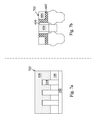
- FIG. 1 is perspective view of an embodiment of a finFET device according to one or more aspects of the present disclosure.
- FIG. 2 is a cross-sectional view of an embodiment of a finFET device according to one or more aspects of the present disclosure.
- FIG. 3 is a flow chart of a method of fabricating a finFET device according to one or more aspects of the present disclosure.
- FIGS. 4 a -13 b illustrate cross sectional views of an embodiment of a finFET device corresponding to one or more steps of the method of FIG. 3 .
- FIGS. 4 a , 5 a , 6 a , 7 a , 8 a , 9 a , 10 a , 11 a , 12 a , and 13 a are provided along cross-sectional view substantially similar to section AA of FIG. 1 .
- FIGS. 4 b , 5 b , 6 b , 7 b , 8 b , 9 b , 10 b , 11 b , 12 b , and 13 b are provided along cross-sectional view substantially similar to section BB of FIG. 1 .
- first and second features are formed in direct contact
- additional features may be formed interposing the first and second features, such that the first and second features may not be in direct contact.
- Various features may be arbitrarily drawn in different scales for simplicity and clarity.
- the present disclosure presents embodiments in the form of multi-gate transistors or fin-type multi-gate transistors referred to herein as finFET devices.
- a device may include a p-type metal oxide semiconductor finFET device or an n-type metal oxide semiconductor finFET device.
- the finFET device may be a dual-gate device, tri-gate device, and/or other configuration.
- One of ordinary skill may recognize other embodiments of semiconductor devices that may benefit from aspects of the present disclosure.
- the finFET device 100 includes one or more fin-based, multigate field effect transistors.
- the finFET device 100 includes a substrate 102 , a fin-element 104 extending from the substrate 102 , isolation regions 106 , and a gate structure 108 disposed on and around the fin-element 104 .
- the substrate 102 may be a semiconductor substrate such as a silicon substrate.
- the substrate may include various layers, including conductive or insulative layers formed on a semiconductor substrate.
- the substrate may include various doping configurations depending on design requirements as is known in the art.
- the substrate may also include other elementary semiconductors such as germanium and diamond.
- the substrate may include a compound semiconductor and/or an alloy semiconductor.
- the substrate may optionally include an epitaxial layer (epi layer), may be strained for performance enhancement, may include a silicon-on-insulator (SOI) structure, and/or have other suitable enhancement features.
- epi layer epitaxial layer
- SOI silicon-on-insulator
- the fin-element 104 may comprise silicon or another elementary semiconductor, such as germanium; a compound semiconductor including silicon carbide, gallium arsenic, gallium phosphide, indium phosphide, indium arsenide, and/or indium antimonide; an alloy semiconductor including SiGe, GaAsP, AlInAs, AlGaAs, GaInAs, GaInP, and/or GaInAsP; or combinations thereof.
- the fins 102 may be fabricated using suitable processes including photolithography and etch processes.
- the photolithography process may include forming a photoresist layer (resist) overlying the substrate (e.g., on a silicon layer), exposing the resist to a pattern, performing post-exposure bake processes, and developing the resist to form a masking element including the resist.
- the masking element may then be used to protect regions of the substrate while an etch process forms recesses into the silicon layer, leaving an extending fin.
- the recesses may be etched using reactive ion etch (RIE) and/or other suitable processes. Numerous other embodiments of methods to form the fins 104 on the substrate 102 may be suitable.
- RIE reactive ion etch
- Each of the plurality of fins 104 include a source/drain region where a source or drain feature is formed in, on, and/or surrounding the fin 104 .
- a channel region of a transistor is disposed in the fin 104 underlies the gate structure 108 .
- the isolation regions 106 may be shallow trench isolation (STI) features. Alternatively, field oxide, a LOCOS feature, and/or other suitable isolation features may be implemented on the substrate 102 .
- the isolation regions 106 may be formed of silicon oxide, silicon nitride, silicon oxynitride, fluoride-doped silicate glass (FSG), a low-k dielectric, combinations thereof, and/or other suitable material known in the art.
- the isolation structures are STI features and are formed by etching trenches in the substrate 102 . The trenches may then be filled with isolating material, followed by a chemical mechanical polish (CMP).
- CMP chemical mechanical polish
- the isolation regions 106 may include a multi-layer structure, for example, having one or more liner layers.
- the gate structure 108 includes a first metal layer 110 and a second metal layer 112 .
- the first metal layer 110 may be a stress metal layer.
- the second metal layer 112 may be a conduction metal layer.
- the first metal layer 110 is filled over the fin height, such that it extends on and above a top surface of the fin 104 . This is described in further detail with respect to FIG. 2 .
- the first metal layer 110 may provide for a stress to the gate.
- the second metal layer 112 may provide for a lower gate resistance (e.g., lower than a gate structure having exclusively a composition of the first metal layer 110 ).
- ⁇ sm is the resistivity of the first metal layer 110 .
- ⁇ cm is the resistivity of the second metal layer 112 .
- L g is the length of the gate as illustrated in FIG. 1 .
- H sm , H fin , H cm are detailed below with reference to FIG. 2 .
- Exemplary compositions for the first metal layer 110 include W, TiN, TaN, WN, Re, Ir, Ru, Mo, combinations thereof, and/or other suitable compositions.
- the first metal layer 110 may be formed using chemical vapor deposition, atomic layer deposition, and/or other suitable process.
- the first metal layer 110 includes W having a Young's modulus of approximately 400-410 GPa, deposited, for example, by CVD.
- the first metal layer 110 includes TiN having a Young's modulus of approximately 251-550 GPa, deposited, for example, by atomic layer deposition (ALD).
- the first metal layer 110 includes TaN deposited by ALD.
- the first metal layer 110 includes WN deposited by CVD.
- the first metal layer 110 includes Re having a Young's modulus of approximately 463 GPa; Ir having a Young's modulus of approximately 528 GPa; Ru having a Young's modulus of approximately 447 GPa; or Mo having a Young's modulus of approximately 329 GPa.
- Exemplary compositions for the second metal layer 112 include Al, Cu, CO, Ni, combinations thereof, and/or other suitable compositions.
- the second metal layer 112 may be formed using physical vapor deposition and/or other suitable process.
- the second metal layer 112 includes Al having a resistivity of 2.7E10 ⁇ 8 ⁇ m, deposited, for example, by physical vapor deposition (PVD).
- the second metal layer 112 includes Cu having a resistivity of 1.72*10 ⁇ 8 ⁇ m, deposited, for example, by PVD.
- the second metal layer 112 includes Co having a resistivity of 6*10 ⁇ 8 ⁇ m, deposited, for example, by PVD.
- the second metal layer 112 includes Ni having a resistivity of 7.2*10 ⁇ 8 ⁇ m, deposited, for example, by PVD.
- the gate structure 108 may further include an interfacial layer and/or gate dielectric layer.
- the interfacial layer may include a dielectric material such as silicon oxide layer (SiO 2 ) or silicon oxynitride (SiON).
- the interfacial layer may be formed by chemical oxidation, thermal oxidation, atomic layer deposition (ALD), chemical vapor deposition (CVD), and/or other suitable method.
- the gate dielectric layer may include a high-k dielectric layer such as hafnium oxide (HfO 2 ).
- the high-k dielectric layer may optionally include other high-k dielectrics, such as TiO 2 , HfZrO, Ta 2 O 3 , HfSiO 4 , ZrO 2 , ZrSiO 2 , combinations thereof, or other suitable material.
- the gate dielectric layer may include silicon dioxide or other suitable dielectric.
- the dielectric layer may be formed by atomic layer deposition (ALD), oxidation, and/or other suitable methods.
- the dielectric layer(s) may underlie the first and/or second metal layers 110 , 112 .
- the first metal layer 110 is formed directly on the gate dielectric layer.
- FIG. 2 provides a cross-sectional view of the device 100 at A-A.
- the gate structure 108 has a gate height (H gate ) extending from a top surface of the gate structure (e.g., top of the second metal 112 ) to the top surface of the fin 104 .
- the H gate may be between approximately 20 nanometers (nm) and approximately 60 nm, by way of example.
- the fin 104 may extend a height H fin above the isolation region 106 .
- the H fin may be between approximately 10 nm and approximately 40 nm, by way of example.
- the first metal layer 110 (e.g., stress metal) includes a height H sm .
- H sm is greater than H fin .
- the H sm may be between approximately 20 nm and approximately 70 nm, by way of example.
- the device 100 may provide the relationship: H fin ⁇ H sm ⁇ ( H fin ( H gate /2)) or H fin may be less than H sm (height of the first metal); H sm (height of the first metal) is less than H fin +half of H gate , as illustrated in FIG. 2 .
- the device 100 is illustrative of a finFET device (e.g., semiconductor device including one or more fin-based transistors) having a first, stress metal layer and a second, conduction metal layer included in its gate structure. This may provide for a stronger stress than a planar transistor.
- a finFET device e.g., semiconductor device including one or more fin-based transistors
- This may provide for a stronger stress than a planar transistor.
- the device 100 may be an intermediate device fabricated during processing of an integrated circuit, or portion thereof, that may comprise static random access memory (SRAM) and/or other logic circuits, passive components such as resistors, capacitors, and inductors, and active components such as P-channel field effect transistors (PFET), N-channel FET (NFET), metal-oxide semiconductor field effect transistors (MOSFET), complementary metal-oxide semiconductor (CMOS) transistors, bipolar transistors, high voltage transistors, high frequency transistors, other memory cells, and combinations thereof.
- SRAM static random access memory
- PFET P-channel field effect transistors
- NFET N-channel FET
- MOSFET metal-oxide semiconductor field effect transistors
- CMOS complementary metal-oxide semiconductor
- FIG. 3 illustrated is a method 300 of fabricating a semiconductor device including a finFET device.
- the method 300 may be used to implement a metal gate structure on a fin-based semiconductor device.
- the method 300 may be used to fabricate the device 100 , described above with reference to FIGS. 1 and 2 .
- FIGS. 4-12 are cross-sectional views of an exemplary device 400 fabricating according to one or more steps of the method 300 of FIG. 3 .
- CMOS complementary metal-oxide-semiconductor
- the semiconductor device 400 may include various other devices and features, such as additional transistors, bipolar junction transistors, resistors, capacitors, diodes, fuses, etc., but is simplified for a better understanding of the inventive concepts of the present disclosure.
- the semiconductor device 400 includes a plurality of semiconductor devices (e.g., transistors), which may be interconnected.
- the device 400 may be an intermediate device fabricated during processing of an integrated circuit, or portion thereof, that may comprise static random access memory (SRAM) and/or other logic circuits, passive components such as resistors, capacitors, and inductors, and active components such as P-channel field effect transistors (PFET), N-channel FET (NFET), metal-oxide semiconductor field effect transistors (MOSFET), complementary metal-oxide semiconductor (CMOS) transistors, bipolar transistors, high voltage transistors, high frequency transistors, other memory cells, and combinations thereof.
- SRAM static random access memory
- PFET P-channel field effect transistors
- NFET N-channel FET
- MOSFET metal-oxide semiconductor field effect transistors
- CMOS complementary metal-oxide semiconductor
- the method 300 begins at block 302 where a substrate is provided.
- the substrate has one or more fins extending from the substrate. Isolation regions (e.g., STI features) may interpose the fins.
- Isolation regions e.g., STI features
- the substrate may be substantially similar to the substrate (including the fins and isolation regions) discussed above with reference to FIGS. 1 and/or 2 .
- the semiconductor device 400 includes a semiconductor substrate 102 , a plurality of fins 104 extending from the substrate 102 , and isolation regions 106 .
- the isolation regions 106 are STI features.
- the semiconductor device 400 further includes source/drain regions 402 formed on/in the fin 104 .
- the source/drain regions 402 include epitaxially grown regions, for example, SiGe regions formed in a silicon fin 104 .
- the source/drain regions 402 may be suitably doped to provide N-type or P-type regions.
- the source/drain regions 402 may be formed after the formation of the dummy gate structures, discussed below with reference to block 304 .
- the method 300 then proceeds to block 304 where a dummy gate structure is formed on one or more of the fins.
- the dummy gate structure includes one or more sacrificial layers, which are subsequently removed from the substrate as discussed before with reference to block 308 .
- the dummy gate structures may include polysilicon, amorphous silicon, and/or other suitable material.
- the dummy gate structure may include layers that are not removed from the substrate, for example, gate dielectric layers, work function layers, interfacial layers, and/or other suitable layers.
- the initially formed gate dielectric layer (e.g., SiO 2 ) formed with the dummy gate structure is sacrificial and subsequently replaced with a final gate dielectric.
- the polysilicon layer of the dummy gate structure may be formed by suitable deposition processes such as, for example, low-pressure chemical vapor deposition (LPCVD) and plasma-enhanced CVD (PECVD).
- LPCVD low-pressure chemical vapor deposition
- PECVD plasma-enhanced CVD
- a hard mask layer is disposed on the gate structures.
- Exemplary hard mask compositions include silicon nitride, oxide, and/or other suitable compositions.
- a dummy gate structure 404 is disposed on the fins 104 .
- the dummy gate structure 404 includes a dummy layer 406 .
- the dummy layer 406 is polysilicon.
- a hard mask layer 408 is disposed on the dummy layer 406 .
- Spacer elements 410 abut the sidewalls of the dummy gate structure 404 .
- the spacer elements 410 may be formed abutting the sidewalls of the gate structures prior to or after the formation of the source/drain regions (or portions thereof).
- the spacer elements 410 may be formed by depositing a dielectric material followed by an isotropic etching process, however other embodiments are possible.
- the spacer elements 410 include silicon oxide, silicon nitride, and/or other suitable dielectrics.
- the spacer elements 410 may include a plurality of layers such as main spacer walls, liner layers, and the like.
- a hard mask layer formed on the dummy gate structure may be subsequently removed.
- the hard mask layer 408 has been removed from the substrate.
- the hard mask layer may be removed using suitable wet or dry etching techniques.
- the method 300 then proceeds to block 306 where dielectric layers are formed on the substrate around the dummy gate structure.
- the dielectric layers may include a contact etch stop layer (CESL) and/or an inter-layer dielectric (ILD) layer.
- Examples of materials that may be used to form the CESL include silicon nitride, silicon oxide, silicon oxynitride, and/or other materials known in the art.
- the CESL may be formed by plasma-enhanced chemical vapor deposition (PECVD) process and/or other suitable deposition or oxidation processes.
- PECVD plasma-enhanced chemical vapor deposition
- the ILD layer may include materials such as, tetraethylorthosilicate (TEOS) oxide, un-doped silicate glass, or doped silicon oxide such as borophosphosilicate glass (BPSG), fused silica glass (FSG), phosphosilicate glass (PSG), boron doped silicon glass (BSG), and/or other suitable dielectric materials.
- TEOS tetraethylorthosilicate
- BPSG borophosphosilicate glass
- FSG fused silica glass
- PSG phosphosilicate glass
- BSG boron doped silicon glass
- the ILD layer may be deposited by a PECVD process or other suitable deposition technique. Referring to the example of FIGS. 6 a / 6 b , a CESL 602 and an ILD layer 604 are formed on the substrate 102 .
- a planarization process is performed to expose a top surface of a gate structure, for example, removing portions of the CESL and ILD layers overlying the dummy gate structure.
- the planarization process may include a chemical mechanical planarization (CMP).
- CMP chemical mechanical planarization
- a planarization process has been performed to form surface 702 and expose the dummy layer 406 (e.g., polysilicon) of the gate structures 404 .
- the method 300 then proceeds to block 308 where a dummy gate structure, or portion thereof, is removed from the substrate.
- the removal of the dummy gate structure, or portion thereof, may result in a trench.
- a gate structure e.g., metal gate structure
- the removal of the dummy gate structure may include a selective etch process such as a wet etch.
- the dummy layer 406 has been removed from the substrate 102 providing a trench 802 .
- the trench 802 may define a region in which a metal gate structure can be formed, as described in further detail below.
- an underlying gate dielectric, interfacial layer, and/or other suitable layer is also removed from the substrate when creating the trench.
- a quality gate dielectric layer is formed underlying a dummy layer (e.g., dummy layer 406 ) that remains on the substrate 102 underlying the to-be formed metal gate electrode layers.
- the method 300 then proceeds to block 310 where a first metal layer of a gate structure is formed on the substrate.
- the first metal gate layer is formed in the trench provided by the removal of the dummy gate structure.
- the first metal gate layer may be a high stress metal.
- the first metal layer may have a composition selected to provide for a stress to the gate.
- the first metal gate layer is fills the trench such that it is provided over the fin height, as it extends on and above a top surface of the fin.
- the fin may extend a height H fin above the isolation region.
- the H fin may be between approximately 10 nm and approximately 40 nm, by way of example.
- the first metal layer (e.g., stress metal) includes a height H sm .
- H sm is greater than H fin .
- the H sm may be between approximately 20 nm and approximately 70 nm, by way of example.
- the H sm may be less than (H fin +(H gate /2)). This relationship is described in further detail with respect to FIG. 2 , the discussion of which is also applicable to the semiconductor device 400 and the method 300 .
- Exemplary compositions for the first metal gate layer include W, TiN, TaN, WN, Re, Ir, Ru, Mo, combinations thereof, and/or other suitable compositions.
- the first metal gate layer may be formed using chemical vapor deposition, atomic layer deposition, and/or other suitable process.
- the first metal gate layer includes W having a Young's modulus of approximately 400-410 GPa, deposited, for example, by CVD.
- the first metal gate layer includes TiN having a Young's modulus of approximately 251-550 GPa, deposited, for example, by atomic layer deposition (ALD).
- the first metal gate layer includes TaN deposited by ALD.
- the first metal layer includes WN deposited by CVD.
- the first metal gate layer includes Re having a Young's modulus of approximately 463 GPa; Ir having a Young's modulus of approximately 528 GPa; Ru having a Young's modulus of approximately 447 GPa; or Mo having a Young's modulus of approximately 329 GPa.
- a photosensitive layer (e.g., photoresist) may be formed on the first metal gate layer.
- the photoresist layer may serve to protect one or more regions of the first metal layer during subsequent processing.
- a first metal layer (e.g., stress metal layer) 902 and a photoresist layer 904 are formed on the substrate.
- the first metal layer 902 has a height that extends above the fin 104 .
- the first metal layer 902 is disposed on the top surface of the fin 104 .
- the method 300 then proceeds to block 312 where a chemical mechanical polish (CMP) process is performed.
- the CMP process may remove a portion of the photosensitive material.
- the CMP process may remove the photosensitive material overlying the first metal layer on the ILD regions of the substrate.
- the CMP may have an endpoint at the first metal layer.
- a planarization process is performed that removes portions of the photoresist layer 904 . See FIGS. 9 a / 9 b .
- the photoresist layer 904 overlying the ILD layer 604 , the CESL 602 , and the spacers 410 is removed by CMP.
- the photosensitive layer 904 remains filling the remainder of the trench 802 . It is noted that in some embodiments no patterning by the way of photolithography is performed on the photosensitive layer.
- the method 300 then proceeds to block 314 where the first metal layer is etched.
- the metal layer may be etched using suitable dry etch, plasma etch, wet etch, and/or other suitable techniques.
- the remaining photosensitive layer may provide a masking element protecting portions of the first metal layer from the etching process.
- the photosensitive layer provides a masking element such that the first metal layer is not removed from a bottom region of the trench.
- the photosensitive material may be stripped from the substrate, for example, after the metal etching. Referring to the example of FIGS. 11 a / 11 b , an etched first metal layer 1102 is disposed on the substrate 102 .
- the etched first meal layer 1102 is provided from processing the first metal layer 902 .
- the method 300 then proceeds to block 316 where a second metal layer of the gate structure is formed.
- the second metal layer may be formed directly on the first metal layer.
- the second metal layer may include a composition providing a conduction metal, e.g., providing a low resistance path.
- Exemplary compositions for the second metal layer include Al, Cu, CO, Ni, combinations thereof, and/or other suitable compositions.
- the second metal layer may be formed using physical vapor deposition, and/or other suitable process.
- the second metal layer includes Al having a resistivity of 2.7E10 ⁇ 8 ⁇ m, deposited, for example, by physical vapor deposition (PVD).
- the second metal layer includes Cu having a resistivity of 1.72*10 ⁇ 8 ⁇ m, deposited, for example, by PVD. In an embodiment, the second metal layer includes Co having a resistivity of 6*10 ⁇ 8 ⁇ m, deposited, for example, by PVD. In an embodiment, the second metal layer includes Ni having a resistivity of 7.2*10 ⁇ 8 ⁇ m, deposited, for example, by PVD.
- a second metal layer (e.g., conduction metal layer) 1202 is formed on the substrate 102 .
- a chemical mechanical polishing (CMP) process may be performed to remove portions of the second metal layer (e.g., overlying the ILD, CESL regions).
- CMP chemical mechanical polishing
- the second metal layer 1202 has been planarized such that the planarized layer 1302 is provided.
- the second metal layer 1202 is removed from the CESL 620 and the ILD 604 .
- the planarized layer 1302 remains filling the trench 802 .
- a gate structure 1304 is provided.
- the gate structure 1304 may further include a gate dielectric layer, interfacial layer, and/or other suitable layer including as described above.
- a contact element may be formed coupled to the gate structure 1304 .
- the gate structure 1304 including the first metal layer 1102 and the second metal layer 1302 may have a gate height (H gate ) extending from a top surface of the gate structure (e.g., top of the second metal) to the top surface of the fin 104 .
- the H gate may be between approximately 20 nanometers (nm) and approximately 60 nm, by way of example.
- the fin 104 may extend a height H fin above a top surface of the adjacent the isolation region.
- the H fin may be between approximately 10 nm and approximately 40 nm, by way of example.
- the second metal layer (e.g., conduction metal) 1302 may have a height H cm .
- the gate structure including the first and second metal layers described in blocks 310 and 316 , respectively may provide the relationship: H fin ⁇ H sm ⁇ ( H fin ( H gate /2)) or H fin may be less than H sm (height of the first metal); H sm (height of the first metal) is less than H fin +half of H gate . These dimensions are also illustrated in FIG. 2 .
- ⁇ sm is the resistivity of the first metal layer 110 .
- ⁇ cm is the resistivity of the second metal layer 1302 .
- L g is the length of the gate.
- the method 300 may continue to include further processes including those typical of a CMOS fabrication process.
- the method 300 may include forming contacts to one or more elements of the device, multi-layer interconnect (MLI) structures, and the like.
- MLI multi-layer interconnect
- the methods and devices disclosed herein provide, in certain embodiments, finFET devices having a high stress and low gate resistance. It is understood that different embodiments disclosed herein offer different disclosure, and that they may make various changes, substitutions and alterations herein without departing from the spirit and scope of the present disclosure.
Landscapes
- Engineering & Computer Science (AREA)
- Power Engineering (AREA)
- Microelectronics & Electronic Packaging (AREA)
- Condensed Matter Physics & Semiconductors (AREA)
- Physics & Mathematics (AREA)
- General Physics & Mathematics (AREA)
- Computer Hardware Design (AREA)
- Ceramic Engineering (AREA)
- Chemical & Material Sciences (AREA)
- Manufacturing & Machinery (AREA)
- Crystallography & Structural Chemistry (AREA)
- Materials Engineering (AREA)
- Insulated Gate Type Field-Effect Transistor (AREA)
- Electrodes Of Semiconductors (AREA)
- Metal-Oxide And Bipolar Metal-Oxide Semiconductor Integrated Circuits (AREA)
Abstract
Description
R=1/(L g w)└ρsm(H sm −H fin)+ρcm H cm┘
where ρsm>>ρcm. ρsm is the resistivity of the
H fin <H sm<(H fin(H gate/2))
or Hfin may be less than Hsm (height of the first metal); Hsm (height of the first metal) is less than Hfin+half of Hgate, as illustrated in
H fin <H sm<(H fin(H gate/2))
or Hfin may be less than Hsm (height of the first metal); Hsm (height of the first metal) is less than Hfin+half of Hgate. These dimensions are also illustrated in
R=1/(L g w)└ρsm(H sm −H fin)+ρcm H cm┘
where ρsm>>ρcm. ρsm is the resistivity of the
Claims (20)
Priority Applications (1)
| Application Number | Priority Date | Filing Date | Title |
|---|---|---|---|
| US14/584,783 US9461041B2 (en) | 2012-05-18 | 2014-12-29 | Metal gate finFET device |
Applications Claiming Priority (2)
| Application Number | Priority Date | Filing Date | Title |
|---|---|---|---|
| US13/475,297 US8921218B2 (en) | 2012-05-18 | 2012-05-18 | Metal gate finFET device and method of fabricating thereof |
| US14/584,783 US9461041B2 (en) | 2012-05-18 | 2014-12-29 | Metal gate finFET device |
Related Parent Applications (1)
| Application Number | Title | Priority Date | Filing Date |
|---|---|---|---|
| US13/475,297 Division US8921218B2 (en) | 2012-05-18 | 2012-05-18 | Metal gate finFET device and method of fabricating thereof |
Publications (2)
| Publication Number | Publication Date |
|---|---|
| US20150115372A1 US20150115372A1 (en) | 2015-04-30 |
| US9461041B2 true US9461041B2 (en) | 2016-10-04 |
Family
ID=49510916
Family Applications (2)
| Application Number | Title | Priority Date | Filing Date |
|---|---|---|---|
| US13/475,297 Active 2032-10-05 US8921218B2 (en) | 2012-05-18 | 2012-05-18 | Metal gate finFET device and method of fabricating thereof |
| US14/584,783 Active US9461041B2 (en) | 2012-05-18 | 2014-12-29 | Metal gate finFET device |
Family Applications Before (1)
| Application Number | Title | Priority Date | Filing Date |
|---|---|---|---|
| US13/475,297 Active 2032-10-05 US8921218B2 (en) | 2012-05-18 | 2012-05-18 | Metal gate finFET device and method of fabricating thereof |
Country Status (4)
| Country | Link |
|---|---|
| US (2) | US8921218B2 (en) |
| KR (1) | KR101386732B1 (en) |
| CN (1) | CN103426770B (en) |
| DE (1) | DE102012107496B4 (en) |
Families Citing this family (27)
| Publication number | Priority date | Publication date | Assignee | Title |
|---|---|---|---|---|
| US9953975B2 (en) | 2013-07-19 | 2018-04-24 | Taiwan Semiconductor Manufacturing Company, Ltd. | Methods for forming STI regions in integrated circuits |
| US10090304B2 (en) | 2013-09-25 | 2018-10-02 | Intel Corporation | Isolation well doping with solid-state diffusion sources for FinFET architectures |
| US9401415B2 (en) * | 2014-02-14 | 2016-07-26 | Taiwan Semiconductor Manufacturing Co., Ltd. | Fin field effect transistor (FinFET) device and method for forming the same |
| US9236446B2 (en) | 2014-03-13 | 2016-01-12 | Taiwan Semiconductor Manufacturing Co., Ltd. | Barc-assisted process for planar recessing or removing of variable-height layers |
| US9281192B2 (en) | 2014-03-13 | 2016-03-08 | Taiwan Semiconductor Manufacturing Co., Ltd. | CMP-friendly coatings for planar recessing or removing of variable-height layers |
| US9780213B2 (en) * | 2014-04-15 | 2017-10-03 | Taiwan Semiconductor Manufacturing Co., Ltd. | Semiconductor device having a reversed T-shaped profile in the metal gate line-end |
| KR102158962B1 (en) | 2014-05-08 | 2020-09-24 | 삼성전자 주식회사 | Semiconductor device and method for fabricating the same |
| US9960256B2 (en) * | 2014-05-20 | 2018-05-01 | Globalfoundries Inc. | Merged gate and source/drain contacts in a semiconductor device |
| CN105225951B (en) * | 2014-05-30 | 2018-08-10 | 中芯国际集成电路制造(上海)有限公司 | The forming method of fin formula field effect transistor |
| CN105206529A (en) * | 2014-06-18 | 2015-12-30 | 中国科学院微电子研究所 | Fin-type field effect transistor and manufacturing method thereof |
| EP3186829A4 (en) * | 2014-08-29 | 2018-06-06 | Intel Corporation | Technique for filling high aspect ratio, narrow structures with multiple metal layers and associated configurations |
| US9773865B2 (en) * | 2014-09-22 | 2017-09-26 | International Business Machines Corporation | Self-forming spacers using oxidation |
| US9324656B1 (en) | 2015-03-09 | 2016-04-26 | Globalfoundries Inc. | Methods of forming contacts on semiconductor devices and the resulting devices |
| CN105633158B (en) * | 2015-03-31 | 2019-07-30 | 中国科学院微电子研究所 | Method, semi-conductor device manufacturing method |
| US9537007B2 (en) | 2015-04-07 | 2017-01-03 | Qualcomm Incorporated | FinFET with cut gate stressor |
| CN107735864B (en) * | 2015-06-08 | 2021-08-31 | 美商新思科技有限公司 | Substrate and transistor with 2D material channel on 3D geometry |
| US11222947B2 (en) | 2015-09-25 | 2022-01-11 | Intel Corporation | Methods of doping fin structures of non-planar transistor devices |
| KR102323943B1 (en) | 2015-10-21 | 2021-11-08 | 삼성전자주식회사 | Method of manufacturing semiconductor device |
| KR102514041B1 (en) | 2015-12-09 | 2023-03-24 | 삼성전자주식회사 | Method for fabricating semiconductor device |
| CN106952819B (en) * | 2016-01-06 | 2019-12-03 | 中芯国际集成电路制造(上海)有限公司 | The forming method of fin formula field effect transistor |
| CN107045979B (en) * | 2016-02-05 | 2019-11-01 | 中芯国际集成电路制造(上海)有限公司 | The forming method of semiconductor structure |
| US9786502B2 (en) * | 2016-03-10 | 2017-10-10 | United Microelectronics Corp. | Method for forming fin structures for non-planar semiconductor device |
| DE102016105463B4 (en) | 2016-03-23 | 2023-03-30 | Guido Schulte | Mechanical connection for panels |
| US9870948B2 (en) * | 2016-06-09 | 2018-01-16 | International Business Machines Corporation | Forming insulator fin structure in isolation region to support gate structures |
| US10115624B2 (en) | 2016-06-30 | 2018-10-30 | Taiwan Semiconductor Manufacturing Co., Ltd. | Method of semiconductor integrated circuit fabrication |
| TWI713219B (en) * | 2017-04-24 | 2020-12-11 | 聯華電子股份有限公司 | Semiconductor device and manufacturing method thereof |
| US11080453B2 (en) | 2018-10-31 | 2021-08-03 | Taiwan Semiconductor Manufacturing Company Ltd. | Integrated circuit fin layout method, system, and structure |
Citations (9)
| Publication number | Priority date | Publication date | Assignee | Title |
|---|---|---|---|---|
| US20060289953A1 (en) * | 2005-06-27 | 2006-12-28 | Kiwamu Sakuma | Semiconductor device and manufacturing method of the same |
| US20090152623A1 (en) * | 2007-12-17 | 2009-06-18 | Kabushiki Kaisha Toshiba | Fin transistor |
| US20100317181A1 (en) * | 2009-06-12 | 2010-12-16 | Taiwan Semiconductor Manufacturing Company, Ltd. | Gate Stack Integration of Complementary MOS Devices |
| US20110260257A1 (en) * | 2010-04-21 | 2011-10-27 | International Business Machines Corporation | High Performance Non-Planar Semiconductor Devices with Metal Filled Inter-Fin Gaps |
| US20120032240A1 (en) | 2010-08-09 | 2012-02-09 | Sony Corporation | Semiconductor device and manufacturing method thereof |
| US20130037886A1 (en) * | 2011-08-10 | 2013-02-14 | Teng-Chun Tsai | Semiconductor device and method of making the same |
| US20130043545A1 (en) | 2011-08-19 | 2013-02-21 | Taiwan Semiconductor Manufacturing Company, Ltd. | Semiconductor device having high-k gate dielectric layer and manufacturing method thereof |
| US20130092984A1 (en) * | 2011-10-13 | 2013-04-18 | Taiwan Semiconductor Manufacturing Company, Ltd. | Finfet device and method of manufacturing same |
| US20130228872A1 (en) * | 2012-03-01 | 2013-09-05 | International Business Machines Corporation | Gate strain induced work function engineering |
Family Cites Families (9)
| Publication number | Priority date | Publication date | Assignee | Title |
|---|---|---|---|---|
| KR100471189B1 (en) | 2003-02-19 | 2005-03-10 | 삼성전자주식회사 | Field effect transistors having a vertical channel and methods of fabricating the same |
| US7655511B2 (en) * | 2005-11-03 | 2010-02-02 | International Business Machines Corporation | Gate electrode stress control for finFET performance enhancement |
| JP2007207837A (en) * | 2006-01-31 | 2007-08-16 | Toshiba Corp | Semiconductor device, and method of manufacturing same |
| KR20070095062A (en) * | 2006-03-20 | 2007-09-28 | 삼성전자주식회사 | Fin fet and method for fabricating the same |
| JP4960007B2 (en) * | 2006-04-26 | 2012-06-27 | 株式会社東芝 | Semiconductor device and manufacturing method of semiconductor device |
| US7517764B2 (en) | 2006-06-29 | 2009-04-14 | International Business Machines Corporation | Bulk FinFET device |
| US7915112B2 (en) * | 2008-09-23 | 2011-03-29 | Taiwan Semiconductor Manufacturing Company, Ltd. | Metal gate stress film for mobility enhancement in FinFET device |
| US8373238B2 (en) * | 2009-12-03 | 2013-02-12 | Taiwan Semiconductor Manufacturing Company, Ltd. | FinFETs with multiple Fin heights |
| US8368146B2 (en) | 2010-06-15 | 2013-02-05 | International Business Machines Corporation | FinFET devices |
-
2012
- 2012-05-18 US US13/475,297 patent/US8921218B2/en active Active
- 2012-07-23 KR KR20120080237A patent/KR101386732B1/en active IP Right Grant
- 2012-08-08 CN CN201210280801.9A patent/CN103426770B/en active Active
- 2012-08-16 DE DE201210107496 patent/DE102012107496B4/en active Active
-
2014
- 2014-12-29 US US14/584,783 patent/US9461041B2/en active Active
Patent Citations (9)
| Publication number | Priority date | Publication date | Assignee | Title |
|---|---|---|---|---|
| US20060289953A1 (en) * | 2005-06-27 | 2006-12-28 | Kiwamu Sakuma | Semiconductor device and manufacturing method of the same |
| US20090152623A1 (en) * | 2007-12-17 | 2009-06-18 | Kabushiki Kaisha Toshiba | Fin transistor |
| US20100317181A1 (en) * | 2009-06-12 | 2010-12-16 | Taiwan Semiconductor Manufacturing Company, Ltd. | Gate Stack Integration of Complementary MOS Devices |
| US20110260257A1 (en) * | 2010-04-21 | 2011-10-27 | International Business Machines Corporation | High Performance Non-Planar Semiconductor Devices with Metal Filled Inter-Fin Gaps |
| US20120032240A1 (en) | 2010-08-09 | 2012-02-09 | Sony Corporation | Semiconductor device and manufacturing method thereof |
| US20130037886A1 (en) * | 2011-08-10 | 2013-02-14 | Teng-Chun Tsai | Semiconductor device and method of making the same |
| US20130043545A1 (en) | 2011-08-19 | 2013-02-21 | Taiwan Semiconductor Manufacturing Company, Ltd. | Semiconductor device having high-k gate dielectric layer and manufacturing method thereof |
| US20130092984A1 (en) * | 2011-10-13 | 2013-04-18 | Taiwan Semiconductor Manufacturing Company, Ltd. | Finfet device and method of manufacturing same |
| US20130228872A1 (en) * | 2012-03-01 | 2013-09-05 | International Business Machines Corporation | Gate strain induced work function engineering |
Also Published As
| Publication number | Publication date |
|---|---|
| CN103426770B (en) | 2016-09-21 |
| DE102012107496A1 (en) | 2013-11-21 |
| CN103426770A (en) | 2013-12-04 |
| KR20130129051A (en) | 2013-11-27 |
| DE102012107496B4 (en) | 2014-05-08 |
| US20150115372A1 (en) | 2015-04-30 |
| KR101386732B1 (en) | 2014-04-17 |
| US20130307088A1 (en) | 2013-11-21 |
| US8921218B2 (en) | 2014-12-30 |
Similar Documents
| Publication | Publication Date | Title |
|---|---|---|
| US9461041B2 (en) | Metal gate finFET device | |
| US9923079B2 (en) | Composite dummy gate with conformal polysilicon layer for FinFET device | |
| US10418456B2 (en) | Method of fabricating a semiconductor device having modified profile metal gate | |
| US9397097B2 (en) | Gate structure for semiconductor device | |
| KR101709395B1 (en) | Semiconductor device and manufacturing method thereof | |
| US8901665B2 (en) | Gate structure for semiconductor device | |
| US9613953B2 (en) | Semiconductor device, semiconductor device layout, and method of manufacturing semiconductor device | |
| US10038094B2 (en) | FinFET structure and methods thereof | |
| US20110248348A1 (en) | Hybrid Gate Process For Fabricating Finfet Device | |
| US9831321B2 (en) | Semiconductor device with strained layer | |
| US10276574B2 (en) | Semiconductor device and manufacturing method thereof | |
| US11682588B2 (en) | Epitaxial source/drain and methods of forming same | |
| US11676869B2 (en) | Semiconductor device and manufacturing method thereof | |
| CN113764413A (en) | Semiconductor device with a plurality of semiconductor chips | |
| US10790283B2 (en) | Semiconductor device and manufacturing method thereof | |
| TW201926479A (en) | Methods of fabricating semiconductor devices | |
| US20230402444A1 (en) | Integrated standard cell structure |
Legal Events
| Date | Code | Title | Description |
|---|---|---|---|
| AS | Assignment |
Owner name: TAIWAN SEMICONDUCTOR MANUFACTURING COMPANY, LTD., Free format text: ASSIGNMENT OF ASSIGNORS INTEREST;ASSIGNORS:YANG, YU-LIN;PERNG, TSU-HSIU;YEH, CHIH CHIEH;AND OTHERS;REEL/FRAME:036430/0842 Effective date: 20150302 |
|
| STCF | Information on status: patent grant |
Free format text: PATENTED CASE |
|
| MAFP | Maintenance fee payment |
Free format text: PAYMENT OF MAINTENANCE FEE, 4TH YEAR, LARGE ENTITY (ORIGINAL EVENT CODE: M1551); ENTITY STATUS OF PATENT OWNER: LARGE ENTITY Year of fee payment: 4 |
|
| MAFP | Maintenance fee payment |
Free format text: PAYMENT OF MAINTENANCE FEE, 8TH YEAR, LARGE ENTITY (ORIGINAL EVENT CODE: M1552); ENTITY STATUS OF PATENT OWNER: LARGE ENTITY Year of fee payment: 8 |