US9444964B1 - Method and apparatus for scanning an image - Google Patents
Method and apparatus for scanning an image Download PDFInfo
- Publication number
- US9444964B1 US9444964B1 US14/659,320 US201514659320A US9444964B1 US 9444964 B1 US9444964 B1 US 9444964B1 US 201514659320 A US201514659320 A US 201514659320A US 9444964 B1 US9444964 B1 US 9444964B1
- Authority
- US
- United States
- Prior art keywords
- dither
- dither cycle
- scan
- page
- document
- Prior art date
- Legal status (The legal status is an assumption and is not a legal conclusion. Google has not performed a legal analysis and makes no representation as to the accuracy of the status listed.)
- Expired - Fee Related
Links
- 238000000034 method Methods 0.000 title claims abstract description 58
- 230000010363 phase shift Effects 0.000 claims abstract description 26
- 230000003287 optical effect Effects 0.000 claims description 10
- 230000008569 process Effects 0.000 description 31
- 230000006870 function Effects 0.000 description 8
- 238000012546 transfer Methods 0.000 description 8
- 230000007704 transition Effects 0.000 description 8
- 238000012937 correction Methods 0.000 description 7
- 238000010586 diagram Methods 0.000 description 7
- 230000000694 effects Effects 0.000 description 7
- 230000008901 benefit Effects 0.000 description 5
- 229910003460 diamond Inorganic materials 0.000 description 5
- 239000010432 diamond Substances 0.000 description 5
- 230000009467 reduction Effects 0.000 description 5
- 230000002411 adverse Effects 0.000 description 4
- 230000001629 suppression Effects 0.000 description 4
- 238000013461 design Methods 0.000 description 3
- 238000004519 manufacturing process Methods 0.000 description 3
- 238000001514 detection method Methods 0.000 description 2
- 230000007246 mechanism Effects 0.000 description 2
- 238000004806 packaging method and process Methods 0.000 description 2
- 230000007723 transport mechanism Effects 0.000 description 2
- 230000006978 adaptation Effects 0.000 description 1
- 230000000712 assembly Effects 0.000 description 1
- 238000000429 assembly Methods 0.000 description 1
- 230000009286 beneficial effect Effects 0.000 description 1
- 238000007796 conventional method Methods 0.000 description 1
- 230000001419 dependent effect Effects 0.000 description 1
- 238000011161 development Methods 0.000 description 1
- 238000005286 illumination Methods 0.000 description 1
- 230000010354 integration Effects 0.000 description 1
- 230000000116 mitigating effect Effects 0.000 description 1
Images


Classifications
-
- H—ELECTRICITY
- H04—ELECTRIC COMMUNICATION TECHNIQUE
- H04N—PICTORIAL COMMUNICATION, e.g. TELEVISION
- H04N1/00—Scanning, transmission or reproduction of documents or the like, e.g. facsimile transmission; Details thereof
- H04N1/00976—Arrangements for regulating environment, e.g. removing static electricity
- H04N1/00994—Compensating for electric noise, e.g. electromagnetic interference
-
- H—ELECTRICITY
- H04—ELECTRIC COMMUNICATION TECHNIQUE
- H04N—PICTORIAL COMMUNICATION, e.g. TELEVISION
- H04N1/00—Scanning, transmission or reproduction of documents or the like, e.g. facsimile transmission; Details thereof
- H04N1/04—Scanning arrangements, i.e. arrangements for the displacement of active reading or reproducing elements relative to the original or reproducing medium, or vice versa
-
- H—ELECTRICITY
- H04—ELECTRIC COMMUNICATION TECHNIQUE
- H04N—PICTORIAL COMMUNICATION, e.g. TELEVISION
- H04N1/00—Scanning, transmission or reproduction of documents or the like, e.g. facsimile transmission; Details thereof
- H04N1/32—Circuits or arrangements for control or supervision between transmitter and receiver or between image input and image output device, e.g. between a still-image camera and its memory or between a still-image camera and a printer device
- H04N1/36—Circuits or arrangements for control or supervision between transmitter and receiver or between image input and image output device, e.g. between a still-image camera and its memory or between a still-image camera and a printer device for synchronising or phasing transmitter and receiver
-
- H—ELECTRICITY
- H04—ELECTRIC COMMUNICATION TECHNIQUE
- H04N—PICTORIAL COMMUNICATION, e.g. TELEVISION
- H04N1/00—Scanning, transmission or reproduction of documents or the like, e.g. facsimile transmission; Details thereof
- H04N1/40—Picture signal circuits
-
- H—ELECTRICITY
- H04—ELECTRIC COMMUNICATION TECHNIQUE
- H04N—PICTORIAL COMMUNICATION, e.g. TELEVISION
- H04N1/00—Scanning, transmission or reproduction of documents or the like, e.g. facsimile transmission; Details thereof
- H04N1/40—Picture signal circuits
- H04N1/40025—Circuits exciting or modulating particular heads for reproducing continuous tone value scales
-
- H—ELECTRICITY
- H04—ELECTRIC COMMUNICATION TECHNIQUE
- H04N—PICTORIAL COMMUNICATION, e.g. TELEVISION
- H04N1/00—Scanning, transmission or reproduction of documents or the like, e.g. facsimile transmission; Details thereof
- H04N1/40—Picture signal circuits
- H04N1/40056—Circuits for driving or energising particular reading heads or original illumination means
Definitions
- This disclosure relates to image scanning devices, and more particularly to techniques for reducing electromagnetic interference generated by image scanning devices.
- Optical image scanners typically transfer scanned image data from scanning hardware to some type of device controller. Because of design and packaging constraints, the device controller may be located at a significant distance from the scanning hardware. This creates the potential to generate unacceptable amounts of electromechanical interference (EMI, also referred to as radio-frequency interference or RFI).
- EMI electromechanical interference
- RFI radio-frequency interference
- Various techniques can be used to limit or mitigate EMI emissions, including bypassing, decoupling, shielding, and clock dithering.
- clock dithering which may also be referred to as PLL dithering
- a communications clock and corresponding data transfer rate are modulated by a small amount, such as 0.5-5% of the nominal data transfer rate, with 3% being typical. This spreads emitted EMI through a range of frequencies, and results in a reduction or mitigation of measured EMI.
- Clock dithering can typically be implemented without significant hardware costs such as might be involved with electrical and mechanical techniques.
- clock dithering can reduce the accuracy and resolution of image scanning. This is particularly true as designers attempt to achieve ever higher levels of scanner speed and performance.
- the present disclosure provides a method of reducing electromagnetic emissions generated by an image scanner.
- the method may comprise cyclically dithering a frequency of a clock signal of the image scanner by repeated dither cycles.
- the method may include determining a phase of the dither cycle and commencing all subsequent scan passes of the page of the document at a particular phase shift from the determined phase of the dither cycle.
- an optical scanner comprises a clock to provide a clock signal and scan control logic to: cyclically dither the frequency of the clock signal by repeating dither cycles.
- the scan control logic determines a phase of the dither cycle and commences all subsequent scan passes of the page of the document at a particular phase shift from the determined phase of the dither cycle.
- an apparatus comprises a clock generator that generates a clock signal; a scanning unit that is responsive to the clock signal to scan a document in repeated pixel scan passes; and scan control logic configured to: cyclically dither the frequency of the clock signal by repeating dither cycles. Upon commencement of a scan pass of a page of a document, the scan control logic determines a phase of the dither cycle and commence all subsequent scan passes of the page of the document at a particular phase shift from the determined phase of the dither cycle.
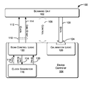
- FIG. 1 is a block diagram illustrating an image scanning device, according to some embodiments.
- FIG. 2 is a plot of the dithered frequency of a clock signal as a function of time, according to some embodiments.
- FIG. 3 includes plots of the dithered frequency of a clock signal as a function of time for various dither phases, according to some embodiments.
- FIGS. 4-8 are flow diagrams of processes of synchronizing scan passes with dither cycles, according to some embodiments.
- Image scanners typically use a scanning mechanism in which a sensor or sensor array is sequentially moved or passed over adjacent lines of a source image. As the sensor moves across the source image, the sensor transmits a serial sequence of scanned color and/or brightness values. The values are sampled and transmitted at a relatively high frequency.
- sensors may be sensitive to variable scanning frequencies. For example, some sensors may have outputs that decay or settle with time, and some designs may sample such outputs before the outputs have completely settled. For at least these reasons, even small variations of scanning and data transfer rates may produce undesirable effects such as inconsistencies, anomalies, and artifacts in scanned image data. Accordingly, it may be beneficial to sample the outputs of image sensors at consistent rates to avoid such effects.
- an image scanner may use clock dithering, which is an intentional variation of scanning and data transfer rates, to reduce EMI emissions.
- Embodiments described herein include methods and apparatuses for implementing clock dithering while avoiding the undesirable effects caused by variations of scanning and data transfer rates, as described above.
- all scan passes of a page of a document being scanned are started at the same phase of a dither cycle.
- all scan passes may be started at zero offset of a dither cycle.
- scan results for all the scan passes will experience identical dither configurations, thus avoiding variations of scanning and data transfer rates among the multiple scan passes of a page of a document.
- each scanning pass commences at the same point within a dithering cycle, and each scanning pass is thus performed under a consistent and repeatable clock frequency pattern.
- Such configurations may comprise several full dither cycles plus a partial dither cycle, for example.
- example embodiments involve scanning processes
- techniques described herein may be implemented involving laser scanning by a printer.
- issues and/or artifacts described for scanning by a scanner may be the same as or similar to those for scanning by a printer.
- Differences between scanning by a scanner and scanning by a printer may include direction of data and/or control.
- FIG. 1 is a block diagram illustrating an image scanning device 100 , according to some embodiments.
- Image scanning device 100 may be integrated with a printer mechanism and/or other components to form what has become commonly known as a multi-function printer or MFP (not illustrated).
- image scanning device 100 may comprise a stand-alone scanner.
- certain embodiments may comprise components or sub-components of image scanning device 100 .
- Image scanning device 100 may include a scanning unit 102 that performs image scanning functions.
- Scanning unit 102 has one or more optical sensors, sensor assemblies, or other scanning elements (not illustrated), which may comprise charge-coupled devices (CCDs) or other types of optical sensing devices.
- CCDs charge-coupled devices
- a source medium such as a sheet of paper, may contain a source image.
- the source medium may be positioned above, below, or otherwise adjacent to the scanning elements.
- the scanning elements may be configured to perform sequential scanning or sense passes over the source image.
- scanning unit 102 may have a transport mechanism (not illustrated) configured to move or pass the scanning elements across a horizontal line of the source medium so that the scanning elements or sensors can sample individual locations or pixels along the line.
- either the source medium or the transport mechanism of scanning unit 102 may be moved so that each pass of the scanning elements is of a different line of the source image.
- scanning unit 102 may perform scanning passes of sequential image lines, each line of which comprises multiple pixels. Within each line, data may be output from scanning unit 102 as a series or sequence of pixel values.
- the sequence of pixel values may correspond to physical movement of the scanning elements across the source medium, or may correspond to serial output characteristics of the scanning elements.
- Image scanning device 100 includes a device controller 104 that is configured to control the operation of scanning unit 102 and any other integrated functionality such as a printer component (not illustrated).
- Device controller 104 may also be configured to receive scanning data from scanning unit 102 and its scanning elements.
- Device controller 104 may also perform other functions, such as communicating with external devices and interacting with users.
- device controller 104 may be at some distance from scanning unit 102 .
- device controller 104 may be positioned at the bottom of image scanner 100 , and a communications bus or cable (not illustrated) may extend within image scanner 100 between device controller 104 and the scanning unit 102 .
- a communications bus or cable (not illustrated) may extend within image scanner 100 between device controller 104 and the scanning unit 102 .
- Such a cable may carry or convey multiple signals, including data and control signals. These signals may include scanned data signals, clock signals, synchronization signals, and so forth.
- the cable may convey scanned pixel data from the scanning elements to device controller 104 , in synchronization with a clock signal.
- the clock signal may be dithered to mitigate electromagnetic emission issues.
- Communications between device controller 104 and scanning unit 102 take place through a communications bus or cable, which may include a control bus 106 and a data bus 108 .
- the communications cable may also include various timing and synchronization signals 110 .
- the timing and synchronization signals 110 may include a derivative clock signal 112 and a line start signal 114 , which will be referred to herein as the CLK/n signal and the LINE START signal, respectively.
- the CLK/n and LINE START signals may be considered part of the control bus, although the CLK/n and LINE START signals are shown separately for purposes of explanation.
- Scanning unit 102 may receive the CLK/n signal and the LINE START signal. Scanning unit 102 is responsive to the CLK/n and LINE START signals, as well as to other commands that may be presented through the control bus, to initiate individual sensing or scanning passes.
- Device controller 104 includes a clock generator module 116 that generates additional synchronization signals, including a CLK signal 118 and a SYNC signal 120 .
- Device controller 104 may also include a scan control logic module 122 that receives the CLK and SYNC signals and that generates the CLK/n and LINE START signals based on the CLK and SYNC signals.
- Device controller 104 includes a pixel data receive port 124 configured to receive serial pixel data transmitted by scanning unit 102 over data bus 108 .
- the serial pixel data may be in analog or digital format.
- An analog-to-digital converter (not illustrated) may be used within device controller 104 or scanning unit 102 to convert analog pixel data to digital pixel data.
- Device controller 104 may also include calibration logic module 126 that is configured to correct pixel data received from scanning unit 102 .
- Calibration logic module 222 may have access to correction data that is applied to received pixel values.
- the correction data may be obtained during a previous calibration procedure, in which a known calibration image is scanned and evaluated.
- the calibration image may have lines or areas of constant color and/or brightness, so that the consistency of scanning unit 102 may be evaluated at different physical locations relative to the source media. Sensed inconsistencies in different physical locations are noted, and correction values may be calculated corresponding to different pixel locations. During subsequent scanning of source media, the correction values may be applied to received pixel values based on the locations to which the pixel values correspond.
- Inconsistencies in pixel data may result from a variety of factors, such as variations in illumination, sensor positioning, and so forth. Calibration logic module 126 may assume that such inconsistencies are functions of position, and that such positional inconsistencies will remain relatively constant over time.
- the correction data may include correction values for each pixel position of a line, and each received line may be subject to the same correctional data.
- the correction data may have values corresponding to the respective pixel positions of an entire scanned sheet or two-dimensional scanned area.
- clock generator module 116 may receive a line start signal from scan control logic module 122 to start a dithering sequence.
- Sync signal 120 need not be present.
- phase determination may be performed by clock generator module 116 .
- clock generator module 116 may modify how it behaves based, at least in part, on receiving a line start signal from scan control logic module 122 .
- Clock generator module 116 may also modify how it behaves based, at least in part, on when clock generator module 116 receives a line start signal (relative to the dithering cycle).
- FIG. 2 is a plot 200 of the dithered frequency of a dithered clock signal 202 as a function of time, according to some embodiments.
- a clock signal may be generated by a clock generator such as 116 , illustrated in FIG. 1 .
- scan control logic module 122 may modulate the clock signal to generate dithered clock signal 202 .
- Clock signal 202 may be an oscillating signal having a nominal frequency that is dithered by some predefined amount such as by ⁇ 0.5-5% of the nominal frequency, with 3% being a typical dithering amount.
- the dither frequency is typically 30-100 KHz, but is not limited to this range.
- the dither period is less than or equal to the time required for a single scan pass.
- the dither period is shorter than the scan pass, and multiple dithering cycles may occur during every scan pass.
- Dithered clock signal 202 may have an upper frequency Fmax, a lower frequency Fmin, and a central frequency Fcenter.
- the frequency difference 204 between Fmax and Fmin may be about 10% of the nominal frequency, as mentioned above.
- the frequency offset at a particular phase of dithered clock signal 202 is considered to be the difference between the frequency at the particular phase and Fcenter.
- the largest frequency offset at phase 206 is Fmax and the frequency offset at phase 208 is Fmin.
- Fcenter need not be halfway between Fmin and Fmax (e.g., half of peak-to-peak range 204 ).
- dithered clock signal 202 varies as a triangle wave, but in other embodiments dithered clock signal 202 may vary as a sinusoidal wave, a sawtooth wave, or as any other time-varying function, for example.
- a dither cycle may be identified as a complete cycle of dithered clock signal 202 . For example, if the commencing of a dither cycle occurs at a particular phase of dithered clock signal 202 , then the end of the dither cycle occurs at the next occurrence of the particular phase. In the particular example embodiment illustrated in FIG. 2 , the dither cycle commences and ends at the phase of dithered clock signal 202 corresponding to the frequency Fcenter with positive slope.
- Ph 0 is considered to be the first quarter of the dither cycle
- Ph 1 is considered to be the second quarter of the dither cycle
- Ph 2 is considered to be the third quarter of the dither cycle
- Ph 3 is considered to be the fourth quarter of the dither cycle.
- FIG. 3 includes plots 302 - 310 of the dithered frequency of a clock signal 312 as a function of time for various dither phases at the time a trigger 314 is received or detected, according to some embodiments.
- the central frequency e.g., zero offset or Fcenter in FIG. 2
- the frequency of clock signal 202 is dithered as a triangle wave, but many types of frequency variations are possible.
- Trigger 314 may occur when a scan pass of one or more lines of a document commences.
- a subsequent trigger 316 may occur when a scan pass of the one or more lines of the document ends.
- Trigger 316 of a scan pass may be the same as the trigger for the next scan pass.
- Several complete dither cycles plus a partial dither cycle may occur during a scan pass.
- trigger 314 and trigger 316 of a scan pass may occur at any phase or portion of clock signal 312 . Examples of such cases are illustrated in plots 302 - 310 .
- trigger 314 occurs at a phase of clock signal 312 that corresponds to central frequency F 0 .
- trigger 314 occurs in the first quarter Ph 0 of clock signal 312 .
- trigger 314 occurs in the second quarter Ph 1 of clock signal 312 .
- trigger 314 occurs in the third quarter Ph 2 of clock signal 312 .
- trigger 314 occurs in the fourth quarter Ph 3 of clock signal 312 .
- dither configuration I corresponds to a “target” situation, where the duration of a single scan pass commences and ends at the same phase of clock signal 312 .
- trigger 314 and trigger 316 of the scan pass for configuration I both occur at zero frequency offset and the same phase of clock signal 312 .
- the scan pass includes complete dither cycles and a partial dither cycle 318 that ends at end trigger 316 .
- the initial scan pass e.g., a trigger of the scan pass
- techniques are performed so that the duration of each scan pass of a page of a document commences and ends at the same phase of clock signal 312 .
- Such techniques may include, for example, modifying the shape of the partial dither cycle based, at least in part, on the phase of the clock signal at which the trigger of the first scan pass of a page occurs. Subsequent scan passes of the page use the modified shape of the partial dither cycle.
- Plots 304 - 310 are examples of trigger 314 occurring at various phases of clock signal 312 , as described below.
- trigger 314 occurs at a phase 320 in the first quarter Ph 0 of clock signal 312 .
- This situation may correspond to a configuration II, which includes one or more complete dither cycles and a partial dither cycle 322 .
- Any of a number of techniques may be used to develop a dither configuration so that the duration of each scan pass of commences and ends at the same phase of clock signal 312 .
- a partial dither cycle a dither configuration may be modified as follows.
- a processor may detect or determine a phase difference 324 between the commencing 326 of a first scan pass of a document and phase 320 , which is the point of clock signal 312 where trigger 314 occurs.
- Partial dither cycle 322 may comprise a portion of a complete dither cycle corresponding to phase difference 324 plus a return-to-F 0 portion.
- the portion of a complete dither cycle corresponding to phase difference 324 is the portion of clock signal 312 between 328 and 330 and the return-to-F 0 portion is the portion of clock signal 312 between 330 and 332 .
- partial dither cycle 322 may also include a half dither cycle, which is the portion of partial dither cycle 322 above F 0 .
- the half dither cycle may be included so that partial dither cycle 322 ends at a particular desired phase which, in the example embodiments of FIG. 3 , corresponds to F 0 .
- clock dithering is suspended so that the frequency of clock signal 312 is not varied.
- duration 334 noise reduction benefits from dithering may be suppressed, but duration 334 is relatively short and any adverse effect caused by such suppression may be relatively small or negligible.
- the return-to-F 0 portion may be a linear transition of dither frequency, but any of a number of transition shapes may be used.
- configuration II of clock signal 312 ends at a particular phase (corresponding to zero-offset in the example embodiment of FIG. 3 ). All subsequent scan passes for a page of a document will commence at that particular phase. Thus, scan results for all the subsequent scan passes will experience identical dither configurations, thus avoiding variations of scanning and data transfer rates among the multiple scan passes of a page of a document.
- the process described above is performed for a first scan pass of a page of a document. Such a first scan pass may be repeated so that scan results of the first scan pass are replaced by scan results of the repeat scan pass.
- configuration II may be different for configurations III, IV, and V.
- any of a number of techniques may be used to render configuration I, which comprises a dithered clock signal 312 that commences at the same phase for all scan passes of a page of a document.
- trigger 314 occurs at a phase 336 in the second quarter Ph 1 of clock signal 312 .
- This situation may correspond to configuration III, which includes one or more complete dither cycles and a partial dither cycle 338 .
- a partial dither cycle may be modified as follows.
- a processor e.g., scan control logic module 122
- Partial dither cycle 338 may comprise a portion of a complete dither cycle plus a return-to-F 0 portion.
- clock dithering is suspended so that the frequency of clock signal 312 is not varied.
- duration 340 noise reduction benefits from dithering may be suppressed, but duration 340 is relatively short (though longer than 334 of configuration II) and any adverse effect caused by such suppression may be relatively small or negligible.
- the return-to-F 0 portion may be a linear transition of dither frequency, but any of a number of transition shapes may be used.
- configuration III of clock signal 312 ends at a particular phase (corresponding to zero-offset in the example embodiment of FIG. 3 ). All subsequent scan passes for a page of a document will commence at that particular phase. In other words, all subsequent scan passes may be performed accordingly to configuration I. Thus, scan results for all the subsequent scan passes will experience identical dither signatures, even though the commencing of the first scan pass occurred at an arbitrary phase (e.g., 336 ).
- trigger 314 occurs at a phase 342 in the third quarter Ph 2 of clock signal 312 .
- This situation may correspond to configuration IV, which includes one or more complete dither cycles and a partial dither cycle 344 .
- Partial dither cycle 344 may comprise a portion of a complete dither cycle plus a return-to-F 0 portion.
- Partial dither cycle 344 may include a half dither cycle, which is the portion of partial dither cycle 344 below F 0 .
- the half dither cycle may be included so that partial dither cycle 344 ends at a particular desired phase which, in the example embodiments of FIG. 3 , corresponds to F 0 .
- clock dithering is suspended so that the frequency of clock signal 312 is not varied.
- duration 346 noise reduction benefits from dithering may be suppressed, but duration 340 is relatively short and any adverse effect caused by such suppression may be relatively small or negligible.
- the return-to-F 0 portion may be a linear transition of dither frequency, but any of a number of transition shapes may be used.
- trigger 314 occurs at a phase 348 in the fourth quarter Ph 3 of clock signal 312 .
- This situation may correspond to configuration V, which includes one or more complete dither cycles and a partial dither cycle 350 .
- Partial dither cycle 350 may comprise a portion of a complete dither cycle plus a return-to-F 0 portion.
- clock dithering is suspended so that the frequency of clock signal 312 is not varied.
- duration 352 noise reduction benefits from dithering may be suppressed, but duration 352 is relatively short and any adverse effect caused by such suppression may be relatively small or negligible.
- the return-to-F 0 portion may be a linear transition of dither frequency, but any of a number of transition shapes may be used.
- FIG. 4 is a flow diagram of a process 400 for synchronizing scan passes of a document with dither cycles, according to some embodiments. Such a process may be performed by scan control logic module 122 of image scanning device 100 illustrated in FIG. 1 , for example.
- Each of the blocks 402 , 404 , and 406 are illustrated in detail in FIGS. 5-7 and further described below.
- Block 402 includes an initial synchronization phase, which includes the first scan pass of a page of the document.
- Block 402 leads to development of a particular dither configuration (e.g., configuration I, illustrated in FIG. 3 ) that will be used for all subsequent scan passes of a particular page of the document.
- a particular dither configuration e.g., configuration I, illustrated in FIG. 3
- Block 404 includes a standard scan pass, which involves using the particular dither configuration generated in block 402 for all scan passes on the page of the document.
- Block 406 involves detecting the end of the page of the document. If the end of the page is detected (e.g., a timeout occurs), then process 400 returns to block 402 . If the end of the page is not detected (e.g., no timeout occurs), then process 400 returns to block 404 . Details of blocks 402 - 406 are now described with references to FIGS. 5-7 .
- FIG. 5 illustrates details of block 402 in flow diagram 400 .
- Block 402 comprises an initial synchronization phase, which may be the first scan pass of a page of a document.
- control logic module 122 of image scanning device 100 may dither a clock signal generated by clock generator module 116 , for example.
- control logic module 122 may determine if an initial trigger for a scan pass is detected. If not, then the process of block 402 returns to block 502 and dithering continues. On the other hand, if an initial trigger is detected, then the process proceeds to diamond 506 , where control logic module 122 may determine the portion of the clock signal, or the phase of the clock signal, at which the initial trigger occurred. For example, referring to FIG.
- a dithered clock signal (e.g., such as 202 ) may include a first quarter portion Ph 0 , a second quarter portion Ph 1 , a third quarter portion Ph 2 , and a fourth quarter portion Ph 3 .
- the process proceeds to block 508 and a configuration A will be developed and used for subsequent scan passes. If the initial trigger occurs in portion Ph 2 or Ph 3 of the clock signal, the process proceeds to block 510 and a configuration B will be developed and used for subsequent scan passes.
- the process proceeds from diamond 506 to block 508 .
- the frequency of the clock signal may be varied for several full dither cycles.
- the process proceeds to block 512 , where a partial dither cycle is developed for a configuration A.
- configuration A may be the same as or similar to configurations II and III, illustrated in FIG. 3 .
- the partial dither cycle is completed at block 514 where control logic module may linearly vary the frequency of the clock cycle to return to zero offset from the frequency of the non-dithered clock signal (e.g., Fcenter).
- the partial dither cycle may include a linear return to another frequency of the dithered clock signal. Whatever the final frequency of the linear return, this is the frequency at which all subsequent scan passes of a page of a document commence.
- the return to zero (or the return to another frequency) need not be linear. For example, a return to zero may follow an exponential decay or sinusoid.
- the process proceeds to block 404 , illustrated in FIG. 6 .
- the process proceeds from diamond 506 to block 510 .
- the frequency of the clock signal may be varied for several full dither cycles.
- the process proceeds to block 516 , where a partial dither cycle is developed for a configuration B.
- configuration B may be the same as or similar to configurations IV and V, illustrated in FIG. 3 .
- the partial dither cycle is completed at block 518 where control logic module may linearly vary the frequency of the clock cycle to return to zero-offset from the frequency of the non-dithered clock signal (e.g., Fcenter).
- the partial dither cycle may include a linear return to another frequency of the dithered clock signal. Whatever the final frequency of the linear return, this is the frequency at which all subsequent scan passes of a page of a document commence.
- the return to zero (or the return to another frequency) need not be linear. For example, a return to zero may follow an exponential decay or sinusoid.
- the process proceeds to block 404 , illustrated in FIG. 6 .
- FIG. 6 illustrates details of block 404 in flow diagram 400 .
- the first scan pass of a page may be repeated (the initial first scan pass having occurred during the process of block 402 ) using the clock signal configuration developed in block 402 .
- all the subsequent scan passes of the page will use the same clock signal configuration.
- a scan pass commences upon detection of an initial trigger (e.g., 314 ).
- the scan pass is performed during several full dither cycles.
- control logic module 122 may perform a partial dither cycle according to the clock signal configuration developed in block 402 .
- the partial dither cycle is completed at block 606 , where the control logic module 122 linearly returns the dither frequency to zero-offset from the frequency of the non-dithered clock signal (e.g., Fcenter).
- the partial dither cycle may include a linear return to another frequency of the dithered clock signal. Whatever the final frequency of the linear return, this is the frequency at which all scan passes of a page of a document commence.
- the return to zero (or the return to another frequency) need not be linear. For example, a return to zero may follow an exponential decay or sinusoid.
- the process proceeds to block 406 , illustrated in FIG. 7 .
- Block 406 is performed at the conclusion of each scan pass of the document.
- Block 406 includes a portion of process 400 where a last scan pass of a page may be detected.
- control logic module 122 at the end of the clock signal configuration developed in block 402 , waits for a trigger of a subsequent scan pass. Such waiting may occur over a duration when dithering is suppressed and the frequency of the clock signal is held constant (e.g., refer to durations 334 , 340 , 346 , and 352 illustrated in FIG. 3 ).
- control logic module 122 may determine if a timeout signal is detected.
- Such a time-out signal may be generated by image scanning device 100 to indicate that the end of a page is encountered and the last scan pass is the final scan pass for the page. If a timeout signal is not detected, then process 400 returns to block 404 so that control logic module 122 may perform additional one or more scan passes. If a timeout signal is detected, then process 400 returns to block 402 so that control logic module 122 may generate a new clock signal configuration for a subsequent page.
- FIG. 8 is a flow diagram of a process 800 for reducing electromagnetic emissions by an image scanner by synchronizing scan passes with dither cycles, according to some embodiments.
- Process 800 may be performed while scanning a page of a document.
- Process 800 which may be performed by a processor such as control logic module 122 , may be the same as or similar to process 400 described above.
- the processor may cyclically dither a frequency of a clock signal of the image scanner by repeated dither cycles.
- An example of a dither cycle is illustrated in FIG. 2 .
- configuration I of FIG. 3 illustrates three full dither cycles.
- the processor may determine a phase of the dither cycle when a scan pass of the page commences.
- the scan pass commences upon detection of an initial trigger, such as 314 illustrated in FIG. 3 .
- the processor may commence all subsequent scan passes of the page at a particular phase shift from the determined phase. For example, all scan passes of the page may commence at a phase of the clock signal corresponding to the non-dithered frequency of the clock signal. For example, if the determined phase is 90 degrees (out of a 360 degree dither cycle) from the zero-offset frequency of the clock signal, then all scan passes may commence at a phase shift of 90 degrees from the determined phase, which is at the zero frequency offset of the dither cycle.
- the processor may commence all subsequent scan passes of the page of the document at the particular phase shift from the determined phase without delaying the subsequent scan passes.
- the processor may detect the last scan pass and subsequently determine a phase of the dither cycle when the first scan pass of the next page of the document commences. Following process 800 , the processor may then commence all subsequent scan passes of the subsequent page of the document at a particular phase shift from the determined second phase.
- an article of manufacture may be provided that includes a storage medium having instructions stored thereon that, if executed, result in the operations described above.
- the storage medium comprises some type of non-transitory memory (not shown).
- the article of manufacture may be a computer-readable medium such as, for example, software or firmware.
- module may refer to, be part of, or include an Application Specific Integrated Circuit (ASIC), an electronic circuit, a processor (shared, dedicated, or group) and/or memory (shared, dedicated, or group) that execute one or more software or firmware programs, a combinational logic circuit, and/or other suitable components that provide the described functionality.
- ASIC Application Specific Integrated Circuit
- processor shared, dedicated, or group
- memory shared, dedicated, or group
- the logic and functionality described herein may be implemented by any such components.
Landscapes
- Engineering & Computer Science (AREA)
- Multimedia (AREA)
- Signal Processing (AREA)
- Physics & Mathematics (AREA)
- Electromagnetism (AREA)
- Environmental & Geological Engineering (AREA)
- Facsimile Scanning Arrangements (AREA)
Abstract
Description
Claims (21)
Priority Applications (1)
| Application Number | Priority Date | Filing Date | Title |
|---|---|---|---|
| US14/659,320 US9444964B1 (en) | 2014-03-17 | 2015-03-16 | Method and apparatus for scanning an image |
Applications Claiming Priority (2)
| Application Number | Priority Date | Filing Date | Title |
|---|---|---|---|
| US201461954480P | 2014-03-17 | 2014-03-17 | |
| US14/659,320 US9444964B1 (en) | 2014-03-17 | 2015-03-16 | Method and apparatus for scanning an image |
Publications (1)
| Publication Number | Publication Date |
|---|---|
| US9444964B1 true US9444964B1 (en) | 2016-09-13 |
Family
ID=56881508
Family Applications (1)
| Application Number | Title | Priority Date | Filing Date |
|---|---|---|---|
| US14/659,320 Expired - Fee Related US9444964B1 (en) | 2014-03-17 | 2015-03-16 | Method and apparatus for scanning an image |
Country Status (1)
| Country | Link |
|---|---|
| US (1) | US9444964B1 (en) |
Citations (20)
| Publication number | Priority date | Publication date | Assignee | Title |
|---|---|---|---|---|
| US4757389A (en) | 1987-06-15 | 1988-07-12 | Xerox Corporation | Calibration improvement with dither for a raster input scanner |
| US5193013A (en) | 1990-05-29 | 1993-03-09 | Olive Tree Technology, Inc. | Scanner with non-linearity compensating pixel clock |
| JP2000022959A (en) | 1998-07-03 | 2000-01-21 | Canon Inc | Image forming device and its clock control method |
| JP2001077989A (en) | 1999-09-03 | 2001-03-23 | Canon Inc | Image-forming device, and method therefor, and computer- readable storage medium |
| JP2001268355A (en) | 2000-03-21 | 2001-09-28 | Ricoh Co Ltd | Image scanning apparatus |
| US20010032323A1 (en) * | 2000-04-06 | 2001-10-18 | Konica Corporation | Clock generating device |
| JP2002281252A (en) | 2001-03-16 | 2002-09-27 | Ricoh Co Ltd | Image processing system and image forming system |
| CN1386377A (en) | 2000-07-28 | 2002-12-18 | 皇家菲利浦电子有限公司 | Method and apparatus for spread spectrum clocking of digital video |
| JP2003008845A (en) | 2001-06-20 | 2003-01-10 | Ricoh Co Ltd | Image processor |
| US20060238225A1 (en) | 2004-07-30 | 2006-10-26 | Keithley Douglas G | Variable frequency generator |
| CN1972365A (en) | 2005-11-25 | 2007-05-30 | 夏普株式会社 | Image processing apparatus, image reading apparatus, and image forming apparatus |
| US20080106748A1 (en) * | 2006-11-02 | 2008-05-08 | Hajime Tsukahara | Image reading apparatus and image forming apparatus including the image reading apparatus |
| US20090086045A1 (en) | 2007-09-28 | 2009-04-02 | James Giebel | Method and System for a Configurable Communications Interface |
| US20090140896A1 (en) * | 2007-11-23 | 2009-06-04 | Stmicroelectronics S.R.L. | Clock dithering process for reducing electromagnetic interference in d/a converters and apparatus for carrying out such process |
| JP2009141523A (en) | 2007-12-04 | 2009-06-25 | Canon Inc | Device and method for reading image |
| EP2088766A1 (en) | 2008-02-06 | 2009-08-12 | Sony Corporation | Solid-state image pickup device |
| US20090213261A1 (en) | 2008-02-27 | 2009-08-27 | Nagase Masaki | Timing generator and image scanning apparatus |
| EP2150041A2 (en) | 2008-07-29 | 2010-02-03 | Ricoh Company, Limited | Image reading device and image forming apparatus |
| US20100193588A1 (en) | 2009-02-04 | 2010-08-05 | Datalogic Scanning, Inc. | Systems and methods for selectively masking a scan volume of a data reader |
| US20120099159A1 (en) * | 2010-10-26 | 2012-04-26 | Keithley Douglas G | Dither-synchronized image scanning |
-
2015
- 2015-03-16 US US14/659,320 patent/US9444964B1/en not_active Expired - Fee Related
Patent Citations (24)
| Publication number | Priority date | Publication date | Assignee | Title |
|---|---|---|---|---|
| US4757389A (en) | 1987-06-15 | 1988-07-12 | Xerox Corporation | Calibration improvement with dither for a raster input scanner |
| US5193013A (en) | 1990-05-29 | 1993-03-09 | Olive Tree Technology, Inc. | Scanner with non-linearity compensating pixel clock |
| JP2000022959A (en) | 1998-07-03 | 2000-01-21 | Canon Inc | Image forming device and its clock control method |
| JP2001077989A (en) | 1999-09-03 | 2001-03-23 | Canon Inc | Image-forming device, and method therefor, and computer- readable storage medium |
| JP2001268355A (en) | 2000-03-21 | 2001-09-28 | Ricoh Co Ltd | Image scanning apparatus |
| US20010032323A1 (en) * | 2000-04-06 | 2001-10-18 | Konica Corporation | Clock generating device |
| CN1386377A (en) | 2000-07-28 | 2002-12-18 | 皇家菲利浦电子有限公司 | Method and apparatus for spread spectrum clocking of digital video |
| US6665019B1 (en) | 2000-07-28 | 2003-12-16 | Koninklijke Philips Electronics N.V. | Method and apparatus for spread spectrum clocking of digital video |
| JP2002281252A (en) | 2001-03-16 | 2002-09-27 | Ricoh Co Ltd | Image processing system and image forming system |
| US20040013321A1 (en) | 2001-03-16 | 2004-01-22 | Satoshi Ohkawa | Method and apparatus for image processing with an effective line noise correction |
| JP2003008845A (en) | 2001-06-20 | 2003-01-10 | Ricoh Co Ltd | Image processor |
| US20060238225A1 (en) | 2004-07-30 | 2006-10-26 | Keithley Douglas G | Variable frequency generator |
| CN1972365A (en) | 2005-11-25 | 2007-05-30 | 夏普株式会社 | Image processing apparatus, image reading apparatus, and image forming apparatus |
| US20070120989A1 (en) | 2005-11-25 | 2007-05-31 | Takahiro Minami | Image processing apparatus, image reading apparatus, and image forming apparatus |
| US20080106748A1 (en) * | 2006-11-02 | 2008-05-08 | Hajime Tsukahara | Image reading apparatus and image forming apparatus including the image reading apparatus |
| US20090086045A1 (en) | 2007-09-28 | 2009-04-02 | James Giebel | Method and System for a Configurable Communications Interface |
| US20090140896A1 (en) * | 2007-11-23 | 2009-06-04 | Stmicroelectronics S.R.L. | Clock dithering process for reducing electromagnetic interference in d/a converters and apparatus for carrying out such process |
| JP2009141523A (en) | 2007-12-04 | 2009-06-25 | Canon Inc | Device and method for reading image |
| EP2088766A1 (en) | 2008-02-06 | 2009-08-12 | Sony Corporation | Solid-state image pickup device |
| CN101567641A (en) | 2008-02-06 | 2009-10-28 | 索尼株式会社 | Solid-state image pickup device |
| US20090213261A1 (en) | 2008-02-27 | 2009-08-27 | Nagase Masaki | Timing generator and image scanning apparatus |
| EP2150041A2 (en) | 2008-07-29 | 2010-02-03 | Ricoh Company, Limited | Image reading device and image forming apparatus |
| US20100193588A1 (en) | 2009-02-04 | 2010-08-05 | Datalogic Scanning, Inc. | Systems and methods for selectively masking a scan volume of a data reader |
| US20120099159A1 (en) * | 2010-10-26 | 2012-04-26 | Keithley Douglas G | Dither-synchronized image scanning |
Non-Patent Citations (1)
| Title |
|---|
| The PCT Search Report mailed Jan. 20, 2012 for PCT application No. PCT/US11/56561, 9 pages. |
Similar Documents
| Publication | Publication Date | Title |
|---|---|---|
| JP6111606B2 (en) | Drive control device, drive control method, and video output device | |
| US9813068B2 (en) | Spread spectrum clock generator, electronic apparatus, and spread spectrum clock generation method | |
| JP4816781B2 (en) | Spread spectrum clock frequency level detection method and spread spectrum clock frequency level detection apparatus | |
| US8861041B2 (en) | Image reading device provided with a spread spectrum clock generator and correction waveform data and an image forming apparatus comprising the image reading device | |
| EP3799409A1 (en) | Signal correction device, image reading device, image processing apparatus, signal correction method, and computer program product | |
| JP5257089B2 (en) | Image reading apparatus and image forming apparatus | |
| US8976417B2 (en) | Dither-synchronized image scanning | |
| US9444964B1 (en) | Method and apparatus for scanning an image | |
| US8471886B2 (en) | Image forming apparatus and control method | |
| JP2013546251A5 (en) | Method of reducing the electromagnetic radiation of an image scanner, an optical scanner and an apparatus for reducing the electromagnetic radiation | |
| JP2000224392A (en) | Image pickup device and method and storage medium read by computer | |
| JP2011160084A (en) | Clock output method, clock output circuit, and image forming apparatus | |
| JP2018088568A (en) | Image processing device | |
| KR101235223B1 (en) | Image forming apparatus and method for generating output signal thereof | |
| JP6150618B2 (en) | Image processing apparatus and data transfer method | |
| US20140168693A1 (en) | Printing apparatus and control method thereof, image processing apparatus, image processing method, and non-transitory computer-readable medium | |
| JP5724247B2 (en) | Image reading apparatus and image reading method | |
| JP2009267793A (en) | Video signal processor | |
| JP2011166675A (en) | Image reader and image read control method | |
| JP2002152016A (en) | Circuit with clock-up function and image reader using it | |
| JP6042672B2 (en) | Image reading device | |
| TW202305560A (en) | Pen signal detection method, sensor controller, and position detection system | |
| CN115882323A (en) | Laser scanning correction method and device | |
| JP2017152944A (en) | Image processing apparatus | |
| JP2012249272A (en) | Image reading device and image forming device |
Legal Events
| Date | Code | Title | Description |
|---|---|---|---|
| AS | Assignment |
Owner name: LEXMARK INTERNATIONAL, INC., KENTUCKY Free format text: ASSIGNMENT OF ASSIGNORS INTEREST;ASSIGNORS:FISTER, ZACHARY NATHAN;HARDIN, KEITH BRYAN;THOMPSON, KARL MARK;AND OTHERS;SIGNING DATES FROM 20150806 TO 20150807;REEL/FRAME:036280/0549 |
|
| AS | Assignment |
Owner name: MARVELL SEMICONDUCTOR, INC.,, CALIFORNIA Free format text: ASSIGNMENT OF ASSIGNORS INTEREST;ASSIGNORS:FORMAL, BENNETT;KEITHLEY, DOUGLAS GENE;REEL/FRAME:036291/0979 Effective date: 20150302 Owner name: MARVELL INTERNATIONAL LTD., BERMUDA Free format text: ASSIGNMENT OF ASSIGNORS INTEREST;ASSIGNOR:MARVELL SEMICONDUCTOR, INC.;REEL/FRAME:036292/0041 Effective date: 20150803 |
|
| STCF | Information on status: patent grant |
Free format text: PATENTED CASE |
|
| AS | Assignment |
Owner name: CHINA CITIC BANK CORPORATION LIMITED, GUANGZHOU BR Free format text: PATENT SECURITY AGREEMENT;ASSIGNOR:LEXMARK INTERNATIONAL, INC.;REEL/FRAME:046989/0396 Effective date: 20180402 |
|
| AS | Assignment |
Owner name: CHINA CITIC BANK CORPORATION LIMITED, GUANGZHOU BR Free format text: CORRECTIVE ASSIGNMENT TO CORRECT THE INCORRECT U.S. PATENT NUMBER PREVIOUSLY RECORDED AT REEL: 046989 FRAME: 0396. ASSIGNOR(S) HEREBY CONFIRMS THE PATENT SECURITY AGREEMENT;ASSIGNOR:LEXMARK INTERNATIONAL, INC.;REEL/FRAME:047760/0795 Effective date: 20180402 |
|
| AS | Assignment |
Owner name: CAVIUM INTERNATIONAL, CAYMAN ISLANDS Free format text: ASSIGNMENT OF ASSIGNORS INTEREST;ASSIGNOR:MARVELL INTERNATIONAL LTD.;REEL/FRAME:052918/0001 Effective date: 20191231 |
|
| FEPP | Fee payment procedure |
Free format text: MAINTENANCE FEE REMINDER MAILED (ORIGINAL EVENT CODE: REM.); ENTITY STATUS OF PATENT OWNER: LARGE ENTITY |
|
| AS | Assignment |
Owner name: MARVELL ASIA PTE, LTD., SINGAPORE Free format text: ASSIGNMENT OF ASSIGNORS INTEREST;ASSIGNOR:CAVIUM INTERNATIONAL;REEL/FRAME:053475/0001 Effective date: 20191231 |
|
| LAPS | Lapse for failure to pay maintenance fees |
Free format text: PATENT EXPIRED FOR FAILURE TO PAY MAINTENANCE FEES (ORIGINAL EVENT CODE: EXP.); ENTITY STATUS OF PATENT OWNER: LARGE ENTITY |
|
| STCH | Information on status: patent discontinuation |
Free format text: PATENT EXPIRED DUE TO NONPAYMENT OF MAINTENANCE FEES UNDER 37 CFR 1.362 |
|
| FP | Lapsed due to failure to pay maintenance fee |
Effective date: 20200913 |
|
| AS | Assignment |
Owner name: LEXMARK INTERNATIONAL, INC., KENTUCKY Free format text: RELEASE BY SECURED PARTY;ASSIGNOR:CHINA CITIC BANK CORPORATION LIMITED, GUANGZHOU BRANCH, AS COLLATERAL AGENT;REEL/FRAME:066345/0026 Effective date: 20220713 |