US9407066B2 - III-V lasers with integrated silicon photonic circuits - Google Patents
III-V lasers with integrated silicon photonic circuits Download PDFInfo
- Publication number
- US9407066B2 US9407066B2 US13/949,973 US201313949973A US9407066B2 US 9407066 B2 US9407066 B2 US 9407066B2 US 201313949973 A US201313949973 A US 201313949973A US 9407066 B2 US9407066 B2 US 9407066B2
- Authority
- US
- United States
- Prior art keywords
- layer
- stack
- forming
- iii
- substrate
- Prior art date
- Legal status (The legal status is an assumption and is not a legal conclusion. Google has not performed a legal analysis and makes no representation as to the accuracy of the status listed.)
- Active, expires
Links
- XUIMIQQOPSSXEZ-UHFFFAOYSA-N Silicon Chemical compound [Si] XUIMIQQOPSSXEZ-UHFFFAOYSA-N 0.000 title abstract description 25
- 229910052710 silicon Inorganic materials 0.000 title abstract description 25
- 239000010703 silicon Substances 0.000 title abstract description 25
- 239000004065 semiconductor Substances 0.000 claims abstract description 57
- 238000000034 method Methods 0.000 claims abstract description 24
- 239000000758 substrate Substances 0.000 claims abstract description 22
- 238000005530 etching Methods 0.000 claims description 12
- 239000012811 non-conductive material Substances 0.000 claims description 12
- 239000012212 insulator Substances 0.000 claims description 11
- 238000000151 deposition Methods 0.000 claims description 10
- 229910052751 metal Inorganic materials 0.000 claims description 2
- 239000002184 metal Substances 0.000 claims description 2
- 239000000463 material Substances 0.000 description 27
- 239000013078 crystal Substances 0.000 description 8
- 230000007547 defect Effects 0.000 description 5
- 230000003287 optical effect Effects 0.000 description 5
- VYPSYNLAJGMNEJ-UHFFFAOYSA-N Silicium dioxide Chemical compound O=[Si]=O VYPSYNLAJGMNEJ-UHFFFAOYSA-N 0.000 description 4
- 239000002131 composite material Substances 0.000 description 3
- 150000001875 compounds Chemical class 0.000 description 3
- 239000003989 dielectric material Substances 0.000 description 3
- 238000004519 manufacturing process Methods 0.000 description 3
- 230000002269 spontaneous effect Effects 0.000 description 3
- 238000003860 storage Methods 0.000 description 3
- IJGRMHOSHXDMSA-UHFFFAOYSA-N Atomic nitrogen Chemical compound N#N IJGRMHOSHXDMSA-UHFFFAOYSA-N 0.000 description 2
- 230000003321 amplification Effects 0.000 description 2
- 239000007795 chemical reaction product Substances 0.000 description 2
- 238000010586 diagram Methods 0.000 description 2
- 230000000694 effects Effects 0.000 description 2
- 239000003574 free electron Substances 0.000 description 2
- 229910052732 germanium Inorganic materials 0.000 description 2
- GNPVGFCGXDBREM-UHFFFAOYSA-N germanium atom Chemical compound [Ge] GNPVGFCGXDBREM-UHFFFAOYSA-N 0.000 description 2
- 239000000203 mixture Substances 0.000 description 2
- 238000003199 nucleic acid amplification method Methods 0.000 description 2
- 230000000737 periodic effect Effects 0.000 description 2
- 239000000047 product Substances 0.000 description 2
- 235000012239 silicon dioxide Nutrition 0.000 description 2
- 239000000377 silicon dioxide Substances 0.000 description 2
- 229910015844 BCl3 Inorganic materials 0.000 description 1
- ZOXJGFHDIHLPTG-UHFFFAOYSA-N Boron Chemical compound [B] ZOXJGFHDIHLPTG-UHFFFAOYSA-N 0.000 description 1
- GYHNNYVSQQEPJS-UHFFFAOYSA-N Gallium Chemical compound [Ga] GYHNNYVSQQEPJS-UHFFFAOYSA-N 0.000 description 1
- 229910001218 Gallium arsenide Inorganic materials 0.000 description 1
- 229910052782 aluminium Inorganic materials 0.000 description 1
- XAGFODPZIPBFFR-UHFFFAOYSA-N aluminium Chemical compound [Al] XAGFODPZIPBFFR-UHFFFAOYSA-N 0.000 description 1
- 229910021417 amorphous silicon Inorganic materials 0.000 description 1
- 229910052787 antimony Inorganic materials 0.000 description 1
- WATWJIUSRGPENY-UHFFFAOYSA-N antimony atom Chemical compound [Sb] WATWJIUSRGPENY-UHFFFAOYSA-N 0.000 description 1
- 238000003491 array Methods 0.000 description 1
- 229910052785 arsenic Inorganic materials 0.000 description 1
- RQNWIZPPADIBDY-UHFFFAOYSA-N arsenic atom Chemical compound [As] RQNWIZPPADIBDY-UHFFFAOYSA-N 0.000 description 1
- QVGXLLKOCUKJST-UHFFFAOYSA-N atomic oxygen Chemical compound [O] QVGXLLKOCUKJST-UHFFFAOYSA-N 0.000 description 1
- 229910052796 boron Inorganic materials 0.000 description 1
- 239000000919 ceramic Substances 0.000 description 1
- 239000002800 charge carrier Substances 0.000 description 1
- 230000001427 coherent effect Effects 0.000 description 1
- PMHQVHHXPFUNSP-UHFFFAOYSA-M copper(1+);methylsulfanylmethane;bromide Chemical compound Br[Cu].CSC PMHQVHHXPFUNSP-UHFFFAOYSA-M 0.000 description 1
- 230000003247 decreasing effect Effects 0.000 description 1
- 229910052733 gallium Inorganic materials 0.000 description 1
- BHEPBYXIRTUNPN-UHFFFAOYSA-N hydridophosphorus(.) (triplet) Chemical compound [PH] BHEPBYXIRTUNPN-UHFFFAOYSA-N 0.000 description 1
- 229910052738 indium Inorganic materials 0.000 description 1
- APFVFJFRJDLVQX-UHFFFAOYSA-N indium atom Chemical compound [In] APFVFJFRJDLVQX-UHFFFAOYSA-N 0.000 description 1
- 230000010354 integration Effects 0.000 description 1
- 239000013067 intermediate product Substances 0.000 description 1
- 238000012986 modification Methods 0.000 description 1
- 230000004048 modification Effects 0.000 description 1
- 229910052757 nitrogen Inorganic materials 0.000 description 1
- 239000000615 nonconductor Substances 0.000 description 1
- 239000001301 oxygen Substances 0.000 description 1
- 229910052760 oxygen Inorganic materials 0.000 description 1
- 230000001902 propagating effect Effects 0.000 description 1
- 230000006798 recombination Effects 0.000 description 1
- 238000005215 recombination Methods 0.000 description 1
- 238000000926 separation method Methods 0.000 description 1
- 230000007704 transition Effects 0.000 description 1
- FAQYAMRNWDIXMY-UHFFFAOYSA-N trichloroborane Chemical compound ClB(Cl)Cl FAQYAMRNWDIXMY-UHFFFAOYSA-N 0.000 description 1
Images


Classifications
-
- H—ELECTRICITY
- H01—ELECTRIC ELEMENTS
- H01S—DEVICES USING THE PROCESS OF LIGHT AMPLIFICATION BY STIMULATED EMISSION OF RADIATION [LASER] TO AMPLIFY OR GENERATE LIGHT; DEVICES USING STIMULATED EMISSION OF ELECTROMAGNETIC RADIATION IN WAVE RANGES OTHER THAN OPTICAL
- H01S5/00—Semiconductor lasers
- H01S5/20—Structure or shape of the semiconductor body to guide the optical wave ; Confining structures perpendicular to the optical axis, e.g. index or gain guiding, stripe geometry, broad area lasers, gain tailoring, transverse or lateral reflectors, special cladding structures, MQW barrier reflection layers
- H01S5/22—Structure or shape of the semiconductor body to guide the optical wave ; Confining structures perpendicular to the optical axis, e.g. index or gain guiding, stripe geometry, broad area lasers, gain tailoring, transverse or lateral reflectors, special cladding structures, MQW barrier reflection layers having a ridge or stripe structure
- H01S5/227—Buried mesa structure ; Striped active layer
- H01S5/2275—Buried mesa structure ; Striped active layer mesa created by etching
-
- H—ELECTRICITY
- H01—ELECTRIC ELEMENTS
- H01S—DEVICES USING THE PROCESS OF LIGHT AMPLIFICATION BY STIMULATED EMISSION OF RADIATION [LASER] TO AMPLIFY OR GENERATE LIGHT; DEVICES USING STIMULATED EMISSION OF ELECTROMAGNETIC RADIATION IN WAVE RANGES OTHER THAN OPTICAL
- H01S3/00—Lasers, i.e. devices using stimulated emission of electromagnetic radiation in the infrared, visible or ultraviolet wave range
- H01S3/05—Construction or shape of optical resonators; Accommodation of active medium therein; Shape of active medium
- H01S3/06—Construction or shape of active medium
- H01S3/063—Waveguide lasers, i.e. whereby the dimensions of the waveguide are of the order of the light wavelength
- H01S3/0632—Thin film lasers in which light propagates in the plane of the thin film
- H01S3/0637—Integrated lateral waveguide, e.g. the active waveguide is integrated on a substrate made by Si on insulator technology (Si/SiO2)
-
- H—ELECTRICITY
- H01—ELECTRIC ELEMENTS
- H01S—DEVICES USING THE PROCESS OF LIGHT AMPLIFICATION BY STIMULATED EMISSION OF RADIATION [LASER] TO AMPLIFY OR GENERATE LIGHT; DEVICES USING STIMULATED EMISSION OF ELECTROMAGNETIC RADIATION IN WAVE RANGES OTHER THAN OPTICAL
- H01S3/00—Lasers, i.e. devices using stimulated emission of electromagnetic radiation in the infrared, visible or ultraviolet wave range
- H01S3/23—Arrangements of two or more lasers not provided for in groups H01S3/02 - H01S3/22, e.g. tandem arrangements of separate active media
- H01S3/2375—Hybrid lasers
-
- H—ELECTRICITY
- H01—ELECTRIC ELEMENTS
- H01S—DEVICES USING THE PROCESS OF LIGHT AMPLIFICATION BY STIMULATED EMISSION OF RADIATION [LASER] TO AMPLIFY OR GENERATE LIGHT; DEVICES USING STIMULATED EMISSION OF ELECTROMAGNETIC RADIATION IN WAVE RANGES OTHER THAN OPTICAL
- H01S5/00—Semiconductor lasers
- H01S5/02—Structural details or components not essential to laser action
- H01S5/026—Monolithically integrated components, e.g. waveguides, monitoring photo-detectors, drivers
-
- H—ELECTRICITY
- H01—ELECTRIC ELEMENTS
- H01S—DEVICES USING THE PROCESS OF LIGHT AMPLIFICATION BY STIMULATED EMISSION OF RADIATION [LASER] TO AMPLIFY OR GENERATE LIGHT; DEVICES USING STIMULATED EMISSION OF ELECTROMAGNETIC RADIATION IN WAVE RANGES OTHER THAN OPTICAL
- H01S5/00—Semiconductor lasers
- H01S5/10—Construction or shape of the optical resonator, e.g. extended or external cavity, coupled cavities, bent-guide, varying width, thickness or composition of the active region
- H01S5/1053—Comprising an active region having a varying composition or cross-section in a specific direction
- H01S5/1057—Comprising an active region having a varying composition or cross-section in a specific direction varying composition along the optical axis
-
- H—ELECTRICITY
- H01—ELECTRIC ELEMENTS
- H01S—DEVICES USING THE PROCESS OF LIGHT AMPLIFICATION BY STIMULATED EMISSION OF RADIATION [LASER] TO AMPLIFY OR GENERATE LIGHT; DEVICES USING STIMULATED EMISSION OF ELECTROMAGNETIC RADIATION IN WAVE RANGES OTHER THAN OPTICAL
- H01S5/00—Semiconductor lasers
- H01S5/10—Construction or shape of the optical resonator, e.g. extended or external cavity, coupled cavities, bent-guide, varying width, thickness or composition of the active region
- H01S5/16—Window-type lasers, i.e. with a region of non-absorbing material between the active region and the reflecting surface
- H01S5/166—Window-type lasers, i.e. with a region of non-absorbing material between the active region and the reflecting surface with window regions comprising non-semiconducting materials
-
- H—ELECTRICITY
- H01—ELECTRIC ELEMENTS
- H01S—DEVICES USING THE PROCESS OF LIGHT AMPLIFICATION BY STIMULATED EMISSION OF RADIATION [LASER] TO AMPLIFY OR GENERATE LIGHT; DEVICES USING STIMULATED EMISSION OF ELECTROMAGNETIC RADIATION IN WAVE RANGES OTHER THAN OPTICAL
- H01S5/00—Semiconductor lasers
- H01S5/20—Structure or shape of the semiconductor body to guide the optical wave ; Confining structures perpendicular to the optical axis, e.g. index or gain guiding, stripe geometry, broad area lasers, gain tailoring, transverse or lateral reflectors, special cladding structures, MQW barrier reflection layers
- H01S5/2004—Confining in the direction perpendicular to the layer structure
- H01S5/2018—Optical confinement, e.g. absorbing-, reflecting- or waveguide-layers
-
- H—ELECTRICITY
- H01—ELECTRIC ELEMENTS
- H01S—DEVICES USING THE PROCESS OF LIGHT AMPLIFICATION BY STIMULATED EMISSION OF RADIATION [LASER] TO AMPLIFY OR GENERATE LIGHT; DEVICES USING STIMULATED EMISSION OF ELECTROMAGNETIC RADIATION IN WAVE RANGES OTHER THAN OPTICAL
- H01S5/00—Semiconductor lasers
- H01S5/30—Structure or shape of the active region; Materials used for the active region
- H01S5/3013—AIIIBV compounds
-
- H—ELECTRICITY
- H01—ELECTRIC ELEMENTS
- H01S—DEVICES USING THE PROCESS OF LIGHT AMPLIFICATION BY STIMULATED EMISSION OF RADIATION [LASER] TO AMPLIFY OR GENERATE LIGHT; DEVICES USING STIMULATED EMISSION OF ELECTROMAGNETIC RADIATION IN WAVE RANGES OTHER THAN OPTICAL
- H01S5/00—Semiconductor lasers
- H01S5/02—Structural details or components not essential to laser action
- H01S5/0206—Substrates, e.g. growth, shape, material, removal or bonding
- H01S5/021—Silicon based substrates
-
- H—ELECTRICITY
- H01—ELECTRIC ELEMENTS
- H01S—DEVICES USING THE PROCESS OF LIGHT AMPLIFICATION BY STIMULATED EMISSION OF RADIATION [LASER] TO AMPLIFY OR GENERATE LIGHT; DEVICES USING STIMULATED EMISSION OF ELECTROMAGNETIC RADIATION IN WAVE RANGES OTHER THAN OPTICAL
- H01S5/00—Semiconductor lasers
- H01S5/10—Construction or shape of the optical resonator, e.g. extended or external cavity, coupled cavities, bent-guide, varying width, thickness or composition of the active region
- H01S5/1003—Waveguide having a modified shape along the axis, e.g. branched, curved, tapered, voids
- H01S5/1017—Waveguide having a void for insertion of materials to change optical properties
-
- H—ELECTRICITY
- H01—ELECTRIC ELEMENTS
- H01S—DEVICES USING THE PROCESS OF LIGHT AMPLIFICATION BY STIMULATED EMISSION OF RADIATION [LASER] TO AMPLIFY OR GENERATE LIGHT; DEVICES USING STIMULATED EMISSION OF ELECTROMAGNETIC RADIATION IN WAVE RANGES OTHER THAN OPTICAL
- H01S5/00—Semiconductor lasers
- H01S5/10—Construction or shape of the optical resonator, e.g. extended or external cavity, coupled cavities, bent-guide, varying width, thickness or composition of the active region
- H01S5/12—Construction or shape of the optical resonator, e.g. extended or external cavity, coupled cavities, bent-guide, varying width, thickness or composition of the active region the resonator having a periodic structure, e.g. in distributed feedback [DFB] lasers
- H01S5/125—Distributed Bragg reflector [DBR] lasers
Definitions
- the present invention relates to photonic integrated circuits and, more particularly, to integrating III-V lasers with silicon-based photonic structures.
- Photonic integrated circuits provide substantial benefits over conventional electronics.
- the use of photonics allows signals to propagate at the speed of light within the circuit, greatly increasing the potential speed of PIC devices.
- structures for silicon-based PICs exist, silicon lacks the ability to generate light by itself.
- III-V materials have been employed in conjunction with silicon by fusing a III-V light-emitting device to a silicon waveguide. This has been accomplished using a process called plasma-assisted wafer bonding, where the materials are exposed to an oxygen plasma before being pressed together.
- the direct growth of III-V materials on silicon generally results in crystal dislocations, defects which shorten the lifetime of the laser.
- discrete optical components will frequently be misaligned when fused together. Such misalignments between optical components introduce optical loss within PICs.
- a laser includes a three-layer semiconductor stack formed from III-V semiconductors on a substrate, wherein a middle layer has a lower bandgap than a top layer and a bottom layer; a mirror region monolithically formed at a first end of the stack, configured to reflect emitted light in the direction of the stack; and a waveguide region monolithically formed at a second end of the stack, configured to transmit emitted light.
- a laser includes a plurality of three-layer semiconductor stacks formed from III-V semiconductors on a substrate, wherein a middle layer has a lower bandgap than a top layer and a bottom layer and wherein the stack has a height-to-width aspect ratio greater than 1; a mirror region monolithically formed at a first end of the stacks, configured to reflect emitted light in the direction of the stacks, said mirror region comprising alternating regions of first and second non-conductive materials having different indices of refraction; a waveguide region monolithically formed from a non-conductive material at a second end of the stacks, configured to transmit emitted light; a front contact that provides a shared electrical connection to the top layer of the stacks; and a back contact comprising a conductive layer in the substrate that provides a shared electrical connection to the bottom layer of the stacks.
- a method for forming a laser includes etching a high-aspect ratio trench into an insulator layer on a substrate; depositing a three-layer semiconductor stack formed from III-V semiconductors on a substrate, wherein a middle layer has a lower bandgap than a top layer and a bottom layer; and monolithically forming a mirror region and a waveguide region in contact with respective ends of the stack.
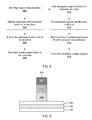
- FIG. 1 is a cross-sectional view of a step in forming a III-V laser with integrated silicon photonic circuits in accordance with the present principles
- FIG. 2 is a cross-sectional view of a step in forming a III-V laser with integrated silicon photonic circuits in accordance with the present principles
- FIG. 3 is a cross-sectional view of a step in forming a III-V laser with integrated silicon photonic circuits in accordance with the present principles
- FIG. 4 is a top-down view of a step in forming a III-V laser with integrated silicon photonic circuits in accordance with the present principles
- FIG. 5 is a top-down view of a step in forming a III-V laser with integrated silicon photonic circuits in accordance with the present principles
- FIG. 6 is a top-down view of a step in forming a III-V laser with integrated silicon photonic circuits in accordance with the present principles
- FIG. 7 is a top-down view of a step in forming a III-V laser with integrated silicon photonic circuits in accordance with the present principles
- FIG. 8 is a block/flow diagram of a method of forming a III-V laser with integrated silicon photonic circuits in accordance with one illustrative embodiment
- FIG. 9 is a cross-sectional view of a step in forming an alternative embodiment of a III-V laser with integrated silicon photonic circuits in accordance with the present principles.
- FIG. 10 is a cross-sectional view of a step in forming an alternative embodiment of a III-V laser with integrated silicon photonic circuits in accordance with the present principles.
- FIG. 11 is a top-down view of a step in forming an alternative embodiment of a III-V laser with integrated silicon photonic circuits in accordance with the present principles.
- Embodiments of the present principles provide III-V lasers that may be readily integrated with silicon photonic integrated circuits (PICs).
- PICs silicon photonic integrated circuits
- the present principles employ aspect ratio trapping (ART) to confine crystal defects when growing a monolithically integrated III-V/Si laser device.
- a p-type region may be formed with an n-type region.
- charge carriers move from one end of the diode toward the other, including free electrons and “holes.”
- holes When an electron meets a hole in an interface region, they may annihilate and produce a spontaneous emission.
- the electron assumes the energy state left open by the hole and emits energy having an energy that is the difference between the energy level of the free electron and of the hole. In a laser diode, this energy is released as light. Not all materials will produce light in these contexts—a “direct bandgap” material is needed.
- III-V materials While common single-element semiconductors, such as silicon and germanium, do not produce the needed effect, composite semiconductors such as III-V materials do. These materials include multiple layers of elements from the III group and the V group of the periodic table, respectively. The transition between the layers of the different materials creates the direct bandgap property that allows for spontaneous emission.
- spontaneous emissions may trigger additional, “stimulated” emissions by helping adjacent electrons and holes overcome a recombination energy. This produces an amplification effect, where a single photon can trigger multiple emissions. If there is more amplification than loss, the structure forms a laser and will continue to output light for as long as these conditions persist (e.g., as long as a voltage is applied).
- edge-emitting lasers deal specifically with edge-emitting lasers, though the present principles may be readily extended to other forms of laser.
- an edge-emitting laser diode a stack of semiconductor materials is used to generate coherent laser light.
- a layer of lower bandgap material is sandwiched between two layers of higher bandgap material.
- This structure is sometimes referred to as a double heterostructure laser, as the junction between each pair of layers is called a heterostructure.
- the general double heterostructure structure can be used and extended to form specific varieties of laser, such as quantum well lasers, quantum cascade lasers, distributed feedback lasers, etc. Those having ordinary skill in the art will recognize that the present principles may be applied to such structures.
- a challenge in forming heterostructure lasers is that the use of differing materials raises the potential for lattice mismatches.
- lattice mismatches can cause defects at the heterostructure and which can propagate through the structure, decreasing the efficiency and lifetime of the laser.
- a design for an integrated circuit chip of photovoltaic device may be created in a graphical computer programming language, and stored in a computer storage medium (such as a disk, tape, physical hard drive, or virtual hard drive such as in a storage access network). If the designer does not fabricate chips or the photolithographic masks used to fabricate chips, the designer may transmit the resulting design by physical means (e.g., by providing a copy of the storage medium storing the design) or electronically (e.g., through the Internet) to such entities, directly or indirectly.
- the stored design is then converted into the appropriate format (e.g., GDSII) for the fabrication of photolithographic masks, which typically include multiple copies of the chip design in question that are to be formed on a wafer.
- the photolithographic masks are utilized to define areas of the wafer (and/or the layers thereon) to be etched or otherwise processed.
- the resulting integrated circuit chips can be distributed by the fabricator in raw wafer form (that is, as a single wafer that has multiple unpackaged chips), as a bare die, or in a packaged form.
- the chip is mounted in a single chip package (such as a plastic carrier, with leads that are affixed to a motherboard or other higher level carrier) or in a multichip package (such as a ceramic carrier that has either or both surface interconnections or buried interconnections).
- the chip is then integrated with other chips, discrete circuit elements, and/or other signal processing devices as part of either (a) an intermediate product, such as a motherboard, or (b) an end product.
- the end product can be any product that includes integrated circuit chips, ranging from toys and other low-end applications to advanced computer products having a display, a keyboard or other input device, and a central processor.
- any of the following “/”, “and/or”, and “at least one of”, for example, in the cases of “A/B”, “A and/or B” and “at least one of A and B”, is intended to encompass the selection of the first listed option (A) only, or the selection of the second listed option (B) only, or the selection of both options (A and B).
- such phrasing is intended to encompass the selection of the first listed option (A) only, or the selection of the second listed option (B) only, or the selection of the third listed option (C) only, or the selection of the first and the second listed options (A and B) only, or the selection of the first and third listed options (A and C) only, or the selection of the second and third listed options (B and C) only, or the selection of all three options (A and B and C).
- This may be extended, as readily apparent by one of ordinary skill in this and related arts, for as many items listed.
- ART devices include arrays of tall dielectric trenches 102 with narrow openings 104 patterned on the substrate 106 .
- the “aspect ratio” refers specifically to the ratio between the height of the tranches 102 and width of the opening 104 .
- the aspect ratio should be larger than 1.
- Exemplary aspect ratios may range from, e.g., about 2 to about 5.
- the dielectric material is formed from, e.g., silicon dioxide and is on a silicon-on-insulator substrate formed from a semiconductor 106 , a buried insulator 108 formed from, e.g., silicon dioxide, on a bulk silicon substrate 110 .
- the semiconductor layer 106 may be a doped or metallized conductive layer formed from silicon, germanium, or another appropriate semiconductor material.
- a first multi-layer of semiconductor 202 is formed on the silicon layer 106
- a second multi-layer of semiconductor 204 is formed on top of the first semiconductor multi-layer 202
- a third multi-layer of semiconductor 206 is filled on top.
- the three semiconductor multi-layers 202 , 204 , and 206 are each III-V compound semiconductors formed from a composite of an element in the III-group of the periodic table and an element in the V-group.
- Such materials may include, e.g., boron, aluminum, gallium, or indium with nitrogen, phosphorous, arsenic, or antimony.
- the materials should be selected such that the multi-layers represented by second semiconductor 204 has the lowest III-V material bandgap compared to semiconductor multi-layers 202 and 206 .
- a chemical-mechanical planarization (CMP) may be performed to planarize the top of the third semiconductor multi-layer 206 with the top of the dielectric material 102 . It should be understood that, due to ART, crystal defects are confined to the bottom of the first semiconductor layer 202 .
- Ternary compositions such as those used in the III-V semiconductor stacks 304 of the present embodiments, allow for adjustment of the band gap within the range of the individual compounds.
- GaAs is limited to 850 nm, but Al(x)Ga(1 ⁇ x)As with an increased Al content increases the bandgap energy and thus produces a shorter emission wavelength.
- Quaternary and higher order compositions allow for adjustment of the band gap and the lattice constant, allowing increased radiant efficiency at a higher range of wavelengths.
- a lengthwise cut-away view of the ART trench 104 is shown.
- the ends of the trench 104 are etched to extend the trench around the semiconductor stack 304 , producing gaps 302 that extend down to the semiconductor layer 106 .
- the etch should be highly anisotropic to produce a strong ninety-degree joint between the exposed semiconductor layer 106 and the semiconductor stack 304 .
- Exemplary etches may include reactive-ion etches (RIEs) including, e.g., BCl 3 /Cl 2 and CH 4 /H 2 etches.
- RIEs reactive-ion etches
- a back contact region 402 is lithographically defined by etching away dielectric layer 102 down to the semiconductor layer 106 .
- the dielectric layer is further lithographically etched away at either end of the stacks 304 to clear away waveguide regions 404 . This etch removes material down to the buried dielectric layer 108 , removing the semiconductor layer 106 in the waveguide regions 404 .
- the back contact region 402 and the waveguide regions are filled with a non-conductive waveguide material 502 .
- the waveguide material can be, e.g., aluminum nitride, amorphous silicon, or amorphous III-V.
- One waveguide region 404 is patterned and etched to produce regularly spaced trenches. These trenches are filled with a second non-conductive material 602 that has a different refractive index from the first material 502 . This establishes a mirror region 604 .
- the separation of regions of second material 602 depends on the target wavelength of the laser and typically ranges from about 100 nm to about 1000 nm.
- FIG. 7 a top-down view of the semiconductor stacks 304 is shown.
- An opening is etched into back contact region 402 .
- a back contact 702 formed of multi-layers of metal is deposited in the etched portion and a front contact 704 is deposited across the semiconductor stacks 304 .
- the completed laser emits light from the ends of the stacks 304 .
- Light that is emitted in the direction of the mirror region 604 is reflected back and exits with the rest of the emitted light from the waveguide region 404 .
- the waveguide region 404 may be formed in contact with other optical features, allowing for monolithic integration of laser-generating components with passive optical components.
- the back contact 702 extends down to the semiconductor layer 106 .
- the semiconductor layer 106 may be a doped or metallized layer. Because each of the stacks 304 rests on the layer 106 , that layer that provides conductive connections between the back contact 702 and the individual stacks 304 .
- Block 802 etches high aspect ratio trenches 104 into an insulator layer 102 on a silicon-on-insulator substrate.
- Block 804 deposits a triple-layer semiconductor stack 304 formed from three III-V semiconductors 202 , 204 , and 206 , where the middle layer 204 has a lower bandgap than the first and third layers 202 and 206 .
- Block 806 creates space at the ends of the semiconductor stacks 304 using an anisotropic etch to remove insulator material down to the semiconductor layer 106 .
- Block 808 etches a back contact region connecting the stacks 304 and block 810 etches waveguide regions 404 starting at the previously-etched ends of the stacks 304 .
- lithographic etching may be used for blocks 808 and 810 .
- Block 812 fills in the waveguide regions 404 with a first non-conductor material 502 .
- Block 814 etches trenches in one waveguide region 404 and fills the trenches with a second non-conductive material 602 , forming mirror region 604 .
- Block 816 forms electrical contacts for the back contact 702 and the front contact 704 .
- FIG. 9 a lengthwise cut-away view of the stack 304 is shown in an alternative embodiment.
- This embodiment is a departure after block 806 .
- the remaining dielectric material 102 is removed using, e.g., a wet etch or other appropriate etching process, leaving the semiconductor layer 106 exposed.
- FIG. 10 a lengthwise cut-away view of the stack 304 is shown in an alternative embodiment.
- the semiconductor layer 106 around the stack 304 is selectively etched, leaving only the portion 1002 underneath the stack 304 and portions for the back contact.
- FIG. 11 a top-down view of the semiconductor stacks 304 in an alternative embodiment is shown.
- the dielectric layer 108 is exposed except for those regions 1102 of semiconductor material remaining to form the back contact region.
- the remaining regions 1102 of semiconductor material electrically connect the stacks 304 .
- the fabrication process resumes at block 812 , with the waveguide regions being defined by, e.g., lithographic processes.
Abstract
Description
Claims (13)
Priority Applications (2)
| Application Number | Priority Date | Filing Date | Title |
|---|---|---|---|
| US13/949,973 US9407066B2 (en) | 2013-07-24 | 2013-07-24 | III-V lasers with integrated silicon photonic circuits |
| US15/188,419 US9966735B2 (en) | 2013-07-24 | 2016-06-21 | III-V lasers with integrated silicon photonic circuits |
Applications Claiming Priority (1)
| Application Number | Priority Date | Filing Date | Title |
|---|---|---|---|
| US13/949,973 US9407066B2 (en) | 2013-07-24 | 2013-07-24 | III-V lasers with integrated silicon photonic circuits |
Related Child Applications (1)
| Application Number | Title | Priority Date | Filing Date |
|---|---|---|---|
| US15/188,419 Division US9966735B2 (en) | 2013-07-24 | 2016-06-21 | III-V lasers with integrated silicon photonic circuits |
Publications (2)
| Publication Number | Publication Date |
|---|---|
| US20150030047A1 US20150030047A1 (en) | 2015-01-29 |
| US9407066B2 true US9407066B2 (en) | 2016-08-02 |
Family
ID=52390509
Family Applications (2)
| Application Number | Title | Priority Date | Filing Date |
|---|---|---|---|
| US13/949,973 Active 2034-03-13 US9407066B2 (en) | 2013-07-24 | 2013-07-24 | III-V lasers with integrated silicon photonic circuits |
| US15/188,419 Active 2033-08-03 US9966735B2 (en) | 2013-07-24 | 2016-06-21 | III-V lasers with integrated silicon photonic circuits |
Family Applications After (1)
| Application Number | Title | Priority Date | Filing Date |
|---|---|---|---|
| US15/188,419 Active 2033-08-03 US9966735B2 (en) | 2013-07-24 | 2016-06-21 | III-V lasers with integrated silicon photonic circuits |
Country Status (1)
| Country | Link |
|---|---|
| US (2) | US9407066B2 (en) |
Cited By (2)
| Publication number | Priority date | Publication date | Assignee | Title |
|---|---|---|---|---|
| US10389090B2 (en) | 2017-11-21 | 2019-08-20 | International Business Machines Corporation | Lateral growth of edge-emitting lasers |
| US10459133B1 (en) | 2018-04-26 | 2019-10-29 | Hewlett Packard Enterprise Development Lp | Grating with plurality of layers |
Families Citing this family (7)
| Publication number | Priority date | Publication date | Assignee | Title |
|---|---|---|---|---|
| US9917414B2 (en) * | 2015-07-15 | 2018-03-13 | International Business Machines Corporation | Monolithic nanophotonic device on a semiconductor substrate |
| WO2017083657A1 (en) * | 2015-11-12 | 2017-05-18 | Ring William S | Photonic integrated device with dielectric structure |
| EP3340403B1 (en) * | 2016-12-23 | 2023-06-28 | IMEC vzw | Improvements in or relating to laser devices |
| JP6943150B2 (en) * | 2017-11-14 | 2021-09-29 | 日本電信電話株式会社 | Semiconductor optical device |
| US10690853B2 (en) | 2018-06-25 | 2020-06-23 | International Business Machines Corporation | Optoelectronics integration using semiconductor on insulator substrate |
| US11515685B2 (en) * | 2021-02-04 | 2022-11-29 | Globalfoundries U.S. Inc. | Confining features for mode shaping of lasers and coupling with silicon photonic components |
| CN113937618B (en) * | 2021-11-18 | 2024-04-09 | 西北工业大学 | Method for forming Bragg exciton polaritons based on few-layer two-dimensional semiconductor material |
Citations (12)
| Publication number | Priority date | Publication date | Assignee | Title |
|---|---|---|---|---|
| US4940672A (en) | 1989-03-17 | 1990-07-10 | Kopin Corporation | Method of making monolithic integrated III-V type laser devices and silicon devices on silicon |
| US5493577A (en) * | 1994-12-21 | 1996-02-20 | Sandia Corporation | Efficient semiconductor light-emitting device and method |
| US20060198404A1 (en) * | 2005-03-07 | 2006-09-07 | Henrichs Joseph R | Optical phase conjugation laser diode |
| US7588954B2 (en) | 2003-09-05 | 2009-09-15 | Epispeed S.A. | InGaAs/GaAs lasers on silicon produced by LEPECVD and MOCVD |
| US7596158B2 (en) | 2005-10-28 | 2009-09-29 | Massachusetts Institute Of Technology | Method and structure of germanium laser on silicon |
| WO2009146461A1 (en) | 2008-05-30 | 2009-12-03 | The Regents Of The University Of California | (al,ga,in)n diode laser fabricated at reduced temperature |
| US20110222570A1 (en) | 2010-03-11 | 2011-09-15 | Junesand Carl | Active photonic device |
| WO2012136176A1 (en) | 2011-04-07 | 2012-10-11 | Nasp Iii/V Gmbh | Method for producing a iii/v si template |
| EP2523026A1 (en) | 2011-05-09 | 2012-11-14 | Imec | Co-integration of photonic devices on a silicon photonics platform |
| WO2013026858A1 (en) | 2011-08-22 | 2013-02-28 | Integrated Optoelectronics | A method for growing iii-v materials on a non iii-v material substrate comprising steps improving dislocation fault density of a finished material structure suitable for use in semiconductor manufacturing and semiconductor applications |
| US20130062665A1 (en) | 2011-09-12 | 2013-03-14 | Nasp Iii/V Gmbh | Method for producing a iii/v si template |
| US20150008465A1 (en) * | 2013-07-08 | 2015-01-08 | Invenlux Corporation | Reflective electrode structure, light emitting device and package |
Family Cites Families (17)
| Publication number | Priority date | Publication date | Assignee | Title |
|---|---|---|---|---|
| US7573931B2 (en) * | 2002-01-09 | 2009-08-11 | Avago Technologies General Ip (Singapore) Pte. Ltd. | Vertical-cavity surface-emitting laser including a supported airgap distributed bragg reflector |
| US7483466B2 (en) * | 2005-04-28 | 2009-01-27 | Canon Kabushiki Kaisha | Vertical cavity surface emitting laser device |
| JP2009170508A (en) * | 2008-01-11 | 2009-07-30 | Furukawa Electric Co Ltd:The | Surface-emitting semiconductor laser and manufacturing method thereof |
| US8390005B2 (en) * | 2008-06-30 | 2013-03-05 | Hewlett-Packard Development Company, L.P. | Apparatus and method for nanowire optical emission |
| JP5196179B2 (en) * | 2009-01-29 | 2013-05-15 | セイコーエプソン株式会社 | Light emitting device |
| KR101650840B1 (en) * | 2009-08-26 | 2016-08-24 | 삼성전자주식회사 | Light emitting device and method of manufacturing the same |
| US8257990B2 (en) * | 2009-12-30 | 2012-09-04 | Intel Corporation | Hybrid silicon vertical cavity laser with in-plane coupling |
| JP2013545318A (en) * | 2010-12-20 | 2013-12-19 | ヒューレット−パッカード デベロップメント カンパニー エル.ピー. | Surface emitting laser system and manufacturing method thereof |
| WO2012149497A2 (en) * | 2011-04-29 | 2012-11-01 | The Regents Of The University Of California | Vertical cavity surface emitting lasers with silicon-on-insulator high contrast grating |
| EP2544319B1 (en) * | 2011-07-08 | 2015-03-25 | Alcatel Lucent | Laser source for photonic integrated devices |
| FR2981803B1 (en) * | 2011-10-20 | 2016-01-08 | Alcatel Lucent | INTEGRATED OPTICAL STRUCTURE COMPRISING AN OPTICAL ISOLATOR |
| KR20130085763A (en) * | 2012-01-20 | 2013-07-30 | 삼성전자주식회사 | Hybrid laser light source for photonic integrated circuit |
| US8841188B2 (en) * | 2012-09-06 | 2014-09-23 | International Business Machines Corporation | Bulk finFET with controlled fin height and high-K liner |
| KR101928436B1 (en) * | 2012-10-10 | 2019-02-26 | 삼성전자주식회사 | Hybrid vertical cavity laser for photonics integrated circuit |
| KR102050502B1 (en) * | 2013-03-18 | 2020-01-08 | 삼성전자주식회사 | Hybrid vertical cavity laer and method of manufacturing the same |
| FR3007589B1 (en) * | 2013-06-24 | 2015-07-24 | St Microelectronics Crolles 2 | PHOTONIC INTEGRATED CIRCUIT AND METHOD OF MANUFACTURE |
| JP6464895B2 (en) * | 2015-04-03 | 2019-02-06 | 住友電気工業株式会社 | Quantum cascade laser diode |
-
2013
- 2013-07-24 US US13/949,973 patent/US9407066B2/en active Active
-
2016
- 2016-06-21 US US15/188,419 patent/US9966735B2/en active Active
Patent Citations (13)
| Publication number | Priority date | Publication date | Assignee | Title |
|---|---|---|---|---|
| US4940672A (en) | 1989-03-17 | 1990-07-10 | Kopin Corporation | Method of making monolithic integrated III-V type laser devices and silicon devices on silicon |
| US5493577A (en) * | 1994-12-21 | 1996-02-20 | Sandia Corporation | Efficient semiconductor light-emitting device and method |
| US7588954B2 (en) | 2003-09-05 | 2009-09-15 | Epispeed S.A. | InGaAs/GaAs lasers on silicon produced by LEPECVD and MOCVD |
| US20060198404A1 (en) * | 2005-03-07 | 2006-09-07 | Henrichs Joseph R | Optical phase conjugation laser diode |
| US7596158B2 (en) | 2005-10-28 | 2009-09-29 | Massachusetts Institute Of Technology | Method and structure of germanium laser on silicon |
| WO2009146461A1 (en) | 2008-05-30 | 2009-12-03 | The Regents Of The University Of California | (al,ga,in)n diode laser fabricated at reduced temperature |
| US20110222570A1 (en) | 2010-03-11 | 2011-09-15 | Junesand Carl | Active photonic device |
| WO2012136176A1 (en) | 2011-04-07 | 2012-10-11 | Nasp Iii/V Gmbh | Method for producing a iii/v si template |
| EP2523026A1 (en) | 2011-05-09 | 2012-11-14 | Imec | Co-integration of photonic devices on a silicon photonics platform |
| US20120288971A1 (en) | 2011-05-09 | 2012-11-15 | Universiteit Gent | Co-Integration of Photonic Devices on a Silicon Photonics Platform |
| WO2013026858A1 (en) | 2011-08-22 | 2013-02-28 | Integrated Optoelectronics | A method for growing iii-v materials on a non iii-v material substrate comprising steps improving dislocation fault density of a finished material structure suitable for use in semiconductor manufacturing and semiconductor applications |
| US20130062665A1 (en) | 2011-09-12 | 2013-03-14 | Nasp Iii/V Gmbh | Method for producing a iii/v si template |
| US20150008465A1 (en) * | 2013-07-08 | 2015-01-08 | Invenlux Corporation | Reflective electrode structure, light emitting device and package |
Non-Patent Citations (6)
| Title |
|---|
| Coldren, L. "Multi-Function Integrated INP-Based Photonic Circuits" 34th European Conference on Optical Communication, ECOC 2008. Sep. 2008. (1 Page). |
| Fehly, D., et al. "Monolithic INGAASP Optoelectronic Devices With Silicon Electronics" IEEE Journal of Quantum Electronics, vol. 37, No. 10. Oct. 2001. pp. 1246-1252. |
| Kunert, B., et al. "Advances in the Growth of Lattice-Matched III-V Compounds on SI for Optoelectronics" IPRM-22nd international Conference on Indium Phosphide and Related Materials. May 2010. (4 Pages). |
| Li, J., et al. "Monolithic Integration of GAAS/INGAAS Laswers on Virtual GE Substrates Via Aspect-Ratio Trapping" Journal of the Electrochemical Society, vol. 156, No. 7. May 2009. pp. 574-578. |
| Park, H., et al. "Hybrid Silison Evanescent Laswer Fabricated With a Silicon Waveguide and III-V Offset Quantum Well" Optics Express, vol. 13, Issue 23. Nov. 2005. (6 Pages). |
| Tanabe, K., et al. "III-V/SI Hybrid Photonic Devices by Direct Fusion Bonding" Scientific Reports, vol. 2, Apr. 2012. (6 Pages). |
Cited By (3)
| Publication number | Priority date | Publication date | Assignee | Title |
|---|---|---|---|---|
| US10389090B2 (en) | 2017-11-21 | 2019-08-20 | International Business Machines Corporation | Lateral growth of edge-emitting lasers |
| US10459133B1 (en) | 2018-04-26 | 2019-10-29 | Hewlett Packard Enterprise Development Lp | Grating with plurality of layers |
| US10795084B2 (en) | 2018-04-26 | 2020-10-06 | Hewlett Packard Enterprise Development Lp | Grating with plurality of layers |
Also Published As
| Publication number | Publication date |
|---|---|
| US20150030047A1 (en) | 2015-01-29 |
| US9966735B2 (en) | 2018-05-08 |
| US20160301192A1 (en) | 2016-10-13 |
Similar Documents
| Publication | Publication Date | Title |
|---|---|---|
| US9966735B2 (en) | III-V lasers with integrated silicon photonic circuits | |
| US11271370B2 (en) | Tensile strained semiconductor photon emission and detection devices and integrated photonics system | |
| US11550099B2 (en) | Photonics optoelectrical system | |
| TWI829761B (en) | Photonics structure with integrated laser | |
| JP6300240B2 (en) | Semiconductor device | |
| WO2018203246A1 (en) | Electro-optical device with iii- v gain materials and integrated heat sink | |
| US9368579B2 (en) | Selective area growth of germanium and silicon-germanium in silicon waveguides for on-chip optical interconnect applications | |
| US11742632B2 (en) | Nanocavity monolayer laser monolithically integrated with LED pump | |
| US10763644B2 (en) | Lateral current injection electro-optical device with well-separated doped III-V layers structured as photonic crystals | |
| US10795084B2 (en) | Grating with plurality of layers | |
| KR102125324B1 (en) | Heterogeneous integrated circuit for short wavelengths | |
| US20230244029A1 (en) | Photonics optoelectrical system | |
| GB2507513A (en) | Semiconductor device with epitaxially grown active layer adjacent an optically passive region | |
| WO2021018832A1 (en) | An optoelectronic semiconductor device |
Legal Events
| Date | Code | Title | Description |
|---|---|---|---|
| AS | Assignment |
Owner name: INTERNATIONAL BUSINESS MACHINES CORPORATION, NEW Y Free format text: ASSIGNMENT OF ASSIGNORS INTEREST;ASSIGNORS:CHENG, CHENG-WEI;LIBSCH, FRANK R.;NING, TAK H.;AND OTHERS;SIGNING DATES FROM 20130719 TO 20130722;REEL/FRAME:030869/0918 |
|
| AS | Assignment |
Owner name: GLOBALFOUNDRIES U.S. 2 LLC, NEW YORK Free format text: ASSIGNMENT OF ASSIGNORS INTEREST;ASSIGNOR:INTERNATIONAL BUSINESS MACHINES CORPORATION;REEL/FRAME:036550/0001 Effective date: 20150629 |
|
| AS | Assignment |
Owner name: GLOBALFOUNDRIES INC., CAYMAN ISLANDS Free format text: ASSIGNMENT OF ASSIGNORS INTEREST;ASSIGNORS:GLOBALFOUNDRIES U.S. 2 LLC;GLOBALFOUNDRIES U.S. INC.;REEL/FRAME:036779/0001 Effective date: 20150910 |
|
| FEPP | Fee payment procedure |
Free format text: PAYOR NUMBER ASSIGNED (ORIGINAL EVENT CODE: ASPN); ENTITY STATUS OF PATENT OWNER: LARGE ENTITY |
|
| STCF | Information on status: patent grant |
Free format text: PATENTED CASE |
|
| AS | Assignment |
Owner name: WILMINGTON TRUST, NATIONAL ASSOCIATION, DELAWARE Free format text: SECURITY AGREEMENT;ASSIGNOR:GLOBALFOUNDRIES INC.;REEL/FRAME:049490/0001 Effective date: 20181127 |
|
| MAFP | Maintenance fee payment |
Free format text: PAYMENT OF MAINTENANCE FEE, 4TH YEAR, LARGE ENTITY (ORIGINAL EVENT CODE: M1551); ENTITY STATUS OF PATENT OWNER: LARGE ENTITY Year of fee payment: 4 |
|
| AS | Assignment |
Owner name: GLOBALFOUNDRIES U.S. INC., CALIFORNIA Free format text: ASSIGNMENT OF ASSIGNORS INTEREST;ASSIGNOR:GLOBALFOUNDRIES INC.;REEL/FRAME:054633/0001 Effective date: 20201022 |
|
| AS | Assignment |
Owner name: GLOBALFOUNDRIES INC., CAYMAN ISLANDS Free format text: RELEASE BY SECURED PARTY;ASSIGNOR:WILMINGTON TRUST, NATIONAL ASSOCIATION;REEL/FRAME:054636/0001 Effective date: 20201117 |
|
| AS | Assignment |
Owner name: GLOBALFOUNDRIES U.S. INC., NEW YORK Free format text: RELEASE BY SECURED PARTY;ASSIGNOR:WILMINGTON TRUST, NATIONAL ASSOCIATION;REEL/FRAME:056987/0001 Effective date: 20201117 |
|
| MAFP | Maintenance fee payment |
Free format text: PAYMENT OF MAINTENANCE FEE, 8TH YEAR, LARGE ENTITY (ORIGINAL EVENT CODE: M1552); ENTITY STATUS OF PATENT OWNER: LARGE ENTITY Year of fee payment: 8 |