US9372381B2 - Robust modulator circuits using lateral doping junctions - Google Patents
Robust modulator circuits using lateral doping junctions Download PDFInfo
- Publication number
- US9372381B2 US9372381B2 US14/057,883 US201314057883A US9372381B2 US 9372381 B2 US9372381 B2 US 9372381B2 US 201314057883 A US201314057883 A US 201314057883A US 9372381 B2 US9372381 B2 US 9372381B2
- Authority
- US
- United States
- Prior art keywords
- optical waveguide
- mach
- junction
- zehnder
- modulator according
- Prior art date
- Legal status (The legal status is an assumption and is not a legal conclusion. Google has not performed a legal analysis and makes no representation as to the accuracy of the status listed.)
- Active
Links
- 230000003287 optical effect Effects 0.000 claims abstract description 86
- 230000005540 biological transmission Effects 0.000 claims description 29
- 230000001934 delay Effects 0.000 claims description 4
- 230000007704 transition Effects 0.000 claims description 4
- 229910052710 silicon Inorganic materials 0.000 claims 1
- 239000010703 silicon Substances 0.000 claims 1
- 238000000034 method Methods 0.000 abstract description 9
- 230000006870 function Effects 0.000 description 5
- 238000010586 diagram Methods 0.000 description 4
- 230000001747 exhibiting effect Effects 0.000 description 3
- 230000008033 biological extinction Effects 0.000 description 2
- 239000000463 material Substances 0.000 description 2
- 238000010521 absorption reaction Methods 0.000 description 1
- 230000008901 benefit Effects 0.000 description 1
- 230000008859 change Effects 0.000 description 1
- 230000000295 complement effect Effects 0.000 description 1
- 230000003247 decreasing effect Effects 0.000 description 1
- 230000003111 delayed effect Effects 0.000 description 1
- 230000001419 dependent effect Effects 0.000 description 1
- 230000000694 effects Effects 0.000 description 1
- 238000005516 engineering process Methods 0.000 description 1
- 238000007667 floating Methods 0.000 description 1
- 239000012212 insulator Substances 0.000 description 1
- 238000001459 lithography Methods 0.000 description 1
- 239000002184 metal Substances 0.000 description 1
- 230000008569 process Effects 0.000 description 1
Images


Classifications
-
- G—PHYSICS
- G02—OPTICS
- G02F—OPTICAL DEVICES OR ARRANGEMENTS FOR THE CONTROL OF LIGHT BY MODIFICATION OF THE OPTICAL PROPERTIES OF THE MEDIA OF THE ELEMENTS INVOLVED THEREIN; NON-LINEAR OPTICS; FREQUENCY-CHANGING OF LIGHT; OPTICAL LOGIC ELEMENTS; OPTICAL ANALOGUE/DIGITAL CONVERTERS
- G02F1/00—Devices or arrangements for the control of the intensity, colour, phase, polarisation or direction of light arriving from an independent light source, e.g. switching, gating or modulating; Non-linear optics
- G02F1/01—Devices or arrangements for the control of the intensity, colour, phase, polarisation or direction of light arriving from an independent light source, e.g. switching, gating or modulating; Non-linear optics for the control of the intensity, phase, polarisation or colour
- G02F1/21—Devices or arrangements for the control of the intensity, colour, phase, polarisation or direction of light arriving from an independent light source, e.g. switching, gating or modulating; Non-linear optics for the control of the intensity, phase, polarisation or colour by interference
- G02F1/225—Devices or arrangements for the control of the intensity, colour, phase, polarisation or direction of light arriving from an independent light source, e.g. switching, gating or modulating; Non-linear optics for the control of the intensity, phase, polarisation or colour by interference in an optical waveguide structure
- G02F1/2257—Devices or arrangements for the control of the intensity, colour, phase, polarisation or direction of light arriving from an independent light source, e.g. switching, gating or modulating; Non-linear optics for the control of the intensity, phase, polarisation or colour by interference in an optical waveguide structure the optical waveguides being made of semiconducting material
-
- G—PHYSICS
- G02—OPTICS
- G02F—OPTICAL DEVICES OR ARRANGEMENTS FOR THE CONTROL OF LIGHT BY MODIFICATION OF THE OPTICAL PROPERTIES OF THE MEDIA OF THE ELEMENTS INVOLVED THEREIN; NON-LINEAR OPTICS; FREQUENCY-CHANGING OF LIGHT; OPTICAL LOGIC ELEMENTS; OPTICAL ANALOGUE/DIGITAL CONVERTERS
- G02F1/00—Devices or arrangements for the control of the intensity, colour, phase, polarisation or direction of light arriving from an independent light source, e.g. switching, gating or modulating; Non-linear optics
- G02F1/01—Devices or arrangements for the control of the intensity, colour, phase, polarisation or direction of light arriving from an independent light source, e.g. switching, gating or modulating; Non-linear optics for the control of the intensity, phase, polarisation or colour
- G02F1/21—Devices or arrangements for the control of the intensity, colour, phase, polarisation or direction of light arriving from an independent light source, e.g. switching, gating or modulating; Non-linear optics for the control of the intensity, phase, polarisation or colour by interference
- G02F1/225—Devices or arrangements for the control of the intensity, colour, phase, polarisation or direction of light arriving from an independent light source, e.g. switching, gating or modulating; Non-linear optics for the control of the intensity, phase, polarisation or colour by interference in an optical waveguide structure
-
- G—PHYSICS
- G02—OPTICS
- G02F—OPTICAL DEVICES OR ARRANGEMENTS FOR THE CONTROL OF LIGHT BY MODIFICATION OF THE OPTICAL PROPERTIES OF THE MEDIA OF THE ELEMENTS INVOLVED THEREIN; NON-LINEAR OPTICS; FREQUENCY-CHANGING OF LIGHT; OPTICAL LOGIC ELEMENTS; OPTICAL ANALOGUE/DIGITAL CONVERTERS
- G02F2201/00—Constructional arrangements not provided for in groups G02F1/00 - G02F7/00
- G02F2201/12—Constructional arrangements not provided for in groups G02F1/00 - G02F7/00 electrode
- G02F2201/126—Constructional arrangements not provided for in groups G02F1/00 - G02F7/00 electrode push-pull
Definitions
- This disclosure relates generally to the field of optical communications and in particular to optical modulators exhibiting a modulator circuit that compensates for differences in modulator loss and modulation efficiency introduced by mask misalignments.
- Optical modulators are known to be essential building blocks of numerous contemporary photonic integrated circuits. Accordingly, methods and structures that improve such modulators are a welcome addition to the art.
- An advance in the art is made according to an aspect of the present disclosure directed to methods, structures that compensates for modulator loss and modulation inefficiencies introduced by mask misalignments in opposite oriented pn type junction modulators. More particularly, Mach-Zehnder type optical modulators wherein both arms in the MZI modulator are arranged in a push-pull configuration and configured to experience pn type junctions of two orientations wherein both arms are further configured to experience the same length of waveguide with a pn type junction of each orientation.
- a Mach-Zehnder type optical modulator comprising: an input optical waveguide, an output optical waveguide, a first optical waveguide arm and a second optical waveguide arm each optically connecting the input optical waveguide to the output optical waveguide, wherein the first optical waveguide arm and the second optical waveguide arm cross one another such that modulator losses and inefficiencies resulting from mask misalignment are mitigated.
- FIG. 1 shows a schematic illustration of a representative mask cross section for a waveguide with lateral p-n junction
- FIG. 2 shows a schematic illustration of an exemplary mask misalignment for waveguide modulators with opposite oriented pn junction
- FIG. 3 shows a schematic illustration of an exemplary modulator in a Mach-Zehnder configuration
- FIG. 4 shows a schematic illustration of an exemplary Push-Pull Mach-Zehnder modulator with equally oriented pn junctions in both waveguide arms and controlled by two transmission lines;
- FIG. 5 shows a schematic illustration of a push-pull Mach-Zehnder modulator with opposite oriented pn junctions in series driven by a differential transmission line;
- FIG. 6 shows a schematic illustration of a mask misalignment compensated Mach-Zehnder push-pull modulator with crossed signal lines, switched pn junctions and switched bias according to an aspect of the present disclosure
- FIG. 7 shows a schematic illustration of a mask misalignment compensated Mach-Zehnder push-pull modulator with crossed signal lines and crossed optical waveguides according to an aspect of the present disclosure
- FIG. 8 shows a schematic illustration of a Mach-Zehnder modulator exhibiting RF crossing asymmetry using an even amount of RF crossings wherein at each crossing an extra optical delay is introduced to compensate for the RF delays of the RF crossing according to an aspect of the present disclosure
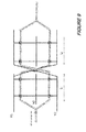
- FIG. 9 shows a schematic illustration of generalized robust Mach-Zehnder modulator according to an aspect of the present disclosure.
- any element expressed as a means for performing a specified function is intended to encompass any way of performing that function including, for example, a) a combination of circuit elements which performs that function or b) software in any form, including, therefore, firmware, microcode or the like, combined with appropriate circuitry for executing that software to perform the function.
- the invention as defined by such claims resides in the fact that the functionalities provided by the various recited means are combined and brought together in the manner which the claims call for. Applicant thus regards any means which can provide those functionalities as equivalent as those shown herein.
- one commonly used optical modulator type employs lateral pn diodes to achieve phase modulation.
- pn diodes may be used in either forward- or reverse-biased.
- SOI Silicon-on-Insulator
- the modulator cross section shown may be processed using four lithography steps and corresponding mask(s).
- two process steps namely, a shallow etch step and a deep etch step define the waveguide geometry.
- Two doping steps namely, the p doping step and the n doping step define the pn junction.
- modulator loss ⁇ , modulation efficiency V ⁇ L ⁇ and to a lesser extent the bandwidth will be dependent upon the position of the pn junction with respect to the optical mode.
- any mask misalignment of the etch steps or doping steps will result in a ship of the pn junction position with respect to the optical mode—resulting in a change in absorption or modulation efficiency.
- FIG. 2 illustrates a mask misalignment for waveguide modulators with opposite oriented pn junction.
- FIG. 2 With reference to that FIG. 2 , there is illustrated a junction shift x shifted to the left (as viewing the figure) for an np junction and shifts to the right for a pn junction.
- This shift results in two types of modulators that—while designed to be exactly the same—but behave differently due to the non-ideal processing, i.e., mask misalignment. Those skilled in the art will appreciate that this is caused by a difference in overlap between the pn junction and the optical waveguide mode for pn junctions with different orientation.
- a Mach-Zehnder Interferometer (MZI) circuit such as that illustratively shown in FIG. 3 , is used to transform a phase modulation into an amplitude modulation.
- MZI circuit should is balanced, meaning that the optical loss in both arms, i.e., phase modulator 1 and phase modulator 2 , should be equal.
- the modulators are biased at a certain bias voltage V 0 , and driven with opposite voltages.
- the modulators are so-called travelling wave modulators, which are designed such that the speed of the microwave in the transmission line steering the modulator and the optical mode in the waveguide are equal.
- an impedance matching termination resistor is placed at the end of the transmission line to avoid reflections.
- travelling wave MZI modulator When using a travelling wave MZI modulator, different kinds of configurations are possible. Choosing a suitable configuration depends on several factors such as material platform, driver chip used to drive the modulator, modulation bandwidth, impedance of the feed transmission lines of the modulator and required voltage swing.
- phase chirp is not a major concern is to only drive one arm of the MZI modulator using pn junctions—for example.
- the MZI is then balanced by introducing dummy pn junctions in the non-modulated arm. By making sure that these dummy pn junctions have the same orientation as the ones in the arm that is modulated, the same optical loss is introduced independent of the mask misalignment.
- an asymmetric power splitter may be used to compensate for the loss in the waveguide arm that is modulated. Additionally, by making the power splitter tunable, it is possible to compensate for mask misalignments.
- the MZI modulator needs to be driven in a push-pull configuration. When so driven, the modulator is then biased at V 0 and driven by opposite voltages. Equalizing the loss is typically achieved by having pn junctions with the same orientation in both arms.
- FIG. 4 This configuration where each modulator is driven by its own transmission line is illustratively depicted in FIG. 4 .
- FIG. 4 there is shown a push-pull MZI modulator with equally oriented pn junctions in both waveguide arms and controlled by two transmission lines.
- the loss in both waveguide arms is the loss ⁇ 1 introduced by the pn junctions times the modulation length Lm.
- One drawback of this configuration shown is that bandwidth is reduced because the diodes are configured in parallel.
- the bandwidth is determined by the loss introduced by the RF lines. This RF loss or microwave attenuation will decrease when the capacitance per unit length can be decreased.
- One example is to drive the push-pull modulator by one differential transmission line and having the pn junctions in series, as shown in FIG. 5 .
- FIG. 5 illustrates a push-pull modulator with opposite oriented pn junctions in series and driven by a differential transmission line. This configuration shown will decrease the capacitance per unit length by a factor of 2.
- circuits according to the present disclosure may advantageously be very general and applied to a broad class of modulator configurations to compensate for mask misalignment in lateral doped waveguide junctions.
- both arms of the MZI modulator in push-pull configuration experience the same length of waveguide with a pn junction having a particular orientation. Consequently, this equalizes the optical loss and modulation efficiency in both MZI arms thereby realizing a balanced MZI modulator in push-pull mode without exhibiting phase chirp.
- FIG. 6 there is shown a mask misaligned compensated MZI push-pull modulator with crossed signal lines, switched pn junctions and switched bias according to an aspect of the present disclosure.
- the pn junction orientation in the arms is effectively switched after one half of the length Lm of the modulator.
- the signal lines of the differential transmission lines have to be switched and the bias V 0 is reversed for the second half of the modulator.
- such a configuration results in both modulator arms experiencing an equal modulation efficiency and an equal optical loss which may be expressed as ( ⁇ 1+ ⁇ 2)Lm/2.
- FIG. 7 Another exemplary configuration according to the present disclosure is illustratively shown in FIG. 7 , which illustratively shows a mask misalignment compensated MZI push-pull modulator with crossed signal lines and crossed optical waveguide according to yet another aspect of the present disclosure.
- the optical waveguides are switched by crossing them as illustrated in this figure.
- the signal lines of the differential transmission lines are switched as well.
- crossing the waveguides may be performed with very low loss and crosstalk.
- the crossing may be perfectly symmetrical so that both waveguides will experience the exact same amount of optical loss and delay.
- Crossing the signal lines of the differential transmission line is more difficult but may be done using an additional metal layer and vias, air bridge or wire bond for example. This crossing is typically not symmetrical and therefore more RF loss and/or Rf delay is introduced into one of the signal lines thereby resulting in an asymmetry.
- One possible solution to this asymmetry is to introduce a dummy transition in one of the signal lines such that the difference in RF loss and delay is compensated.
- FIG. 8 shows compensation of RF crossing asymmetry using an even amount of RF crossings.
- an extra optical delay is introduced to compensate for the RF delays of the RF crossing(s).
- two complementary RF transitions equalize the RF attenuation and RF delay in both signal lines.
- An extra optical delay is introduced at the RF crossings to compensate for the RF delays.
- One possible alternative solution where no signal line crossing is needed is to drive the modulator using at least two staggered feeding differential transmission lines which are delayed as necessary. Such an approach may be quite useful for modulators using distributed drivers integrated onto a same chip. However, if the drivers are not integrated this may increase the number of RF connections and terminations by a two-fold amount.
- FIG. 9 there is shown a more generalized MZI modulator constructed according to an aspect of the present disclosure. As may be observed, any bias voltage is left floating and the crossings need not be restricted to one according to the present disclosure. A principal of the scheme depicted is tha the MZI is inherently balanced, independent of any mask misalignments.
Landscapes
- Physics & Mathematics (AREA)
- Nonlinear Science (AREA)
- General Physics & Mathematics (AREA)
- Optics & Photonics (AREA)
- Optical Modulation, Optical Deflection, Nonlinear Optics, Optical Demodulation, Optical Logic Elements (AREA)
Abstract
Description
Claims (21)
Priority Applications (1)
| Application Number | Priority Date | Filing Date | Title |
|---|---|---|---|
| US14/057,883 US9372381B2 (en) | 2012-10-18 | 2013-10-18 | Robust modulator circuits using lateral doping junctions |
Applications Claiming Priority (2)
| Application Number | Priority Date | Filing Date | Title |
|---|---|---|---|
| US201261715514P | 2012-10-18 | 2012-10-18 | |
| US14/057,883 US9372381B2 (en) | 2012-10-18 | 2013-10-18 | Robust modulator circuits using lateral doping junctions |
Publications (2)
| Publication Number | Publication Date |
|---|---|
| US20140112611A1 US20140112611A1 (en) | 2014-04-24 |
| US9372381B2 true US9372381B2 (en) | 2016-06-21 |
Family
ID=50485409
Family Applications (1)
| Application Number | Title | Priority Date | Filing Date |
|---|---|---|---|
| US14/057,883 Active US9372381B2 (en) | 2012-10-18 | 2013-10-18 | Robust modulator circuits using lateral doping junctions |
Country Status (1)
| Country | Link |
|---|---|
| US (1) | US9372381B2 (en) |
Cited By (5)
| Publication number | Priority date | Publication date | Assignee | Title |
|---|---|---|---|---|
| US20170123155A1 (en) * | 2014-07-16 | 2017-05-04 | Huawei Technologies Co., Ltd. | Cross waveguide |
| US20220373828A1 (en) * | 2021-05-18 | 2022-11-24 | Fujitsu Optical Components Limited | Optical device and optical communication apparatus |
| US20220390775A1 (en) * | 2021-06-03 | 2022-12-08 | Fujitsu Optical Components Limited | Optical device and optical communication apparatus |
| US11552710B2 (en) | 2020-08-17 | 2023-01-10 | Acacia Communications, Inc. | Resistivity engineered substrate for RF common-mode suppression |
| US11556020B1 (en) | 2020-07-29 | 2023-01-17 | Acacia Communications, Inc. | Integrated wavelength selector |
Families Citing this family (21)
| Publication number | Priority date | Publication date | Assignee | Title |
|---|---|---|---|---|
| US8731410B2 (en) | 2007-10-02 | 2014-05-20 | Luxtera, Inc. | Method and system for split voltage domain receiver circuits |
| US9817249B2 (en) * | 2012-06-26 | 2017-11-14 | Acacia Communications, Inc. | Alternating traveling-wave Mach-Zehnder modulator |
| US10078232B1 (en) | 2014-07-11 | 2018-09-18 | Acacia Communications, Inc. | Advanced optical modulation generation by combining orthogonal polarized optical signals |
| US9632390B1 (en) * | 2015-03-06 | 2017-04-25 | Inphi Corporation | Balanced Mach-Zehnder modulator |
| EP3333619B1 (en) * | 2015-08-04 | 2020-04-15 | Nippon Telegraph And Telephone Corporation | Optical modulator |
| JP6603571B2 (en) * | 2015-12-17 | 2019-11-06 | 日本電信電話株式会社 | Light modulator |
| US10133142B2 (en) * | 2016-03-29 | 2018-11-20 | Acacia Communications, Inc. | Silicon modulators and related apparatus and methods |
| JP6581541B2 (en) * | 2016-05-27 | 2019-09-25 | 日本電信電話株式会社 | Light modulator |
| US10120210B2 (en) | 2016-06-03 | 2018-11-06 | International Business Machines Corporation | Feed-forward optical equalization using an electro-optic modulator with a multi-segment electrode and distributed drivers |
| US10084619B2 (en) | 2016-06-03 | 2018-09-25 | International Business Machines Corporation | Nested feed-forward optical equalization using an electro-optic modulator with a multi-segment electrode |
| US10088733B2 (en) | 2016-08-08 | 2018-10-02 | Acacia Communications, Inc. | Segmented traveling wave optical modulators and related methods |
| JP6781618B2 (en) * | 2016-12-09 | 2020-11-04 | 日本電信電話株式会社 | Light modulator |
| US10488683B1 (en) * | 2017-03-06 | 2019-11-26 | Acacia Communications, Inc. | Traveling wave modulator |
| US11460724B2 (en) | 2017-04-28 | 2022-10-04 | Ciena Corporation | Optical modulator robust to fabrication errors through an RF electrical crossing |
| US10330961B2 (en) * | 2017-04-28 | 2019-06-25 | Ciena Corporation | Optical modulator robust to fabrication errors |
| JP6734813B2 (en) * | 2017-05-30 | 2020-08-05 | 日本電信電話株式会社 | Optical transmitter |
| JP6950400B2 (en) * | 2017-09-22 | 2021-10-13 | 住友電気工業株式会社 | Mach Zenda Modulator |
| US11378826B2 (en) * | 2019-09-17 | 2022-07-05 | Lumentum Operations Llc | Electrical-optical modulator |
| CN113014323B (en) | 2019-12-20 | 2024-02-09 | 光联通讯技术有限公司美国分部 | Optical transmission device and optical communication system |
| WO2022026575A1 (en) * | 2020-07-31 | 2022-02-03 | Ciena Corporation | Optical modulator robust to fabrication errors through an rf electrical crossing |
| JP2022073196A (en) * | 2020-10-30 | 2022-05-17 | 住友大阪セメント株式会社 | Optical waveguide element, optical waveguide device, and optical transmission apparatus |
Citations (2)
| Publication number | Priority date | Publication date | Assignee | Title |
|---|---|---|---|---|
| US5745630A (en) * | 1996-02-22 | 1998-04-28 | Sandia Corporation | Cutoff-mesa isolated rib optical waveguide for III-V heterostructure photonic integrated circuits |
| US20140341497A1 (en) * | 2013-05-14 | 2014-11-20 | Yang Liu | Ultra-responsive phase shifters for depletion mode silicon modulators |
-
2013
- 2013-10-18 US US14/057,883 patent/US9372381B2/en active Active
Patent Citations (2)
| Publication number | Priority date | Publication date | Assignee | Title |
|---|---|---|---|---|
| US5745630A (en) * | 1996-02-22 | 1998-04-28 | Sandia Corporation | Cutoff-mesa isolated rib optical waveguide for III-V heterostructure photonic integrated circuits |
| US20140341497A1 (en) * | 2013-05-14 | 2014-11-20 | Yang Liu | Ultra-responsive phase shifters for depletion mode silicon modulators |
Non-Patent Citations (5)
| Title |
|---|
| Bogaerts et al., Silicon nanophotonic waveguides and their applications. Proc SPIE. Nov. 2008;7134:71341O.1-13. doi: 10.1117/12.803440. |
| Chen et al., Chirp and Dispersion Tolerance of a Single-Drive Push-Pull Silicon Modulator at 28 Gb/s. IEEE Photon Tech Lett. Mar. 15, 2012;24(11):936-8. doi: 10.1109/LPT.2012.2191149. |
| Kikuchi et al., 80-Gbit/s InP DQPSK modulator with an n-p-i-n structure. 2007 33rd European Conference and Exhibition of Optical Communication (ECOC), Berlin, Germany. Sep. 16-20, 2007;2(1):8-9. doi: 10.1049/ic:20070367. 2 pages. |
| Park et al., High-modulation efficiency silicon Mach-Zehnder optical modulator based on carrier depletion in a PN Diode. Opt Express. Aug. 31, 2009;17(18):15520-4. |
| Thompson et al., High contrast 40 Gbit/s optical modulation in silicon. Opt Express. Jun. 6, 2011;19(12):11507-16. doi: 10.1364/OE.19.011507. |
Cited By (6)
| Publication number | Priority date | Publication date | Assignee | Title |
|---|---|---|---|---|
| US20170123155A1 (en) * | 2014-07-16 | 2017-05-04 | Huawei Technologies Co., Ltd. | Cross waveguide |
| US9766399B2 (en) * | 2014-07-16 | 2017-09-19 | Huawei Technologies Co., Ltd. | Cross waveguide |
| US11556020B1 (en) | 2020-07-29 | 2023-01-17 | Acacia Communications, Inc. | Integrated wavelength selector |
| US11552710B2 (en) | 2020-08-17 | 2023-01-10 | Acacia Communications, Inc. | Resistivity engineered substrate for RF common-mode suppression |
| US20220373828A1 (en) * | 2021-05-18 | 2022-11-24 | Fujitsu Optical Components Limited | Optical device and optical communication apparatus |
| US20220390775A1 (en) * | 2021-06-03 | 2022-12-08 | Fujitsu Optical Components Limited | Optical device and optical communication apparatus |
Also Published As
| Publication number | Publication date |
|---|---|
| US20140112611A1 (en) | 2014-04-24 |
Similar Documents
| Publication | Publication Date | Title |
|---|---|---|
| US9372381B2 (en) | Robust modulator circuits using lateral doping junctions | |
| US11599005B2 (en) | Optical waveguide modulator | |
| CN102782567B (en) | Having can the photomodulator of control linear frequency modulation on pulse | |
| US10146099B2 (en) | Optical modulator | |
| US7826689B2 (en) | Optical device which outputs independently modulated light beams in respective TE and TM polarization modes | |
| US6721085B2 (en) | Optical modulator and design method therefor | |
| KR20120075461A (en) | Advanced modulation formats for silicon-based optical modulators | |
| CN112596277A (en) | Electro-optic modulator | |
| US9128310B2 (en) | Advanced modulation format using two-state modulators | |
| EP3403138B1 (en) | An optical apparatus | |
| US11112623B1 (en) | Distributed CMOS driver with enhanced drive voltage for silicon optical push-pull Mach-Zehnder modulators | |
| US9846347B2 (en) | Balanced Mach-Zehnder modulator | |
| US11768392B2 (en) | Optical modulator robust to fabrication errors through an RF electrical crossing | |
| US8634678B2 (en) | Phase shifter and electro-optic modulation device including the same | |
| US20150063742A1 (en) | Method for modulating a carrier light wave | |
| JP2010250125A (en) | Optical modulator | |
| US10330961B2 (en) | Optical modulator robust to fabrication errors | |
| JP2009204884A (en) | Light modulating device | |
| JP2015148711A (en) | Semiconductor mach-zehnder light modulator | |
| JP2017211607A (en) | Optical modulator | |
| US11467467B2 (en) | Optical modulator | |
| WO2020202596A1 (en) | Optical modulator | |
| US20230084020A1 (en) | Providing a Drive Signal for Optical Modulator Portions | |
| JP2015212769A (en) | Semiconductor Mach-Zehnder optical modulator | |
| JP7263966B2 (en) | optical device |
Legal Events
| Date | Code | Title | Description |
|---|---|---|---|
| AS | Assignment |
Owner name: ACACIA COMMUNICATIONS, INC., MASSACHUSETTS Free format text: ASSIGNMENT OF ASSIGNORS INTEREST;ASSIGNOR:VERMEULEN, DIEDRIK;REEL/FRAME:036098/0401 Effective date: 20150701 |
|
| AS | Assignment |
Owner name: ACACIA COMMUNICATIONS, INC., MASSACHUSETTS Free format text: ASSIGNMENT OF ASSIGNORS INTEREST;ASSIGNORS:CHEN, LONG;DOERR, CHRISTOPHER;SIGNING DATES FROM 20150916 TO 20150918;REEL/FRAME:037863/0001 |
|
| STCF | Information on status: patent grant |
Free format text: PATENTED CASE |
|
| CC | Certificate of correction | ||
| MAFP | Maintenance fee payment |
Free format text: PAYMENT OF MAINTENANCE FEE, 4TH YR, SMALL ENTITY (ORIGINAL EVENT CODE: M2551); ENTITY STATUS OF PATENT OWNER: SMALL ENTITY Year of fee payment: 4 |
|
| FEPP | Fee payment procedure |
Free format text: ENTITY STATUS SET TO UNDISCOUNTED (ORIGINAL EVENT CODE: BIG.); ENTITY STATUS OF PATENT OWNER: LARGE ENTITY |
|
| MAFP | Maintenance fee payment |
Free format text: PAYMENT OF MAINTENANCE FEE, 8TH YEAR, LARGE ENTITY (ORIGINAL EVENT CODE: M1552); ENTITY STATUS OF PATENT OWNER: LARGE ENTITY Year of fee payment: 8 |
|
| AS | Assignment |
Owner name: ACACIA TECHNOLOGY, INC., CALIFORNIA Free format text: ASSIGNMENT OF ASSIGNORS INTEREST;ASSIGNOR:ACACIA COMMUNICATIONS, INC.;REEL/FRAME:066832/0659 Effective date: 20230712 |