US9252683B2 - Tracking converters with input output linearization control - Google Patents
Tracking converters with input output linearization control Download PDFInfo
- Publication number
- US9252683B2 US9252683B2 US13/938,333 US201313938333A US9252683B2 US 9252683 B2 US9252683 B2 US 9252683B2 US 201313938333 A US201313938333 A US 201313938333A US 9252683 B2 US9252683 B2 US 9252683B2
- Authority
- US
- United States
- Prior art keywords
- voltage
- converter circuit
- output voltage
- time
- inductor
- Prior art date
- Legal status (The legal status is an assumption and is not a legal conclusion. Google has not performed a legal analysis and makes no representation as to the accuracy of the status listed.)
- Expired - Fee Related, expires
Links
- 238000000034 method Methods 0.000 claims description 41
- 239000003990 capacitor Substances 0.000 claims description 31
- 238000001228 spectrum Methods 0.000 claims description 12
- 230000000694 effects Effects 0.000 abstract description 5
- 230000006870 function Effects 0.000 description 33
- 238000005070 sampling Methods 0.000 description 17
- 238000010586 diagram Methods 0.000 description 8
- 239000011159 matrix material Substances 0.000 description 7
- 238000006243 chemical reaction Methods 0.000 description 6
- 230000001052 transient effect Effects 0.000 description 5
- 230000004044 response Effects 0.000 description 4
- 238000012935 Averaging Methods 0.000 description 3
- 230000008571 general function Effects 0.000 description 3
- 230000008901 benefit Effects 0.000 description 2
- 230000008569 process Effects 0.000 description 2
- 230000003068 static effect Effects 0.000 description 2
- 230000009022 nonlinear effect Effects 0.000 description 1
- 229910052710 silicon Inorganic materials 0.000 description 1
- 239000010703 silicon Substances 0.000 description 1
- 230000000087 stabilizing effect Effects 0.000 description 1
- 230000009466 transformation Effects 0.000 description 1
Images
Classifications
-
- H—ELECTRICITY
- H02—GENERATION; CONVERSION OR DISTRIBUTION OF ELECTRIC POWER
- H02M—APPARATUS FOR CONVERSION BETWEEN AC AND AC, BETWEEN AC AND DC, OR BETWEEN DC AND DC, AND FOR USE WITH MAINS OR SIMILAR POWER SUPPLY SYSTEMS; CONVERSION OF DC OR AC INPUT POWER INTO SURGE OUTPUT POWER; CONTROL OR REGULATION THEREOF
- H02M7/00—Conversion of ac power input into dc power output; Conversion of dc power input into ac power output
- H02M7/42—Conversion of dc power input into ac power output without possibility of reversal
- H02M7/44—Conversion of dc power input into ac power output without possibility of reversal by static converters
- H02M7/48—Conversion of dc power input into ac power output without possibility of reversal by static converters using discharge tubes with control electrode or semiconductor devices with control electrode
- H02M7/53—Conversion of dc power input into ac power output without possibility of reversal by static converters using discharge tubes with control electrode or semiconductor devices with control electrode using devices of a triode or transistor type requiring continuous application of a control signal
- H02M7/537—Conversion of dc power input into ac power output without possibility of reversal by static converters using discharge tubes with control electrode or semiconductor devices with control electrode using devices of a triode or transistor type requiring continuous application of a control signal using semiconductor devices only, e.g. single switched pulse inverters
- H02M7/539—Conversion of dc power input into ac power output without possibility of reversal by static converters using discharge tubes with control electrode or semiconductor devices with control electrode using devices of a triode or transistor type requiring continuous application of a control signal using semiconductor devices only, e.g. single switched pulse inverters with automatic control of output wave form or frequency
- H02M7/5395—Conversion of dc power input into ac power output without possibility of reversal by static converters using discharge tubes with control electrode or semiconductor devices with control electrode using devices of a triode or transistor type requiring continuous application of a control signal using semiconductor devices only, e.g. single switched pulse inverters with automatic control of output wave form or frequency by pulse-width modulation
-
- H—ELECTRICITY
- H02—GENERATION; CONVERSION OR DISTRIBUTION OF ELECTRIC POWER
- H02M—APPARATUS FOR CONVERSION BETWEEN AC AND AC, BETWEEN AC AND DC, OR BETWEEN DC AND DC, AND FOR USE WITH MAINS OR SIMILAR POWER SUPPLY SYSTEMS; CONVERSION OF DC OR AC INPUT POWER INTO SURGE OUTPUT POWER; CONTROL OR REGULATION THEREOF
- H02M3/00—Conversion of dc power input into dc power output
- H02M3/02—Conversion of dc power input into dc power output without intermediate conversion into ac
- H02M3/04—Conversion of dc power input into dc power output without intermediate conversion into ac by static converters
- H02M3/10—Conversion of dc power input into dc power output without intermediate conversion into ac by static converters using discharge tubes with control electrode or semiconductor devices with control electrode
- H02M3/145—Conversion of dc power input into dc power output without intermediate conversion into ac by static converters using discharge tubes with control electrode or semiconductor devices with control electrode using devices of a triode or transistor type requiring continuous application of a control signal
- H02M3/155—Conversion of dc power input into dc power output without intermediate conversion into ac by static converters using discharge tubes with control electrode or semiconductor devices with control electrode using devices of a triode or transistor type requiring continuous application of a control signal using semiconductor devices only
- H02M3/156—Conversion of dc power input into dc power output without intermediate conversion into ac by static converters using discharge tubes with control electrode or semiconductor devices with control electrode using devices of a triode or transistor type requiring continuous application of a control signal using semiconductor devices only with automatic control of output voltage or current, e.g. switching regulators
- H02M3/158—Conversion of dc power input into dc power output without intermediate conversion into ac by static converters using discharge tubes with control electrode or semiconductor devices with control electrode using devices of a triode or transistor type requiring continuous application of a control signal using semiconductor devices only with automatic control of output voltage or current, e.g. switching regulators including plural semiconductor devices as final control devices for a single load
- H02M3/1582—Buck-boost converters
-
- H—ELECTRICITY
- H02—GENERATION; CONVERSION OR DISTRIBUTION OF ELECTRIC POWER
- H02M—APPARATUS FOR CONVERSION BETWEEN AC AND AC, BETWEEN AC AND DC, OR BETWEEN DC AND DC, AND FOR USE WITH MAINS OR SIMILAR POWER SUPPLY SYSTEMS; CONVERSION OF DC OR AC INPUT POWER INTO SURGE OUTPUT POWER; CONTROL OR REGULATION THEREOF
- H02M1/00—Details of apparatus for conversion
- H02M1/0003—Details of control, feedback or regulation circuits
- H02M1/0012—Control circuits using digital or numerical techniques
-
- H—ELECTRICITY
- H02—GENERATION; CONVERSION OR DISTRIBUTION OF ELECTRIC POWER
- H02M—APPARATUS FOR CONVERSION BETWEEN AC AND AC, BETWEEN AC AND DC, OR BETWEEN DC AND DC, AND FOR USE WITH MAINS OR SIMILAR POWER SUPPLY SYSTEMS; CONVERSION OF DC OR AC INPUT POWER INTO SURGE OUTPUT POWER; CONTROL OR REGULATION THEREOF
- H02M1/00—Details of apparatus for conversion
- H02M1/0083—Converters characterised by their input or output configuration
- H02M1/009—Converters characterised by their input or output configuration having two or more independently controlled outputs
-
- H02M2001/0012—
-
- H02M2001/009—
-
- H—ELECTRICITY
- H02—GENERATION; CONVERSION OR DISTRIBUTION OF ELECTRIC POWER
- H02M—APPARATUS FOR CONVERSION BETWEEN AC AND AC, BETWEEN AC AND DC, OR BETWEEN DC AND DC, AND FOR USE WITH MAINS OR SIMILAR POWER SUPPLY SYSTEMS; CONVERSION OF DC OR AC INPUT POWER INTO SURGE OUTPUT POWER; CONTROL OR REGULATION THEREOF
- H02M3/00—Conversion of dc power input into dc power output
- H02M3/02—Conversion of dc power input into dc power output without intermediate conversion into ac
- H02M3/04—Conversion of dc power input into dc power output without intermediate conversion into ac by static converters
- H02M3/10—Conversion of dc power input into dc power output without intermediate conversion into ac by static converters using discharge tubes with control electrode or semiconductor devices with control electrode
- H02M3/145—Conversion of dc power input into dc power output without intermediate conversion into ac by static converters using discharge tubes with control electrode or semiconductor devices with control electrode using devices of a triode or transistor type requiring continuous application of a control signal
- H02M3/155—Conversion of dc power input into dc power output without intermediate conversion into ac by static converters using discharge tubes with control electrode or semiconductor devices with control electrode using devices of a triode or transistor type requiring continuous application of a control signal using semiconductor devices only
- H02M3/156—Conversion of dc power input into dc power output without intermediate conversion into ac by static converters using discharge tubes with control electrode or semiconductor devices with control electrode using devices of a triode or transistor type requiring continuous application of a control signal using semiconductor devices only with automatic control of output voltage or current, e.g. switching regulators
- H02M3/158—Conversion of dc power input into dc power output without intermediate conversion into ac by static converters using discharge tubes with control electrode or semiconductor devices with control electrode using devices of a triode or transistor type requiring continuous application of a control signal using semiconductor devices only with automatic control of output voltage or current, e.g. switching regulators including plural semiconductor devices as final control devices for a single load
-
- H—ELECTRICITY
- H03—ELECTRONIC CIRCUITRY
- H03K—PULSE TECHNIQUE
- H03K7/00—Modulating pulses with a continuously-variable modulating signal
- H03K7/08—Duration or width modulation ; Duty cycle modulation
Definitions
- the present invention relates generally to providing modulation signals to electrical circuits and, more particularly, to tracking inverters and tracking converters based on input-output linearization control.
- Power converters are used to convert one form of energy to another (e.g., AC to AC, AC to DC, DC to AC, and DC to DC) thereby making it usable to the end equipment, such as computers, automobiles, electronics, telecommunications, space systems and satellites, and motors. Every application of power electronics involves some aspect of control.
- Converters are typically identified by their capability and/or configurations, such as, buck converters, boost converters, buck-boost converters, boost-buck converters ( ⁇ uk), etc. These converters can belong to a family of converters known as “switching regulators” (DC-DC conversion), “switching converters”, or “switching inverters” (DC-AC conversion) depending upon their configuration.
- Switching converters are generally efficient because the conversion elements switch from one state to another, rather than needlessly dissipating power during the conversion process.
- a converter circuit including a set of switches and at least two configurations of the converter, according to the states of the set of switches.
- Each configuration can be modeled as linear system.
- the duty ratio (d) is the ratio indicating the time in while one switch is in the “on” position and another switch is in the “off” position: this d is considered to be the control input.
- Control input d is usually driven by pulse-width-modulation (“PWM”) techniques.
- PWM pulse-width-modulation
- TEM trailing-edge modulation
- CCM continuous conduction mode
- LEM the on-time pulse begins in accordance with a control law and terminates on the clock.
- the difference between LEM and TEM is that in TEM the pulse-width is determined by the instantaneous control voltage v c prior to switch turn-off, whereas in LEM the pulse-width is determined by v c prior to switch turn-on.
- PWM pulse-width modulation
- ESR equivalent series resistance
- a voltage inverter comprising a voltage converter circuit and a controller.
- the voltage inverter produces a time-varying output voltage from an input voltage, where the input voltage can be a DC voltage, an AC input voltage at a given input frequency or a time-varying voltage signal having a given input frequency spectrum.
- the controller provides a control signal at a duty ratio determined dynamically by a set of signals.
- the set of signals include the time-varying output voltage, a predetermined output voltage, a gain factor and an inductor current in the voltage converter circuit.
- the predetermined output voltage can have an output AC waveform or an arbitrary time-varying waveform.
- the output AC waveform can have an output frequency different than the input frequency.
- the arbitrary time-varying waveform can have an output frequency spectrum different than the input frequency spectrum.
- the voltage inverter operates to match the time-varying output voltage to the predetermined output voltage.
- Input-output linearization is used to design various inverters under conditions where left half plane zero effects are present.
- a time-varying duty cycle for the control signal is derived for a voltage inverter where the voltage converter circuit is a buck converter circuit.
- a time-varying duty cycle for the control signal is derived for a voltage inverter where the voltage converter circuit is a boost converter circuit and leading edge modulation is used.
- a time-varying duty cycle for the control signal is derived for a voltage inverter where the voltage converter circuit is a buck-boost converter circuit and leading edge modulation is used.
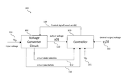
- FIG. 1 is a block diagram of a preferred embodiment of a tracking inverter including a voltage converter circuit and a controller.
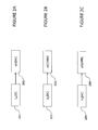
- FIG. 2A is a block diagram of a tracking inverter producing an AC output from a DC input.
- FIG. 2B is a block diagram of a tracking inverter producing an arbitrary output waveform from a DC input.
- FIG. 2C is a block diagram of a tracking inverter producing an arbitrary output waveform from an AC input.
- FIG. 3 is a circuit diagram of a buck converter of a preferred embodiment.
- FIG. 4 is a circuit diagram of a boost converter of a preferred embodiment.
- FIG. 5 is a circuit diagram of a buck-boost converter of a preferred embodiment.
- FIG. 6 is a flow chart of a method of operation for a preferred embodiment of a voltage inverter.
- FIG. 7 is a block diagram of a multiple output tracking inverter.
- the present disclosure provides a method and apparatus for controlling a voltage converter circuit to realize a power inverter.
- a power inverter in power electronics usually refers to a power converter device that delivers an ac output voltage in response to a dc input voltage. More generally, the present disclosure delivers an arbitrary time-varying output waveform for one of either a dc voltage input or an ac voltage input. In particular, the present disclosure uses input-output linearization to compute a duty ratio for control feedback of a voltage converter.
- Embodiments for a buck converter, a boost converter and a buck-boost converter are disclosed, where the boost and buck-boost converters use off-time sampling with either leading edge modulation or trailing edge modulation.
- the resulting control system can also be applied to other converter types.
- the parameters in the control system are programmable, and hence the algorithm can be easily implemented on a DSP or in silicon, such as an ASIC.
- buck, boost, and buck-boost converter circuits are characterized by state equations for state variables x 1 (inductor current), x 2 (capacitor voltage) and y (output voltage).
- a control signal is applied to a primary switch (S 1 ) characterized by its instantaneous duty ratio d.
- the steady-state output voltage of a boost voltage converter is 1/(1 ⁇ D) times the input voltage where D is the steady-state value of the instantaneous duty ratio d.
- the steady-state output voltage of a buck-boost converter is D/(1 ⁇ D) times the input voltage and the steady-state output voltage of a buck converter is D times the input voltage.
- y(t) and the resultant duty ratio d(t) also varies with time.
- FIG. 1 shows a preferred embodiment of a tracking inverter 100 suitable for controlling a voltage converter circuit to produce a time varying output voltage.
- Tracking inverter 100 is amenable to input-output linearization methods that do not constrain stability to one operating point, but rather to a set of operating points spanning the expected range of operation during startup and transient modes of operation.
- a voltage converter circuit 102 is connected to an input voltage 101 (u 0 ) and produces output voltage 110 , y(t), in response to a control signal 109 characterized by the duty ratio d(t).
- output voltage 110 is a time varying waveform intended to match a desired output voltage 115 , y 0 (t), also time varying.
- Controller 120 produces control signal 109 from sensing output voltage 110 , input voltage 101 , desired output voltage 115 , a set of static circuit parameters 113 including, for example, the load resistance R, the capacitance C and the inductance L, and a set of state variables 112 including, for example, inductor current x 1 and capacitor voltage x 2 .
- Control signal 109 determines the states of a set of switches internal to voltage converter circuit 102 .
- Controller 120 is preferably implemented in one or more digital devices, implemented with programmable software instructions stored in memory and executed by a processor to carry out the converter control functions including output adjustment.
- a processor to carry out the converter control functions including output adjustment.
- an analog implementation is used instead of a digital implementation.
- the controller methods as described below are then implemented as hardware functions, including analog adders and multipliers.
- Controller 120 can implement any desired control method.
- a pulse width modulated (PWM) controller is suitably constructed.
- the PWM controller produces a time varying control signal which drives the primary switch (S 1 ) of a voltage converter with the duty ratio d.
- Examples of voltage converter circuit 102 include a buck converter, a boost converter and a buck-boost converter.
- Voltage converters operating in the continuous conduction mode with trailing edge modulation (TEM) and switch on-time sampling give rise to unstable zero dynamics for boost and buck-boost converters where the linear segment of the system about an operating point has a right half plane zero.
- leading-edge modulation (LEM) with switch-off time sampling is implemented by controller 120 that changes the zero dynamics, so that the linear part of the system has only left half plane zeros.
- trailing-edge modulation (TEM) with switch-off time sampling is implemented.
- input-output feedback linearization can be employed wherein a linearizing transformation is performed and used to define control signal inputs to a converter.
- the control signal duty ratios and resulting zero dynamics for boost and buck-boost converters are the same for both LEM and TEM with switch-off time sampling.
- a buck converter is a linear system which has a left half plane zero in its transfer function, therefore, input-output linearization can always be employed, regardless of the modulation method used.
- An inverter in power electronics usually refers to a power converter device delivering a sinusoidal AC output voltage in response to a DC input voltage.
- voltage converters that have general bounded time functions, not just sinusoidal waveforms, as the desired output voltages. These converters will be known as tracking inverters.
- the tracking inverter supports a steady state tracking inversion, which is the process of establishing a control signal d(t) so that the output voltage y(t) converges to the desired output voltage y 0 (t) as time, t, goes to infinity.
- Tracking inverters, based on buck, boost and buck-boost converters are analyzed using their respective Cuk-Middlebrook two dimensional state space averaged models.
- a DC-AC tracking inverter converts a DC input voltage 201 to an AC output voltage 202 varying with time in a sinusoidal function.
- a tracking inverter function converts a DC input voltage 203 to an arbitrary time-varying output voltage 204 having an arbitrary waveform and arbitrary frequency spectrum.
- a tracking inverter converts an AC input voltage 205 to an arbitrary time-varying output voltage 206 .
- the input voltage u 0 may have an input waveform characterized by an input frequency while the output voltage y(t) may have an output waveform characterized by an output frequency.
- the output waveform can be different than the input waveform and the output frequency can be different than the input frequency.
- the output frequency spectrum can be different that the input frequency spectrum for more complex waveforms.
- Eq. 1 y y for state variables x 1 , output voltage y and control signal duty ratio d. It is assumed that the transfer function of Eq. 1 has no pole zero cancellations. The zero z of the transfer function is found by setting the determinant of the matrix
- x . 1 ( a 22 - a 12 ⁇ b 2 b 1 ) ⁇ x 1 + ( a 21 - a 11 ⁇ b 2 b 1 ) ⁇ y 0 + b 2 b 1 ⁇ y . 0 Eq . ⁇ 5
- Proportional output feedback is added and the term a 11 y 0 is replaced by a 11 y in Eq. 4 to form the feedback control signal with time varying duty ratio d(t) defined by
- Eqs. 5-8 show that all solutions (y; x 1 ) tend exponentially to (y 0 ; x 10 ) as time t goes to infinity.
- y(t) converges to y 0 (t) as time t goes to infinity which means that steady state tracking inversion is achieved.
- a time varying desired output voltage y 0 (t) is easily handled by the controller by utilizing the desired output voltage and its derivative, y 0 (t) and ⁇ dot over (y) ⁇ 0 (t) as shown in Eq. 7, computing d Wand applying the feedback control signal with d(t) to the voltage converter circuit.
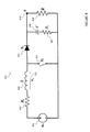
- FIG. 3 illustrates a preferred embodiment buck converter circuit 300 having a single output voltage 310 (y).
- the buck converter comprises a switch 304 (S 1 ) connected in series with a series resistor 302 (R S ) connected to inductor 303 (L) which is further connected to load resistance 308 (R). Switch 304 and load resistance 308 further connect to DC voltage input 301 (u 0 ) to complete a series circuit.
- a switch 305 (S 2 ) is connected between switch 304 and DC voltage input 301 .
- a capacitive circuit is connected in parallel with load resistance 308 and comprises a capacitor 306 (C) connected to a DC series resistance 307 (R C ) associated with capacitor 306 .
- the output voltage 310 is taken across load resistance 308 , is non-negative and is less than DC voltage input 301 .
- the inductor current 312 (x 1 ) is measured as the current through inductor 303 and series resistor 302 .
- buck converter circuit 300 is substituted for voltage converter circuit 102 , and controller 120 .
- the DC voltage input u 0 is a constant and the desired output voltage y 0 (t) is a cosine function. More generally, the desired output voltage y 0 (t) is not just a sinusoidal function, but together with its time derivative, are general functions that are bounded on [0, ⁇ ).
- a switch matrix is employed by the controller to handle the positive, zero, and negative values of u 0 , y 0 and y as required to set the duty ratio.
- the matrix b assumes the values:
- Eq . ⁇ 11 which is continuously computed, for the desired voltage y 0 (t) and the output voltage y, and applied by the controller of FIG. 1 to the buck converter circuit of FIG. 3 .
- the controller implements Eq. 11, y(t) converges to y 0 (t), d(t) converges to a steady-state function D 0 (t) as t goes to infinity and steady-state tracking is achieved for the buck inverter.
- a time varying desired output voltage y 0 (t) is easily handled by the controller by utilizing the desired output voltage and its derivative, y 0 (t) and y 0 (t) as shown in Eq. 11, computing d(t) and applying the feedback control signal with d(t) to the voltage converter circuit.
- u 0 is a time varying function bounded on [0, ⁇ ) and the equations 9, 10 and 11 are adjusted accordingly to derive the duty ratio d(t) and produce the desired output voltage y ⁇ y 0 (t).
- FIG. 4 illustrates a preferred embodiment boost converter circuit 400 having a single output voltage 410 (y).
- the boost converter comprises a series resistor 402 (R s ) connected in series with an inductor 403 (L), a switch 404 (S 1 ) and a DC voltage input 401 (u 0 ).
- a capacitive circuit comprises a switch 405 (S 2 ), connected in series to inductor 403 , further connected in series to a capacitor 406 (C) and DC series resistance 407 (R C ) associated with capacitor 406 .
- Load resistance 408 (R) is connected in parallel with capacitor 406 and DC series resistance 407 .
- Output voltage 410 is taken across load resistance 408 .
- the inductor current 412 (x 1 ) is measured as the current through inductor 403 and series resistor 402 .
- boost converter circuit 400 is substituted for voltage converter circuit 102 , and controller 120 uses LEM with switch off time sampling of the state variables.
- the DC voltage input u 0 is a constant and the desired output voltage y 0 (t) is a cosine function. More generally, the desired output voltage y 0 (t) is not just a sinusoidal function, but together with its time derivative, are general functions that are bounded on [0, ⁇ ).
- a switch matrix is employed by the controller to handle the positive, zero, and negative values of u 0 , y 0 and y as required to set the duty ratio.
- d ⁇ ( t ) ( R + R C ) ⁇ LC ⁇ [ y . 0 ⁇ ( t ) - k ⁇ ( y - y 0 ⁇ ( t ) ) ] + ( RR C ⁇ C + L ) ⁇ y - ( L - R S ⁇ R C ⁇ C ) ⁇ Rx 1 - RR C ⁇ Cu 0 R ⁇ ( R C ⁇ Cy - LR ( R + R C ) ⁇ x 1 ) Eq . ⁇ 15
- integral and derivative gain can also be used to derive d(t).
- y(t) converges to y 0 (t)
- d(t) converges to a steady-state function D 0 (t) as t goes to infinity and steady-state tracking is achieved for the boost inverter.
- a time varying desired output voltage y 0 (t) is easily handled by the controller by utilizing the desired output voltage and its derivative, y 0 (t) and ⁇ dot over (y) ⁇ 0 (t) as shown in Eq. 15, computing d(t) and applying the feedback control signal with d(t) to the voltage converter circuit.
- u 0 is a time varying function bounded on [0, ⁇ ) and the equations 12-15 are adjusted accordingly to derive the duty ratio d(t) and produce the desired output voltage y 0 (t).
- controller 120 uses TEM with switch-off time sampling of the state variables.
- the resulting formula for duty ratio d in Eq. 15 is the same as derived for the preferred embodiment of the boost converter.
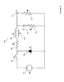
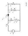
- FIG. 5 illustrates a preferred embodiment buck-boost converter circuit 500 having a single output voltage 510 (y).
- the buck-boost converter comprises a switch 504 (S 1 ) connected in series with series resistor 502 (R s ) which is further connected to an inductor 503 (L). Inductor 503 and switch 504 are connected to DC voltage input 501 (u 0 ) to complete a series circuit.
- a capacitive circuit comprises a switch 505 (S 2 ) connected between switch 504 and a capacitor 506 (C), and further connected in series with DC series resistance 507 (R C ) associated with capacitor 506 .
- Load resistance 508 (R) is connected in parallel with the capacitor 506 and DC series resistance 507 .
- Output voltage 510 is taken across load resistance 508 .
- the inductor current 512 (x 1 ) is measured as the current through inductor 503 and series resistor 502 .
- buck-boost converter circuit 500 is substituted for voltage converter circuit 102 , and controller 120 uses LEM with switch off time sampling of the state variables.
- the DC voltage input u 0 is a constant and the desired output voltage y 0 (t) is a cosine function. More generally, the desired output voltage y 0 (t) is not just a sinusoidal function, but together with its time derivative, are general functions that are bounded on [0, ⁇ ).
- a switch matrix is employed by the controller to handle the positive, zero, and negative values of u 0 , y 0 and y as required to set the duty ratio.
- d ⁇ ( t ) ( R + R C ) ⁇ LC ⁇ [ y . 0 ⁇ ( t ) - k ⁇ ( y - y 0 ⁇ ( t ) ) ] + ( RR C ⁇ C + L ) ⁇ y - ( L - R S ⁇ R C ⁇ ⁇ C ) ⁇ Rx 1 R ⁇ ( R C ⁇ Cy + LR ( R + R C ) ⁇ x 1 - R C ⁇ Cu 0 ) Eq . ⁇ 19
- integral and derivative gain can also be utilized to derive d(t).
- u 0 is a time varying function bounded on [0, ⁇ ) and the equations 16-19 are adjusted accordingly to derive the duty ratio d(t) and produce the desired output voltage y 0 (t).
- controller 120 uses TEM with switch-off time sampling of the state variables.
- the resulting formula for duty ratio d in Eq. 19 is the same as derived for the preferred embodiment of the buck-boost converter.
- Eq. 7 The formula for duty ratio d is still given by Eq. 7.
- Eq. 5 and Eq. 8 the u 0 term is cancelled in the ratio.
- Eq. 5 and Eq. 8 form a constant coefficient linear ordinary differential equation and a constant coefficient linear first order system, respectively, even if the input voltage u 0 (t) is time varying.
- a time varying input voltage u 0 (t) and time varying desired output y 0 (t) are easily handled by simply changing u 0 , y 0 , and ⁇ dot over (y) ⁇ 0 in Eq. 11. If u 0 (t) is a sinusoidal wave of a certain frequency and y 0 (t) is a sinusoidal wave of an arbitrary and different frequency, then a buck AC-AC inverter is realized with any desired output frequency. This enables an inverter to operate a variable speed single phase motor drive from a standard ac source.
- time varying inputs u 0 (t) appear to call for time varying Ridley conditions.
- the Ridley condition for the boost and the Ridley condition for the buck-boost do not depend on u 0 (t).
- the general analysis, applied to the buck converter can be applied to the boost and buck-boost converter.
- a time varying u 0 (t) can be used.
- the denominator In implementing any of the duty ratio equations the denominator must never be zero and d(t) must be between 0 (zero) and 1 (one).
- y 0 (t) when there is an equilibrium point for the state equations, the functions y 0 (t), x 10 (t), and D 0 (t) play the same role as the constants y 0 , x 10 , and D when y 0 is a constant.
- the function D 0 (t) is the system inverse if the initial conditions are correct and there are no modeling errors, disturbances, and noise.
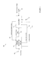
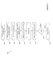
- a method 600 for operation of a voltage inverter includes a voltage converter circuit, a controller and a voltage source supplying input voltage u 0 .
- the method begins at step 602 where a desired output function y 0 (t) is defined and received into the controller.
- a set of circuit parameters for the voltage converter circuit are determined including a load resistance and a set of state variables are measured including the output voltage and the inductor current.
- an initial controller gain k is set to a pre-defined (proportional, integral and derivative) gain value.
- the controller is started, applying the control signal to the voltage converter circuit using the initial duty ratio d and the initial value of desired output voltage y 0 (t).
- the set of circuit parameters and state variables are dynamically measured.
- the duty ratio d is dynamically adjusted based on the set of parameters and the set of state variables, the input voltage u 0 and the controller gain factor k.
- the control signal with duty ratio d is applied to the voltage converter circuit.
- a determination of a stop condition is made. If the stop condition is true, then at step 618 , the voltage converter is stopped. If the stop condition is false, then the method continues performing steps 610 , 612 , 614 and 616 .
- step 612 if the voltage converter circuit is a buck converter then Eqs. 9-11 are applied to determine the duty ratio d(t).
- step 612 if the voltage converter circuit is a boost converter then Eq. 15 is applied to determine the duty ratio d(t).
- step 612 if the voltage converter circuit is a buck-boost converter then Eq. 19 is applied to determine the duty ratio d(t).
- MIMO control methods with n duty ratios can be applied similar to the disclosure in U.S. Patent Application Publication No. 2012/0139509 incorporated herein by reference. MIMO control methods can be applied to the apparatus of the present disclosure to accomplish multiple output inverters with time varying output voltages generated from one or more input voltages.
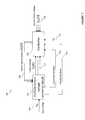
- FIG. 7 shows a preferred embodiment of a tracking inverter 700 suitable for controlling a multiple output voltage converter circuit to produce a set of time varying output voltages.
- Tracking inverter 700 is amenable to input-output linearization methods that do not constrain stability to one operating point, but rather to a set of operating points spanning the expected range of operation during startup and transient modes of operation.
- a multiple output voltage converter circuit 702 is connected to an input voltage 701 (u 0 ) and produces a set of output voltages 710 , [y i (t)], in response to a control signal 709 characterized by a set of duty ratios [d i (t)].
- Set of output voltages 710 are time varying waveforms intended to match a set of desired output voltages 715 , [y 0i (t)], also time varying.
- Controller 720 produces control signal 709 from sensing set of output voltages 710 , input voltage 701 , set of desired output voltages 715 , a set of static circuit parameters 713 including, for example, the load resistances R i , the capacitances C i and the inductances L i of the ith stage of the multiple output voltage converter and a set of state variables 712 including, for example, inductor currents x 1i and capacitor voltages x 2i .
- Control signal 709 determines the states of switch matrix internal to multiple output voltage converter circuit 702 .
- Controller 720 is preferably implemented in one or more digital devices, implemented with programmable software instructions stored in memory and executed by a processor to carry out the converter control functions including output adjustment.
- an analog implementation is used instead of a digital implementation.
- the controller is then implemented as a set of hardware functions, including analog adders and multipliers.
- Controller 720 can implement any desired control method.
- a pulse width modulated (PWM) controller is suitably constructed.
- the PWM controller produces a time varying control signal which drives the switching of each voltage converter stage in the multiple voltage converter circuit with its corresponding duty ratio.
- the controller is implemented according to one of a group of: a discrete electronics circuit; a set of programmed instructions embodied in an FPGA; a set of programmed instructions embodied in a digital signal processor; a microcontroller; a set of programmed instructions embodied in an ASIC; and combinations thereof.
- a suitable hardware platform includes clocking circuits, a CPU, a non-volatile memory for storing the programmed instructions, a volatile memory for storing intermediate results and for storing calculated parameters for the controller and suitable input/output controls for starting, stopping and entering parameters related to the function of the controller.
- the controller is replaced by an analog PID controller with analog inputs for u 0 , y 0 , x 1 , and y.
- the load resistance R and current x 1 is measured and converted to corresponding voltages.
- control method provided by input-output feedback linearization using leading edge modulation with switch off time sampling is meant as an example control method.
- trailing edge modulation with switch off time sampling can be utilized.
- the controller can utilize any control method based on many different control theories.
Landscapes
- Engineering & Computer Science (AREA)
- Power Engineering (AREA)
- Dc-Dc Converters (AREA)
Abstract
Description
{dot over (y)}=a 11 y+a 12 x 1 +b 1 d
{dot over (x)}=a 21 y+a 22 x 1 +b 2 d Eq. 1
y=y
for state variables x1, output voltage y and control signal duty ratio d. It is assumed that the transfer function of Eq. 1 has no pole zero cancellations. The zero z of the transfer function is found by setting the determinant of the matrix
equal to zero and solving for s, with
The solution for the zero z is
the zero of the transfer function of the original system. The general solution with arbitrary constant c1 of the nonhomogeneous equation is
c 1 e zt +x 1p Eq. 6
where x1p is a particular solution of the nonhomogeneous Eq. 1. Assuming that the zero of the system is in the open left plane, i.e. z<0, all solutions converge to a unique particular solution x10 as time t goes to infinity.
where k>0. In another embodiment, integral and derivative gain can also be used to derive d(t). Substituting Eq. 7 into Eq. 1, the following error equations for Δy=(y−y0) and Δx=(x1−x10) are derived as:
which is continuously computed, for the desired voltage y0(t) and the output voltage y, and applied by the controller of
is met where D is a duty ratio for the instantaneous equilibrium point (y=y0′ and x1=x10′) where y0′ and x10′ are constants. Set
where y0(t), {dot over (y)}0(t) are bounded on [0,∞). Substituting d0(t) from Eq. 14 and y=y0 into Eq. 12 results in a differential equation for x1 that has an open left half plane zero as the characteristic root of its linear part
A sufficient condition that a particular solution x10(t) bounded on [0,∞) exists is that y0(t′)=y0′ for a fixed time t′ and the Ridley condition holds for the fixed time t′.
In another embodiment, integral and derivative gain can also be used to derive d(t).
is met where D is a duty ratio for the instantaneous equilibrium point (y=y0′ and x1=x10′) where y0′ and x10′ are constants. A time-varying duty ratio for the desired output voltage y0(t) is given by
for y0(t), {dot over (y)}0(t) bounded on [0,∞). Substituting d0(t) from Eq. 18 and y=y0 into Eq. 16 results in a differential equation for x1 that has an open left half plane zero as the characteristic root of its linear part. A sufficient condition that a particular solution x10(t) bounded on [0,∞) exists is that y0(t′)=y0′ for a fixed time t′ and the Ridley condition holds for the fixed time t′.
In another embodiment, integral and derivative gain can also be utilized to derive d(t).
Claims (30)
Priority Applications (3)
| Application Number | Priority Date | Filing Date | Title |
|---|---|---|---|
| US13/938,333 US9252683B2 (en) | 2009-06-18 | 2013-07-10 | Tracking converters with input output linearization control |
| PCT/US2013/049879 WO2014011738A2 (en) | 2012-07-11 | 2013-07-10 | Tracking converters with input output linearization control |
| US14/465,260 US9369041B2 (en) | 2009-06-18 | 2014-08-21 | Analog input output linearization control |
Applications Claiming Priority (5)
| Application Number | Priority Date | Filing Date | Title |
|---|---|---|---|
| US12/487,242 US8810221B2 (en) | 2009-06-18 | 2009-06-18 | System, method and apparatus for controlling converters using input-output linearization |
| US45885010P | 2010-12-02 | 2010-12-02 | |
| US13/373,673 US8803498B2 (en) | 2009-06-18 | 2011-11-22 | System, apparatus and methods for controlling multiple output converters |
| US201261670520P | 2012-07-11 | 2012-07-11 | |
| US13/938,333 US9252683B2 (en) | 2009-06-18 | 2013-07-10 | Tracking converters with input output linearization control |
Related Parent Applications (1)
| Application Number | Title | Priority Date | Filing Date |
|---|---|---|---|
| US13/373,673 Continuation-In-Part US8803498B2 (en) | 2009-06-18 | 2011-11-22 | System, apparatus and methods for controlling multiple output converters |
Related Child Applications (1)
| Application Number | Title | Priority Date | Filing Date |
|---|---|---|---|
| US14/465,260 Continuation-In-Part US9369041B2 (en) | 2009-06-18 | 2014-08-21 | Analog input output linearization control |
Publications (2)
| Publication Number | Publication Date |
|---|---|
| US20130301321A1 US20130301321A1 (en) | 2013-11-14 |
| US9252683B2 true US9252683B2 (en) | 2016-02-02 |
Family
ID=49548474
Family Applications (1)
| Application Number | Title | Priority Date | Filing Date |
|---|---|---|---|
| US13/938,333 Expired - Fee Related US9252683B2 (en) | 2009-06-18 | 2013-07-10 | Tracking converters with input output linearization control |
Country Status (1)
| Country | Link |
|---|---|
| US (1) | US9252683B2 (en) |
Cited By (1)
| Publication number | Priority date | Publication date | Assignee | Title |
|---|---|---|---|---|
| US20150160975A1 (en) * | 2013-12-09 | 2015-06-11 | Advanced Micro Devices, Inc. | Voltage droop mitigation in 3d chip system |
Families Citing this family (6)
| Publication number | Priority date | Publication date | Assignee | Title |
|---|---|---|---|---|
| US9369041B2 (en) | 2009-06-18 | 2016-06-14 | Cirasys, Inc. | Analog input output linearization control |
| US9252683B2 (en) | 2009-06-18 | 2016-02-02 | Cirasys, Inc. | Tracking converters with input output linearization control |
| US8810221B2 (en) | 2009-06-18 | 2014-08-19 | The Board Of Regents, The University Of Texas System | System, method and apparatus for controlling converters using input-output linearization |
| EP2795419A4 (en) | 2011-12-20 | 2015-07-29 | Cirasys Inc | System and method for controlling output ripple of dc-dc converters with leading edge modulation control using current injection |
| WO2015027081A1 (en) * | 2013-08-23 | 2015-02-26 | Cirasys, Inc. | Analog input linearization control |
| CN110022073B (en) * | 2019-05-07 | 2024-01-30 | 成都信息工程大学 | AC-AC voltage regulating circuit |
Citations (49)
| Publication number | Priority date | Publication date | Assignee | Title |
|---|---|---|---|---|
| US4630187A (en) | 1985-09-09 | 1986-12-16 | Sperry Corporation | Power converter with duty ratio quantization |
| US4677366A (en) | 1986-05-12 | 1987-06-30 | Pioneer Research, Inc. | Unity power factor power supply |
| US4929882A (en) | 1987-06-23 | 1990-05-29 | National Semiconductor Corporation | Apparatus for converting DC to DC having non-feed back variable hysteretic current-mode control for maintaining approximately constant frequency |
| US5138250A (en) | 1990-06-08 | 1992-08-11 | Alcatel Espace | Method of controlling a chopper regulator and a circuit implementing said method |
| US5311421A (en) | 1989-12-08 | 1994-05-10 | Hitachi, Ltd. | Process control method and system for performing control of a controlled system by use of a neural network |
| US5442534A (en) | 1993-02-23 | 1995-08-15 | California Institute Of Technology | Isolated multiple output Cuk converter with primary input voltage regulation feedback loop decoupled from secondary load regulation loops |
| US5477132A (en) | 1992-01-10 | 1995-12-19 | Space Systems/Loral, Inc. | Multi-sectioned power converter having current-sharing controller |
| US5708433A (en) | 1993-09-02 | 1998-01-13 | Craven; Peter Graham | Digital converter |
| US5804950A (en) | 1996-06-20 | 1998-09-08 | Micro Linear Corporation | Input current modulation for power factor correction |
| US5886586A (en) | 1996-09-06 | 1999-03-23 | The Regents Of The University Of California | General constant frequency pulse-width modulators |
| US5920471A (en) | 1996-08-30 | 1999-07-06 | Sgs-Thomson Microelectronics, Srl | Method and apparatus for automatic average current mode controlled power factor correction without input voltage sensing |
| US5943224A (en) | 1998-04-06 | 1999-08-24 | Lucent Technologies Inc. | Post regulator with energy recovery snubber and power supply employing the same |
| US6084450A (en) | 1997-01-14 | 2000-07-04 | The Regents Of The University Of California | PWM controller with one cycle response |
| US20010030879A1 (en) | 2000-04-04 | 2001-10-18 | Greenfeld Fred F. | DC-to-DC power converter |
| US6366070B1 (en) | 2001-07-12 | 2002-04-02 | Analog Devices, Inc. | Switching voltage regulator with dual modulation control scheme |
| US6407515B1 (en) | 1999-11-12 | 2002-06-18 | Lighting Control, Inc. | Power regulator employing a sinusoidal reference |
| US6462962B1 (en) | 2000-09-08 | 2002-10-08 | Slobodan Cuk | Lossless switching DC-to-DC converter |
| US6545887B2 (en) | 1999-08-06 | 2003-04-08 | The Regents Of The University Of California | Unified constant-frequency integration control of three-phase power factor corrected rectifiers, active power filters and grid-connected inverters |
| US20030090253A1 (en) | 2001-11-13 | 2003-05-15 | Balu Balakrishnan | Method and apparatus for a switch mode power supply that generates a high pulse width modulation while maintaining low noise sensitivity |
| US20030199997A1 (en) | 2002-04-18 | 2003-10-23 | Zhiqiang Gao | Scaling and parameterizing a controller |
| US20030222627A1 (en) | 2002-05-31 | 2003-12-04 | Champion Microelectronic Corp. | Power factor correction with carrier control and input voltage sensing |
| US6674272B2 (en) | 2001-06-21 | 2004-01-06 | Champion Microelectronic Corp. | Current limiting technique for a switching power converter |
| US20050068001A1 (en) * | 2001-11-23 | 2005-03-31 | Danfoss Drives A/S | Frequency converter for different mains voltages |
| US6956360B2 (en) | 2003-03-28 | 2005-10-18 | Tdk Corporation | Switching power supply controller and switching power supply |
| US20050231133A1 (en) * | 2004-03-15 | 2005-10-20 | Color Kinetics Incorporated | LED power control methods and apparatus |
| US20060158910A1 (en) | 2005-01-20 | 2006-07-20 | Board Of Regents, The University Of Texas System | System, method and apparatus for controlling converters using input-output linearization |
| US20060171182A1 (en) * | 2005-01-28 | 2006-08-03 | Kasemsan Siri | Solar array inverter with maximum power tracking |
| US7103425B1 (en) | 1999-01-08 | 2006-09-05 | Lexmark International, Inc. | Method of regulating a target system using a frequency comparison of feedback and reference pulse trains |
| US20070046105A1 (en) | 2005-08-02 | 2007-03-01 | Dell Products L.P. | Information handling system including a power supply unit with a power converter for supplying power to multiple outputs |
| US20070114985A1 (en) * | 2005-11-11 | 2007-05-24 | L&L Engineering, Llc | Non-linear pwm controller for dc-to-dc converters |
| US7239257B1 (en) | 2005-10-03 | 2007-07-03 | Zilker Labs, Inc. | Hardware efficient digital control loop architecture for a power converter |
| US20070236200A1 (en) | 2006-04-07 | 2007-10-11 | L&L Engineering, Llc | Methods and systems for disturbance rejection in dc-to-dc converters |
| US20080100362A1 (en) * | 2006-10-31 | 2008-05-01 | Andrew Roman Gizara | Pulse width modulation sequence maintaining maximally flat voltage during current transients |
| US20080231115A1 (en) * | 2007-03-16 | 2008-09-25 | Gyuha Cho | Multiple-Output DC-DC Converter |
| US7489186B2 (en) | 2006-01-18 | 2009-02-10 | International Rectifier Corporation | Current sense amplifier for voltage converter |
| US7602166B1 (en) | 2005-10-12 | 2009-10-13 | National Semiconductor Corporation | System and method for providing a digital self-adjusting power supply that provides a substantially constant minimum supply voltage with regard to variations of PVT, load, and frequency |
| US20100141225A1 (en) | 2008-08-05 | 2010-06-10 | Intersil Americas Inc. | Active pulse positioning modulator |
| US20100164282A1 (en) | 2008-12-26 | 2010-07-01 | Richtek Technology Corporation | Multi-output Switching regulator and control method therefor |
| US7812586B2 (en) | 2006-10-20 | 2010-10-12 | International Rectifier Corporation | One cycle control PFC circuit with dynamic gain modulation |
| US20100308026A1 (en) * | 2009-06-03 | 2010-12-09 | Illinois Tool Works Inc. | Welding power supply with digital control of duty cycle |
| US7851941B2 (en) | 2008-06-13 | 2010-12-14 | Broadcom Corporation | Method and system for a multiple output capacitive buck/boost converter |
| US20100320978A1 (en) | 2009-06-18 | 2010-12-23 | Board Of Regents, The University Of Texas System | System, method and apparatus for controlling converters using input-output linearization |
| US8130522B2 (en) | 2007-06-15 | 2012-03-06 | The Regents Of The University Of Colorado, A Body Corporate | Digital power factor correction |
| US20120146596A1 (en) | 2010-12-13 | 2012-06-14 | Hon Hai Precision Industry Co., Ltd. | Voltage converter |
| WO2012091850A1 (en) | 2010-12-02 | 2012-07-05 | Board Of Regents, The University Of Texas System | System, apparatus and methods for controlling multiple output converters |
| US20130181690A1 (en) * | 2012-01-17 | 2013-07-18 | Rendon Holloway | Active droop power supply with improved step-load transient response |
| US20130241513A1 (en) * | 2012-03-19 | 2013-09-19 | Zentrum Mikroelektronik Dresden Ag | Power converter with average current limiting |
| US20130301321A1 (en) | 2009-06-18 | 2013-11-14 | Cirasys, Inc. | Tracking converters with input output linearization control |
| US8674674B1 (en) * | 2010-07-30 | 2014-03-18 | The Board Of Trustees Of The University Of Alabama For And On Behalf Of The University Of Alabama | Power converter with adaptive voltage positioning controller |
-
2013
- 2013-07-10 US US13/938,333 patent/US9252683B2/en not_active Expired - Fee Related
Patent Citations (52)
| Publication number | Priority date | Publication date | Assignee | Title |
|---|---|---|---|---|
| US4630187A (en) | 1985-09-09 | 1986-12-16 | Sperry Corporation | Power converter with duty ratio quantization |
| US4677366A (en) | 1986-05-12 | 1987-06-30 | Pioneer Research, Inc. | Unity power factor power supply |
| US4929882A (en) | 1987-06-23 | 1990-05-29 | National Semiconductor Corporation | Apparatus for converting DC to DC having non-feed back variable hysteretic current-mode control for maintaining approximately constant frequency |
| US5311421A (en) | 1989-12-08 | 1994-05-10 | Hitachi, Ltd. | Process control method and system for performing control of a controlled system by use of a neural network |
| US5138250A (en) | 1990-06-08 | 1992-08-11 | Alcatel Espace | Method of controlling a chopper regulator and a circuit implementing said method |
| US5477132A (en) | 1992-01-10 | 1995-12-19 | Space Systems/Loral, Inc. | Multi-sectioned power converter having current-sharing controller |
| US5442534A (en) | 1993-02-23 | 1995-08-15 | California Institute Of Technology | Isolated multiple output Cuk converter with primary input voltage regulation feedback loop decoupled from secondary load regulation loops |
| US5708433A (en) | 1993-09-02 | 1998-01-13 | Craven; Peter Graham | Digital converter |
| US5804950A (en) | 1996-06-20 | 1998-09-08 | Micro Linear Corporation | Input current modulation for power factor correction |
| US5920471A (en) | 1996-08-30 | 1999-07-06 | Sgs-Thomson Microelectronics, Srl | Method and apparatus for automatic average current mode controlled power factor correction without input voltage sensing |
| US5886586A (en) | 1996-09-06 | 1999-03-23 | The Regents Of The University Of California | General constant frequency pulse-width modulators |
| US6084450A (en) | 1997-01-14 | 2000-07-04 | The Regents Of The University Of California | PWM controller with one cycle response |
| US5943224A (en) | 1998-04-06 | 1999-08-24 | Lucent Technologies Inc. | Post regulator with energy recovery snubber and power supply employing the same |
| US7103425B1 (en) | 1999-01-08 | 2006-09-05 | Lexmark International, Inc. | Method of regulating a target system using a frequency comparison of feedback and reference pulse trains |
| US6545887B2 (en) | 1999-08-06 | 2003-04-08 | The Regents Of The University Of California | Unified constant-frequency integration control of three-phase power factor corrected rectifiers, active power filters and grid-connected inverters |
| US6407515B1 (en) | 1999-11-12 | 2002-06-18 | Lighting Control, Inc. | Power regulator employing a sinusoidal reference |
| US6538905B2 (en) | 2000-04-04 | 2003-03-25 | Artesyn Technologies, Inc. | DC-to-DC power converter including at least two cascaded power conversion stages |
| US20010030879A1 (en) | 2000-04-04 | 2001-10-18 | Greenfeld Fred F. | DC-to-DC power converter |
| US6462962B1 (en) | 2000-09-08 | 2002-10-08 | Slobodan Cuk | Lossless switching DC-to-DC converter |
| US6674272B2 (en) | 2001-06-21 | 2004-01-06 | Champion Microelectronic Corp. | Current limiting technique for a switching power converter |
| US6366070B1 (en) | 2001-07-12 | 2002-04-02 | Analog Devices, Inc. | Switching voltage regulator with dual modulation control scheme |
| US20030090253A1 (en) | 2001-11-13 | 2003-05-15 | Balu Balakrishnan | Method and apparatus for a switch mode power supply that generates a high pulse width modulation while maintaining low noise sensitivity |
| US20050068001A1 (en) * | 2001-11-23 | 2005-03-31 | Danfoss Drives A/S | Frequency converter for different mains voltages |
| US20030199997A1 (en) | 2002-04-18 | 2003-10-23 | Zhiqiang Gao | Scaling and parameterizing a controller |
| US20030222627A1 (en) | 2002-05-31 | 2003-12-04 | Champion Microelectronic Corp. | Power factor correction with carrier control and input voltage sensing |
| US6956360B2 (en) | 2003-03-28 | 2005-10-18 | Tdk Corporation | Switching power supply controller and switching power supply |
| US20050231133A1 (en) * | 2004-03-15 | 2005-10-20 | Color Kinetics Incorporated | LED power control methods and apparatus |
| US20060158910A1 (en) | 2005-01-20 | 2006-07-20 | Board Of Regents, The University Of Texas System | System, method and apparatus for controlling converters using input-output linearization |
| US7482794B2 (en) | 2005-01-20 | 2009-01-27 | Board Of Regents, The University Of Texas System | System, method and apparatus for controlling converters using input-output linearization |
| US20060171182A1 (en) * | 2005-01-28 | 2006-08-03 | Kasemsan Siri | Solar array inverter with maximum power tracking |
| US20070046105A1 (en) | 2005-08-02 | 2007-03-01 | Dell Products L.P. | Information handling system including a power supply unit with a power converter for supplying power to multiple outputs |
| US7239257B1 (en) | 2005-10-03 | 2007-07-03 | Zilker Labs, Inc. | Hardware efficient digital control loop architecture for a power converter |
| US7602166B1 (en) | 2005-10-12 | 2009-10-13 | National Semiconductor Corporation | System and method for providing a digital self-adjusting power supply that provides a substantially constant minimum supply voltage with regard to variations of PVT, load, and frequency |
| US20070114985A1 (en) * | 2005-11-11 | 2007-05-24 | L&L Engineering, Llc | Non-linear pwm controller for dc-to-dc converters |
| US7489186B2 (en) | 2006-01-18 | 2009-02-10 | International Rectifier Corporation | Current sense amplifier for voltage converter |
| US20070236200A1 (en) | 2006-04-07 | 2007-10-11 | L&L Engineering, Llc | Methods and systems for disturbance rejection in dc-to-dc converters |
| US7812586B2 (en) | 2006-10-20 | 2010-10-12 | International Rectifier Corporation | One cycle control PFC circuit with dynamic gain modulation |
| US20080100362A1 (en) * | 2006-10-31 | 2008-05-01 | Andrew Roman Gizara | Pulse width modulation sequence maintaining maximally flat voltage during current transients |
| US20080231115A1 (en) * | 2007-03-16 | 2008-09-25 | Gyuha Cho | Multiple-Output DC-DC Converter |
| US8130522B2 (en) | 2007-06-15 | 2012-03-06 | The Regents Of The University Of Colorado, A Body Corporate | Digital power factor correction |
| US7851941B2 (en) | 2008-06-13 | 2010-12-14 | Broadcom Corporation | Method and system for a multiple output capacitive buck/boost converter |
| US20100141225A1 (en) | 2008-08-05 | 2010-06-10 | Intersil Americas Inc. | Active pulse positioning modulator |
| US20100164282A1 (en) | 2008-12-26 | 2010-07-01 | Richtek Technology Corporation | Multi-output Switching regulator and control method therefor |
| US20100308026A1 (en) * | 2009-06-03 | 2010-12-09 | Illinois Tool Works Inc. | Welding power supply with digital control of duty cycle |
| US20100320978A1 (en) | 2009-06-18 | 2010-12-23 | Board Of Regents, The University Of Texas System | System, method and apparatus for controlling converters using input-output linearization |
| WO2010148066A2 (en) | 2009-06-18 | 2010-12-23 | Board Of Regents, The University Of Texas System | System, method and apparatus for controlling converters using input-output linearization |
| US20130301321A1 (en) | 2009-06-18 | 2013-11-14 | Cirasys, Inc. | Tracking converters with input output linearization control |
| US8674674B1 (en) * | 2010-07-30 | 2014-03-18 | The Board Of Trustees Of The University Of Alabama For And On Behalf Of The University Of Alabama | Power converter with adaptive voltage positioning controller |
| WO2012091850A1 (en) | 2010-12-02 | 2012-07-05 | Board Of Regents, The University Of Texas System | System, apparatus and methods for controlling multiple output converters |
| US20120146596A1 (en) | 2010-12-13 | 2012-06-14 | Hon Hai Precision Industry Co., Ltd. | Voltage converter |
| US20130181690A1 (en) * | 2012-01-17 | 2013-07-18 | Rendon Holloway | Active droop power supply with improved step-load transient response |
| US20130241513A1 (en) * | 2012-03-19 | 2013-09-19 | Zentrum Mikroelektronik Dresden Ag | Power converter with average current limiting |
Non-Patent Citations (26)
| Title |
|---|
| Bodson, et al., "Differential-Geometric Methods for Control of Electric Motors," Int. J. of Robust and Nonlinear Control 8, (1998), pp. 923-954. |
| Cuk, "Modelling, Analysis, and Design of Switching Converters," Dissertation, California Institute of Technology (1977), 317 pages. |
| Ćuk, "Modelling, Analysis, and Design of Switching Converters," Dissertation, California Institute of Technology (1977), 317 pages. |
| Deisch, C.W., "Simple Switching Control Method Changes Power Converter into a Current Source," IEEE Power Electronics Specialists Conference, 1978 Record, pp. 300-306. |
| Hunt, et al., "Design for Multi-Input Nonlinear Systems," Differential Geometric Control Theory, Birkhauser, Boston, R. W. Brockett, R. S. Millman, and H. J. Sussman, Eds., (1983), 268-298. |
| Hunt, L R., et al., "Global Transformations of Nonlinear Systems," IEEE Transactions on Automatic Control, Jan. 1983, 24-31, vol. 28 No. 1. |
| Isidori, A. "Nonlinear Control Systems," 3rd Ed, Springer-Verlag London Limited (1995). |
| Ma, D., et al., "Enabling Power-Efficient DVFS Operations in Silicon," IEEE Circuits and Systems Magazine, First Quarter, 2010, 14-30. |
| Meyer, et al., "Applications of Nonlinear Transformations to Automatic Flight Control," Automatica, 20 (1984), 103-107. |
| Meyer, G., et al., "Nonlinear System Guidance in the Presence of Transmission Zero Dynamics," NASA Technical Memorandum 4661, Jan. 1995. |
| Middlebrook, R., et al., "A General Unified Approach to Modeling Switch-Converter Power Stages," IEEE Power Electronics Specialists Conference Record, Jun. 1976, 73-86. |
| Mitchell, D. M., "DC-DC Switching Regulator Analysis, Reprint Edition," D.M. Mitchell Consultants, McGraw-Hill, Inc. (1988). |
| Ridley, "A New Small-Signal Model for Current-Mode Control," Ph. D. Dissertation, Virginia Polytechnic Institute and State University (1990) 15 pages. |
| Ridley, Ray, "11 Ways to Generate Multiple Outputs," Switching Power Magazine, 2005, 1-12. |
| Sable, Dan M., et al., "Elimination of the Positive Zero in Fixed Frequency Boost and Flyback Converters," Proceedings of 5th IEEE Applied Power Electronics Conference, 1990, 205-211. |
| Sanders, "Nonlinear Control of Switching Power Converters," Ph.D. Dissertation, Massachusetts Institute of Technology (1989) 254 pages. |
| Shortt, Daniel J., "An Improved Switching Converter Model," Ph.D. Dissertation, Virginia Polytechnic Institute and State University (1982). |
| Sira-Ramirez, "Switched Control of Bilinear Converters Via Pseudolinearization," IEEE Transactions on Circuits and Systems, vol. 36, No. 6, Jun. 1989, 8 pages. |
| Sira-Ramirez, et al., "Exact Linearization in Switched Mode DC-to-DC Power Converters," Int. J. Control, 50 (1989), pp. 511-524. |
| Slotine, et al., "Applied Nonlinear Control," Prentice-Hall, Inc., Englewood Cliffs, 1991. |
| Su, et al., "Linear EqUivalents of Nonlinear Time-Varying Systems," International Symposium on Mathematical Theory of Networks and Systems (1981), 119-123. |
| Su, et al., "Robustness in Nonlinear Control," Differential Geometric Control Theory, Birkhauser, Boston, R. W. Brockett, R. S. Millman, and H. J. Sussman, Eds., (1983), 316-337. |
| Su, R., "On the Linear Equivalents of Nonlinear Systems," Systems and Control Letters 2, (1982),48-52. |
| Tang, Wei, "Average Current-Mode Control and Charge Control for PWM Converters," Ph. D. Dissertation, Virginia Polytechnic Institute and State University (1994). |
| Taylor, Robert J., "Feedback Linearization of Fixed Frequency PWM Converters," Ph.D. Dissertation, University of Texas at Dallas, Nov. 2005. |
| Taylor, Robert J., "Feedback Linearization of Fixed Frequency PWM Converters," Revised Ph.D. Dissertation, University of Texas at Dallas, (undated), 174 pages. |
Cited By (3)
| Publication number | Priority date | Publication date | Assignee | Title |
|---|---|---|---|---|
| US20150160975A1 (en) * | 2013-12-09 | 2015-06-11 | Advanced Micro Devices, Inc. | Voltage droop mitigation in 3d chip system |
| US9595508B2 (en) * | 2013-12-09 | 2017-03-14 | Advanced Micro Devices, Inc. | Voltage droop mitigation in 3D chip system |
| US10361175B2 (en) | 2013-12-09 | 2019-07-23 | Advanced Micro Devices, Inc. | Voltage droop mitigation in 3D chip system |
Also Published As
| Publication number | Publication date |
|---|---|
| US20130301321A1 (en) | 2013-11-14 |
Similar Documents
| Publication | Publication Date | Title |
|---|---|---|
| US9252683B2 (en) | Tracking converters with input output linearization control | |
| US9413235B2 (en) | System, method and apparatus for controlling converters using input-output linearization | |
| US9479047B2 (en) | System and method for controlling a power supply with a feed forward controller | |
| US8125805B1 (en) | Switch-mode converter operating in a hybrid discontinuous conduction mode (DCM)/continuous conduction mode (CCM) that uses double or more pulses in a switching period | |
| US7482794B2 (en) | System, method and apparatus for controlling converters using input-output linearization | |
| EP2200163B1 (en) | Method for predictive PWM current control | |
| US11404962B2 (en) | Switched mode power converter that is switched using current thresholds | |
| US11368109B2 (en) | Power conversion system with PWM carrier transition smoothing and autotuning | |
| Repecho et al. | Robust sliding mode control of a DC/DC Boost converter with switching frequency regulation | |
| JP6858725B2 (en) | DC / DC converter and DC / DC converter control method | |
| Jindal et al. | A Comparative analysis of classical Tuning methods of PI controllers on non-ideal Buck Converter | |
| Prasanth et al. | Investigation of four phase interleaved boost converter under open loop and closed loop control schemes for battery charging applications | |
| JP6805201B2 (en) | DC / DC converter and DC / DC converter control method | |
| US9690308B2 (en) | System and method for controlling output ripple of DC-DC converters with leading edge modulation control using current injection | |
| US9369041B2 (en) | Analog input output linearization control | |
| US10638587B2 (en) | Device and method for processing an inductor current | |
| WO2014011738A2 (en) | Tracking converters with input output linearization control | |
| TamalBiswas et al. | Design of PWM-Based Sliding-Mode Control of Boost Converter with Improved Performance | |
| Liu et al. | Modeling and simulation of Parallel Current Mode controlled boost converter | |
| CN113872442B (en) | Buck converter control circuit, buck converter control method, buck converter and electronic device | |
| JP6873357B1 (en) | Multiphase converter controller | |
| JP6984235B2 (en) | Power converter | |
| WO2015027081A1 (en) | Analog input linearization control | |
| He et al. | Small-signal modeling for digital predictive current mode control in CCM | |
| JP3397769B2 (en) | Inverter control device |
Legal Events
| Date | Code | Title | Description |
|---|---|---|---|
| ZAAA | Notice of allowance and fees due |
Free format text: ORIGINAL CODE: NOA |
|
| ZAAB | Notice of allowance mailed |
Free format text: ORIGINAL CODE: MN/=. |
|
| AS | Assignment |
Owner name: CIRASYS, INC., TEXAS Free format text: ASSIGNMENT OF ASSIGNORS INTEREST;ASSIGNOR:HUNT, LOUIS R.;REEL/FRAME:037370/0413 Effective date: 20151228 |
|
| STCF | Information on status: patent grant |
Free format text: PATENTED CASE |
|
| CC | Certificate of correction | ||
| MAFP | Maintenance fee payment |
Free format text: PAYMENT OF MAINTENANCE FEE, 4TH YR, SMALL ENTITY (ORIGINAL EVENT CODE: M2551); ENTITY STATUS OF PATENT OWNER: SMALL ENTITY Year of fee payment: 4 |
|
| FEPP | Fee payment procedure |
Free format text: MAINTENANCE FEE REMINDER MAILED (ORIGINAL EVENT CODE: REM.); ENTITY STATUS OF PATENT OWNER: SMALL ENTITY |
|
| LAPS | Lapse for failure to pay maintenance fees |
Free format text: PATENT EXPIRED FOR FAILURE TO PAY MAINTENANCE FEES (ORIGINAL EVENT CODE: EXP.); ENTITY STATUS OF PATENT OWNER: SMALL ENTITY |
|
| STCH | Information on status: patent discontinuation |
Free format text: PATENT EXPIRED DUE TO NONPAYMENT OF MAINTENANCE FEES UNDER 37 CFR 1.362 |
|
| FP | Lapsed due to failure to pay maintenance fee |
Effective date: 20240202 |