US9249505B2 - Bis(trimethylsilyl) six-membered ring systems and related compounds as reducing agents for forming layers on a substrate - Google Patents
Bis(trimethylsilyl) six-membered ring systems and related compounds as reducing agents for forming layers on a substrate Download PDFInfo
- Publication number
- US9249505B2 US9249505B2 US14/318,501 US201414318501A US9249505B2 US 9249505 B2 US9249505 B2 US 9249505B2 US 201414318501 A US201414318501 A US 201414318501A US 9249505 B2 US9249505 B2 US 9249505B2
- Authority
- US
- United States
- Prior art keywords
- substrate
- vapor
- atom
- reducing agent
- compound
- Prior art date
- Legal status (The legal status is an assumption and is not a legal conclusion. Google has not performed a legal analysis and makes no representation as to the accuracy of the status listed.)
- Active
Links
- 0 C*CCC(CC1)CC1=C Chemical compound C*CCC(CC1)CC1=C 0.000 description 31
- XGEMPXAUDSZZSS-UHFFFAOYSA-N C1=CN=CC=N1.C[Si](C)(C)N1C=CN([Si](C)(C)C)C=C1 Chemical compound C1=CN=CC=N1.C[Si](C)(C)N1C=CN([Si](C)(C)C)C=C1 XGEMPXAUDSZZSS-UHFFFAOYSA-N 0.000 description 1
- MSDWECOANCLVTJ-JYVZIEBPSA-N CC(C)(C)/N=C/C=N/C(C)(C)C.CC(C)(C)N.O=CC=O Chemical compound CC(C)(C)/N=C/C=N/C(C)(C)C.CC(C)(C)N.O=CC=O MSDWECOANCLVTJ-JYVZIEBPSA-N 0.000 description 1
- DJWTXJNWVDKWSD-FYJQHEJDSA-I CC(C)(C)/N=C/C=N/C(C)(C)C.CC(C)(C)N1C=CN(C(C)(C)C)[AlH2]12N(C(C)(C)C)CC=N2C(C)(C)C.CC(C)(C)N1CC=N(C(C)(C)C)[AlH2]1(Cl)Cl.Cl[Al](Cl)Cl Chemical compound CC(C)(C)/N=C/C=N/C(C)(C)C.CC(C)(C)N1C=CN(C(C)(C)C)[AlH2]12N(C(C)(C)C)CC=N2C(C)(C)C.CC(C)(C)N1CC=N(C(C)(C)C)[AlH2]1(Cl)Cl.Cl[Al](Cl)Cl DJWTXJNWVDKWSD-FYJQHEJDSA-I 0.000 description 1
- ISZUFKWDTWQACK-DZWMJEFGSA-K CC(C)(C)/N=C/C=N/C(C)(C)C.CC(C)(C)N1C=CN(C(C)(C)C)[AlH2]12N(C(C)(C)C)CC=N2C(C)(C)C.Cl[Al](Cl)Cl Chemical compound CC(C)(C)/N=C/C=N/C(C)(C)C.CC(C)(C)N1C=CN(C(C)(C)C)[AlH2]12N(C(C)(C)C)CC=N2C(C)(C)C.Cl[Al](Cl)Cl ISZUFKWDTWQACK-DZWMJEFGSA-K 0.000 description 1
- PAAXOCBSELIUDL-WVYITWJGSA-J CC(C)(C)/N=C/C=N/C(C)(C)C.CC(C)(C)N1C=CN(C(C)(C)C)[Ti]12N(C(C)(C)C)C=CN2C(C)(C)C.Cl[Ti](Cl)(Cl)Cl Chemical compound CC(C)(C)/N=C/C=N/C(C)(C)C.CC(C)(C)N1C=CN(C(C)(C)C)[Ti]12N(C(C)(C)C)C=CN2C(C)(C)C.Cl[Ti](Cl)(Cl)Cl PAAXOCBSELIUDL-WVYITWJGSA-J 0.000 description 1
- PKDMPVHPKBLRTH-BXUSNMSOSA-N CC(C)(C)/N=C/C=N/C(C)(C)C.CC(C)(C)N1CC=N(C(C)(C)C)C12N(C(C)(C)C)CC=N2C(C)(C)C.ClCCl Chemical compound CC(C)(C)/N=C/C=N/C(C)(C)C.CC(C)(C)N1CC=N(C(C)(C)C)C12N(C(C)(C)C)CC=N2C(C)(C)C.ClCCl PKDMPVHPKBLRTH-BXUSNMSOSA-N 0.000 description 1
- PUDDKDZXTRHDDC-UHFFFAOYSA-N CC1=CC=CC=C1.[H]C1(C)C=CC([H])(C)C(C)=C1 Chemical compound CC1=CC=CC=C1.[H]C1(C)C=CC([H])(C)C(C)=C1 PUDDKDZXTRHDDC-UHFFFAOYSA-N 0.000 description 1
- YSQKFZPFNGAFQS-UHFFFAOYSA-N [H]C1(C)C=CC([H])(C)C(C)=C1.[H]C1(C)CN(C)(C)[Cu]2(O1)OC([H])(C)CN2(C)C Chemical compound [H]C1(C)C=CC([H])(C)C(C)=C1.[H]C1(C)CN(C)(C)[Cu]2(O1)OC([H])(C)CN2(C)C YSQKFZPFNGAFQS-UHFFFAOYSA-N 0.000 description 1
Images


Classifications
-
- C—CHEMISTRY; METALLURGY
- C07—ORGANIC CHEMISTRY
- C07F—ACYCLIC, CARBOCYCLIC OR HETEROCYCLIC COMPOUNDS CONTAINING ELEMENTS OTHER THAN CARBON, HYDROGEN, HALOGEN, OXYGEN, NITROGEN, SULFUR, SELENIUM OR TELLURIUM
- C07F7/00—Compounds containing elements of Groups 4 or 14 of the Periodic System
- C07F7/02—Silicon compounds
- C07F7/08—Compounds having one or more C—Si linkages
- C07F7/10—Compounds having one or more C—Si linkages containing nitrogen having a Si-N linkage
-
- C—CHEMISTRY; METALLURGY
- C01—INORGANIC CHEMISTRY
- C01B—NON-METALLIC ELEMENTS; COMPOUNDS THEREOF; METALLOIDS OR COMPOUNDS THEREOF NOT COVERED BY SUBCLASS C01C
- C01B33/00—Silicon; Compounds thereof
- C01B33/02—Silicon
- C01B33/021—Preparation
-
- C—CHEMISTRY; METALLURGY
- C01—INORGANIC CHEMISTRY
- C01B—NON-METALLIC ELEMENTS; COMPOUNDS THEREOF; METALLOIDS OR COMPOUNDS THEREOF NOT COVERED BY SUBCLASS C01C
- C01B33/00—Silicon; Compounds thereof
- C01B33/02—Silicon
- C01B33/021—Preparation
- C01B33/023—Preparation by reduction of silica or free silica-containing material
- C01B33/025—Preparation by reduction of silica or free silica-containing material with carbon or a solid carbonaceous material, i.e. carbo-thermal process
-
- C—CHEMISTRY; METALLURGY
- C01—INORGANIC CHEMISTRY
- C01G—COMPOUNDS CONTAINING METALS NOT COVERED BY SUBCLASSES C01D OR C01F
- C01G3/00—Compounds of copper
- C01G3/04—Halides
- C01G3/05—Chlorides
-
- C—CHEMISTRY; METALLURGY
- C07—ORGANIC CHEMISTRY
- C07F—ACYCLIC, CARBOCYCLIC OR HETEROCYCLIC COMPOUNDS CONTAINING ELEMENTS OTHER THAN CARBON, HYDROGEN, HALOGEN, OXYGEN, NITROGEN, SULFUR, SELENIUM OR TELLURIUM
- C07F7/00—Compounds containing elements of Groups 4 or 14 of the Periodic System
- C07F7/02—Silicon compounds
- C07F7/08—Compounds having one or more C—Si linkages
- C07F7/0803—Compounds with Si-C or Si-Si linkages
- C07F7/0805—Compounds with Si-C or Si-Si linkages comprising only Si, C or H atoms
-
- C—CHEMISTRY; METALLURGY
- C07—ORGANIC CHEMISTRY
- C07F—ACYCLIC, CARBOCYCLIC OR HETEROCYCLIC COMPOUNDS CONTAINING ELEMENTS OTHER THAN CARBON, HYDROGEN, HALOGEN, OXYGEN, NITROGEN, SULFUR, SELENIUM OR TELLURIUM
- C07F7/00—Compounds containing elements of Groups 4 or 14 of the Periodic System
- C07F7/02—Silicon compounds
- C07F7/08—Compounds having one or more C—Si linkages
- C07F7/0803—Compounds with Si-C or Si-Si linkages
- C07F7/081—Compounds with Si-C or Si-Si linkages comprising at least one atom selected from the elements N, O, halogen, S, Se or Te
-
- C—CHEMISTRY; METALLURGY
- C23—COATING METALLIC MATERIAL; COATING MATERIAL WITH METALLIC MATERIAL; CHEMICAL SURFACE TREATMENT; DIFFUSION TREATMENT OF METALLIC MATERIAL; COATING BY VACUUM EVAPORATION, BY SPUTTERING, BY ION IMPLANTATION OR BY CHEMICAL VAPOUR DEPOSITION, IN GENERAL; INHIBITING CORROSION OF METALLIC MATERIAL OR INCRUSTATION IN GENERAL
- C23C—COATING METALLIC MATERIAL; COATING MATERIAL WITH METALLIC MATERIAL; SURFACE TREATMENT OF METALLIC MATERIAL BY DIFFUSION INTO THE SURFACE, BY CHEMICAL CONVERSION OR SUBSTITUTION; COATING BY VACUUM EVAPORATION, BY SPUTTERING, BY ION IMPLANTATION OR BY CHEMICAL VAPOUR DEPOSITION, IN GENERAL
- C23C16/00—Chemical coating by decomposition of gaseous compounds, without leaving reaction products of surface material in the coating, i.e. chemical vapour deposition [CVD] processes
- C23C16/06—Chemical coating by decomposition of gaseous compounds, without leaving reaction products of surface material in the coating, i.e. chemical vapour deposition [CVD] processes characterised by the deposition of metallic material
- C23C16/18—Chemical coating by decomposition of gaseous compounds, without leaving reaction products of surface material in the coating, i.e. chemical vapour deposition [CVD] processes characterised by the deposition of metallic material from metallo-organic compounds
-
- C—CHEMISTRY; METALLURGY
- C23—COATING METALLIC MATERIAL; COATING MATERIAL WITH METALLIC MATERIAL; CHEMICAL SURFACE TREATMENT; DIFFUSION TREATMENT OF METALLIC MATERIAL; COATING BY VACUUM EVAPORATION, BY SPUTTERING, BY ION IMPLANTATION OR BY CHEMICAL VAPOUR DEPOSITION, IN GENERAL; INHIBITING CORROSION OF METALLIC MATERIAL OR INCRUSTATION IN GENERAL
- C23C—COATING METALLIC MATERIAL; COATING MATERIAL WITH METALLIC MATERIAL; SURFACE TREATMENT OF METALLIC MATERIAL BY DIFFUSION INTO THE SURFACE, BY CHEMICAL CONVERSION OR SUBSTITUTION; COATING BY VACUUM EVAPORATION, BY SPUTTERING, BY ION IMPLANTATION OR BY CHEMICAL VAPOUR DEPOSITION, IN GENERAL
- C23C16/00—Chemical coating by decomposition of gaseous compounds, without leaving reaction products of surface material in the coating, i.e. chemical vapour deposition [CVD] processes
- C23C16/44—Chemical coating by decomposition of gaseous compounds, without leaving reaction products of surface material in the coating, i.e. chemical vapour deposition [CVD] processes characterised by the method of coating
- C23C16/455—Chemical coating by decomposition of gaseous compounds, without leaving reaction products of surface material in the coating, i.e. chemical vapour deposition [CVD] processes characterised by the method of coating characterised by the method used for introducing gases into reaction chamber or for modifying gas flows in reaction chamber
- C23C16/45523—Pulsed gas flow or change of composition over time
- C23C16/45525—Atomic layer deposition [ALD]
- C23C16/45553—Atomic layer deposition [ALD] characterized by the use of precursors specially adapted for ALD
-
- C—CHEMISTRY; METALLURGY
- C01—INORGANIC CHEMISTRY
- C01P—INDEXING SCHEME RELATING TO STRUCTURAL AND PHYSICAL ASPECTS OF SOLID INORGANIC COMPOUNDS
- C01P2002/00—Crystal-structural characteristics
- C01P2002/70—Crystal-structural characteristics defined by measured X-ray, neutron or electron diffraction data
- C01P2002/72—Crystal-structural characteristics defined by measured X-ray, neutron or electron diffraction data by d-values or two theta-values, e.g. as X-ray diagram
-
- C—CHEMISTRY; METALLURGY
- C01—INORGANIC CHEMISTRY
- C01P—INDEXING SCHEME RELATING TO STRUCTURAL AND PHYSICAL ASPECTS OF SOLID INORGANIC COMPOUNDS
- C01P2002/00—Crystal-structural characteristics
- C01P2002/80—Crystal-structural characteristics defined by measured data other than those specified in group C01P2002/70
- C01P2002/85—Crystal-structural characteristics defined by measured data other than those specified in group C01P2002/70 by XPS, EDX or EDAX data
-
- C—CHEMISTRY; METALLURGY
- C01—INORGANIC CHEMISTRY
- C01P—INDEXING SCHEME RELATING TO STRUCTURAL AND PHYSICAL ASPECTS OF SOLID INORGANIC COMPOUNDS
- C01P2004/00—Particle morphology
- C01P2004/01—Particle morphology depicted by an image
- C01P2004/03—Particle morphology depicted by an image obtained by SEM
-
- C—CHEMISTRY; METALLURGY
- C01—INORGANIC CHEMISTRY
- C01P—INDEXING SCHEME RELATING TO STRUCTURAL AND PHYSICAL ASPECTS OF SOLID INORGANIC COMPOUNDS
- C01P2004/00—Particle morphology
- C01P2004/01—Particle morphology depicted by an image
- C01P2004/04—Particle morphology depicted by an image obtained by TEM, STEM, STM or AFM
-
- Y—GENERAL TAGGING OF NEW TECHNOLOGICAL DEVELOPMENTS; GENERAL TAGGING OF CROSS-SECTIONAL TECHNOLOGIES SPANNING OVER SEVERAL SECTIONS OF THE IPC; TECHNICAL SUBJECTS COVERED BY FORMER USPC CROSS-REFERENCE ART COLLECTIONS [XRACs] AND DIGESTS
- Y10—TECHNICAL SUBJECTS COVERED BY FORMER USPC
- Y10T—TECHNICAL SUBJECTS COVERED BY FORMER US CLASSIFICATION
- Y10T137/00—Fluid handling
- Y10T137/8593—Systems
Definitions
- the present invention is related to the formation of metal films from “metalorganic” precursors and a reducing agent.
- Atomic layer deposition is a thin film deposition technique that addresses many of the current technological demands.
- ALD affords inherently conformal coverage and sub-nanometer film thickness control due to its self-limited growth mechanism.
- a substrate is contacted with a first chemical composition that modifies the substrate for a first predetermined period of time (a pulse).
- a pulse Such modification involves adsorption to the surface of the substrate, reaction with the surface of the substrate, or a combination of adsorption and reaction.
- a purging gas is introduced to remove any lingering first gaseous chemical composition in the vicinity of the substrate.
- a second gaseous chemical composition that reacts with the modified substrate surface is introduced for a second predetermined period of time into the vicinity of the substrate to form a portion of the thin film.
- a purging gas is subsequently introduced to remove any lingering second chemical composition in the vicinity of the substrate.
- the present invention solves one or more problems of the prior art by providing, in at least one embodiment, a method of reducing a compound having an atom in an oxidized state.
- the method includes a step of reacting a first compound having an atom in an oxidized state with a reducing agent to form a second compound having the atom in a reduced state relative to the first compound.
- the atom in an oxidized state is selected from the group consisting of Groups 2-12 of the Periodic Table, the lanthanides, As, Sb, Bi, Te, Si, Ge, Sn, and Al.
- the reducing agent is selected from the group consisting of compounds described by formulae IA and IB:
- X 1 is CR 6 (SiR 1 R 1′ R 1′′ ) or N(SiR 1 R 1′ R 1′′ );
- X 2 is CR 7 (SiR 1 R 1′ R 1′′ ) or N(SiR 1 R 1′ R 1′′ );
- R 1 , R 1′ , R 1′′ , R 2 , R 3 , R 4 , R 5 , R 6 , and R 7 are each independently H, C 1-10 alkyl, C 6-14 aryl, or C 4-14 heteroaryl.
- a method of reducing a compound having an atom in an oxidized state using gas phase reactants includes a step of providing a vapor of first compound.
- the atom in an oxidized state is selected from the group consisting of Groups 2-12 of the Periodic Table, the lanthanides, As, Sb, Bi, Te, Si, Ge, Sn, and Al.
- the method also includes a step of providing a vapor of a reducing agent.
- the reducing agent is selected from the group consisting of compounds described by formulae IA and IB:
- X 1 is CR 6 (SiR 1 R 1′ R 1′′ ) or N(SiR 1 R 1′ R 1′′ );
- X 2 is CR 7 (SiR 1 R 1′ R 1′′ ) or N(SiR 1 R 1′ R 1′′ );
- R 1 , R 1′ , R 1′′ , R 2 , R 3 , R 4 , R 5 , R 6 , and R 7 are each independently H, C 1-10 alkyl, C 6-14 aryl, or C 4-14 heteroaryl.
- a method of forming a layer by an ALD process includes a step of contacting a substrate with a vapor of a first compound having an atom in an oxidized state to form a first modified surface.
- the atom in an oxidized state is selected from the group consisting of Groups 2-12 of the Periodic Table, the lanthanides, As, Sb, Bi, Te, Si, Ge, Sn, and Al.
- the first modified surface is optionally contacted with an acid for a second predetermined pulse time to form a second modified surface.
- the first modified surface or the second modified surface is contacted with a reducing agent for a third predetermined pulse time to form the layer on the substrate.
- the reducing agent is selected from the group consisting of:
- X 1 is CR 6 (SiR 1 R 1′ R 1′′ ) or N(SiR 1 R 1′ R 1′′ );
- X 2 is CR 7 (SiR 1 R 1′ R 1′′ ) or N(SiR 1 R 1′ R 1′′ );
- R 1 , R 1′ , R 1′′ , R 2 , R 3 , R 4 , R 5 , R 6 , and R 7 are each independently H, C 1-10 alkyl, C 6-14 aryl, or C 4-14 heteroaryl.
- a method for forming a metal includes a step of contacting a metal-containing compound having at least one diazabutadiene ligand, the metal-containing compound having formula III or IV:
- M is a transition metal selected from groups 3-10 of the periodic table, Ru, Pd, Pt, Rh, Ir, Mg, Al, Sn, or Sb;
- R 8 is C 1 -C 12 alkyl, amino (i.e., —NH 2 ), or C 6 -C 18 aryl;
- R 9 is hydrogen, C 1 -C 10 alkyl, C 6 -C 18 aryl, amino, C 1 -C 12 alkylamino, or C 2 -C 22 dialkylamino; and
- X is Cl, Br, or I.
- a method for depositing a thin metal film on a surface of a substrate includes a step of contacting the substrate with a vapor of a metal-containing compound having formula III or IV to form a modified surface on the substrate:
- M is a transition metal selected from groups 3-10 of the periodic table, Ru, Pd, Pt, Rh, Ir, Mg, Al, Sn, or Sb;
- R 8 is C 1 -C 12 alkyl, amino (i.e., —NH 2 ), or C 6 -C 18 aryl;
- R 9 is hydrogen, C 1 -C 10 alkyl, C 6 -C 18 aryl, amino, C 1 -C 12 alkylamino, or C 2 -C 22 dialkylamino; and
- X is Cl, Br, or I.
- the modified surface is then contacted with a vapor of an activating compound to form at least a portion of the thin film on the surface of the substrate.
- the activating compound is an acid or a diketone at a sufficient temperature to form a metal film.
- a method for depositing a thin metal film on a surface of a substrate includes a step of contacting the substrate with a vapor of a metal-containing compound having formula III or IV to form a first modified surface on the substrate:
- M is a transition metal selected from groups 3-10 of the periodic table, Ru, Pd, Pt, Rh, Ir, Mg, Al, Sn, or Sb;
- R 8 is C 1 -C 12 alkyl, amino (i.e., —NH 2 ), or C 6 -C 18 aryl;
- R 9 is hydrogen, C 1 -C 10 alkyl, C 6 -C 18 aryl, amino, C 1 -C 12 alkylamino, or C 2 -C 22 dialkylamino; and
- X is Cl, Br, or I.
- the first modified surface is then contacted with a vapor of an activating compound to form a second modified surface. Characteristically, the activating compound is an acid or a diketone.
- the second modified surface is then contacted with a reducing agent having formula IA or IB to form at least a portion of a metal film on the substrate.
- FIG. 1 provides additional examples of reducing agents encompassed by the present invention
- FIG. 2A is a schematic flowchart illustrating an ALD deposition process using the bis(trimethylsilyl) six-membered ring systems of an embodiment of the invention
- FIG. 2B is a schematic flowchart illustrating an ALD deposition process using the bis(trimethylsilyl) six-membered ring systems of an embodiment of the invention
- FIG. 2C is a schematic flowchart illustrating an ALD deposition process using the bis(trimethylsilyl) six-membered ring systems of an embodiment of the invention
- FIG. 2D is a schematic illustration of an ALD deposition system used in an embodiment of the present invention.
- FIG. 2E is a schematic cross-section of a vapor source containing the reducing agents
- FIG. 3 provides examples of acids that can be reacted with the compounds of formula I
- FIG. 4 provides X-ray diffraction spectra showing CuCl formed by the solution reductions of CuCl 2 and CuCl 2 .H 2 O by 1,4-bis(trimethylsilyl)-2-methyl-1,4-cyclohexadiene;
- FIG. 5 provides an X-ray diffraction spectrum showing copper metal formed by the solution reduction of CuCl 2 to CuCl by 1,4-bis(trimethylsilyl)-2-methyl-1,4-cyclohexadiene, and the subsequent disproportionation to copper metal by ethylenediamine;
- FIG. 6 provides a scanning electron micrograph of a copper film ( ⁇ 8 nm) on a ruthenium-coated (5 nm) SiO 2 wafer;
- FIG. 7 provides a cyclic voltammogram of pyrazine referenced to Ag/AgNO 3 ;
- FIG. 8 provides an X-ray diffraction spectrum showing copper metal formed by the solution reduction of Cu(tmhd) 2 by 1,4-bis(trimethylsilyl)-1,4-dihydropyrazine;
- FIG. 9 provides a cross-sectional SEM micrograph of a copper film on a SiH substrate formed from Cu(dmap) 2 ;
- FIG. 10 provides a top-down SEM micrograph of a copper film on Co/SiO 2 formed from Cu(dmap) 2 ;
- FIG. 11 provides XPS survey scans of a 51 nm copper film deposited on SiH at 150° C. formed from Cu(dmap) 2 ;
- FIG. 12 provides an XPS high-resolution multiplex of the Cu 2p3 region of a film formed from Cu(dmap) 2 ;
- FIG. 13 provides a cross-sectional SEM micrograph of a nickel film on a Si(100) substrate formed from Ni(dmap) 2 ;
- FIG. 14 provides a cross-sectional SEM micrograph of a nickel film on a Ru/SiO 2 substrate formed from Ni(dmap) 2 ;
- FIG. 15 provides XPS survey scans of a 32 nm nickel film deposited on Pd at 150° C. formed from Ni(dmap) 2 ;
- FIG. 16 provides an XPS high-resolution multiplex of the Ni 2p3 region of a film formed from Ni(dmap) 2 ;
- FIG. 17 provides a cross-sectional SEM micrograph of a chromium film on a Ru/SiO 2 substrate formed from Cr(dad tBu2 ) 2 ;
- FIG. 18 provides a cross-sectional SEM micrograph of chromium film on a SiO 2 substrate formed from Cr(dad tBu2 ) 2 ;
- FIG. 19 provides XPS survey scnas of a 124 nm thick chromium film deposited on thermal SiO 2 at 225° C. formed from Cr(dad tBu2 ) 2 ;
- FIG. 20 provides an XPS high-resolution multiplex of the Cr 2p3 region of a film formed from Cr(dad tBu2 ) 2 ;
- FIG. 21 provides a cross-sectional SEM micrograph of a manganese film on a Ru/SiO 2 substrate formed from Mn(dad tBu2 ) 2 ;
- FIG. 22 provides a top-down SEM micrograph of a manganese film on a Ru/SiO 2 substrate formed from Mn(dad tBu2 ) 2 ;
- FIG. 23 provides XPS survey scans of a 27 nm manganese film deposited on SiO 2 at 225° C. formed from Mn(dad tBu2 ) 2 ;
- FIG. 24 provides an XPS high-resolution multiplex of the Mn 2p3 region of a film formed from Mn(dad tBu2 ) 2 ;
- FIG. 25 provides a cross-sectional SEM micrograph of an iron film on a thermal SiO 2 substrate formed from Fe(dad tBu2 ) 2 ;
- FIG. 26 provides a top-down SEM micrograph of an iron film on thermal SiO 2 formed from Fe(dad tBu2 ) 2 ;
- FIG. 27 provides XPS survey scans of a 35 nm thick iron film deposited on Ru/SiO 2 at 225° C. formed from Fe(dad tBu2 ) 2 ;
- FIG. 28 provides an XPS high-resolution multiplex of the Fe 2p3 region of a film formed from Fe(dad tBu2 ) 2 ;
- FIG. 29 provides a cross-sectional SEM micrograph of a cobalt film on a Ru/SiO 2 substrate formed from Co(dad tBu2 ) 2 ;
- FIG. 30 provides a top-down SEM micrograph of a cobalt film on a thermal SiO 2 substrate formed from Co(dad tBu2 ) 2 ;
- FIG. 31 provides XPS survey scans of a 24 nm thick cobalt film deposited on Ru/SiO 2 at 180° C. from Co(dad tBu2 ) 2 ;
- FIG. 32 provides an XPS high-resolution multiplex of the Co 2p3 region of a film formed from Co(dad tBu2 ) 2 ;
- FIG. 33 provides an X-ray diffraction spectrum of showing cobalt metal on a SiO 2 substrate formed from Co(dad tBu2 ) 2 ;
- FIG. 34 provides a cross-sectional SEM micrograph of a nickel film on a Ru/SiO 2 substrate formed from Ni(dad tBu2 ) 2 ;
- FIG. 35 provides a top-down SEM micrograph of a nickel film on a copper substrate formed from Ni(dad tBu2 ) 2 ;
- FIG. 36 provides XPS survey scans of a 34 nm thick nickel film deposited on Ru/SiO 2 at 180° C. from Ni(dad tBu2 ) 2 ;
- FIG. 37 provides an XPS high-resolution multiplex of the Ni 2p3 region for a film formed from Ni(dad tBu2 ) 2 ;
- FIG. 38 provides X-ray diffraction (XRD) spectra for solution reaction precipitates formed from the reaction with titanium tetrachloride and CHD (e.g., formula IA) and titanium tetrachloride and DHP (e.g., formula IB);
- XRD X-ray diffraction
- FIG. 39A provides an SEM cross-section for an ALD film deposited on a platinum substrate from the reaction with titanium tetrachloride and CHD at 180° C.;
- FIG. 39B provides an SEM cross-section for an ALD film deposited on a silicon substrate with a thermal silicon oxide layer from the reaction with titanium tetrachloride and CHD at 180° C.;
- FIG. 39C provides an SEM cross-section for an ALD film deposited on a palladium substrate from the reaction with titanium tetrachloride and CHD at 180° C.;
- FIG. 39D provides an SEM cross-section for an ALD film deposited on a cobalt substrate from the reaction with titanium tetrachloride and CHD at 180° C.;
- FIG. 40 provides XPS survey scans for an ALD film deposited on a platinum substrate from the reaction with titanium tetrachloride and CHD at 180° C.;
- FIG. 41 provides XPS multiplex scans for an ALD film deposited on a platinum substrate from the reaction with titanium tetrachloride and CHD at 180° C.;
- FIG. 42 provides XPS survey scans for ALD film deposited on a silicon substrate with a thermal silicon oxide layer from the reaction with titanium tetrachloride and CHD at 180° C.;
- FIG. 43 provides XPS multiplex scans for an ALD film deposited on silicon substrate with a thermal silicon oxide layer from the reaction with titanium tetrachloride and CHD at 180° C.;
- FIG. 44A provides an SEM cross-section for an ALD film deposited on a platinum substrate from the reaction with titanium tetrachloride and DHP;
- FIG. 44B provides an SEM cross-section for an ALD film on a silicon substrate with a thermal silicon oxide layer from the reaction with titanium tetrachloride and DHP;
- FIG. 44C provides an SEM cross-section for an ALD film on a palladium substrate from the reaction with titanium tetrachloride and DHP;
- FIG. 44D provides an SEM cross-section for an ALD film on a cobalt substrate from the reaction with titanium tetrachloride and DHP;
- FIG. 45 provides X-ray diffraction (XRD) spectra for ALD films formed from the reaction with titanium tetrachloride and DHP on a platinum substrate and a silicon oxide substrate;
- XRD X-ray diffraction
- FIG. 46 provides Energy-dispersive X-ray (EDS) spectra for ALD films formed from the reaction with titanium tetrachloride and DHP on a platinum substrate and a silicon oxide substrates;
- EDS Energy-dispersive X-ray
- FIG. 47 provides XPS survey scans for an ALD film deposited on a platinum substrate from the reaction with titanium tetrachloride and DHP at 100° C.;
- FIG. 48 provides XPS multiplex scans for an ALD film deposited on a platinum substrate from the reaction with titanium tetrachloride and DHP at 100° C.;
- FIG. 49 provides XPS survey scans for an ALD film deposited a silicon substrate with a thermal silicon oxide layer from the reaction with titanium tetrachloride and DHP at 100° C.;
- FIG. 50 provides XPS multiplex scans for an ALD film deposited on a silicon substrate with a thermal silicon oxide layer from the reaction with titanium tetrachloride and DHP at 100° C.;
- FIG. 51A provides a SEM cross-section of an aluminum film deposited on a silicon substrate with a thermal silicon oxide layer from trimethylaluminum and DHP at 180° C.;
- FIG. 51B provides a SEM cross-section of an aluminum film deposited on a cobalt-coated silicon substrate from trimethylaluminum and DHP at 180° C.;
- FIG. 52 provides XPS survey scans for an ALD film deposited on a cobalt-coated silicon substrate from trimethylaluminum and DHP at 180° C.;
- FIG. 53 provides XPS multiplex scans for an ALD film deposited on a cobalt-coated silicon substrate from trimethylaluminum and DHP at 180° C.;
- FIG. 54A provides an SEM cross-section for an ALD film deposited on a platinum substrate from antimony trichloride and DHP at 180° C.;
- FIG. 54B provides an SEM top-down view for an ALD film deposited on a platinum substrate from antimony trichloride and DHP at 180° C.;
- FIG. 54C provides an SEM cross-section for an ALD film deposited on a palladium substrate from antimony trichloride and DHP at 180° C.;
- FIG. 54D provides an SEM top-down view for an ALD film deposited on a palladium substrate from antimony trichloride and DHP at 180° C.;
- FIG. 55 provides XPS survey scans for an ALD film deposited on a palladium substrate from antimony trichloride and DHP at 180° C.;
- FIG. 56 provides XPS multiplex scans for an ALD film deposited on a palladium substrate from antimony trichloride and DHP at 180° C.;
- FIG. 57 provides sheet resistances for cobalt films grown on Ru, Pt, and Pd substrates
- FIG. 58 provides growth rates and sheet resistances versus temperature for cobalt films on a Ru substrate
- FIG. 59 provides SEM cross-sectional micrographs of cobalt films on Ru substrates
- FIG. 60 provides SEM cross-sectional micrographs of cobalt films on Ru substrates
- FIG. 61 provides SEM top-down view micrographs of cobalt films on Ru substrates
- FIG. 62 provides SEM top-down view micrographs of cobalt films on Ru substrates
- FIG. 63A provides a TEM image_of methanol-washed un-capped Si particles
- FIG. 63B provides a TEM image of methanol-washed un-capped Si particles
- FIG. 64 provides an EDS analysis of methanol-washed Si particles
- FIG. 65 provides a PXRD spectrum of Si particles
- FIG. 66A provides a TEM image of Si particles
- FIG. 66B provides a size distribution of Si particles
- FIG. 67A provides a TEM image of Si particles in which methanol was added before reaction with 1-octanol
- FIG. 67B provides a TEM image of Si particles in which methanol was added before reaction with 1-octanol
- FIG. 68 provides the PXRD spectrum of the formed Ge particles.
- FIG. 69 provides a TEM image of the Ge nanoparticles. Since the samples were handled outside after isolation, it is believed that the lighter area around the nanoparticles may be due to the surface oxidation.
- R groups include H, C 1-10 alkyl, C 2-10 alkenyl, C 6-14 aryl (e.g., phenyl, halo, or C 4-14 heteroaryl; the description of a group or class of materials as suitable or preferred for a given purpose in connection with the invention implies that mixtures of any two or more of the members of the group or class are equally suitable or preferred; description of constituents in chemical terms refers to the constituents at the time of addition to any combination specified in the description, and does not necessarily preclude chemical interactions among the constituents of a mixture once mixed; the first definition of an acronym or other abbreviation applies to all subsequent uses herein of the same abbreviation and applies mutatis mutandis to normal grammatical variations of the initially defined abbreviation; and, unless expressly stated to the contrary, measurement of a property is determined by the same technique as previously or later referenced for the same property.
- standard electrode potential means the electrical potential (i.e., the voltage developed) of a reversible electrode at standard state in which solutes are at an effective concentration of 1 mol/liter, the activity for each pure solid, pure liquid, or for water (solvent) is 1, the pressure of each gaseous reagent is 1 atm., and the temperature is 25° C. Standard electrode potentials are reduction potentials.
- a method of reducing a compound having an atom in an oxidized state is provided.
- the method is particularly suited for forming metal-containing layers (e.g., metal layers) by ALD and by chemical vapor deposition (CVD).
- the method includes a step of reacting a first compound having an atom in an oxidized state with a reducing agent to form a second compound having the atom in a reduced state relative to the first compound.
- the atom in an oxidized state is selected from the group consisting of Groups 2-12 of the Periodic Table, the lanthanides, As, Sb, Bi, Te, Si, Ge, Sn, and Al.
- the atom in an oxidized state includes atoms from this group having a standard electrode potential greater than ⁇ 2.4 V relative to a reference electrode potential (e.g., standard hydrogen electrode or a standard Ag/AgNO 3 electrode).
- a reference electrode potential e.g., standard hydrogen electrode or a standard Ag/AgNO 3 electrode.
- such atoms are selected from the group consisting of Groups 3-12 of the Periodic Table, the lanthanides, As, Sb, Bi, Te, Si, Ge, Sn, and Al.
- M is a transition metal.
- M examples include, but are not limited to, Cu, Ni, Co, Cr, Mn, Fe, W, Mo, Ti, Zr, Hf, Rf, V, Nb, Ta, Re, Ru, Rh, Ir, Pd, Pt, and Au. Particularly useful examples for M include, but are not limited to, Cr(II), Mn(II), Fe(II), Co(II), and Ni(II).
- M is a transition metal selected from groups 3-7 of the periodic table.
- the compounds with an atom in an oxidized state include an atom in an oxidation state greater than 0 (e.g., 1, 2, 3, 4, 5, or 6).
- the compounds with an atom in an oxidized state are metal-containing compounds.
- Useful metal-containing compounds are organometallic compounds and metal halides with vapor pressures sufficient for ALD or CVD processes.
- the compounds containing an atom in an oxidized state have vapor pressures of at least 0.01 torr at 100° C.
- the compounds containing an atom in an oxidized state have vapor pressures of at least 0.05 torr to about 700 torr at 100° C.
- the reducing agent is selected from the group consisting of compounds described by formulae IA and IB:
- X 1 is CR 6 (SiR 1 R 1′ R 1′′ ) or N(SiR 1 R 1′ R 1′′ );
- X 2 is CR 7 (SiR 1 R 1′ R 1′′ ) or N(SiR 1 R 1′ R 1′′ );
- R 1 , R 1′ , R 1′′ , R 2 , R 3 , R 4 , R 5 , R 6 , and R 7 are each independently H, C 1-10 alkyl, C 6-14 aryl, or C 4-14 heteroaryl.
- the reducing agent is selected from the group consisting of:
- the compound described by formula IIB is found to be particularly useful in forming metal-containing films.
- Particularly useful examples of the reducing agent are 1,4-bis(trimethylsilyl)-2-methyl-1,4-cyclohexadiene and 1,4-bis(trimethylsilyl)-1,4-dihydropyrazine.
- R 1 , R 1′ , R 1′′ , R 2 , R 3 , R 4 , R 5 , R 6 , and R 7 are each independently H, C 1-10 alkyl, C 6-14 aryl, or C 4-14 heteroaryl.
- R 1 , R 1′ , R 1′′ are each independently C 1-10 alkyl;
- R 2 , R 3 , R 4 , R 5 are each independently H or C 1-10 alkyl; and
- R 6 , and R 7 are H.
- R 1 , R 1′ , R 1′′ are each independently hydrogen, methyl, ethyl, n-propyl, isopropyl, n-butyl, sec-butyl, isobutyl, t-butyl, or phenyl.
- R 2 , R 3 , R 4 , and R 5 are each independently hydrogen, methyl, ethyl, n-propyl, isopropyl, n-butyl, sec-butyl, isobutyl, t-butyl, or phenyl.
- R 6 , R 7 are each independently hydrogen, methyl, ethyl, n-propyl, isopropyl, n-butyl, sec-butyl, isobutyl, t-butyl, or phenyl.
- R 1 , R 1′ , R 1′′ are methyl;
- R 6 , R 7 are hydrogen;
- R 2 , R 3 , R 4 , and R 5 are hydrogen or methyl.
- R 1 , R 1′ , R 1′′ are methyl;
- R 6 , R 7 are hydrogen;
- R 2 , R 3 , R 4 , and R 5 are hydrogen or methyl.
- the first compound includes an atom in an oxidized state selected from Groups 2-12 of the Periodic Table, the lanthanides, As, Sb, Bi, Te, Si, Ge, Sn, and Al.
- the atom in an oxidized state is in an oxidation state of +1, +2, +3, +4, +5, or +6.
- the atom in an oxidized state is a transition metal.
- Particularly useful examples of the atom in an oxidized state include, but are not limited to, Cu, Cr, Mn, Fe, Co, Ti, or Ni.
- ML n ML n Y m wherein M is an atom selected from Groups 2 to 12 of the Periodic Table, As, Sb, Bi, Se, and Te; L is an anionic ligand; n is the number of anionic ligands; Y is a neutral ligand and m is the number of neutral ligands.
- Examples for Y include, but are not limited to, 2,2′-Bipyridine, H 2 O, CH 3 CN, C 5 H 5 N (pyridine), CO, ethylenediamine, 1,10-phenanthroline, PPh 3 , NH 3 , and the like.
- n will be of sufficient number to neutralize any charge on M. In a refinement, n is from 1 to 6 and m is from 1 to 5.
- L examples include optionally-substituted cyclopentadienyl, optionally-substituted ⁇ -diketonates, optionally-substituted amidinates, optionally-substituted guanidinates, optionally-substituted ⁇ -aminoalkoxides, optionally-substituted allyls, and optionally-substituted tris(pyrazolyl)borates.
- the first compound having an atom in an oxidized state is diazadiene compound described by the following formula:
- the activating compound is an acid or a diketone at a sufficient temperature to form a metal film, wherein: M is a transition metal selected from Groups 3-10 of the Periodic Table, Ru, Pd, Pt, Rh, and Ir; In a refinement, M are the atoms in an oxidized state as set forth above; R 8 is C 1 -C 12 alkyl, amino (i.e., —NH 2 ), or C 6 -C 18 aryl; R 9 is hydrogen, C 1 -C 10 alkyl, C 6 -C 18 aryl, amino, C 1 -C 12 alkylamino, or C 2 -C 22 dialkylamino and X is Cl, Br, or I.
- M is a transition metal selected from Groups 3-10 of the Periodic Table, Ru, Pd, Pt, Rh, and Ir
- M are the atoms in an oxidized state as set forth above;
- R 8 is C 1 -C 12 alkyl, amino (i.
- M is Mg, Al, Ti, V, Cr, Mn, Fe, Co, Ni, Cu, Zn, Sn, or Sb.
- M is Cr, Mn, Fe, Ni, Co, Zn, Al, or Mg.
- M is Mg, Al, Sn, or Sb.
- the C 2-5 diketone is a 1,3-diketone. It should be appreciated that the reaction of the present embodiment can be in the gas or liquid phases. In other variations, the reaction is an ALD reaction as set forth below.
- the first compound having an atom in an oxidized state is described by the following formula: M((NR 10 ) 2 ) n wherein: M is a metal selected from Groups 2 to 12 of the Periodic Table, As, Sb, Bi, Se, and Te or the subgroups for the atom in an oxidized state set forth above; R 10 is C 1-6 alkyl, Si(R 11 ) 3 ; R 11 is C 1-6 alkyl, and n is 2, 3, 4, 5, or 6.
- the first compound having an atom in an oxidized state is described by the following formula: M(OR 10 ) n wherein: M is a metal selected from Groups 2 to 12 of the Periodic Table, As, Sb, Bi, Se, and Te or the subgroups for the atom in an oxidized state set forth above; R 10 is C 1-6 alkyl; and n is 2, 3, 4, 5, or 6.
- the first compound having an atom in an oxidized state is ⁇ -diketone compounds described by the following formula:
- M is a metal selected from Groups 2 to 12 of the Periodic Table, As, Sb, Bi, Se, and Te or the subgroups for the atom in an oxidized state set forth above;
- R 12 , R 13 , R 14 are independently H, C 1-10 alkyl, C 1-8 perfluoroalkyl, CF 3 , C 1-10 polyether groups, and the like; and n is 2, 3, 4, 5, or 6.
- the first compound having an atom in an oxidized state is amidinate compounds described by the following formula:
- M is a metal selected from Groups 2 to 12 of the Periodic Table, As, Sb, Bi, Se, and Te or the subgroups for the atom in an oxidized state set forth above;
- R 15 , R 16 , R 17 are independently H, C 1-10 alkyl, C 1-8 perfluoroalkyl, CF 3 , C 1-10 polyether groups, and the like; and n is 2, 3, 4, 5, or 6.
- the compounds including an atom in an oxidized state include, but are not limited to, Ag 2 (tBu 2 -amd) 2 , Al(CH 3 ) 3 , Al(NMe 2 ) 3 , Al 2 (NMe 2 ) 6 , Al 2 (C 2 H 5 ) 4 ( ⁇ -C 2 H 5 ) 2 AlMe 2 (OiPr), Ba(thd) 2 , Ca(tBu 2 amd) 2 , Ce(thd) 4 , Co 2 (CO) 6 (C 2 R 2 ), Co(C 5 H 5 ) 2 , CpCo(CO) 2 , CoCp(C 6 Me 6 ), Co(C 6 Me 6 ) 2 , CpCo(CO) 2 ), Co(acac) 2 , Co(acac) 3 , Co(iPr 2 amd), Co(thd) 3 , Co(thd), Co(tBuEtamd) 2 , Co(tBuEtpmd) 2 , CrCp 2
- Additional examples include, but are not limited to Cp and substituted versions of Ni, Co, Fe, Mn, Cr, Cu alkoxides with beta-amino groups, TiBr 4 , TiI 4 , TiF 4 , halides and pseudohalides of Nb(V), Ta(V), Mo(IV), Mo(V), Mo(VI), W(IV), W(V), W(VI), Al(III), Si(IV), Ge(IV), Ge(II), Sn(II), Sn(IV), Sb(III), Sb(V), Al(NMe 2 ) 3 , volatile Si(IV) compounds, volatile Si(IV) hydrides, volatile Ge(IV) compounds, volatile Ge(IV) hydrides, and halides of Se and Te.
- a method for forming a metal is provided.
- the metal is characterized as having metal atoms in the zero oxidation state.
- the present refinement can be carried out either in solution or in the vapor phase (e.g. ALD, CVD, etc) at temperatures from about 50 to 400° C.
- the metal deposition is carried out at temperatures from about 75 to 200° C.
- a method of forming a metal film by an ALD process comprises a deposition cycle which includes contacting the substrate with vapor of a first compound having an atom in an oxidized state as set forth above such that at least a portion of the vapor of the first compound adsorbs or reacts with a substrate surface to form a modified surface.
- the deposition cycle further includes contacting the modified surface with a vapor of the reducing agents set forth above to react and form at least a portion of the metal film.
- the first compound having an atom in an oxidized state is contacted with the reducing agent at a temperature from about 50 to 400° C.
- the present reaction is used in an ALD process as set forth below.
- step a substrate 10 is contacted with a vapor G1 of a first compound having an atom in an oxidized state to form a first modified surface 12 .
- the atom in an oxidized state is selected from the group consisting Groups 2-12 of the Periodic Table, the lanthanides, As, Sb, Bi, Te, Si, Ge, Sn, and Al.
- the first compound is as set forth above.
- step b) the first modified surface 12 is contacted with a reducing agent G2 for a predetermined pulse time to form layer 14 on the substrate 10 .
- the details of the reducing agent are as set forth above.
- Loop L indicates that steps a), P1), b), and P2) are repeated a plurality of times in order to build up a final layer 16 of predetermined thickness monolayer by monolayer. Additional details of this ALD process are set forth below.
- step a substrate 10 is contacted with a vapor G1 of a first compound having an atom in an oxidized state to form a first modified surface 12 .
- the atom in an oxidized state is selected from the group consisting of Groups 2-12 of the Periodic Table, the lanthanides, As, Sb, Bi, Te, Si, Ge, Sn, and Al
- the first compound is as set forth above.
- step b) the first modified surface 12 is contacted with an acid Al for a second predetermined pulse time to form a second modified surface 12 ′.
- step c) the second modified surface 12 ′ is contacted with a reducing agent G2 for a third predetermined pulse time to form layer 14 on the substrate.
- Purging steps P1, P2, and P3 are performed after steps a), b), and c), respectively.
- Loop L indicates that steps a), P1), b), P2), c), and P3 are repeated a plurality of times in order to build up a final layer 16 of predetermined thickness monolayer by monolayer.
- the details of the reducing agent are as set forth above. Additional details of this ALD process are set forth below.
- deposition system 20 includes reaction chamber 22 , substrate holder 24 , and vacuum pump 26 .
- the substrate is heated via heater 28 .
- the method has a deposition cycle comprising contacting substrate 30 with a vapor of the first compound having an atom in an oxidized state as set forth above.
- the vapor is introduced from precursor source 32 into reaction chamber 22 for a predetermined pulse time.
- the pulse time is controlled via control valve 34 .
- At least a portion of the vapor of the first compound modifies (e.g, adsorbs or reacts with) substrate surface 36 to form a modified surface.
- the method further comprises contacting the modified surface with a vapor of the reducing agent as set forth above from source 40 for a predetermined pulse time controlled by valve 42 .
- the method further comprises removing at least a portion of the vapor of the first compound that is lingering in the gas phase (i.e., has not adsorbed or reacted with the substrate) from the vicinity of the substrate before introducing the vapor of the reducing agent and removing at least a portion of the vapor of the reducing agent from the vicinity of the substrate.
- the metal-containing compound and the reducing agent are removed in purging steps by introducing a purge gas from purge source 44 into reaction chamber 22 for a predetermined purge time. The purge time is controlled by control valve 46 .
- the method further includes at least one additional deposition cycle comprising sequentially contacting the substrate with the vapor of the first compound and then the vapor of the reducing agent.
- the substrate is contacted for a plurality of additional deposition cycles.
- the substrate may be contacted with from 1 to several thousand deposition cycles depending on the thickness of the film desired.
- the substrate is contacted with the vapor of the first compound having an atom in an oxidized state and then the vapor of the reducing agent for 1 to 5000 deposition cycles.
- the substrate is contacted with the vapor of the first compound having an atom in an oxidized state and then the vapor of the reducing agent for 10 to 2000 deposition cycles.
- the substrate is contacted with the vapor of the first compound having an atom in an oxidized state and then the vapor of the reducing agent for 20 to 1000 deposition cycles.
- FIG. 2D uses a source 40 for providing the vapor of a reducing agent.
- FIG. 2E provides a schematic cross-section of such a vapor source.
- Reducing agent source 40 includes vessel 60 and reducing agent 62 which is contained within and held by the vessel.
- Reducing agent 62 is one or more of the reducing agents set forth above.
- reducing agent 62 is described by IA, IB, IIA, IIB, IIC, and IID.
- Valve 64 is attached to vessel 60 .
- Valve 64 prevents escape of the reducing agent when the valve is closed and allows escape (i.e., passage into the ALD reaction chamber 22 through output conduit 66 ) of the reducing agent when the valve is opened.
- source 40 is a bubbler having an input conduit 70 for flowing a gas into vessel 60 and out of output conduit 66 thereby transferring the reducing agent.
- Valve 72 allows input conduit 70 to be opened and closed.
- reducing agent source 40 in a refinement reducing agent source 40 includes fitting 74 positioned outside of and in fluid communication with valve 64 .
- fitting 76 is position outside of and in fluid communication with valve 72 . Fittings 74 and 76 allow attachment of the reducing agent source to ALD or CVD equipment.
- a system and method of forming a metal-containing film is provided.
- the vapor of the first compound having an atom in an oxidized state is introduced from precursor source 32 into reaction chamber 22 for a first predetermined pulse time.
- the first predetermined pulse time should be sufficiently long that available binding sites on the substrate surface (coated with metal layers or uncoated) are saturated (i.e., metal-containing compound attached).
- the first predetermined pulse time is from 1 second to 20 seconds.
- the first predetermined pulse time is controlled via control valve 34 .
- At least a portion of the vapor of the metal-containing compound modifies (e.g, adsorbs or reacts with) substrate surface 36 to form a first modified surface.
- Reaction chamber 22 is then purged with an inert gas from purge source 44 for a first purge time.
- the first purge time is sufficient to remove the metal-containing compound from reaction chamber 22 and is typically from 0.5 seconds to 2 minutes.
- an acid such as formic acid is then introduced from acid source 50 into reaction chamber 22 for a second predetermined pulse time.
- R 20 is H (i.e., hydride), C 1-8 alkyl, C 6-12 aryl, or C 1-8 fluoroalkyl
- X is N 3 ⁇ , NO 3 ⁇
- halide e.g., Cl, F, Br
- o is an integer from 1 to 6.
- R 20 is hydride, C 1-4 alkyl, C 6-10 aryl, or C 1-4 fluoroalkyl
- X is N 3 ⁇ , NO 3 ⁇
- halide e.g., Cl, F, Br
- n is an integer from 1 to 6.
- useful alkyl groups include, but are not limited to, methyl, ethyl, n-propyl, isopropyl, n-butyl, t-butyl, iso-butyl, sec-butyl, and the like.
- useful aryl groups include, but are not limited to, phenyl, tolyl, naphthyl, and the like.
- the second predetermined pulse time is controlled via valve 52 and should be sufficiently long that available binding sites on the first modified substrate surface are saturated and a second modified surface is formed. Typically, the second predetermined pulse time is from 0.1 second to 20 seconds. Reaction chamber 22 is then purged with an inert gas for a second purge time (typically, 0.5 seconds to 2 minutes as set forth above).
- a reducing agent as set forth above is then introduced from reducing agent source 40 into reaction chamber 22 for a third predetermined time controlled by valve 42 .
- the third predetermined pulse time should be sufficiently long that available binding sites on the second modified substrate surface are saturated, with a metal layer being formed thereon.
- the third predetermined pulse time is from 0.1 second to 20 seconds.
- Reaction chamber 22 is then purged with an inert gas for a third purge time (typically, 0.5 second to 2 minutes as set forth above).
- the substrate will be at a temperature suitable to the properties of the chemical precursor(s) and film to be formed.
- the substrate is set to a temperature from about 0 to 1000° C.
- the substrate has a temperature from about 50 to 450° C.
- the substrate has a temperature from about 100 to 250° C.
- the substrate has a temperature from about 150 to 400° C.
- the substrate has a temperature from about 200 to 300° C.
- the pressure during film formation is set at a value suitable to the properties of the chemical precursors and film to be formed.
- the pressure is from about 10 ⁇ 6 Torr to about 760 Torr.
- the pressure is from about 0.1 millitorr to about 10 Torr.
- the pressure is from about 1 to about 100 millitorr.
- the pressure is from about 1 to 20 millitorr.
- Pulse times and purge times also depend on the properties of the chemical precursors and the geometric shape of the substrates. Thin film growth on flat substrates uses short pulse and purge times, but pulse and purge times in ALD growth on 3-dimensional substrates can be very long. Therefore, in one refinement, pulse times and purge times are each independently from about 0.0001 to 200 seconds. In another refinement, pulse and purge times are each independently from about 0.1 to about 10 seconds.
- a method for forming a metal is provided.
- the method of this embodiment is an advancement of the method of U.S. patent application Ser. Nos. 13/818,154 and 13/930,471, the entire disclosures of which are hereby incorporated by reference.
- the method includes a step of contacting a metal-containing compound having at least one diazabutadiene ligand, the metal-containing compound having formula III or IV:
- the activating compound is an acid or a diketone at a sufficient temperature to form a metal film, wherein: M is a transition metal selected from Groups 3-10 of the Periodic Table, Ru, Pd, Pt, Rh, and Ir; R 8 is C 1 -C 12 alkyl, amino (i.e., —NH 2 ), or C 6 -C 18 aryl; R 9 is hydrogen, C 1 -C 10 alkyl, C 6 -C 18 aryl, amino, C 1 -C 12 alkylamino, or C 2 -C 22 dialkylamino and X is Cl, Br, or I.
- M is a transition metal selected from Groups 3-10 of the Periodic Table, Ru, Pd, Pt, Rh, and Ir
- R 8 is C 1 -C 12 alkyl, amino (i.e., —NH 2 ), or C 6 -C 18 aryl
- R 9 is hydrogen, C 1 -C 10 alkyl, C 6 -C 18
- M is Mg, Al, Ti, V, Cr, Mn, Fe, Co, Ni, Cu, Zn, Sn, or Sb.
- M is Cr, Mn, Fe, Ni, Co, Zn, Al, or Mg.
- M is Mg, Al, Sn, or Sb.
- the C 2-5 diketone is a 1,3-diketone. It should be appreciated that the reaction of the present embodiment can be in the gas or liquid phases. In other variations, the reaction is an ALD reaction as set forth below.
- M is a metal, and in particular, a transition metal in a 0, 1+, 2+, 3+, or 4+ oxidation state.
- useful transition metals for M include, but are not limited to, Cu, Ni, Co, Cr, Mn, Fe, W, Mo, Ti, Zr, Hf, Rf, V, Nb, Ta, Re, Ru, Rh, Ir, Pd, Pt, and Au.
- Particularly useful examples for M include, but are not limited to, Cr(II), Mn(II), Fe(II), Co(II), and Ni(II).
- R 8 is a C 1 -C 12 alkyl or C 6 -C 18 aryl.
- R 8 is C 1 -C 4 alkyl.
- Specific examples for R 8 include, but are not limited to, methyl, ethyl, propyl, n-butyl, sec-butyl, isobutyl, t-butyl, and the like.
- R 1 is t-butyl.
- R 8 is C 6 -C 10 aryl.
- specific examples for R 1 include, but are not limited to, phenyl, biphenyl, napthyl, and the like.
- R 1 include substituted variations of such groups.
- substituents include, but are not limited to, halogen, hydroxyl, —NO 2 , and in the case of aryl, C 1 -C 4 alkyl. These substituents are particularly relevant when R 1 is aryl.
- R 9 is C 1 -C 12 alkyl or C 6 -C 18 aryl. In a variation, R 9 is C 1 -C 4 alkyl.
- specific examples for R 8 include, but are not limited to, methyl, ethyl, propyl, n-butyl, sec-butyl, isobutyl, t-butyl, and the like. It should also be appreciated that when R 9 is C 1 -C 12 alkylamino or C 2 -C 22 dialkylamino, the alkyl component is the same as set forth for when R 8 is a C 1 -C 12 alkyl.
- R 9 examples include, but are not limited to, methylamino, ethylamino, propylamino, diethylamino, dimethylamino, dipropylamino, and the like.
- R 9 is C 6 -C 10 aryl.
- specific examples for R 1 include, but are not limited to, phenyl, biphenyl, napthyl, and the like.
- the definitions for R 9 include substituted variations of such groups. Examples of substituents include, but are not limited to, halogen, hydroxyl, —NO 2 , and in the case of aryl, C 1 -C 4 alkyl. These substituents are particularly relevant when R 1 is aryl.
- an activating compound such as an acid.
- Particularly useful activating compounds are C 1-5 organic acids (e.g., C 1-5 carboxylic acids) such as formic acid and C 1-8 diketones. Examples of other suitable acids are provided in FIG. 3 .
- R 20 is H (i.e., hydride), C 1-8 alkyl, C 6-12 aryl, or C 1-8 fluoroalkyl
- X is N 3 ⁇ , NO 3 ⁇
- halide e.g., Cl, F, Br
- n is an integer from 1 to 6.
- R 20 is hydride, C 1-4 alkyl, C 6-10 aryl, or C 1-4 fluoroalkyl
- X is N 3 ⁇ , NO 3 ⁇
- halide e.g., Cl, F, Br
- n is an integer from 1 to 6.
- useful alkyl groups include, but are not limited to, methyl, ethyl, n-propyl, isopropyl, n-butyl, t-butyl, iso-butyl, sec-butyl, and the like.
- useful aryl groups include, but are not limited to, phenyl, tolyl, naphthyl, and the like.
- the diazabutadiene ligand is a radical anion having the following formula:
- the diazabutadiene ligand is a dianion having the following formula:
- the metal-containing compound when M is Al, includes a diazabutadiene ligand that is a radical ion having the following formula:
- step a substrate 10 is contacted with a vapor of a metal-containing compound G1 having formula III or IV to form a modified surface 12 on the substrate 10 .
- the modified surface is then contacted with the activating compound Al to form at least a portion of the metal film on the substrate.
- M is Co, Ni, Cr, Fe, and Mn.
- step a) substrate 10 is contacted with a vapor of a metal-containing compound G1 having formula III or IV to form a first modified surface 12 on the substrate 10 .
- step b) the first modified surface 12 is then contacted with a vapor of the activating compound A1 to form a second modified surface 12 ′.
- step c) the second modified surface 12 ′ is then contacted with the vapor of a reducing agent G2 to form at least a portion of a metal film on the substrate.
- Suitable reducing agents include, but are not limited to, hydrazine, hydrazine hydrate, alkyl hydrazines, 1,1-dialkylhydrazines, 1,2-dialkylhydrazines, H 2 , H 2 plasma, ammonia, ammonia plasma, silanes, disilanes, trisilanes, germanes, diborane, formalin, amine borane, dialkyl zinc, alkyl aluminum, alkyl gallium, alkyl indium complexes, and other plasma-based gases, and combinations thereof.
- Additional examples of reducing agents include the bis(trimethylsilyl) six-membered ring systems and related compounds as set forth above.
- deposition system 20 includes reaction chamber 22 , substrate holder 24 , and vacuum pump 26 .
- the substrate is heated via heater 28 .
- the method has a deposition cycle comprising contacting substrate 30 with a vapor of the compound having formula III or IV or the variations of these compounds as set forth above.
- the vapor is introduced from precursor source 32 into reaction chamber 22 for a predetermined pulse time.
- the pulse time is controlled via control valve 34 .
- At least a portion of the vapor of the compound having formula III or IV modifies (e.g, adsorbs or reacts with) substrate surface 36 to form a modified surface.
- the method further comprises contacting the modified surface with a vapor of the activating compound (e.g., C 1-5 organic acids such as formic acid and C 1-8 diketone) as set forth above from source 50 for a predetermined pulse time to form a metal layer or metal-containing layer.
- a vapor of the activating compound e.g., C 1-5 organic acids such as formic acid and C 1-8 diketone
- the method further comprises removing at least a portion of the vapor of the compound having formula III or IV that is lingering in the gas phase (i.e., has not adsorbed or reacted with the substrate) from the vicinity of the substrate before introducing the vapor of the activating compound and removing at least a portion of the vapor of the activating compound from the vicinity of the substrate.
- the metal-containing compound and the activating compound are removed in purging steps by introducing a purge gas from purge source 44 into reaction chamber 22 for a predetermined purge time. The purge time is controlled by control valve 46 .
- the method further includes at least one additional deposition cycle comprising sequentially contacting the substrate with the vapor of the compound having formula III or IV and then the vapor of the reducing agent.
- the substrate is contacted for a plurality of additional deposition cycles.
- the substrate may be contacted with from 1 to several thousand deposition cycles depending on the thickness of the film desired.
- the substrate is contacted with the vapor of the compound having formula III or IV and then the vapor of the activating compound for 1 to 5000 deposition cycles.
- the substrate is contacted with the vapor of the compound having formula III or IV and then the vapor of the activating compound for 10 to 2000 deposition cycles.
- the substrate is contacted with the vapor of the compound having formula III or IV and then the vapor of the activating compound for 20 to 1000 deposition cycles.
- a method of forming a metal-containing film is provided.
- the vapor of the compound having formula III or IV is introduced from precursor source 32 into reaction chamber 22 for a first predetermined pulse time.
- the first predetermined pulse time should be sufficiently long that available binding sites on the substrate surface (coated with metal layers or uncoated) are saturated (i.e., metal-containing compound attached).
- the first predetermined pulse time is from 1 second to 20 seconds.
- the first predetermined pulse time is controlled via control valve 34 .
- At least a portion of the vapor of the metal-containing compound modifies (e.g, adsorbs or reacts with) substrate surface 36 to form a first modified surface.
- Reaction chamber 22 is then purged with an inert gas from purge gas source 44 for a first purge time.
- the first purge time is sufficient to remove the metal-containing compound from reaction chamber 22 and is typically from 0.5 seconds to 2 minutes.
- the activating compound e.g., C 1-5 organic acids such as formic acid and C 1-8 diketone
- the second predetermined pulse time is controlled via valve 52 and should be sufficiently long that available binding sites on the first modified substrate surface are saturated and a second modified surface is formed.
- the second predetermined pulse time is from 0.1 second to 20 seconds.
- the second predetermined pulse time is controlled via control valve 32 .
- Reaction chamber 12 is then purged with an inert gas for a second purge time (typically, 0.5 seconds to 2 minutes as set forth above).
- a reducing agent having formula IA or IB or the derivatives thereof as set forth above is then introduced from reducing agent source 40 into reaction chamber 22 for a third predetermined time controlled by valve 42 .
- the third predetermined pulse time should be sufficiently long that available binding sites on the second modified substrate surface are saturated, with a metal layer being formed thereon.
- the third predetermined pulse time is from 0.1 second to 20 seconds.
- Reaction chamber 22 is then purged with an inert gas for a third purge time (typically, 0.5 seconds to 2 minutes as set forth above).
- the method further includes at least one additional deposition cycle comprising sequentially contacting the substrate with the vapor of the compound having formula III or IV and then the vapor of the reducing agent.
- the substrate is contacted for a plurality of additional deposition cycles.
- the substrate may be contacted with from 1 to several thousand deposition cycles depending on the thickness of the film desired.
- the substrate is contacted with the vapor of the compound having formula III or IV and then the vapor of the activating compound for 1 to 5000 deposition cycles.
- the substrate is contacted with the vapor of the compound having formula III or IV and then the vapor of the activating compound for 10 to 2000 deposition cycles.
- the substrate is contacted with the vapor of the compound having formula III or IV and then the vapor of the activating compound for 20 to 1000 deposition cycles.
- the substrate will be at a temperature suitable to the properties of the chemical precursor(s) and film to be formed.
- the substrate is set to a temperature from about 0 to 1000° C.
- the substrate has a temperature from about 50 to 450° C.
- the substrate has a temperature from about 100 to 250° C.
- the substrate has a temperature from about 150 to 400° C.
- the substrate has a temperature from about 200 to 300° C.
- the pressure during film formation is set at a value suitable to the properties of the chemical precursors and film to be formed.
- the pressure is from about 10 ⁇ 6 Torr to about 760 Torr.
- the pressure is from about 0.1 millitorr to about 10 Torr.
- the pressure is from about 1 to about 100 millitorr.
- the pressure is from about 1 to 20 millitorr.
- Pulse times and purge times also depend on the properties of the chemical precursors and the geometric shape of the substrates. Thin film growth on flat substrates uses short pulse and purge times, but pulse and purge times in ALD growth on 3-dimensional substrates can be very long. Therefore, in one refinement, pulse times and purge times are each independently from about 0.0001 to 200 seconds. In another refinement, pulse and purge times are each independently from about 0.1 to about 10 seconds.
- Powder and thin film XRD experiments were performed on a Rigaku R200B 12 kW rotating anode diffractometer, using Cu K ⁇ radiation (1.54056 ⁇ ) at 40 kV and 150 mA.
- XPS analysis was performed on a Perkin-Elmer 5500 XPS system using monochromatized Al K ⁇ radiation. AugerScan v3.2 was used as the analysis software. Deposited thin films were exposed to air for several days prior to XPS analysis.
- Scheme 1 illustrates the synthesis of 1,4-bis(trimethylsilyl)-2-methyl-1,4-cyclohexadiene according to a literature procedure (Laguerre, M.; Dunogues, J.; Calas, R.; Duffaut, N. J. Organomet. Chem. 1976, 112, 49-59).
- the air-sensitive product was a clear liquid, and was pure by 1 H NMR.
- Copper metal film growth was attempted by ALD using bis(dimethylaminopropanoxide)copper [Cu(dmap) 2 ] and 1,4-bis(trimethylsilyl)-2-methyl-1,4-cyclohexadiene as reagents.
- Various substrates were tested for film growth, including Si(100), SiH, thermal SiO 2 , Cu, Pt, Pd, TiN, and Ru/SiO 2 .
- Each cycle consisted of a 3.0 s pulse of Cu(dmap) 2 , a 10.0 s purge, a 1.0 s pulse of 1,4-bis(trimethylsilyl)-2-methyl-1,4-cyclohexadiene, and a final 10.0 s purge.
- the 1,4-bis(trimethylsilyl)-2-methyl-1,4-cyclohexadiene bubbler was maintained at 70° C. and the reaction chamber was held at 150° C. After 1,000 cycles, a copper film was clearly observable on the ruthenium substrate. A growth rate of 0.08 ⁇ /cycle was determined after measurement of the film by SEM. Copper metal was not observed on any other substrates.
- Scheme 2 provides a reaction scheme for a two-step ALD process using Cu(dmap) 2 and 1,4-bis(trimethylsilyl)-2-methyl-1,4-cyclohexadiene:
- FIG. 6 provides a scanning electron micrograph of a copper film ( ⁇ 8 nm) on a ruthenium-coated (5 nm) SiO 2 wafer.
- Table 2 shows representative combinations of ring substituents, along with the relative electronic energy differences.
- the structure with three methoxy groups shows the greatest improvement, with ⁇ 3.636 kcal per mole upon aromatization relative to CHD.
- the trimethylsilyl moieties should be highly reactive towards the ligands (e.g. halogens), affording a trimethylsilated ligand byproduct.
- the resulting pyrazine dianion may simultaneously coordinate to the metal cation.
- Subsequent formation of an aromatic pyrazine byproduct may facilitate the reduction to elemental metal.
- Pyrazine has a cathodic potential of ⁇ 2.4 V as measured relative to Ag/AgNO 3 ( FIG. 7 ).
- this approach may enable the thermal reduction of numerous metal precursors that are otherwise unreactive towards conventional coreagents at temperatures suitable for ALD.
- 1,4-bis(trimethylsilyl)-1,4-dihydropyrazine was prepared on a 40 g scale following a literature procedure (Sulzbach, R. A.; Iqbal, A. F. M. Angew. Chem. Int. Ed. Engl. 1971, 10, 127).
- the air-sensitive, yellow solid was purified by sublimation at 80° C./0.05 Torr. Preparative sublimation of the product yielded 97.1% recovery with no residue.
- the thermal decomposition temperature was determined to be greater than 265° C.
- Each deposition cycle consisted of a precursor pulse (3.0 s for M(dmap) 2 and 6.0 s for M(dad tBu2 ) 2 ), a 5.0 s purge, a 0.2 s pulse of formic acid, a 5.0 s purge, a 1.0 s pulse of DHP, and a final 10.0 s purge. Delivery temperatures were maintained at 100° C. and 150° C. for M(dmap) 2 and M(dad tBu2 ) 2 precursors, respectively. Delivery temperatures were maintained at 70° C. and 21° C. for DHP and formic acid, respectively. Selected films from each deposition were characterized by SEM, XRD, and XPS as provided by FIGS. 9-37 .
- Titanium film growth was demonstrated using TiCl 4 +CHD. Each cycle consisted of a 0.2 s pulse of TiCl 4 , a 15.0 s purge, a 1.0 s pulse of CHD, and a 10.0 s purge.
- the TiCl 4 bubbler was maintained at 20° C. and the reaction chamber was held at 180° C.
- the temperature of the solid state booster for CHD delivery was set to 75° C.
- definitive films were observed on Pd, Pt, and SiO 2 with growth rates of approximately 0.09 ⁇ /cycle, 0.15 ⁇ /cycle, and 0.08 ⁇ /cycle, respectively.
- Discontinuous (island-type) growth was observed by SEM on the Co substrate. Faint films were observed on the Ru and Cu substrates; their presence was confirmed by SEM analysis.
- platinum substrates consist of silicon substrates with a thermal oxide over coated with a platinum layer.
- Palladium substrates consist of silicon substrates with a thermal oxide over coated with a palladium layer.
- Cobalt substrates consist of silicon substrates with a thermal oxide over coated with a cobalt layer. It should be appreciated that SEM cross-sections are not able to distinguish the metal coating the substrate and the ALD film deposited thereon.
- FIG. 39A provides an SEM cross-section for an ALD film deposited on a platinum substrate from the reaction with TiCl 4 and CHD at 180° C. From the micrograph, the combined platinum and titanium thickness is about 25 nm with an approximate platinum layer thickness of about 14 to 18 nm and a titanium layer thickness from 7 to 11 nm.
- FIG. 39B provides an SEM cross-section for an ALD film deposited on a silicon substrate with a thermal silicon oxide layer from the reaction with TiCl 4 and CHD at 180° C. From the micrograph, the titanium layer thickness is about 8 nm.
- FIG. 39C provides an SEM cross-section for an ALD film deposited on a palladium substrate from the reaction with titanium tetrachloride and CHD at 180° C.
- the combined palladium and titanium thickness is about 29 nm with an approximate palladium layer thickness of about 12 to 14 nm and a titanium layer thickness from 15 to 17 nm.
- FIG. 39D provides an SEM cross-section for an ALD film deposited on a cobalt substrate from the reaction with titanium tetrachloride and CHD at 180° C. From the micrograph, the combined cobalt and titanium thickness is about 11 nm with an approximate cobalt layer thickness of about 6 to 10 nm and titanium layer thickness of about 1 to 5 nm.
- FIGS. 40 and 41 respectively show XPS survey scans and XPS multiplex scans for an 8 nm ALD film deposited on a platinum substrate by reacting TiCl4 and CHD at 180° C. The scans confirm the presence of a titanium-containing film.
- FIGS. 42 and 43 respectively show XPS survey scans and XPS multiplex scans for an 8 nm ALD film deposited on a silicon oxide coated silicon substrate by reacting TiCl4 and CHD at 180 C. The scans confirm the presence of a titanium-containing film.
- Titanium film growth was demonstrated using TiCl 4 +DHP. Each cycle consisted of a 0.2 s pulse of TiCl 4 , a 15.0 s purge, a 1.0 s pulse of DHP, and a 10.0 s purge.
- the TiCl 4 bubbler was maintained at 20° C. and the reaction chamber was held at 100° C.
- the temperature of the solid state booster for DHP delivery was set to 75° C. After 3,000 cycles, definitive film growth was achieved on Pd, Pt, TiN, Co, Cu, Ru, Si(100), and SiO 2 .
- Average approximate growth rates were determined by SEM analysis: Pd (0.04 ⁇ /cycle), Pt (0.11 ⁇ /cycle), TiN (0.04 ⁇ /cycle), Co (0.13 ⁇ /cycle), Cu (0.11 ⁇ /cycle), Ru (0.08 ⁇ /cycle), Si (0.11 ⁇ /cycle), and SiO 2 (0.12 ⁇ /cycle).
- FIG. 44A provides an SEM cross-section for an ALD film deposited on a platinum substrate from the reaction with titanium tetrachloride and DHP. From the micrograph, the combined platinum and titanium thickness is about 48 nm with an approximate platinum layer thickness of about 14 to 18 nm and a titanium layer thickness from 30 to 34 nm.
- FIG. 44B provides an SEM cross-section for an ALD film on a silicon substrate with a thermal silicon oxide layer from the reaction with titanium tetrachloride and DHP. From the micrograph, the titanium layer thickness is about 35 nm.
- FIG. 44C provides an SEM cross-section for an ALD film on a palladium substrate from the reaction with titanium tetrachloride and DHP.
- the combined palladium and titanium thickness is about 24 nm with an approximate palladium layer thickness of about 12 to 14 nm and a titanium layer thickness of about 10 to 12 nm.
- FIG. 44D provides an SEM cross-section for an ALD film on a cobalt substrate from the reaction with titanium tetrachloride and DHP. From the micrograph, the combined cobalt and titanium thickness is about 48 nm with an approximate titanium layer thickness of about 6 to 10 nm and a titanium layer thickness of about 38 to 42 nm.
- FIG. 46 provides EDS spectra for ALD films formed from the reaction with TiCl 4 and DHP on platinum substrates and silicon oxide substrates. The oxide film gradually changes in oxidation state from TiO 2 ⁇ Ti 2 O 3 ⁇ TiO ⁇ (by XPS analysis).
- FIGS. 47 and 48 show XPS survey scans and XPS multiplex scans for a 34 nm ALD film deposited on a platinum substrate by reacting TiCl4 and DHP at 100 C. The scans confirm the presence of a titanium-containing film.
- FIGS. 49 and 50 respectively, show XPS survey scans and XPS multiplex scans for a 35 nm ALD film deposited on a silicon oxide coated silicon substrate by reacting TiCl4 and DHP at 100 C. The scans confirm the presence of a titanium-containing film.
- Aluminum film growth was demonstrated using Al(CH 3 ) 3 and DHP.
- Each cycle consisted of a 0.1 s pulse of Al(CH 3 ) 3 , a 8.0 s purge, a 1.0 s pulse of DHP, and a 10.0 s purge.
- the temperature of the Al(CH 3 ) 3 and DHP bubblers were 20° C. and 70° C., respectively.
- the reaction chamber was maintained at 180° C. After 1,000 cycles, films were observed on the Co and SiO 2 substrates. The film on SiO 2 was very thin, but observable by SEM.
- the growth rate on the Co substrate was approximately 0.15 ⁇ /cycle.
- FIG. 51A provides a SEM cross-section for an aluminum-containing film deposited on a silicon oxide coated silicon substrate from trimethylaluminum and DHP at 180° C. From the micrograph, the aluminum layer thickness of about 2 nm.
- FIG. 51B provides a SEM cross-section for an aluminum-containing film deposited on a cobalt-coated silicon substrate from trimethylaluminum and DHP at 180° C. From the micrograph, the combined cobalt and aluminum thickness is about 23 nm with the cobalt layer having a thickness from about 6 to 10 nm and the aluminum layer having a thickness from about 13 to 17 nm.
- FIGS. 52 and 53 respectively show XPS survey scans and XPS multiplex scans for a 15 nm film deposited on a cobalt-coated substrate by reacting trimethylaluminum and DHP at 180 C. The scans confirm the presence of an aluminum-containing film.
- Antimony film growth was demonstrated using SbCl 3 and DHP.
- Each cycle consisted of a 5.0 s pulse of SbCl 3 , a 15.0 s purge, a 1.0 s pulse of DHP, and a 10.0 s purge.
- the temperature of the solid state booster for SbCl 3 delivery was set to 40° C.
- the DHP bubbler was set to 70° C. and the reaction chamber was held at 180° C.
- films were deposited on Cu, Pt, and Pd substrates. A growth rate of 0.20 ⁇ /cycle was achieved on the Pt substrate. Growth on the Cu and Pd substrates was non-uniform and granular. Analysis by top-down SEM revealed dense crystalline morphologies on the Pt and Pd substrates.
- FIG. 54A provides an SEM cross-section for an ALD film deposited on a platinum substrate from SbCl 3 and DHP at 180° C. From the micrograph, the combined platinum and antimony thickness is about 35 nm with the cobalt layer having a thickness from about 14 to 18 nm and the antimony layer having a thickness from about 17 to 21 nm.
- FIG. 54B provides an SEM top-down view for an ALD film deposited on a platinum substrate from antimony trichloride and DHP at 180° C.
- FIG. 54C provides an SEM cross-section for an ALD film deposited on a palladium substrate from SbCl 3 and DHP at 180° C.
- the combined platinum and antimony thickness is about 64 to 136 nm with the cobalt layer having a thickness from about 12 to 14 nm and the antimony layer having a thickness from about 50 to 124 nm.
- This film is granular and highly non-uniform.
- FIG. 54D provides an SEM top-down view for an ALD film deposited on a palladium substrate from SbCl 3 and DHP at 180° C.
- FIGS. 55 and 56 respectively, show XPS survey scans and XPS multiplex scans for a 20 nm film deposited on a platinum substrate by reacting SbCl 3 and DHP at 180 C. The scans confirm the presence of an antimony-containing film.
- M Mg, Al, Cr, Fe, Co, Ni, Zn
- Previously reported compounds of this family include 1,4-di(4-methylphenyl)1,4-diazabutadiene]ZnCl 2 L and Ti(dad tBu2 )Cl 2 (Tom Dieck, H.; Rieger, H. J.; Fendesak, G. Inorganica Chimica Acta 1990, 177, 191-197) however, the latter exists as a dimer in the solid state, where the titanium atoms are bridged by two chloro ligands. To date, no compounds of this general class have been used as precursors for film growth.
- Metallic cobalt films were grown by ALD using a binary process of Co(dad tBu2 ) 2 +HCOOH. Each cycle consisted of a 6.0 s pulse of Co(dad tBu2 ) 2 , a 5.0 s purge, a 0.2 s pulse of HCOOH, and a 5.0 s purge.
- the Co(dad tBu2 ) 2 was delivered by a solid state booster, maintained at a temperature of 140° C., affording a source temperature of 137 ⁇ 1° C.
- the HCOOH was delivered by a bubbler maintained at 23° C. Purified nitrogen was used as the carrier gas, with flow rates of 80 sccm for both precursors.
- the temperature of the reaction chamber spanned a range of 140-240° C. during the deposition experiments. All films were grown for 1000 cycles and allowed to cool to ambient temperature before exposure to air. Growth was achieved on a variety of metallic and insulating substrates, including Si(100), SiO 2 , Cu, Pt, Pd, and Ru.
- Cobalt films deposited within the 165-200° C. window had extremely low sheet resistivities of 1-2 ⁇ / ⁇ when grown on Ru, Pt, and Pd substrates ( FIG. 57 ).
- the bulk resistivities of the cobalt films grown on Ru within the 165-225° C. temperature range are 13-19 ⁇ cm; these values approach that of bulk cobalt metal (6.24 ⁇ cm at 20° C.).
- the synthesis of Si particles was performed by taking 2.5 mmol of SiCl 4 and 5 mmol of 1,4-bis(trimethylsilyl)dihydropyrazine (DHP) in 15 mL of toluene and refluxing at 110° C. for 6 hours. Then, the solvent and other by-products were removed from the reaction mixture by vacuum drying for 30 mins. A dark brown solid product was isolated and purified using methanol by sonication followed by centrifuging 3 times. The resultant solid was then dried for further characterization.
- FIG. 63 provides TEM images of methanol washed un-capped Si particles.
- FIG. 64 provides EDS analysis of methanol washed Si particles.
- FIG. 65 provides a PXRD scan of Si particles which matches published reference samples.
- FIG. 66 provides a TEM image and size distribution of Si particles;
- FIG. 67 provides TEM images of Si particles in which methanol was added before reaction with 1-octanol. In general smaller particles are observed with two size distributions (3-4 nm and 12-20 nm)
- DHP 1,4-bis(trimethylsilyl)dihydropyrazine
- the reduction of GeCl 4 is observed to be very fast compared to SiCl 4 .
- the solution turns black (cloudy) immediately upon addition of GeCl 4 to the DHP/Toluene mixture at room temperature.
- FIG. 68 provides the powder X-ray diffraction pattern of the formed Ge particles. The major peaks are matched with the Ge pdf pattern after annealing.
- FIG. 69 provides TEM images of the Ge nanoparticles. Since the samples were handled outside after isolation, it is believed that the lighter area around the nanoparticles may be due to the surface oxidation.
Abstract
Description

wherein:
X1 is CR6(SiR1R1′R1″) or N(SiR1R1′R1″);
X2 is CR7(SiR1R1′R1″) or N(SiR1R1′R1″); and
R1, R1′, R1″, R2, R3, R4, R5, R6, and R7 are each independently H, C1-10 alkyl, C6-14 aryl, or C4-14 heteroaryl.

wherein:
X1 is CR6(SiR1R1′R1″) or N(SiR1R1′R1″);
X2 is CR7(SiR1R1′R1″) or N(SiR1R1′R1″); and
R1, R1′, R1″, R2, R3, R4, R5, R6, and R7 are each independently H, C1-10 alkyl, C6-14 aryl, or C4-14 heteroaryl. The vapor of the first compound and the vapor of the reducing agent are reacted to form to a second compound having the atom in a reduced state relative to the first compound.

wherein:
X1 is CR6(SiR1R1′R1″) or N(SiR1R1′R1″);
X2 is CR7(SiR1R1′R1″) or N(SiR1R1′R1″); and
R1, R1′, R1″, R2, R3, R4, R5, R6, and R7 are each independently H, C1-10 alkyl, C6-14 aryl, or C4-14 heteroaryl.

with an activating compound, the activating compound being an acid or a diketone at a sufficient temperature to form a metal film,
wherein:
M is a transition metal selected from groups 3-10 of the periodic table, Ru, Pd, Pt, Rh, Ir, Mg, Al, Sn, or Sb;
R8 is C1-C12 alkyl, amino (i.e., —NH2), or C6-C18 aryl;
R9 is hydrogen, C1-C10 alkyl, C6-C18 aryl, amino, C1-C12 alkylamino, or C2-C22 dialkylamino; and
X is Cl, Br, or I.
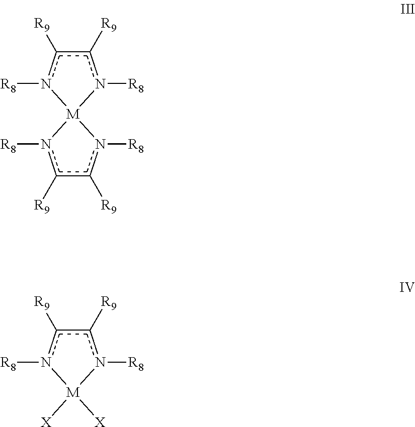
wherein:
M is a transition metal selected from groups 3-10 of the periodic table, Ru, Pd, Pt, Rh, Ir, Mg, Al, Sn, or Sb;
R8 is C1-C12 alkyl, amino (i.e., —NH2), or C6-C18 aryl;
R9 is hydrogen, C1-C10 alkyl, C6-C18 aryl, amino, C1-C12 alkylamino, or C2-C22 dialkylamino; and
X is Cl, Br, or I. The modified surface is then contacted with a vapor of an activating compound to form at least a portion of the thin film on the surface of the substrate. Characteristically, the activating compound is an acid or a diketone at a sufficient temperature to form a metal film.

wherein:
M is a transition metal selected from groups 3-10 of the periodic table, Ru, Pd, Pt, Rh, Ir, Mg, Al, Sn, or Sb;
R8 is C1-C12 alkyl, amino (i.e., —NH2), or C6-C18 aryl;
R9 is hydrogen, C1-C10 alkyl, C6-C18 aryl, amino, C1-C12 alkylamino, or C2-C22 dialkylamino; and
X is Cl, Br, or I. The first modified surface is then contacted with a vapor of an activating compound to form a second modified surface. Characteristically, the activating compound is an acid or a diketone. The second modified surface is then contacted with a reducing agent having formula IA or IB to form at least a portion of a metal film on the substrate.
-
- “ALD” is atomic layer deposition.
- “CVD is chemical vapor deposition.
- “RT” means “room temperature.”
- “s” means “seconds.”
- “THF” means “tetrahydrofuran.”
- “DME” means “1,2-dimethoxyethane.”
- “CHD” means 1,4-bis(trimethylsilyl)-2-methyl-1,4-cyclohexadiene.
- “DHP” means 1,4-bis(trimethylsilyl)-1,4-dihydropyrazine.
- “dmap” means “4-Dimethylaminopyridine.”
- “dad” means diazadiene.
- “dadtBu2” means “1,4-di-tert-butyldiazadiene.”
- “XPS” means “X-ray photoelectron spectroscopy.”
- “SEM” means “scanning electron microscopy.”
- “XRD” means “X-ray diffraction.”
- “acac” is acetylacetonate.
- “Cp” is cyclopentadienyl.
- “dmap” is 1-dimethylamino-2-methyl-2-propoxy.
- “en” is ethylene diamine.
- “Et” is ethyl.
- “EtCp” is ethylcyclopentadienyl.
- “Et2amd” is N,N′-diethylacetamidinate.
- “Et2fmd” is N,N′-diethylformamidinate.
- “hfac” is 1,1,1,5,5,5-hexafluoro-acetylacetonate.
- “iPr2amd” is N,N′-diisopropylacetamidinate.
- “iPr2fmd” is N,N′-diisopropylformamidinate.
- “iPrCp” is isopropylcyclopentadienyl.
- “Me” is methyl.
- “Me2amd” is N,N′-dimethylacetamidinate.
- “Me2fmd” is N,N′-dimethylformamidinate.
- “Mes” is 2,4,6-Me3C6H2 or mesityl.
- “MeCp” is methylcyclopentadienyl.
- “Me5 Cp” is pentamethylcyclopentadienyl.
- “Me2fmd” is N,N′-dimethylformamidinate.
- “Me2bmd” is N—N′-dimethylbutyramidinate.
- “Me2 pmd” is N,N′-dimethylpropionamidinate.
- “mmp” is 1-methoxy-2-methyl-2-propoxy.
- “OtPe” is tert-pentoxy.
- “od” is octane-2 4-dionate.
- “OiPr” is isopropoxy.
- “OtBu” is tert-butoxy.
- “OEt” is ethoxy.
- “tBu2amd” is N,N′-di-tert-butylacetamidinate.
- “tBuEtamd” is N-tert-butyl-N-ethylacetamidinate.
- “tBuEtpmd” is N-tert-butyl-N′-ethyl-propionamidinate.
- “tBuEtbmd” is N-tert-butyl-N′-ethylbutyramidinate.
- “thd” is 2,2,6,6-tetramethyl-heptane-3,5-dionate.
- “TEM” is transmission electron microscopy.
- “PXRD” is powder X-ray diffraction.
- “EDS” is Energy-dispersive X-ray spectroscopy.

wherein:
X1 is CR6(SiR1R1′R1″) or N(SiR1R1′R1″);
X2 is CR7(SiR1R1′R1″) or N(SiR1R1′R1″);
R1, R1′, R1″, R2, R3, R4, R5, R6, and R7 are each independently H, C1-10 alkyl, C6-14 aryl, or C4-14 heteroaryl.

and combinations thereof. The compound described by formula IIB is found to be particularly useful in forming metal-containing films. Particularly useful examples of the reducing agent are 1,4-bis(trimethylsilyl)-2-methyl-1,4-cyclohexadiene and 1,4-bis(trimethylsilyl)-1,4-dihydropyrazine.
MLn
MLnYm
wherein M is an atom selected from

with an activating compound. The activating compound is an acid or a diketone at a sufficient temperature to form a metal film,
wherein:
M is a transition metal selected from Groups 3-10 of the Periodic Table, Ru, Pd, Pt, Rh, and Ir;
In a refinement, M are the atoms in an oxidized state as set forth above;
R8 is C1-C12 alkyl, amino (i.e., —NH2), or C6-C18 aryl;
R9 is hydrogen, C1-C10 alkyl, C6-C18 aryl, amino, C1-C12 alkylamino, or C2-C22 dialkylamino and
X is Cl, Br, or I. In a refinement, M is Mg, Al, Ti, V, Cr, Mn, Fe, Co, Ni, Cu, Zn, Sn, or Sb. In another refinement, when the metal-containing compound has formula II, M is Cr, Mn, Fe, Ni, Co, Zn, Al, or Mg. In still another refinement, M is Mg, Al, Sn, or Sb. In a useful variation, the C2-5 diketone is a 1,3-diketone. It should be appreciated that the reaction of the present embodiment can be in the gas or liquid phases. In other variations, the reaction is an ALD reaction as set forth below.
M((NR10)2)n
wherein:
M is a metal selected from
R10 is C1-6 alkyl, Si(R11)3;
R11 is C1-6 alkyl, and
n is 2, 3, 4, 5, or 6.
M(OR10)n
wherein:
M is a metal selected from
R10 is C1-6 alkyl; and
n is 2, 3, 4, 5, or 6.

M is a metal selected from
R12, R13, R14 are independently H, C1-10 alkyl, C1-8 perfluoroalkyl, CF3, C1-10polyether groups, and the like; and
n is 2, 3, 4, 5, or 6.

wherein:
M is a metal selected from
R15, R16, R17 are independently H, C1-10 alkyl, C1-8 perfluoroalkyl, CF3, C1-10 polyether groups, and the like; and
n is 2, 3, 4, 5, or 6.

with an activating compound. The activating compound is an acid or a diketone at a sufficient temperature to form a metal film,
wherein:
M is a transition metal selected from Groups 3-10 of the Periodic Table, Ru, Pd, Pt, Rh, and Ir;
R8 is C1-C12 alkyl, amino (i.e., —NH2), or C6-C18 aryl;
R9 is hydrogen, C1-C10 alkyl, C6-C18 aryl, amino, C1-C12 alkylamino, or C2-C22 dialkylamino and
X is Cl, Br, or I. In a refinement, M is Mg, Al, Ti, V, Cr, Mn, Fe, Co, Ni, Cu, Zn, Sn, or Sb. In another refinement, when the metal-containing compound has formula II, M is Cr, Mn, Fe, Ni, Co, Zn, Al, or Mg. In still another refinement, M is Mg, Al, Sn, or Sb. In a useful variation, the C2-5 diketone is a 1,3-diketone. It should be appreciated that the reaction of the present embodiment can be in the gas or liquid phases. In other variations, the reaction is an ALD reaction as set forth below.
and a diazabutadiene ligand that is a dianion having the following formula:

| TABLE 1 |
| Solution reduction reactions of various metal salts with |
| 1,4-bis(trimethylsilyl)-2-methyl-1,4-cyclohexadiene. |
| Reaction |
| Reaction | Reflux | solution |
| Time | Time | → | |||||
| ML2 | Sol | Vol | Temp | (min) | Temp | (min) | Precipitate |
| CuCl2•H2O | THF | 15 | RT | 60 | — | — | milky white | |
| → CuCl | ||||||||
| (insoluble) | ||||||||
| CuCl2•H2O | THF | 50 |
0° C. | 5 | 65° C. | 65 | milky white | |
| → CuCl | ||||||||
| (insoluble) | ||||||||
| CuCl2•DME | DME | 45 | RT | 20 | 95° C. | 75 | milky white | |
| → add | ||||||||
| en → Cu | ||||||||
| metal | ||||||||
| CuBr2 | THF | 30 | RT | 60 | — | — | milky white | |
| → CuBr | ||||||||
| (probably) | ||||||||
| Cu(dmap)2 | |
15 | RT | 80 | 65° C. | 60 | dark orange | |
| → none | ||||||||
| Cu(hfac)2 | |
50 | RT | 35 | 65° C. | 60 | light green | |
| → none | ||||||||
| Cu(tmhd)2 | |
50 | RT | 60 | 65° C. | 60 | light | |
| blue → none | ||||||||
| Cu(HCOO)2 | |
50 |
0° C. | 5 | 65° C. | 60 | aqua green | |
| → none | ||||||||
| CoCl2 | THF | 50 | RT | 60 | 65° C. | 60 | light | |
| blue → none | ||||||||
| ZnCl2 | THF | 50 ml | RT | 105 | 65° C. | 60 | clear → | |
| none | ||||||||


| TABLE 2 |
| Representative values of the relative electronic energy |
| difference upon aromatization with respect to CHD. |
| ΔErel | |||||
| R2 | R3 | R4 | [kcal/mol] | ||
| H | H | H | −0.031 | ||
| CH3 | H | H | — | ||
| CH3 | CH3 | H | −3.038 | ||
| CH3 | H | CH3 | −0.036 | ||
| H | CH3 | CH3 | 0.089 | ||
| CH3 | CH3 | CH3 | −3.147 | ||
| NO2 | H | H | 1.346 | ||
| NO2 | NO2 | H | 0.585 | ||
| NO2 | H | NO2 | 4.162 | ||
| H | NO2 | NO2 | 4.982 | ||
| NO2 | NO2 | NO2 | 3.618 | ||
| OCH3 | H | H | 2.560 | ||
| OCH3 | OCH3 | H | −2.610 | ||
| OCH3 | H | OCH3 | 2.070 | ||
| H | OCH3 | OCH3 | 0.389 | ||
| OCH3 | OCH3 | OCH3 | −3.636 | ||
| Si(CH3)3 | H | H | −1.824 | ||
| CH3 | NO2 | H | 0.390 | ||
| CH3 | H | NO2 | 0.520 | ||
| H | CH3 | NO2 | 1.124 | ||
| CH3 | CH3 | NO2 | −2.737 | ||
| CH3 | NO2 | CH3 | 0.256 | ||
| NO2 | CH3 | CH3 | −1.648 | ||
| NO2 | NO2 | CH3 | 0.190 | ||
| NO2 | CH3 | NO2 | 2.487 | ||
| CH3 | NO2 | NO2 | 3.118 | ||

| TABLE 3 |
| Reaction matrix of metal salts with DHP |
| Reaction | Reflux |
| Time | Time | Reaction solution → | |||||
| ML2 | THF | Temp | (min) | Temp | (min) | Precipitate | |
| Cu(dmap)2 | 50 | RT | 15 | 65° C. | 60 | Cu flakes; Cu & | |
| green residue on | |||||||
| flask | |||||||
| Cu(tmhd)2 | 70 | RT | 30 | 65° C. | 95 | Cu & green flakes; | |
| Cu & purple residue | |||||||
| on | |||||||
| NiCl | |||||||
| 2 | 50 | RT | 15 | 65° C. | 70 | | |
| CoCl | |||||||
| 2 | 40 | RT | 35 | 65° C. | 60 | Dark green powder | |
| at RT (sticks to stir | |||||||
| bar) | |||||||
| FeCl2 | 60 | RT | 35 | 65° C. | 60 | Film on flask; black | |
| powder (sticks to | |||||||
| stir bar) | |||||||
| ZnCl2 | 75 | RT | 15 | 65° C. | 60 | Few metallic flakes | |
| → white precipitate | |||||||
| after about 3 | |||||||
| CrCl | |||||||
| 2 | 70 ml | RT | 23 | 65° C. | 60 | Silver-colored flakes | |
| → | |||||||
| MnCl | |||||||
| 2 | 50 | RT | 15 | 65° C. | 60 | None | |


Claims (30)
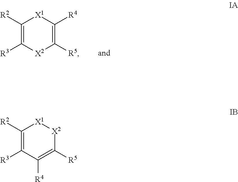


Priority Applications (2)
| Application Number | Priority Date | Filing Date | Title |
|---|---|---|---|
| US14/318,501 US9249505B2 (en) | 2013-06-28 | 2014-06-27 | Bis(trimethylsilyl) six-membered ring systems and related compounds as reducing agents for forming layers on a substrate |
| US15/010,762 US10533023B2 (en) | 2013-06-28 | 2016-01-29 | Bis(trimethylsilyl) six-membered ring systems and related compounds as reducing agents for forming layers on a substrate |
Applications Claiming Priority (4)
| Application Number | Priority Date | Filing Date | Title |
|---|---|---|---|
| US13/930,471 US9157149B2 (en) | 2013-06-28 | 2013-06-28 | Bis(trimethylsilyl) six-membered ring systems and related compounds as reducing agents for forming layers on a substrate |
| US201361902264P | 2013-11-10 | 2013-11-10 | |
| US201461974115P | 2014-04-02 | 2014-04-02 | |
| US14/318,501 US9249505B2 (en) | 2013-06-28 | 2014-06-27 | Bis(trimethylsilyl) six-membered ring systems and related compounds as reducing agents for forming layers on a substrate |
Related Parent Applications (1)
| Application Number | Title | Priority Date | Filing Date |
|---|---|---|---|
| US13/930,471 Continuation-In-Part US9157149B2 (en) | 2013-06-28 | 2013-06-28 | Bis(trimethylsilyl) six-membered ring systems and related compounds as reducing agents for forming layers on a substrate |
Related Child Applications (1)
| Application Number | Title | Priority Date | Filing Date |
|---|---|---|---|
| US15/010,762 Continuation US10533023B2 (en) | 2013-06-28 | 2016-01-29 | Bis(trimethylsilyl) six-membered ring systems and related compounds as reducing agents for forming layers on a substrate |
Publications (2)
| Publication Number | Publication Date |
|---|---|
| US20150004314A1 US20150004314A1 (en) | 2015-01-01 |
| US9249505B2 true US9249505B2 (en) | 2016-02-02 |
Family
ID=52115841
Family Applications (2)
| Application Number | Title | Priority Date | Filing Date |
|---|---|---|---|
| US14/318,501 Active US9249505B2 (en) | 2013-06-28 | 2014-06-27 | Bis(trimethylsilyl) six-membered ring systems and related compounds as reducing agents for forming layers on a substrate |
| US15/010,762 Active US10533023B2 (en) | 2013-06-28 | 2016-01-29 | Bis(trimethylsilyl) six-membered ring systems and related compounds as reducing agents for forming layers on a substrate |
Family Applications After (1)
| Application Number | Title | Priority Date | Filing Date |
|---|---|---|---|
| US15/010,762 Active US10533023B2 (en) | 2013-06-28 | 2016-01-29 | Bis(trimethylsilyl) six-membered ring systems and related compounds as reducing agents for forming layers on a substrate |
Country Status (1)
| Country | Link |
|---|---|
| US (2) | US9249505B2 (en) |
Cited By (2)
| Publication number | Priority date | Publication date | Assignee | Title |
|---|---|---|---|---|
| US10533023B2 (en) * | 2013-06-28 | 2020-01-14 | Wayne State University | Bis(trimethylsilyl) six-membered ring systems and related compounds as reducing agents for forming layers on a substrate |
| US11332486B2 (en) | 2018-12-26 | 2022-05-17 | Samsung Electronics Co., Ltd. | Aluminum compound and method for manufacturing semiconductor device using the same |
Families Citing this family (10)
| Publication number | Priority date | Publication date | Assignee | Title |
|---|---|---|---|---|
| TW201715070A (en) * | 2015-08-03 | 2017-05-01 | 韋恩州立大學 | 6-membered cyclic dienes as strongly reducing precursors for the growth of element films by vapor phase deposition |
| TWI770201B (en) | 2017-06-23 | 2022-07-11 | 德商馬克專利公司 | Methods of atomic layer deposition for selective film growth |
| CN111727272B (en) * | 2017-12-20 | 2023-04-28 | 巴斯夫欧洲公司 | Method for producing metal-containing films |
| US11421318B2 (en) * | 2018-05-04 | 2022-08-23 | Applied Materials, Inc. | Methods and apparatus for high reflectivity aluminum layers |
| TW202010746A (en) * | 2018-06-30 | 2020-03-16 | 美商應用材料股份有限公司 | TiN-containing precursors and methods of depositing tin-containing films |
| WO2020006379A1 (en) * | 2018-06-30 | 2020-01-02 | Applied Materials, Inc. | Deposition and etch processes of chromium-containing thin films for semiconductor manufacturing |
| KR102509744B1 (en) * | 2018-07-30 | 2023-03-15 | 주식회사 유피케미칼 | Aluminum compound and method for forming an aluminum-containing film using the same |
| TW202124757A (en) * | 2019-10-29 | 2021-07-01 | 美商應用材料股份有限公司 | Methods to grow low resistivity metal containing films |
| US11319449B2 (en) * | 2019-12-20 | 2022-05-03 | L'Air Liquide, Société Anonyme pour l'Etude et l'Exploitation des Procédés Georges Claude | Area selective deposition of metal containing films |
| US20220025514A1 (en) * | 2020-07-21 | 2022-01-27 | Wayne State University | Precursors And Processes For The Thermal ALD Of Cobalt Metal Thin Films |
Citations (22)
| Publication number | Priority date | Publication date | Assignee | Title |
|---|---|---|---|---|
| US3562308A (en) | 1967-07-25 | 1971-02-09 | Giacomo Costa | Process for producing organometallic chelated cobalt complexes |
| US5721014A (en) | 1995-12-19 | 1998-02-24 | Surface Tek Specialty Products, Inc. | Composition and method for reducing copper oxide to metallic copper |
| US6020511A (en) | 1996-10-02 | 2000-02-01 | Micron Technology, Inc. | Methods, complexes, and systems for forming metal-containing films |
| US20010009695A1 (en) | 2000-01-18 | 2001-07-26 | Saanila Ville Antero | Process for growing metalloid thin films |
| US20020013487A1 (en) | 2000-04-03 | 2002-01-31 | Norman John Anthony Thomas | Volatile precursors for deposition of metals and metal-containing films |
| US20020098346A1 (en) | 1998-03-27 | 2002-07-25 | Yissum Research Development Company Of The Hebrew University Of Jerusalem | Molecular layer epitaxy method and compositions |
| US6475276B1 (en) * | 1999-10-15 | 2002-11-05 | Asm Microchemistry Oy | Production of elemental thin films using a boron-containing reducing agent |
| US6786936B2 (en) | 1998-09-02 | 2004-09-07 | Micron Technology, Inc. | Methods, complexes, and systems for forming metal-containing films on semiconductor structures |
| US20050097991A1 (en) | 2003-09-19 | 2005-05-12 | Angel Sanjurjo | Methods and apparatuses for producing metallic compositions via reduction of metal halides |
| US20050186342A1 (en) | 2004-02-19 | 2005-08-25 | Nanosolar, Inc. | Formation of CIGS absorber layer materials using atomic layer deposition and high throughput surface treatment |
| US20060134331A1 (en) | 2004-08-16 | 2006-06-22 | Thompson Jeffery S | Atomic layer deposition of copper using surface-activation agents |
| US20060157863A1 (en) | 2005-01-19 | 2006-07-20 | Micron Technology, Inc. | Nucleation method for atomic layer deposition of cobalt on bare silicon during the formation of a semiconductor device |
| US20090114874A1 (en) | 2007-11-05 | 2009-05-07 | Air Products And Chemicals, Inc. | Copper Precursors for Thin Film Deposition |
| US7632351B2 (en) | 2005-08-08 | 2009-12-15 | E. I. Du Pont De Nemours And Company | Atomic layer deposition processes for the formation of ruthenium films, and ruthenium precursors useful in such processes |
| US20100104755A1 (en) | 2005-06-29 | 2010-04-29 | Christian Dussarrat | Deposition method of ternary films |
| KR20100061183A (en) | 2008-11-28 | 2010-06-07 | 주식회사 유피케미칼 | Organometallic precursors for deposition of metallic cobalt and cobalt containing ceramic films, and deposition process of the thin films |
| US20100181566A1 (en) | 2009-01-21 | 2010-07-22 | Synos Technology, Inc. | Electrode Structure, Device Comprising the Same and Method for Forming Electrode Structure |
| WO2012027357A2 (en) | 2010-08-24 | 2012-03-01 | Wayne State University | Thermally stable volatile precursors |
| US20120058270A1 (en) | 2009-05-15 | 2012-03-08 | Wayne State University | Thermally stable volatile film precursors |
| WO2012067439A2 (en) | 2010-11-17 | 2012-05-24 | 주식회사 유피케미칼 | Diazadiene-based metal compound, method for preparing same and method for forming a thin film using same |
| US20120231579A1 (en) | 2009-04-15 | 2012-09-13 | Micron Technology,Inc. | Methods Of Depositing Antimony-Comprising Phase Change Material Onto A Substrate And Methods Of Forming Phase Change Memory Circuitry |
| US20130115768A1 (en) | 2008-12-19 | 2013-05-09 | Viljami J. Pore | Methods for depositing nickel films and for making nickel silicide and nickel germanide |
Family Cites Families (14)
| Publication number | Priority date | Publication date | Assignee | Title |
|---|---|---|---|---|
| US3466270A (en) * | 1965-05-27 | 1969-09-09 | Gen Electric | Hydropyridines,triorganosilyl hydropyridines,and process for their preparation |
| US3781291A (en) * | 1971-05-26 | 1973-12-25 | R Sulzbach | Silylated 1,4-dihydropyridines |
| IL98174A0 (en) | 1991-05-17 | 1992-06-21 | Iscar Ltd | Chemical vapor deposition of diamond coatings on hard substrates |
| JP4112659B2 (en) | 1997-12-01 | 2008-07-02 | 大陽日酸株式会社 | Noble gas recovery method and apparatus |
| US7776394B2 (en) | 2005-08-08 | 2010-08-17 | E.I. Du Pont De Nemours And Company | Atomic layer deposition of metal-containing films using surface-activating agents |
| US7754906B2 (en) | 2005-10-07 | 2010-07-13 | Air Products And Chemicals, Inc. | Ti, Ta, Hf, Zr and related metal silicon amides for ALD/CVD of metal-silicon nitrides, oxides or oxynitrides |
| WO2007147020A2 (en) | 2006-06-15 | 2007-12-21 | Advanced Technology Materials, Inc. | Cobalt precursors useful for forming cobalt-containing films on substrates |
| JP2008031541A (en) | 2006-07-31 | 2008-02-14 | Tokyo Electron Ltd | Cvd film deposition process and cvd film deposition system |
| JP2011060910A (en) | 2009-09-08 | 2011-03-24 | Hitachi Kokusai Electric Inc | Substrate processing apparatus |
| US20120083134A1 (en) | 2010-09-30 | 2012-04-05 | Hui-Jung Wu | Method of mitigating substrate damage during deposition processes |
| WO2012176989A1 (en) | 2011-06-24 | 2012-12-27 | Up Chemical Co., Ltd. | A diamine compound or its salt, preparing method of the same, and uses of the same |
| JP2014534952A (en) | 2011-09-27 | 2014-12-25 | レール・リキード−ソシエテ・アノニム・プール・レテュード・エ・レクスプロワタシオン・デ・プロセデ・ジョルジュ・クロード | Tungsten diazabutadiene molecules, their synthesis and their use in the deposition of tungsten-containing films |
| US9157149B2 (en) * | 2013-06-28 | 2015-10-13 | Wayne State University | Bis(trimethylsilyl) six-membered ring systems and related compounds as reducing agents for forming layers on a substrate |
| US9249505B2 (en) * | 2013-06-28 | 2016-02-02 | Wayne State University | Bis(trimethylsilyl) six-membered ring systems and related compounds as reducing agents for forming layers on a substrate |
-
2014
- 2014-06-27 US US14/318,501 patent/US9249505B2/en active Active
-
2016
- 2016-01-29 US US15/010,762 patent/US10533023B2/en active Active
Patent Citations (23)
| Publication number | Priority date | Publication date | Assignee | Title |
|---|---|---|---|---|
| US3562308A (en) | 1967-07-25 | 1971-02-09 | Giacomo Costa | Process for producing organometallic chelated cobalt complexes |
| US5721014A (en) | 1995-12-19 | 1998-02-24 | Surface Tek Specialty Products, Inc. | Composition and method for reducing copper oxide to metallic copper |
| US6020511A (en) | 1996-10-02 | 2000-02-01 | Micron Technology, Inc. | Methods, complexes, and systems for forming metal-containing films |
| US20020098346A1 (en) | 1998-03-27 | 2002-07-25 | Yissum Research Development Company Of The Hebrew University Of Jerusalem | Molecular layer epitaxy method and compositions |
| US6786936B2 (en) | 1998-09-02 | 2004-09-07 | Micron Technology, Inc. | Methods, complexes, and systems for forming metal-containing films on semiconductor structures |
| US6475276B1 (en) * | 1999-10-15 | 2002-11-05 | Asm Microchemistry Oy | Production of elemental thin films using a boron-containing reducing agent |
| US20010009695A1 (en) | 2000-01-18 | 2001-07-26 | Saanila Ville Antero | Process for growing metalloid thin films |
| US20020013487A1 (en) | 2000-04-03 | 2002-01-31 | Norman John Anthony Thomas | Volatile precursors for deposition of metals and metal-containing films |
| US20050097991A1 (en) | 2003-09-19 | 2005-05-12 | Angel Sanjurjo | Methods and apparatuses for producing metallic compositions via reduction of metal halides |
| US20050186342A1 (en) | 2004-02-19 | 2005-08-25 | Nanosolar, Inc. | Formation of CIGS absorber layer materials using atomic layer deposition and high throughput surface treatment |
| US20060134331A1 (en) | 2004-08-16 | 2006-06-22 | Thompson Jeffery S | Atomic layer deposition of copper using surface-activation agents |
| US20060157863A1 (en) | 2005-01-19 | 2006-07-20 | Micron Technology, Inc. | Nucleation method for atomic layer deposition of cobalt on bare silicon during the formation of a semiconductor device |
| US20100104755A1 (en) | 2005-06-29 | 2010-04-29 | Christian Dussarrat | Deposition method of ternary films |
| US7632351B2 (en) | 2005-08-08 | 2009-12-15 | E. I. Du Pont De Nemours And Company | Atomic layer deposition processes for the formation of ruthenium films, and ruthenium precursors useful in such processes |
| US20090114874A1 (en) | 2007-11-05 | 2009-05-07 | Air Products And Chemicals, Inc. | Copper Precursors for Thin Film Deposition |
| KR20100061183A (en) | 2008-11-28 | 2010-06-07 | 주식회사 유피케미칼 | Organometallic precursors for deposition of metallic cobalt and cobalt containing ceramic films, and deposition process of the thin films |
| US20130115768A1 (en) | 2008-12-19 | 2013-05-09 | Viljami J. Pore | Methods for depositing nickel films and for making nickel silicide and nickel germanide |
| US20100181566A1 (en) | 2009-01-21 | 2010-07-22 | Synos Technology, Inc. | Electrode Structure, Device Comprising the Same and Method for Forming Electrode Structure |
| US20120231579A1 (en) | 2009-04-15 | 2012-09-13 | Micron Technology,Inc. | Methods Of Depositing Antimony-Comprising Phase Change Material Onto A Substrate And Methods Of Forming Phase Change Memory Circuitry |
| US20120058270A1 (en) | 2009-05-15 | 2012-03-08 | Wayne State University | Thermally stable volatile film precursors |
| WO2012027357A2 (en) | 2010-08-24 | 2012-03-01 | Wayne State University | Thermally stable volatile precursors |
| WO2012067439A2 (en) | 2010-11-17 | 2012-05-24 | 주식회사 유피케미칼 | Diazadiene-based metal compound, method for preparing same and method for forming a thin film using same |
| US20130251903A1 (en) | 2010-11-17 | 2013-09-26 | Up Chemical Co., Ltd. | Diazadiene-based metal compound, method for preparing same and method for forming a thin film using same |
Non-Patent Citations (61)
Cited By (2)
| Publication number | Priority date | Publication date | Assignee | Title |
|---|---|---|---|---|
| US10533023B2 (en) * | 2013-06-28 | 2020-01-14 | Wayne State University | Bis(trimethylsilyl) six-membered ring systems and related compounds as reducing agents for forming layers on a substrate |
| US11332486B2 (en) | 2018-12-26 | 2022-05-17 | Samsung Electronics Co., Ltd. | Aluminum compound and method for manufacturing semiconductor device using the same |
Also Published As
| Publication number | Publication date |
|---|---|
| US20150004314A1 (en) | 2015-01-01 |
| US20160289250A1 (en) | 2016-10-06 |
| US10533023B2 (en) | 2020-01-14 |
Similar Documents
| Publication | Publication Date | Title |
|---|---|---|
| US10533023B2 (en) | Bis(trimethylsilyl) six-membered ring systems and related compounds as reducing agents for forming layers on a substrate | |
| EP3013997B1 (en) | Bis(trimethylsilyl) six-membered ring systems and related compounds as reducing agents for forming layers on a substrate | |
| TWI630200B (en) | Volatile dihydropyrazinly and dihydropyrazine metal complexes | |
| US7371878B2 (en) | Tantalum amide complexes for depositing tantalum-containing films, and method of making same | |
| TWI427080B (en) | Deposition precursors for semiconductor applications | |
| US9157149B2 (en) | Bis(trimethylsilyl) six-membered ring systems and related compounds as reducing agents for forming layers on a substrate | |
| TWI570128B (en) | Nickel allyl amidinate precursors for deposition of nickel-containing films | |
| US20140179105A1 (en) | Heteroleptic (allyl)(pyrroles-2-aldiminate) metal-containing precursors, their synthesis and vapor deposition thereof to deposit metal-containing films | |
| EP3510038B1 (en) | Metal complexes containing allyl ligands | |
| JPWO2020071175A1 (en) | Raw materials for thin film formation for atomic layer deposition, raw materials for thin film formation, thin film manufacturing methods and compounds | |
| US10711346B2 (en) | 6-membered cyclic dienes as strongly reducing precursors for the growth of element films by vapor phase deposition | |
| US9790591B2 (en) | Titanium-containing film forming compositions for vapor deposition of titanium-containing films |
Legal Events
| Date | Code | Title | Description |
|---|---|---|---|
| AS | Assignment |
Owner name: WAYNE STATE UNIVERSITY, MICHIGAN Free format text: ASSIGNMENT OF ASSIGNORS INTEREST;ASSIGNORS:WINTER, CHARLES H.;KLESKO, JOSEPH PETER;REEL/FRAME:033343/0741 Effective date: 20140716 |
|
| STCF | Information on status: patent grant |
Free format text: PATENTED CASE |
|
| CC | Certificate of correction | ||
| MAFP | Maintenance fee payment |
Free format text: PAYMENT OF MAINTENANCE FEE, 4TH YR, SMALL ENTITY (ORIGINAL EVENT CODE: M2551); ENTITY STATUS OF PATENT OWNER: SMALL ENTITY Year of fee payment: 4 |
|
| MAFP | Maintenance fee payment |
Free format text: PAYMENT OF MAINTENANCE FEE, 8TH YR, SMALL ENTITY (ORIGINAL EVENT CODE: M2552); ENTITY STATUS OF PATENT OWNER: SMALL ENTITY Year of fee payment: 8 |