US9112352B2 - Condition responsive circuit protection apparatus which can enter an energy saving mode - Google Patents
Condition responsive circuit protection apparatus which can enter an energy saving mode Download PDFInfo
- Publication number
- US9112352B2 US9112352B2 US13/757,766 US201313757766A US9112352B2 US 9112352 B2 US9112352 B2 US 9112352B2 US 201313757766 A US201313757766 A US 201313757766A US 9112352 B2 US9112352 B2 US 9112352B2
- Authority
- US
- United States
- Prior art keywords
- terminal
- coupled
- power
- node
- circuit
- Prior art date
- Legal status (The legal status is an assumption and is not a legal conclusion. Google has not performed a legal analysis and makes no representation as to the accuracy of the status listed.)
- Expired - Fee Related, expires
Links
Images


Classifications
-
- H—ELECTRICITY
- H02—GENERATION; CONVERSION OR DISTRIBUTION OF ELECTRIC POWER
- H02H—EMERGENCY PROTECTIVE CIRCUIT ARRANGEMENTS
- H02H3/00—Emergency protective circuit arrangements for automatic disconnection directly responsive to an undesired change from normal electric working condition with or without subsequent reconnection ; integrated protection
- H02H3/08—Emergency protective circuit arrangements for automatic disconnection directly responsive to an undesired change from normal electric working condition with or without subsequent reconnection ; integrated protection responsive to excess current
- H02H3/087—Emergency protective circuit arrangements for automatic disconnection directly responsive to an undesired change from normal electric working condition with or without subsequent reconnection ; integrated protection responsive to excess current for dc applications
-
- H—ELECTRICITY
- H02—GENERATION; CONVERSION OR DISTRIBUTION OF ELECTRIC POWER
- H02J—CIRCUIT ARRANGEMENTS OR SYSTEMS FOR SUPPLYING OR DISTRIBUTING ELECTRIC POWER; SYSTEMS FOR STORING ELECTRIC ENERGY
- H02J7/00—Circuit arrangements for charging or depolarising batteries or for supplying loads from batteries
- H02J7/0029—Circuit arrangements for charging or depolarising batteries or for supplying loads from batteries with safety or protection devices or circuits
- H02J7/0036—Circuit arrangements for charging or depolarising batteries or for supplying loads from batteries with safety or protection devices or circuits using connection detecting circuits
-
- H—ELECTRICITY
- H02—GENERATION; CONVERSION OR DISTRIBUTION OF ELECTRIC POWER
- H02H—EMERGENCY PROTECTIVE CIRCUIT ARRANGEMENTS
- H02H3/00—Emergency protective circuit arrangements for automatic disconnection directly responsive to an undesired change from normal electric working condition with or without subsequent reconnection ; integrated protection
- H02H3/02—Details
- H02H3/04—Details with warning or supervision in addition to disconnection, e.g. for indicating that protective apparatus has functioned
Definitions
- the present invention relates to a circuit protection apparatus for detecting whether a peripheral component is plugged, damaged, or short-circuited; in particular, to a circuit protection apparatus which is able to automatically turn on or enter into a power saving mode, and is able to totally isolate the output power and the load automatically.
- the common electronic devices such as mobile phones, personal digital assistances (PDA), notebook computers, tablet computers, digital cameras, and digital camcorders, etc., are widely used by people, and become an indispensable part in the modern information life.
- FIG. 1 a shows a circuit block diagram of a short-circuit protection circuit used in universal serial bus (USB) port according to the conventional techniques.
- an output short-circuit protection is mainly based on the short-circuit protection by increasing or lowering the voltage within the integrated circuit (IC), and in the short-circuit protection of this kind of IC the time length of the short-circuit protection is usually set by connecting externally a RC circuit including resistors and capacitors. For example, when a short-circuit occurs, the time length when the power switch 103 stops outputting voltages and currents lies between a few tens of microseconds to a few seconds.
- the power converter 102 When the time at which the power switch 103 stops outputting both the voltages and currents is reached, the power converter 102 then will continuously output voltages and currents. If the short-circuit still exists, the short-circuit protection mentioned above is then executed again. Therefore, the output is opened and then closed for several times before the short-circuit problem is solved. This is due to the fact that the objective of the short-circuit protection of this kind of IC is for protecting the IC itself, and serves as the last protection stage when other external functions for protecting the circuits are inactivated. In other words, the short-circuit protection of this kind of IC cannot work when the product is short-circuited. Unfortunately, many electronic products are designed in this manner, which makes the safety of the short-circuit protection be seriously not enough, and is very easy to damage the external instruments or the inner circuits.
- this kind of IC does not have a current limitation protection, that is, when the external device generates abnormally large current because of current spike, aging, or interferences and the current is not large enough to cause a short circuit, it is still be deemed that the large current is normal and continuously outputted in this kind of IC, this situation is very easy to cause damages to the external devices.
- FIG. 1 b shows a circuit block diagram of a current limiting protection circuit of a USB port according to the conventional techniques.
- the circuit includes a USB port 104 , an amplifier 105 , a controller 106 , and a power converter 107 .
- the amplifier 105 outputs an enable signal EN.
- the controller 106 When the controller 106 receives the enable signal EN, the controller 106 leaves the power saving mode, which makes the power converter 107 to output fully electric energies.
- detection and enabling circuits are usually accompanied with a few power consumption, for example, even out of work, the amplifier 105 still has a basic power consumption. Those power consumptions usually may influence the usage time of the battery, and is easy to generate wrong operations.
- the disclosure discloses a circuit protection apparatus, which can automatically enter into a power saving mode or a power supply mode, and can automatically isolate totally the circuits between the output power and load when the circuit protection apparatus is short-circuited or the current exceeds a predetermined current. Then a warning component is actuated for warning the users.
- the disclosure discloses a power turn-on device, which uses a loop resistor without power consumption at normal time, the positive node (anode) of the terminals for outputting the power, and other two detection and turn-on switch components (such as a MOSFET or a bipolar transistor) for forming a cut-off loop.
- a close loop is formed for turning on or triggering the inner control circuits or other circuits, so as to achieve the objectives of the disclosure.
- the disclosure provides a circuit protection apparatus, for executing short-circuit protection to a peripheral interface.
- the peripheral interface includes a first power node and a second power node.
- the circuit protection apparatus includes a power converter, a power switch circuit, a warning circuit, and a controller.
- the power converter includes an input terminal and an output terminal.
- the input terminal of the power converter receives a control signal, and adjusts the voltage of the output terminal of the power converter according to the control signal.
- the power switch circuit includes an input terminal, an output terminal, a warning terminal, and an enable terminal.
- the input terminal of the power switch circuit is coupled to the output terminal of the power converter, and the output terminal of the power switch circuit is coupled to the first power node.
- the warning circuit includes a first terminal and a second terminal. The second terminal of the warning circuit is coupled to a common voltage.
- the controller includes a first control terminal, at least one warning control terminal, an enable control terminal, and an abnormity warning terminal.
- the first control terminal of the controller is coupled to the input terminal of the power converter, the warning control terminal of the controller is coupled to the first terminal of the warning circuit, the enable control terminal of the controller is coupled to the enable terminal of the power switch circuit, and the abnormity warning terminal of the controller is coupled to the warning terminal of the power switch circuit.
- the controller When a load is plugged to the peripheral interface and makes the first power node electrically connected with the second power node through the load, the controller is enabled and controls the power converter for outputting a power voltage, and the enable control terminal of the controller outputs an enable signal.
- the enable terminal of the power switch circuit receives the enable signal outputted by the controller, the input terminal and the output terminal of the power switch circuit turn on.
- the warning terminal of the power switch circuit When the load is too large and makes the first power node and the second power node short-circuited and thus the currents of the output terminal and the input terminal of the power switch circuit are larger than a predetermined current, then the warning terminal of the power switch circuit outputs an error flag logical voltage.
- the controller When the abnormity warning terminal of the controller receives the error flag logical voltage, the controller then turns off the power converter by using the first control terminal thereof, and turns off the power switch circuit by using the enable control terminal thereof, so that the input terminal and the output terminal of the power switch circuit are cut off. Moreover, the controller warns the users by conducting the warning circuit through the warning control terminal.
- the disclosure further provides a circuit protection method for executing short-circuit protection to a peripheral interface.
- the peripheral interface includes a first power node and a second power node.
- the short-circuit warning protection method includes: providing a power switch circuit between the first power node and a power converter, detecting the current magnitude between the input terminal and the output terminal of the power switch circuit; when the current between the input terminal and the output terminal of the power switch circuit is larger than a predetermined current, the power switch circuit outputs an error flag logical voltage; when the controller receives the error flag logical voltage, the current between the input terminal and the output terminal of the power switch circuit is cut off; stopping the operations of the power converter; and the warning component is actuated for noticing the users.
- the controller is enabled to output a control signal when the first switch is turned on, and the controller controls the second switch to turn on and uses the detection terminal for continuously detecting the voltage of the second power node.
- a switch circuit is added between the power converter and the power terminal of the peripheral interface, wherein the switch circuit has the functionalities for detecting the current or the voltage or both.
- the switch circuit may output a warning signal to notice a microprocessor, and the microprocessor may turn off the power converter immediately. Then the microprocessor can immediately conduct the warning components connected thereto, for making the users know that the plugged peripheral component is abnormal.
- the circuit protection apparatus in the disclosure can further enter into the power saving mode and the usage lifetime of the products is extended.
- FIG. 1 a shows a circuit block diagram of a short protection circuit applied to the USB port according to the conventional techniques
- FIG. 1 b shows a circuit block diagram of a current limiting protection circuit applied to the USB port according to the conventional techniques
- FIG. 2 shows a circuit block diagram of a circuit protection apparatus according to a first embodiment of the disclosure
- FIG. 3 shows a circuit block diagram of a circuit protection apparatus according to a second embodiment of the disclosure
- FIG. 4 shows a circuit block diagram of a circuit protection apparatus according to a third embodiment of the disclosure
- FIG. 5 shows a circuit block diagram of a circuit protection apparatus according to a fourth embodiment of the disclosure.
- FIG. 6 shows a circuit block diagram of a circuit protection apparatus according to a fifth embodiment of the disclosure.
- FIG. 7 shows a circuit block diagram of a circuit protection apparatus according to a sixth embodiment of the disclosure.
- FIG. 8 shows a circuit diagram of an output circuit for outputting error flags logical voltage within a circuit protection apparatus according to a seventh embodiment of the disclosure
- FIG. 9 shows a circuit diagram of an output circuit for outputting error flags logical voltage within a circuit protection apparatus according to an eighth embodiment of the disclosure.
- FIG. 10 shows a flow chart of a short circuit warning protection method according to the eighth embodiment of the disclosure.
- FIG. 2 shows a circuit block diagram of a circuit protection apparatus according to a first embodiment of the disclosure.
- the circuit protection apparatus includes an auxiliary power supply circuit 201 , a power converter 202 , a first switch 203 , a second switch 204 , and a controller 205 .
- the circuit protection apparatus provided by the disclosure is used for controlling a peripheral interface 206 .
- the peripheral interface 206 may be a DC jack, an earphone socket, a USB port, a mini USB, a micro USB, a military connection port, an industrial connection port, a medical connection port, a cosmetic connection port, or other connection ports.
- the embodiment does not limit the implementation type of the peripheral interface 206 .
- the peripheral interface 206 is, for example, a USB port.
- the peripheral interface 206 includes a first power node N 1 , a D ⁇ node N 2 , a D+ node N 3 , and a second power node N 4 .
- the auxiliary power supply circuit 201 includes a first terminal and a second terminal. The first terminal of the auxiliary power supply circuit 201 is coupled to a power voltage VCC, and the second terminal of the auxiliary power supply circuit 201 is coupled to the first power node N 1 .
- the power converter 202 includes an input terminal IN and an output terminal VOUT.
- the output terminal VOUT is coupled to the first power node N 1 .
- the input terminal IN receives a control signal, and adjusts the voltage of the output terminal VOUT of the power converter 202 .
- the first switch 203 includes a first terminal S 1 , a second terminal S 2 , and a control terminal SC.
- the second terminal S 2 of the first switch 203 is coupled to a common voltage
- the control terminal SC of the first switch 203 is coupled to the second power node N 4 .
- the common voltage in this embodiment is, for example, a ground.
- the second switch 204 includes a first terminal S 1 , a second terminal S 2 , and a control terminal SC.
- the second terminal S 2 of the second switch 204 is coupled to the common voltage, and the first terminal S 1 of the second switch 204 is coupled to the second power node N 4 .
- the controller 205 includes a first control terminal C 1 , a second control terminal C 2 , an enable terminal EN, and a detection terminal DT.
- the first terminal C 1 of the controller 205 is coupled to the input terminal IN of the power converter 202
- the second terminal C 2 of the controller 205 is coupled to the control terminal SC of the second switch 204
- the enable terminal EN of the controller 205 is coupled to the first terminal S 1 of the first switch 203
- the detection terminal DT of the controller 205 is coupled to the second power node N 4 .
- the first power node N 1 and the second power node N 4 are electrically connected with each other through the load L.
- the equivalent resistance of the load L is about 2.5 to 10 ohms and lets the power voltage VCC coupled by the auxiliary power supply circuit 201 be provided to the control terminal SC of the first switch 203 through the load L.
- the first terminal S 1 and the second terminal S 2 of the first switch 203 are conductive, and the enable terminal EN of the controller 205 receives the common voltage.
- the controller 205 is enabled, and the first control terminal C 1 of the controller 205 outputs a control signal for driving the output terminal VOUT of the power converter 202 to output power.
- the controller 205 controls the second switch 204 to turn on by using the second control terminal C 2 , and continuously detects the current or voltage of the second power node N 4 by using the detection terminal DT.
- both of the first control terminal C 1 and the second control terminal C 2 of the controller 205 stop outputting the control signals, and the controller 205 enters into the power saving mode.
- the predetermined voltage is such as 0.5V
- the controller 205 controls the power converter 202 to provide power.
- the controller 205 controls the power converter 202 to stop providing power.
- the present embodiment does not limit the value of the predetermined voltage.
- the auxiliary power supply circuit 201 cannot provide the power voltage VCC to the first switch 203 through the load L, thus the first switch 203 turns off.
- the detection terminal DT of the controller 205 detects that the current or voltage is lower than the predetermined value, the controller 205 than enters into the power saving mode, the power converter 202 is controlled to stop providing power, and the second switch 204 is also controlled to be turned off, thus the circuits recover to the status which does not consume power.
- the first switch 203 and the second switch 204 or some components will not consume electric power in a normal situation.
- the circuit loop is not formed, thus there is no loop current or other current. Therefore, the above embodiment of the disclosure can reduce the power consumptions under standby situation, and lengthen the usage lifetime of the products.
- the power converter 202 is, for example, a switching power converter including buck, boost, or buck-boost types.
- the disclosure does not limit the type of the power converter.
- the first switch 203 and the second switch 204 can be implemented by, for example, bipolar transistors or MOSFETs.
- FIG. 3 shows a circuit block diagram of a circuit protection apparatus according to a second embodiment of the disclosure.
- the circuit protection apparatus in this embodiment is applied to a peripheral interface 306 , such as a USB port or an IEEE 1394 etc.
- the peripheral interface 306 is, for example, a USB connection port interface which has four nodes including a first power node N 1 , a first data node N 2 , a second data node N 3 , and a second power node N 4 .
- the circuit protection apparatus includes a power converter 302 , a power switch circuit 307 , a warning circuit 309 , and a controller 305 .
- the power converter 302 includes an input terminal and an output terminal.
- the input terminal of the power converter 302 receives a control signal, and adjusts the voltage of the output terminal of the power converter 302 according to the control signal.
- the power converter 302 can be a switching power supply or a linear voltage regulator.
- the switching power supply can be divided into buck, boost, or flyback types, etc., according to the applications.
- the present embodiment does not limit the type of the power converter.
- the control signal may be a pulse width modulation (PWM) signal PWM.
- the power switch circuit 307 includes an input terminal IN, an output terminal OUT, a warning terminal ErrFlag, and an enable terminal EN.
- the input terminal IN of the power switch circuit 307 is coupled to the output terminal of the power converter 302
- the output terminal OUT of the power switch circuit 307 is coupled to the first power node N 1 .
- the warning circuit 309 includes a first terminal and a second terminal. The second terminal of the warning circuit 309 is coupled to a common voltage VCOM.
- the controller 305 includes a first control terminal C 1 , at least one warning control terminal L 1 , an enable control terminal ENC, and an abnormity warning terminal ERT.
- the first control terminal C 1 of the controller 305 is coupled to the input terminal of the power converter 302
- the warning control terminal L 1 of the controller 305 is coupled to the first terminal of the warning circuit 309
- the enable control terminal ENC of the controller 305 is coupled to the enable terminal EN of the power switch circuit 307
- the abnormity warning terminal ERT of the controller 305 is coupled to the warning terminal ErrFlag of the power switch circuit 307 .
- the peripheral component is plugged to the peripheral interface 306 and causes the first power node N 1 and the second power node N 4 to be electrically connected to each other through the load L.
- the controller 305 controls the power converter 302 to output a power voltage VCC, and the enable control terminal ENC of the controller 305 outputs an enable signal ES.
- the enable terminal EN of the power switch circuit 307 receives the enable signal ES, the input terminal IN and the output terminal OUT of the power switch circuit 307 are conductive. At this moment, the peripheral component can receive the power voltage VCC and stars to work.
- the warning terminal ErrFlag of the power switch circuit 307 outputs an error flag logical voltage ERR (such as a logical high voltage or a logical low voltage).
- the controller 305 When the abnormity warning terminal ERT of the controller 305 receives the error flag logical voltage ERR, the controller 305 turns off the power converter 302 by using the first control terminal C 1 , and turns off the power switch circuit 307 by using the enable control terminal ENC, so that the input terminal IN and the output terminal OUT of the power switch circuit 307 are cut off. In addition, the controller 305 turns on the warning circuit 309 by using the warning control terminal L 1 so as to notice the users. When the user sees the warning light or warning sounds emitted by the warning circuit 309 , the user can know that the plugged peripheral component may have some problems which cause a short circuit situation, thus the user may emergently remove the peripheral component for avoiding more damages.
- peripheral interface 306 coupled with one load L for illustration in this embodiment, however, in other embodiments, the disclosure can be used in a plurality of peripheral interfaces coupled to several loads.
- the circuit between the output power source and one of the loads in this disclosure can also be automatically and totally isolated, and the warning circuit is actuated for warning the users, while the original functions between the output power source and the rest of the loads are still be maintained.
- the circuits between the output power source and some of the loads in this disclosure can also be automatically and totally isolated, and the warning circuit is actuated for warning the users, while the original functions between the output power source and the rest of the loads are still be maintained.
- the present embodiment does not limit the type of the circuit protection apparatus.
- FIG. 4 shows a circuit block diagram of a circuit protection apparatus according to a third embodiment of the disclosure. Please refer to FIG. 4 , similarly, the circuit protection apparatus in this embodiment is applied to a peripheral interface 406 , such as a USB port interface or an IEEE 1394, etc. Supposing that the peripheral interface 406 here is a USB port interface which has four nodes, including a first power node N 1 , a first data node N 2 , a second data node N 3 , and a second power node N 4 .
- the circuit protection apparatus further includes a first switch 403 , a second switch 404 , and an auxiliary power supply circuit 401 .
- the warning circuit in this embodiment is illustrated by including some LEDs.
- the warning circuit can be, for example, a speaker including a buzzer or a loudspeaker, and the type of the warning circuit is not limited in this embodiment.
- the first switch 403 and the second switch 404 respectively include a first terminal S 1 , a second terminal S 2 , and a control terminal SC.
- the controller 405 further includes a second control terminal C 2 , an enable terminal EN, and a detection terminal DT.
- the second terminal C 2 of the controller 405 is coupled to the control terminal SC of the second switch 404
- the enable terminal EN of the controller 405 is coupled to the first terminal S 1 of the first switch 403
- the detection terminal DT of the controller 405 is coupled to the second power node N 4 .
- the peripheral component is plugged to the peripheral interface 406 and makes the first power node N 1 and the second power node N 4 be electrically connected through the load L.
- the equivalent resistance of the load L is about 2.5 to 10 ohms, so that the power voltage VCC coupled by the auxiliary power supply circuit 401 can be provided to the control terminal SC of the first switch 403 through the load L.
- the first terminal S 1 and the second terminal S 2 of the first switch 403 are conductive, and the enable terminal EN of the controller 405 receives the common voltage.
- the controller 405 After the enable terminal EN of the controller 405 receives the common voltage, the controller 405 is enabled, and the first control terminal C 1 of the controller 405 outputs the control signal for driving the output terminal of the power converter 402 so as to output power. After that, the controller 405 controls the second switch 404 to turn on by using the second control terminal C 2 , so as to form a circuit loop. Then, the controller 405 continuously detects the current or voltage of the second power node N 4 by using the detection terminal DT.
- the power switch circuit 407 When the load L is short-circuited or has too large current, the power switch circuit 407 generates an error flag logical voltage ERR to the controller 405 .
- the controller 405 then turns off the power switch circuit 407 by using the enable control terminal ENC, and simultaneously turns off the second switch 404 by using the second control terminal C 2 , so as to cut off the circuit loop between the first power node N 1 and the second power node N 4 of the peripheral interface 406 , and the controller 405 makes one or more LEDs (D 1 to D 5 ) to flicker simultaneously for warning the users.
- the mobile device usually has several light emitting circuits (usually LEDs) which are used for displaying the present power status or capacity of the batteries.
- the applicant may use the light emitting circuits as the warning circuit, for warning the users.
- the controller 405 detects that the current or voltage of the second power node N 4 is lower than a predetermined value, the first control terminal C 1 of the controller 405 then stops outputting the control signal, and the controller 405 controls the power converter 402 to stop outputting the power and enters into a power saving mode.
- the controller 405 detects that the current or voltage is lower than the predetermined value, the controller 405 enters into the power saving mode and controls the power converter 402 to stop outputting the power, and also controls the second switch 404 to turn off, so that the circuits recover to the status in which no electric power is consumed.
- the controller 405 controls the second switch 404 to turn on so as to form a circuit loop, thereby an enough voltage is provided to the control terminal SC of the first switch 403 .
- the controller 405 may continuously turn on the power switch circuit 407 and the second switch 404 , so that the power converter 402 can provide a power voltage to the load L.
- the controller 405 controls the power switch circuit 407 and the second switch 404 to turn off and turns on the warning circuit, thereby the efficacies of short-circuit warning protection is achieved.
- FIG. 5 shows a circuit block diagram of a circuit protection apparatus according to a fourth embodiment of the disclosure.
- the first switch and the second switch are implemented with MOSFETs.
- the circuit protection apparatus includes a first impedance component R 1 , a second impedance component R 2 , a third impedance component R 3 , a fourth impedance component R 4 , a power converter 502 , a first MOSFET M 1 , a second MOSFET M 2 , a power switch circuit 507 , and a controller 505 .
- the circuit protection apparatus provided in this embodiment is used for controlling a peripheral interface 506 .
- the peripheral interface 506 in this embodiment is, for example, a USB port, thus it is not repeatedly described.
- the operations of the controller 505 , the power switch circuit 507 , and the power converter 502 in this embodiment are similar to those in the first embodiment, thus they are not repeatedly described.
- the first impedance component R 1 is implemented by a resistor which includes a first terminal and a second terminal.
- the first terminal of the resistor is coupled to the second power node N 4 , and the second terminal of the resistor is coupled to the common voltage.
- the second impedance component R 2 is implemented by a resistor including a first terminal and a second terminal.
- the first terminal of the resistor is coupled to the second power node N 4
- the second terminal of the resistor is coupled to the first node of the second MOSFET M 2 .
- the third impedance component R 3 is implemented by a resistor including a first terminal and a second terminal.
- the first terminal of the resistor is coupled to the gate node of the second MOSFET M 2 , and the second terminal of the resistor is coupled to the common voltage.
- the auxiliary power supply circuit in this embodiment is implemented by, for example, the fourth impedance component R 4 .
- the fourth impedance component R 4 is a resistor and includes a first terminal and a second terminal. The first terminal of the resistor is coupled to a power voltage VCC, and the second terminal of the resistor is coupled to the first power node N 1 .
- the first MOSFET M 1 includes a gate node, a first node, and a second node.
- the gate node of the first MOSFET M 1 is coupled to the second power node N 4
- the first node of the first MOSFET M 1 is coupled to the enable terminal EN of the controller 505
- the second node of the first MOSFET M 1 is coupled to the common voltage.
- the second MOSFET M 2 includes a gate node, a first node, and a second node.
- the gate node of the second MOSFET M 2 is coupled to the second control terminal C 2 of the controller 505
- the first node of the second MOSFET M 2 is coupled to the second terminal of the second impedance component R 2
- the second node of the second MOSFET M 2 is coupled to the common voltage.
- the first MOSFET M 1 and the second MOSFET M 2 are used for implementing the first switch 403 and the second switch 404 .
- the MOSFETs M 1 and M 2 need bias voltages, the first impedance component R 1 , the second impedance component R 2 , the third impedance component R 3 , and the fourth impedance component R 4 are added additionally in this embodiment.
- the power voltage VCC may let the circuit between the first node and the second node of the first MOSFET M 1 be conductive by means of the voltage divided by the fourth impedance component R 4 and the first impedance component R 1 .
- the enable terminal EN of the controller 505 receives the common voltage and thus changes from the power saving mode to the turn-on mode. After the controller 505 enters into the turn-on mode, it may control the power converter 502 to begin to output the power voltage VCC. In addition, the controller 505 may control the second MOSFET M 2 to turn on.
- the detection terminal DT of the controller 505 is an input terminal of an analog to digital conversion, and the conversion is used for changing the voltage of the second power node N 4 into a digital value so that it is easier for the controller 505 to make determinations.
- RL represents the impedance of the load L.
- the above formula is obtained by ignoring the inner resistance of the second MOSFET M 2 . Because the impedance of RL is about 2.5 to 10 ohms, the USB peripheral components need about 5V ⁇ 5% for operation. For making the USB work normally, the value of the second impedance component R 2 cannot be selected to be too large.
- the voltage divided by the second impedance component R 2 and the impedance RL of the load L is about 0.1V, and the threshold is set to 0.05V.
- the load L is removed.
- the voltage of the second power node N 4 may discharge rapidly, thus the original 0.1V of the second power node N 4 starts to decrease.
- the controller 505 then enters into the power saving mode.
- the controller 505 controls the power converter 502 to stop outputting the power voltage VCC, controls the second MOSFET M 2 to turn off, and the controller 505 also controls itself to enter into the power saving mode.
- the power switch circuit 507 When the peripheral component is short-circuited, the instantaneous current between the input terminal IN and the output terminal OUT of the power switch circuit 507 will become too large, at this moment, the power switch circuit 507 outputs the error flag logical voltage ERR to the controller 505 .
- the controller 505 turns off the power switch circuit 507 by using the enable control terminal ENC, and simultaneously controls the second MOSFET M 2 to turn off by using the second control terminal C 2 , so as to cut off the circuit loop between the first power node N 1 and the second power node N 4 of the peripheral interface 506 .
- the controller 505 makes one or more LEDs D 1 to D 5 to flicker simultaneously for warning the users.
- FIG. 6 shows a circuit block diagram of a circuit protection apparatus according to a fifth embodiment of the disclosure.
- the first switch and the second switch in FIG. 5 are respectively implemented with the first MOSFET M 1 and the second MOSFET M 2 .
- the first switch and the second switch are respectively implemented with a first bipolar transistor Q 1 and a second bipolar transistor Q 2 .
- the first bipolar transistor Q 1 and the second bipolar transistor Q 2 are current driving components, thus more attention must be paid to the numeral design of the first impedance component R 1 and the fourth impedance component R 4 . Because, in addition to that the conducting voltage of the bipolar transistors Q 1 is 0.7V, the values of currents also need to be considered.
- portion of the operations in the fifth embodiment is equivalent to the counterpart in the third embodiment.
- the one skilled in the art can easily derive the operations in the fifth embodiment by referring to the third embodiment and the considered points above. Therefore, the operations are not repeatedly described.
- FIG. 7 shows a circuit block diagram of a circuit protection apparatus according to a sixth embodiment of the disclosure. Please refer to FIG. 7 along with FIG. 5 and FIG. 6 .
- the first switch is implemented with the bipolar transistor Q 1
- the second switch is implemented by the MOSFET M 2 . Because the operations are described in the third embodiment and the considered points and the selections of the resistance values are described in the fourth embodiment, the one skilled in the art may be able to change the implementations of the first and second switches between the bipolar transistors and the MOSFETs. Similarly, the one skilled in the art may also be able to implement the first switch with MOSFET while the second switch with the bipolar transistor.
- FIG. 8 shows a circuit diagram of the output circuit for outputting an error flag logical voltage within a circuit protection apparatus according to a seventh embodiment of the disclosure.
- the disclosure provides a mechanism for outputting the error flag logical voltage ERR.
- the circuit for outputting the error flag logical voltage includes a first resistor Z 1 , a second resistor Z 2 , a third resistor Z 3 , a fourth resistor Z 4 , a first amplifier A 1 , a second amplifier A 2 , and a third bipolar transistor Q 3 .
- the coupling relations thereof are shown in FIG. 8 .
- FIG. 9 shows a circuit diagram of the output circuit for outputting an error flag logical voltage within a circuit protection apparatus according to an eighth embodiment of the disclosure.
- the disclosure provides a mechanism for outputting the error flag logical voltage ERR.
- the circuit for outputting the error flag logical voltage includes a first resistor Z 1 , a second resistor Z 2 , a third resistor Z 3 , a fourth resistor Z 4 , and a first amplifier A 1 , and the coupling relations thereof are shown in FIG. 9 .
- the current flowing through the first resistor Z 1 is too large, and the voltages at the two terminals of the first amplifier A 1 are different, thus the first amplifier A 1 will output the error flag logical voltage ERR.
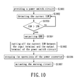
- FIG. 10 shows a flow chart for short-circuit warning protection method according to a ninth embodiment of the disclosure. Please refer to FIG. 10 , the method includes the following steps:
- Step S 1001 providing a power switch circuit between the first power node and the power converter.
- Step S 1002 detecting the value of the current ISW between the input terminal and the output terminal of the power switch circuit.
- Step S 1003 determining whether the current ISW between the input terminal and the output terminal of the power switch circuit is larger than a predetermined current IPR or not. If the current ISW is not larger than the current IPR, the method then goes back to the step S 1002 and continues execution. If the current ISW is larger than the current IPR, the step S 1004 is then executed.
- Step S 1004 when the current ISW between the input terminal and the output terminal of the power switch circuit is larger than the predetermined current IPR, the power switch circuit will output an error flag logical voltage ERR.
- Step S 1005 when the controller receives the error flag logical voltage ERR, the current ISW between the input terminal and the output terminal of the power switch circuit is cut off.
- Step S 1006 stopping the operations of the power converter.
- Step S 1007 actuating the warning circuit for noticing the users.
- the controller is enabled and output a control signal by turning on the first switch, so as to driving the power converter to output electric power.
- the controller controls the second switch to turn on, and continuously detects the voltage of the second power node by using the detection terminal.
- a power switch circuit is added between the power converter and the power node of the peripheral interface, and the power switch circuit has the function of detecting a voltage or a current or both.
- a warning signal is outputted for noticing a microprocessor, and the microprocessor may be able to turn off the power converter, and may immediately turn on the connected warning components, so as to let the user know that the plugged peripheral devices are abnormal.
- the controller in this disclosure can further enter immediately into the power saving mode for lengthening the usage lifetime of the products.
Landscapes
- Engineering & Computer Science (AREA)
- Power Engineering (AREA)
- Direct Current Feeding And Distribution (AREA)
- Protection Of Static Devices (AREA)
Abstract
Description
VN4=VCC×R2÷(R2+RL)
Claims (16)
Priority Applications (1)
| Application Number | Priority Date | Filing Date | Title |
|---|---|---|---|
| US13/757,766 US9112352B2 (en) | 2013-02-02 | 2013-02-02 | Condition responsive circuit protection apparatus which can enter an energy saving mode |
Applications Claiming Priority (1)
| Application Number | Priority Date | Filing Date | Title |
|---|---|---|---|
| US13/757,766 US9112352B2 (en) | 2013-02-02 | 2013-02-02 | Condition responsive circuit protection apparatus which can enter an energy saving mode |
Publications (2)
| Publication Number | Publication Date |
|---|---|
| US20140218200A1 US20140218200A1 (en) | 2014-08-07 |
| US9112352B2 true US9112352B2 (en) | 2015-08-18 |
Family
ID=51258789
Family Applications (1)
| Application Number | Title | Priority Date | Filing Date |
|---|---|---|---|
| US13/757,766 Expired - Fee Related US9112352B2 (en) | 2013-02-02 | 2013-02-02 | Condition responsive circuit protection apparatus which can enter an energy saving mode |
Country Status (1)
| Country | Link |
|---|---|
| US (1) | US9112352B2 (en) |
Cited By (1)
| Publication number | Priority date | Publication date | Assignee | Title |
|---|---|---|---|---|
| US20150289055A1 (en) * | 2014-04-08 | 2015-10-08 | Merry Electronics (Shenzhen) Co., Ltd. | Mobile device and corresponding noise-canceling earphone |
Families Citing this family (14)
| Publication number | Priority date | Publication date | Assignee | Title |
|---|---|---|---|---|
| US9702910B2 (en) * | 2013-08-26 | 2017-07-11 | Micropac Industries, Inc. | Power controller |
| US20150198670A1 (en) * | 2014-01-15 | 2015-07-16 | Laura Thiel | State-of-charge indicator |
| US10481211B2 (en) | 2014-01-15 | 2019-11-19 | Lat Enterprises, Inc. | State-of-charge indicator |
| WO2016037335A1 (en) * | 2014-09-11 | 2016-03-17 | Abb Technology Ltd | Protective circuit |
| US9871372B2 (en) * | 2014-10-07 | 2018-01-16 | Micropac Industries, Inc. | Voltage bus protection and isolation device |
| US20170358988A1 (en) * | 2014-12-17 | 2017-12-14 | Salcomp Oyj | Switched-mode power supply |
| CN105988962B (en) * | 2015-01-31 | 2018-10-12 | 鸿富锦精密工业(武汉)有限公司 | Overcurrent detecting system and circuit for detecting |
| CN106849028A (en) * | 2017-01-19 | 2017-06-13 | 珠海瑞捷电气股份有限公司 | A kind of on-load switch intelligent control unit |
| WO2018152993A1 (en) * | 2017-02-27 | 2018-08-30 | 华为技术有限公司 | Short-circuit fault handling apparatus and method |
| CN108370170B (en) * | 2017-02-27 | 2020-11-20 | 华为技术有限公司 | Short-circuit fault processing device and method |
| CN109783282B (en) * | 2017-11-15 | 2022-06-28 | 纬联电子科技(中山)有限公司 | Computer device and power supply abnormality detection method |
| US11176071B2 (en) | 2018-11-09 | 2021-11-16 | Cypress Semiconductor Corporation | USB signal switch circuitry using standard USB hub and method of operation the same |
| TWI693489B (en) * | 2019-06-24 | 2020-05-11 | 國立高雄科技大學 | Design method of DC ship micro-grid protection device |
| CN111766508A (en) * | 2020-07-21 | 2020-10-13 | 深圳宝龙达信创科技股份有限公司 | Short-circuit protection testing device |
Citations (1)
| Publication number | Priority date | Publication date | Assignee | Title |
|---|---|---|---|---|
| US20040218325A1 (en) * | 2003-04-29 | 2004-11-04 | Te-Fu Shih | Electronic power-saving power control circuit |
-
2013
- 2013-02-02 US US13/757,766 patent/US9112352B2/en not_active Expired - Fee Related
Patent Citations (1)
| Publication number | Priority date | Publication date | Assignee | Title |
|---|---|---|---|---|
| US20040218325A1 (en) * | 2003-04-29 | 2004-11-04 | Te-Fu Shih | Electronic power-saving power control circuit |
Cited By (2)
| Publication number | Priority date | Publication date | Assignee | Title |
|---|---|---|---|---|
| US20150289055A1 (en) * | 2014-04-08 | 2015-10-08 | Merry Electronics (Shenzhen) Co., Ltd. | Mobile device and corresponding noise-canceling earphone |
| US9338548B2 (en) * | 2014-04-08 | 2016-05-10 | Merry Electronics (Shenzhen) Co., Ltd. | Mobile device and corresponding noise-canceling earphone |
Also Published As
| Publication number | Publication date |
|---|---|
| US20140218200A1 (en) | 2014-08-07 |
Similar Documents
| Publication | Publication Date | Title |
|---|---|---|
| US9112352B2 (en) | Condition responsive circuit protection apparatus which can enter an energy saving mode | |
| US8947060B2 (en) | Regulator over-voltage protection circuit with reduced standby current | |
| US7719810B2 (en) | Overvoltage protection circuit and electronic device | |
| US9461455B2 (en) | Protecting circuit | |
| US9083181B2 (en) | Over-current protection circuit for light source driving module and related backlight module | |
| JP5708817B2 (en) | Load drive circuit | |
| US20150207307A1 (en) | Boost apparatus with over-current and over-voltage protection function | |
| KR101811741B1 (en) | An over-current protection circuit with foldback capability | |
| US20140085756A1 (en) | Protection circuit and electronic device using the same | |
| JP2010068637A (en) | Charge controlling semiconductor integrated circuit | |
| JP2013251518A (en) | Led drive circuit | |
| CN107342683B (en) | DCDC converter | |
| TWI548184B (en) | Protection device and method for electronic device | |
| US20120092800A1 (en) | Circuit for detecting over-voltage and over-current | |
| CN203251070U (en) | Circuit protection device | |
| KR101751547B1 (en) | Output circuit, temperature switch ic, and battery pack | |
| TW201507332A (en) | Boost apparatus with over-current and over-voltage protection function | |
| US20130119957A1 (en) | Bi-directional Switching Regulator and Control Circuit Thereof | |
| TWI479763B (en) | Protecion apparatus for a dc-dc converter | |
| TWI644495B (en) | Input protection circuit | |
| JP2014021634A (en) | Rush current suppression circuit | |
| TWI478457B (en) | Apparatus for circuit protection | |
| TWM459600U (en) | Apparatus for circuit protection | |
| JP2010220277A (en) | Abnormal voltage protection circuit | |
| JP4937085B2 (en) | Power supply with connector |
Legal Events
| Date | Code | Title | Description |
|---|---|---|---|
| AS | Assignment |
Owner name: CHEN, SHU-LING, TAIWAN Free format text: ASSIGNMENT OF ASSIGNORS INTEREST;ASSIGNOR:CHEN, SHU-LING;REEL/FRAME:029743/0797 Effective date: 20130131 Owner name: LIN, CHUN-FU, TAIWAN Free format text: ASSIGNMENT OF ASSIGNORS INTEREST;ASSIGNOR:CHEN, SHU-LING;REEL/FRAME:029743/0797 Effective date: 20130131 |
|
| STCF | Information on status: patent grant |
Free format text: PATENTED CASE |
|
| MAFP | Maintenance fee payment |
Free format text: PAYMENT OF MAINTENANCE FEE, 4TH YR, SMALL ENTITY (ORIGINAL EVENT CODE: M2551); ENTITY STATUS OF PATENT OWNER: SMALL ENTITY Year of fee payment: 4 |
|
| FEPP | Fee payment procedure |
Free format text: MAINTENANCE FEE REMINDER MAILED (ORIGINAL EVENT CODE: REM.); ENTITY STATUS OF PATENT OWNER: SMALL ENTITY |
|
| LAPS | Lapse for failure to pay maintenance fees |
Free format text: PATENT EXPIRED FOR FAILURE TO PAY MAINTENANCE FEES (ORIGINAL EVENT CODE: EXP.); ENTITY STATUS OF PATENT OWNER: SMALL ENTITY |
|
| STCH | Information on status: patent discontinuation |
Free format text: PATENT EXPIRED DUE TO NONPAYMENT OF MAINTENANCE FEES UNDER 37 CFR 1.362 |
|
| FP | Lapsed due to failure to pay maintenance fee |
Effective date: 20230818 |