US9110259B1 - Interleaved aliased AWG filter for continuous wideband wavelength discrimination - Google Patents
Interleaved aliased AWG filter for continuous wideband wavelength discrimination Download PDFInfo
- Publication number
- US9110259B1 US9110259B1 US14/616,488 US201514616488A US9110259B1 US 9110259 B1 US9110259 B1 US 9110259B1 US 201514616488 A US201514616488 A US 201514616488A US 9110259 B1 US9110259 B1 US 9110259B1
- Authority
- US
- United States
- Prior art keywords
- awg
- wavelength
- optical
- range
- response
- Prior art date
- Legal status (The legal status is an assumption and is not a legal conclusion. Google has not performed a legal analysis and makes no representation as to the accuracy of the status listed.)
- Active
Links
- 230000003287 optical effect Effects 0.000 claims abstract description 151
- 239000000835 fiber Substances 0.000 claims description 24
- 238000000034 method Methods 0.000 claims description 22
- 239000013307 optical fiber Substances 0.000 claims description 10
- 238000000926 separation method Methods 0.000 claims description 8
- 230000008878 coupling Effects 0.000 claims description 5
- 238000010168 coupling process Methods 0.000 claims description 5
- 238000005859 coupling reaction Methods 0.000 claims description 5
- 238000005259 measurement Methods 0.000 claims description 4
- 230000002457 bidirectional effect Effects 0.000 claims 1
- 239000000758 substrate Substances 0.000 description 8
- XUIMIQQOPSSXEZ-UHFFFAOYSA-N Silicon Chemical compound [Si] XUIMIQQOPSSXEZ-UHFFFAOYSA-N 0.000 description 6
- 230000005284 excitation Effects 0.000 description 6
- 239000010703 silicon Substances 0.000 description 6
- 229910052710 silicon Inorganic materials 0.000 description 6
- 238000004891 communication Methods 0.000 description 5
- 238000010586 diagram Methods 0.000 description 5
- VYPSYNLAJGMNEJ-UHFFFAOYSA-N Silicium dioxide Chemical compound O=[Si]=O VYPSYNLAJGMNEJ-UHFFFAOYSA-N 0.000 description 4
- 238000001228 spectrum Methods 0.000 description 4
- 238000005229 chemical vapour deposition Methods 0.000 description 3
- 238000005253 cladding Methods 0.000 description 3
- QVGXLLKOCUKJST-UHFFFAOYSA-N atomic oxygen Chemical compound [O] QVGXLLKOCUKJST-UHFFFAOYSA-N 0.000 description 2
- 238000013461 design Methods 0.000 description 2
- 229910052760 oxygen Inorganic materials 0.000 description 2
- 239000001301 oxygen Substances 0.000 description 2
- 239000000377 silicon dioxide Substances 0.000 description 2
- 238000013459 approach Methods 0.000 description 1
- 230000002238 attenuated effect Effects 0.000 description 1
- 230000005540 biological transmission Effects 0.000 description 1
- 229910052681 coesite Inorganic materials 0.000 description 1
- 238000010276 construction Methods 0.000 description 1
- 229910052906 cristobalite Inorganic materials 0.000 description 1
- 230000003247 decreasing effect Effects 0.000 description 1
- 230000000694 effects Effects 0.000 description 1
- 238000001914 filtration Methods 0.000 description 1
- 239000012212 insulator Substances 0.000 description 1
- 238000005468 ion implantation Methods 0.000 description 1
- 239000004973 liquid crystal related substance Substances 0.000 description 1
- 238000004519 manufacturing process Methods 0.000 description 1
- 238000013507 mapping Methods 0.000 description 1
- 239000003550 marker Substances 0.000 description 1
- 230000003647 oxidation Effects 0.000 description 1
- 238000007254 oxidation reaction Methods 0.000 description 1
- 238000001259 photo etching Methods 0.000 description 1
- 239000004038 photonic crystal Substances 0.000 description 1
- 238000012545 processing Methods 0.000 description 1
- 235000012239 silicon dioxide Nutrition 0.000 description 1
- 229910052682 stishovite Inorganic materials 0.000 description 1
- 229910052905 tridymite Inorganic materials 0.000 description 1
- 235000012431 wafers Nutrition 0.000 description 1
Images


Classifications
-
- G—PHYSICS
- G02—OPTICS
- G02B—OPTICAL ELEMENTS, SYSTEMS OR APPARATUS
- G02B6/00—Light guides; Structural details of arrangements comprising light guides and other optical elements, e.g. couplings
- G02B6/24—Coupling light guides
- G02B6/42—Coupling light guides with opto-electronic elements
- G02B6/4201—Packages, e.g. shape, construction, internal or external details
- G02B6/4204—Packages, e.g. shape, construction, internal or external details the coupling comprising intermediate optical elements, e.g. lenses, holograms
- G02B6/4215—Packages, e.g. shape, construction, internal or external details the coupling comprising intermediate optical elements, e.g. lenses, holograms the intermediate optical elements being wavelength selective optical elements, e.g. variable wavelength optical modules or wavelength lockers
-
- G—PHYSICS
- G01—MEASURING; TESTING
- G01D—MEASURING NOT SPECIALLY ADAPTED FOR A SPECIFIC VARIABLE; ARRANGEMENTS FOR MEASURING TWO OR MORE VARIABLES NOT COVERED IN A SINGLE OTHER SUBCLASS; TARIFF METERING APPARATUS; MEASURING OR TESTING NOT OTHERWISE PROVIDED FOR
- G01D5/00—Mechanical means for transferring the output of a sensing member; Means for converting the output of a sensing member to another variable where the form or nature of the sensing member does not constrain the means for converting; Transducers not specially adapted for a specific variable
- G01D5/26—Mechanical means for transferring the output of a sensing member; Means for converting the output of a sensing member to another variable where the form or nature of the sensing member does not constrain the means for converting; Transducers not specially adapted for a specific variable characterised by optical transfer means, i.e. using infrared, visible, or ultraviolet light
- G01D5/32—Mechanical means for transferring the output of a sensing member; Means for converting the output of a sensing member to another variable where the form or nature of the sensing member does not constrain the means for converting; Transducers not specially adapted for a specific variable characterised by optical transfer means, i.e. using infrared, visible, or ultraviolet light with attenuation or whole or partial obturation of beams of light
- G01D5/34—Mechanical means for transferring the output of a sensing member; Means for converting the output of a sensing member to another variable where the form or nature of the sensing member does not constrain the means for converting; Transducers not specially adapted for a specific variable characterised by optical transfer means, i.e. using infrared, visible, or ultraviolet light with attenuation or whole or partial obturation of beams of light the beams of light being detected by photocells
- G01D5/353—Mechanical means for transferring the output of a sensing member; Means for converting the output of a sensing member to another variable where the form or nature of the sensing member does not constrain the means for converting; Transducers not specially adapted for a specific variable characterised by optical transfer means, i.e. using infrared, visible, or ultraviolet light with attenuation or whole or partial obturation of beams of light the beams of light being detected by photocells influencing the transmission properties of an optical fibre
- G01D5/35306—Mechanical means for transferring the output of a sensing member; Means for converting the output of a sensing member to another variable where the form or nature of the sensing member does not constrain the means for converting; Transducers not specially adapted for a specific variable characterised by optical transfer means, i.e. using infrared, visible, or ultraviolet light with attenuation or whole or partial obturation of beams of light the beams of light being detected by photocells influencing the transmission properties of an optical fibre using an interferometer arrangement
- G01D5/35309—Mechanical means for transferring the output of a sensing member; Means for converting the output of a sensing member to another variable where the form or nature of the sensing member does not constrain the means for converting; Transducers not specially adapted for a specific variable characterised by optical transfer means, i.e. using infrared, visible, or ultraviolet light with attenuation or whole or partial obturation of beams of light the beams of light being detected by photocells influencing the transmission properties of an optical fibre using an interferometer arrangement using multiple waves interferometer
- G01D5/35316—Mechanical means for transferring the output of a sensing member; Means for converting the output of a sensing member to another variable where the form or nature of the sensing member does not constrain the means for converting; Transducers not specially adapted for a specific variable characterised by optical transfer means, i.e. using infrared, visible, or ultraviolet light with attenuation or whole or partial obturation of beams of light the beams of light being detected by photocells influencing the transmission properties of an optical fibre using an interferometer arrangement using multiple waves interferometer using a Bragg gratings
-
- G—PHYSICS
- G01—MEASURING; TESTING
- G01D—MEASURING NOT SPECIALLY ADAPTED FOR A SPECIFIC VARIABLE; ARRANGEMENTS FOR MEASURING TWO OR MORE VARIABLES NOT COVERED IN A SINGLE OTHER SUBCLASS; TARIFF METERING APPARATUS; MEASURING OR TESTING NOT OTHERWISE PROVIDED FOR
- G01D5/00—Mechanical means for transferring the output of a sensing member; Means for converting the output of a sensing member to another variable where the form or nature of the sensing member does not constrain the means for converting; Transducers not specially adapted for a specific variable
- G01D5/26—Mechanical means for transferring the output of a sensing member; Means for converting the output of a sensing member to another variable where the form or nature of the sensing member does not constrain the means for converting; Transducers not specially adapted for a specific variable characterised by optical transfer means, i.e. using infrared, visible, or ultraviolet light
- G01D5/32—Mechanical means for transferring the output of a sensing member; Means for converting the output of a sensing member to another variable where the form or nature of the sensing member does not constrain the means for converting; Transducers not specially adapted for a specific variable characterised by optical transfer means, i.e. using infrared, visible, or ultraviolet light with attenuation or whole or partial obturation of beams of light
- G01D5/34—Mechanical means for transferring the output of a sensing member; Means for converting the output of a sensing member to another variable where the form or nature of the sensing member does not constrain the means for converting; Transducers not specially adapted for a specific variable characterised by optical transfer means, i.e. using infrared, visible, or ultraviolet light with attenuation or whole or partial obturation of beams of light the beams of light being detected by photocells
- G01D5/353—Mechanical means for transferring the output of a sensing member; Means for converting the output of a sensing member to another variable where the form or nature of the sensing member does not constrain the means for converting; Transducers not specially adapted for a specific variable characterised by optical transfer means, i.e. using infrared, visible, or ultraviolet light with attenuation or whole or partial obturation of beams of light the beams of light being detected by photocells influencing the transmission properties of an optical fibre
- G01D5/35383—Mechanical means for transferring the output of a sensing member; Means for converting the output of a sensing member to another variable where the form or nature of the sensing member does not constrain the means for converting; Transducers not specially adapted for a specific variable characterised by optical transfer means, i.e. using infrared, visible, or ultraviolet light with attenuation or whole or partial obturation of beams of light the beams of light being detected by photocells influencing the transmission properties of an optical fibre using multiple sensor devices using multiplexing techniques
- G01D5/35387—Mechanical means for transferring the output of a sensing member; Means for converting the output of a sensing member to another variable where the form or nature of the sensing member does not constrain the means for converting; Transducers not specially adapted for a specific variable characterised by optical transfer means, i.e. using infrared, visible, or ultraviolet light with attenuation or whole or partial obturation of beams of light the beams of light being detected by photocells influencing the transmission properties of an optical fibre using multiple sensor devices using multiplexing techniques using wavelength division multiplexing
-
- G—PHYSICS
- G01—MEASURING; TESTING
- G01J—MEASUREMENT OF INTENSITY, VELOCITY, SPECTRAL CONTENT, POLARISATION, PHASE OR PULSE CHARACTERISTICS OF INFRARED, VISIBLE OR ULTRAVIOLET LIGHT; COLORIMETRY; RADIATION PYROMETRY
- G01J3/00—Spectrometry; Spectrophotometry; Monochromators; Measuring colours
- G01J3/02—Details
- G01J3/0205—Optical elements not provided otherwise, e.g. optical manifolds, diffusers, windows
- G01J3/0218—Optical elements not provided otherwise, e.g. optical manifolds, diffusers, windows using optical fibers
-
- G—PHYSICS
- G01—MEASURING; TESTING
- G01J—MEASUREMENT OF INTENSITY, VELOCITY, SPECTRAL CONTENT, POLARISATION, PHASE OR PULSE CHARACTERISTICS OF INFRARED, VISIBLE OR ULTRAVIOLET LIGHT; COLORIMETRY; RADIATION PYROMETRY
- G01J3/00—Spectrometry; Spectrophotometry; Monochromators; Measuring colours
- G01J3/12—Generating the spectrum; Monochromators
- G01J3/18—Generating the spectrum; Monochromators using diffraction elements, e.g. grating
- G01J3/1895—Generating the spectrum; Monochromators using diffraction elements, e.g. grating using fiber Bragg gratings or gratings integrated in a waveguide
-
- G—PHYSICS
- G01—MEASURING; TESTING
- G01J—MEASUREMENT OF INTENSITY, VELOCITY, SPECTRAL CONTENT, POLARISATION, PHASE OR PULSE CHARACTERISTICS OF INFRARED, VISIBLE OR ULTRAVIOLET LIGHT; COLORIMETRY; RADIATION PYROMETRY
- G01J3/00—Spectrometry; Spectrophotometry; Monochromators; Measuring colours
- G01J3/28—Investigating the spectrum
- G01J3/30—Measuring the intensity of spectral lines directly on the spectrum itself
- G01J3/36—Investigating two or more bands of a spectrum by separate detectors
-
- G—PHYSICS
- G02—OPTICS
- G02B—OPTICAL ELEMENTS, SYSTEMS OR APPARATUS
- G02B6/00—Light guides; Structural details of arrangements comprising light guides and other optical elements, e.g. couplings
- G02B6/24—Coupling light guides
- G02B6/26—Optical coupling means
- G02B6/28—Optical coupling means having data bus means, i.e. plural waveguides interconnected and providing an inherently bidirectional system by mixing and splitting signals
- G02B6/293—Optical coupling means having data bus means, i.e. plural waveguides interconnected and providing an inherently bidirectional system by mixing and splitting signals with wavelength selective means
- G02B6/29304—Optical coupling means having data bus means, i.e. plural waveguides interconnected and providing an inherently bidirectional system by mixing and splitting signals with wavelength selective means operating by diffraction, e.g. grating
-
- G—PHYSICS
- G02—OPTICS
- G02B—OPTICAL ELEMENTS, SYSTEMS OR APPARATUS
- G02B6/00—Light guides; Structural details of arrangements comprising light guides and other optical elements, e.g. couplings
- G02B6/24—Coupling light guides
- G02B6/26—Optical coupling means
- G02B6/28—Optical coupling means having data bus means, i.e. plural waveguides interconnected and providing an inherently bidirectional system by mixing and splitting signals
- G02B6/293—Optical coupling means having data bus means, i.e. plural waveguides interconnected and providing an inherently bidirectional system by mixing and splitting signals with wavelength selective means
- G02B6/29379—Optical coupling means having data bus means, i.e. plural waveguides interconnected and providing an inherently bidirectional system by mixing and splitting signals with wavelength selective means characterised by the function or use of the complete device
- G02B6/2938—Optical coupling means having data bus means, i.e. plural waveguides interconnected and providing an inherently bidirectional system by mixing and splitting signals with wavelength selective means characterised by the function or use of the complete device for multiplexing or demultiplexing, i.e. combining or separating wavelengths, e.g. 1xN, NxM
-
- G—PHYSICS
- G02—OPTICS
- G02B—OPTICAL ELEMENTS, SYSTEMS OR APPARATUS
- G02B6/00—Light guides; Structural details of arrangements comprising light guides and other optical elements, e.g. couplings
- G02B6/24—Coupling light guides
- G02B6/26—Optical coupling means
- G02B6/34—Optical coupling means utilising prism or grating
-
- G—PHYSICS
- G02—OPTICS
- G02B—OPTICAL ELEMENTS, SYSTEMS OR APPARATUS
- G02B6/00—Light guides; Structural details of arrangements comprising light guides and other optical elements, e.g. couplings
- G02B6/24—Coupling light guides
- G02B6/42—Coupling light guides with opto-electronic elements
- G02B6/4298—Coupling light guides with opto-electronic elements coupling with non-coherent light sources and/or radiation detectors, e.g. lamps, incandescent bulbs, scintillation chambers
-
- H—ELECTRICITY
- H04—ELECTRIC COMMUNICATION TECHNIQUE
- H04J—MULTIPLEX COMMUNICATION
- H04J14/00—Optical multiplex systems
- H04J14/02—Wavelength-division multiplex systems
-
- G—PHYSICS
- G02—OPTICS
- G02B—OPTICAL ELEMENTS, SYSTEMS OR APPARATUS
- G02B6/00—Light guides; Structural details of arrangements comprising light guides and other optical elements, e.g. couplings
- G02B6/02—Optical fibres with cladding with or without a coating
- G02B6/02057—Optical fibres with cladding with or without a coating comprising gratings
- G02B6/02076—Refractive index modulation gratings, e.g. Bragg gratings
- G02B6/0208—Refractive index modulation gratings, e.g. Bragg gratings characterised by their structure, wavelength response
- G02B6/02085—Refractive index modulation gratings, e.g. Bragg gratings characterised by their structure, wavelength response characterised by the grating profile, e.g. chirped, apodised, tilted, helical
-
- G—PHYSICS
- G02—OPTICS
- G02B—OPTICAL ELEMENTS, SYSTEMS OR APPARATUS
- G02B6/00—Light guides; Structural details of arrangements comprising light guides and other optical elements, e.g. couplings
- G02B6/02—Optical fibres with cladding with or without a coating
- G02B6/02057—Optical fibres with cladding with or without a coating comprising gratings
- G02B6/02076—Refractive index modulation gratings, e.g. Bragg gratings
- G02B6/02123—Refractive index modulation gratings, e.g. Bragg gratings characterised by the method of manufacture of the grating
- G02B6/02133—Refractive index modulation gratings, e.g. Bragg gratings characterised by the method of manufacture of the grating using beam interference
- G02B6/02138—Refractive index modulation gratings, e.g. Bragg gratings characterised by the method of manufacture of the grating using beam interference based on illuminating a phase mask
-
- G—PHYSICS
- G02—OPTICS
- G02B—OPTICAL ELEMENTS, SYSTEMS OR APPARATUS
- G02B6/00—Light guides; Structural details of arrangements comprising light guides and other optical elements, e.g. couplings
- G02B6/02—Optical fibres with cladding with or without a coating
- G02B6/02057—Optical fibres with cladding with or without a coating comprising gratings
- G02B6/02076—Refractive index modulation gratings, e.g. Bragg gratings
- G02B6/02195—Refractive index modulation gratings, e.g. Bragg gratings characterised by means for tuning the grating
- G02B6/022—Refractive index modulation gratings, e.g. Bragg gratings characterised by means for tuning the grating using mechanical stress, e.g. tuning by compression or elongation, special geometrical shapes such as "dog-bone" or taper
-
- G—PHYSICS
- G02—OPTICS
- G02B—OPTICAL ELEMENTS, SYSTEMS OR APPARATUS
- G02B6/00—Light guides; Structural details of arrangements comprising light guides and other optical elements, e.g. couplings
- G02B6/10—Light guides; Structural details of arrangements comprising light guides and other optical elements, e.g. couplings of the optical waveguide type
- G02B6/12—Light guides; Structural details of arrangements comprising light guides and other optical elements, e.g. couplings of the optical waveguide type of the integrated circuit kind
- G02B6/12007—Light guides; Structural details of arrangements comprising light guides and other optical elements, e.g. couplings of the optical waveguide type of the integrated circuit kind forming wavelength selective elements, e.g. multiplexer, demultiplexer
-
- G—PHYSICS
- G02—OPTICS
- G02B—OPTICAL ELEMENTS, SYSTEMS OR APPARATUS
- G02B6/00—Light guides; Structural details of arrangements comprising light guides and other optical elements, e.g. couplings
- G02B6/10—Light guides; Structural details of arrangements comprising light guides and other optical elements, e.g. couplings of the optical waveguide type
- G02B6/12—Light guides; Structural details of arrangements comprising light guides and other optical elements, e.g. couplings of the optical waveguide type of the integrated circuit kind
- G02B6/122—Basic optical elements, e.g. light-guiding paths
- G02B6/124—Geodesic lenses or integrated gratings
-
- G—PHYSICS
- G02—OPTICS
- G02B—OPTICAL ELEMENTS, SYSTEMS OR APPARATUS
- G02B6/00—Light guides; Structural details of arrangements comprising light guides and other optical elements, e.g. couplings
- G02B6/24—Coupling light guides
- G02B6/26—Optical coupling means
- G02B6/28—Optical coupling means having data bus means, i.e. plural waveguides interconnected and providing an inherently bidirectional system by mixing and splitting signals
- G02B6/293—Optical coupling means having data bus means, i.e. plural waveguides interconnected and providing an inherently bidirectional system by mixing and splitting signals with wavelength selective means
- G02B6/29379—Optical coupling means having data bus means, i.e. plural waveguides interconnected and providing an inherently bidirectional system by mixing and splitting signals with wavelength selective means characterised by the function or use of the complete device
- G02B6/2938—Optical coupling means having data bus means, i.e. plural waveguides interconnected and providing an inherently bidirectional system by mixing and splitting signals with wavelength selective means characterised by the function or use of the complete device for multiplexing or demultiplexing, i.e. combining or separating wavelengths, e.g. 1xN, NxM
- G02B6/29382—Optical coupling means having data bus means, i.e. plural waveguides interconnected and providing an inherently bidirectional system by mixing and splitting signals with wavelength selective means characterised by the function or use of the complete device for multiplexing or demultiplexing, i.e. combining or separating wavelengths, e.g. 1xN, NxM including at least adding or dropping a signal, i.e. passing the majority of signals
- G02B6/29383—Adding and dropping
-
- G—PHYSICS
- G02—OPTICS
- G02B—OPTICAL ELEMENTS, SYSTEMS OR APPARATUS
- G02B6/00—Light guides; Structural details of arrangements comprising light guides and other optical elements, e.g. couplings
- G02B6/24—Coupling light guides
- G02B6/26—Optical coupling means
- G02B6/28—Optical coupling means having data bus means, i.e. plural waveguides interconnected and providing an inherently bidirectional system by mixing and splitting signals
- G02B6/293—Optical coupling means having data bus means, i.e. plural waveguides interconnected and providing an inherently bidirectional system by mixing and splitting signals with wavelength selective means
- G02B6/29379—Optical coupling means having data bus means, i.e. plural waveguides interconnected and providing an inherently bidirectional system by mixing and splitting signals with wavelength selective means characterised by the function or use of the complete device
- G02B6/29395—Optical coupling means having data bus means, i.e. plural waveguides interconnected and providing an inherently bidirectional system by mixing and splitting signals with wavelength selective means characterised by the function or use of the complete device configurable, e.g. tunable or reconfigurable
Definitions
- the present invention relates to arrayed waveguide (AWG) filters for resolution of a wavelength presented to a wavelength discriminator.
- AWG arrayed waveguide
- the present invention relates to the use of AWG filters with aliasing responses for use in discrimination of wavelengths at aliasing responses of the AWG filter.
- a wavelength interrogator typically uses a sine filter or other type of wavelength sensitive filter which has a monotonic response to a shift in incoming wavelength, with the wavelength interrogator coupled to a fiber Bragg grating (FBG) sensor, which may be place in series with other FBG sensors, each sensor having a corresponding wavelength discriminator.
- FBG fiber Bragg grating
- sine filters are individual components, each of which is tuned to operate in a particular range of wavelengths. It is desired to provide a wavelength interrogator architecture where the number of sensors which may be deployed is not limited by the number of discrete sine filters or other filters which resolve wavelength into detector response in the interrogator.
- a first object of the invention is an optical interrogator which uses an arrayed waveguide grating to perform wavelength discrimination.
- a second object of the invention is a wavelength interrogator having a broadband source coupled to a circulator, the circulator transferring optical energy from the broadband source to a sensing optical fiber having a plurality of fiber gratings for sensing, each fiber grating operating in a unique wavelength range, reflected optical energy from the fiber gratings reflected back to the circulator, the circulator directing the energy to an AWG input port, each fiber grating returning optical energy in a skirt response region of a unique channel of the AWG, a unique channel of the AWG coupled to a detector, the adjacent detector responses of each AWG channel used to determine the response wavelength of an associated fiber sensor.
- a third object of the invention is a wavelength interrogator having a plurality of broadband sources, each broadband source operative in a particular and unique wavelength range associated with a particular sensor string, the broadband sources coupled to a circulator which couples the optical energy from the broadband sources to a plurality of fiber sensor strings, each fiber sensor string having a plurality of fiber Bragg gratings responsive to wavelengths of one of the broadband sources, each fiber sensor string grating also generating a unique wavelength reflection for each sensor, the optical energy from the sensors returned through the circulator to an AWG having a plurality of channels, each channel coupled to a detector, the detectors of adjacent channels of the AWG used to determine the wavelength of a particular sensor in each particular broadband source response range.
- a fourth object of the invention is an aliasing AWG interrogator which utilizes a first AWG filter with a response in a first wavelength range which is adjacent to the wavelength range of a second AWG filter, where the lowest wavelength of the first AWG aliases to a wavelength greater than the highest wavelength of the second AWG filter.
- a fifth object of the invention is an aliasing AWG interrogator which utilizes a first AWG filter with a response in a first wavelength range and a second AWG filter with a response in a second wavelength range, the first AWG filter wavelength range adjacent to the second AWG filter wavelength range, where the lowest wavelength of the first AWG range also aliases to a wavelength adjacent to the highest wavelength of the second AWG filter, the aliasing AWG interrogator thereby able to discriminate wavelength when coupled to a string of fiber Bragg gratings (FBGs), each FBG responsive in a unique range of wavelengths corresponding to a fundamental response range of two adjacent AWG filters or the alias response of the two adjacent AWG filters, the string of FBGs excited by an optical source having a bandwidth equal or less than the sum of the first AWG filter wavelength range and second AWG filter wavelength range.
- FBGs fiber Bragg gratings
- An optical fiber with a plurality of sequential gratings is coupled to a circulator or directional coupler, such that the circulator or directional coupler receives broadband optical energy from the broadband source and couples the broadband optical energy to an optical fiber with the plurality of gratings operative as sensors having gratings.
- Reflected energy from the plurality of sequential gratings is directed through the circulator to the input of an array waveguide grating (AWG), which segregates each wavelength to a particular AWG output channel.
- AWG grating responses and AWG response skirts are selected such that the grating response occurs in an AWG response skirt, and each channel of the AWG is coupled to an associated detector. Detectors for adjacent channels are measured for a response, and the combined response of two adjacent channels is used to determine the reflected wavelength for a particular sensor to perform wavelength interrogation which converts the measured detector output to the corresponding wavelength.
- each sensor string responsive to one of a plurality of selectable sources, and each sensor of each string is operative in a unique wavelength range and used with an AWG which generates a wavelength aliasing (repeating) response
- a single AWG can be used, with each sensor string receiving excitation from a separate broadband source operative in the wavelength range of that particular sensor string.
- the present invention thereby provides simultaneous interrogation of a plurality n/2 of sensors using adjacent AWG channel detector responses in an AWG having n channels.
- FIG. 1 is a block diagram of two AWG filters used in a communication link.
- FIG. 2 is a plot of the wavelength response of the filter of FIG. 1 .
- FIG. 3 is a schematic view of an AWG filter.
- FIG. 4 is a diffraction optics equivalent to the AWG filter of FIG. 3 .
- FIG. 5 is a wavelength interrogator for use with a plurality of gratings located on a single optical fiber.
- FIG. 6 is a wavelength discrimination plot for the interrogator of FIG. 5 and FIG. 9 .
- FIG. 7 is an AWG response plot for adjacent channels.
- FIG. 8 is a plot of adjacent channel detector responses.
- FIG. 9 is a block diagram for an interrogator using a single AWG with an aliasing response, and interrogating a plurality of sensor strings, each string operative in its own wavelength band, but using the same AWG for wavelength discrimination.
- FIG. 10 is a block diagram for a 2-way AWG filter used in a wavelength interrogator.
- FIG. 11A is a simplified response plot of the AWG filters of FIG. 10 .
- FIG. 11B is a response plot of the AWG filters of FIG. 11A showing the individual AWG channel responses.
- FIGS. 11C and 11D show detail plots of AWG filter response.
- FIG. 12 is a block diagram of a 2-way AWG filter used with CWDM filters.
- FIG. 13 is a plot of a non-overlapping AWG filter showing ranges of operation.
- FIG. 14 is a plot of the wavelength responses of a second AWG filter offset from a first AWG filter of FIG. 13 .
- AWG filters are widely used in telecommunications to provide unique wavelength response in a WDM (wavelength division multiplexing) system which assigns adjacent wavelengths to independent communication sessions, and the AWG filter is utilized because it has multiple adjacent filtered channels, each with a flat response in a filtering range, and a skirt response region adjacent to, and on either side of, the flat response region.
- WDM wavelength division multiplexing
- FIG. 1 shows a prior art AWG communication system.
- Individually modulated laser sources 104 at ⁇ 1 through 106 at ⁇ n modulate optical energy in distinct and non-overlapping wavelengths, such as an ITU wavelength grid.
- the wavelengths to be transmitted over a single fiber may be summed using a combiner 102 , or an AWG for coupling the multiple sources at unique wavelengths to a single optical fiber 114 which carries the combined wavelength channel information to a remote station with AWG 108 for demultiplexing the wavelengths into individual wavelengths and channels 110 ⁇ 1 through 112 ⁇ n, each receive channel ⁇ 1 110 to ⁇ n 112 corresponding to the transmission channels ⁇ 1 104 through ⁇ n 108 .
- FIG. 2 shows the wavelength response for the individual channels of the AWG filter.
- Channel 202 may correspond to ⁇ 1 104
- channel 204 may correspond to ⁇ 2 204
- channel 206 may correspond to ⁇ n, with the maximum number of channels n equal to the number of channels of the AWG 108 .
- FIG. 3 shows a schematic view of a typical AWG.
- An optical fiber 302 carrying a plurality of wavelength channels of information is coupled to a star coupler 304 , which directs the optical energy through an array of paths 306 , each of which is slightly longer than an adjacent path, having a prism effect of spatially separating optical energy according to wavelength at the star coupler 308 , which combines the optical energy with longer wavelengths directed to fiber 310 and optical energy having shorter wavelengths to fiber 314 , and expandable to any number of fibers, although only three are shown for clarity.
- the AWG is fabricated using couplers 304 , 308 , and delay path array 306 on an integrated optical substrate, or is integrated with other system optical components on a single substrate, and FIG. 3 is provided only for illustration in understanding the operation of the AWG.
- FIG. 4 shows an optical analogy using lenses 404 and 408 and prism 408 which performs the path delay, separating the optical energy in input fiber 402 (analogous to input fiber 302 of FIG. 3 ) according to wavelength to output fibers 410 , 412 , 414 , which are analogous to output fibers 310 , 312 , 314 of FIG. 3 .
- the AWG has optical properties which are useful for dense wavelength division multiplexing (DWDM) communications in adjacent channels, specifically a flat passband for wavelengths near the center response wavelength, and a drop cutoff skirt adjacent to the flat passband region. Because of their wide use in telecommunications systems which require a large number of channels on adjacent wavelengths, AWGs can be economical devices on a per-channel basis.
- DWDM dense wavelength division multiplexing
- FIG. 5 shows a wavelength interrogator according to one embodiment of the present invention.
- Broadband source 502 is coupled to a circulator 504 which transmits broadband optical energy to a sequential series of gratings 506 which are formed on an optical fiber.
- Each sequential FBG of sensor string 506 reflects energy at a particular wavelength back to circulator 504 , and this reflected optical energy is directed by the circulator 504 to AWG filter 508 input, which segregates the optical energy from each channel into an individual output detector 510 through 512 , and to wavelength detector 514 which compares detector responses to determine the wavelength based on detector response of each adjacent AWG detector pair.
- Each detector may be an amplitude sensing broadband response photodiode or phototransistor, or avalanche photodetector, or any optical detector which translates an optical input into an electrical response, such as may be converted using an A/D converter for use in a look-up table or other numeric processing.
- the sensor gratings 506 may be fiber Bragg gratings, Fabry-Perot gratings, or any other type of sensor which generates a change in reflected wavelength in response to a physical parameter change according to the sensor type, including but not limited to strain, temperature, or pressure.
- FIG. 6 shows the output response for the AWG filter, where ⁇ 1 detector 510 output may contain only the response of channel 602 shown in FIG. 6 , and ⁇ 2 detector 511 output may contain only the response of channel 604 , and so on through detector 512 response for ⁇ n of AWG channel 606 .
- the FBG sensor responses fall in the skirt areas of the AWG response, rather than the passband where the filter is typically used, and the detector responses from adjacent skirt responses are used to discriminate the wavelength of applied wavelength.
- n channels of AWG filter may be used in pairs to simultaneously interrogate n/2 FBG sensors.
- FIG. 7 shows a response such as from optical energy 704 reflected from a first FBG of sensor string 506 at ⁇ 1 and optical energy 712 reflected from a second FBG of sensor string 506 from ⁇ 2 .
- 702 shows a skirt from one of the AWG channels and 706 is the skirt from an adjacent AWG channel which is part of an AWG channel response which extends to skirt 707 of the same AWG channel, with skirt 708 and 710 belonging to the next adjacent channel of the AWG.
- Each AWG channel has an associated detector 510 , 511 through 512 as shown in FIG. 5 , and the sensor grating wavelengths are selected such that optical energy is reflected back to the AWG falling between the two channels.
- skirt responses of adjacent channels and with the FBG response in the skirt region of two adjacent channels it is possible to determine the wavelength reflected by the FBG by examining the ratio of responses from the skirt responses of two adjacent channels. For example, reflected energy 704 from a sensor is measured by the response it generates in the detector coupled to the detector associated with the AWG channel having skirt 702 and the response in the detector coupled to the AWG channel having skirt 706 . As the skirt 706 is also responsive to optical energy in skirt 707 for the same channel, the FBG sensors are selected such that optical energy reflected by a particular sensor is only present in one channel of the AWG at a time.
- FIG. 8 shows another view of the reflected optical energy 704 of FIG. 7 .
- detector response 806 corresponds to the lower channel 804 skirt ( 702 of FIG. 7 ) and detector response 808 corresponds to the upper channel 802 ( 706 of FIG. 7 ).
- wavelength interrogation use the AWG with a detector on each adjacent AWG channel operating in the skirt region where one detector output is increasing while another is decreasing with change in detected wavelength, and with each sensor grating responding to a unique channel such that each channel has no more than one response from a sensor FBG generating a detector response.
- FIG. 9 shows the repeating (aliasing) wavelength response of the AWG filter to wavelengths which are out of the design band.
- FIG. 6 shows the repeating AWG response pattern with a first response excitation band 610 , followed by a second (aliasing) response band 612 .
- the repeating response pattern of the AWG filter over regular wavelength intervals which exceed the range of wavelengths encompassed by the channels ⁇ 1 through ⁇ n is used to extend the use of the AWG filter to the aliased wavelengths.
- a first string of FBG sensors 908 responsive to ⁇ 1 to ⁇ n may be placed in front of a second string of FBG sensors ⁇ 1 ′ through ⁇ n′, expanded to any number of FBG sensor strings or sensors per string, subject to the constraint that the AWG first channel be responsive to both ⁇ 1 and ⁇ 1 ′, second channel responsive to ⁇ 2 and ⁇ 2 ′, etc.
- source 902 is enabled, for example corresponding to range 610 of FIG. 6 , which generates responses from FBG sensors of sensor string 908 read by AWG as previously described.
- source 904 is enabled, for example corresponding to range 612 of FIG.
- wavelength resolver 918 which may use a formulaic relationship between wavelength and adjacent detector response, or it may use a look-up table, or any other method for discriminating wavelength from a known skirt characteristic.
- the invention thereby provides providing a high level of channel reuse for a fixed number of AWG channels.
- FIG. 9A shows an alternative source generation for a four-band system, using an O optical band (1260-1360 nm) source 950 , E optical band (1360-1460 nm) source 952 , S optical band (1460-1530 nm) source 954 , C optical band (1530-1570 nm) source 956 , L optical band (1565-1625 nm) source 958 , and U optical band (1625-1675 nm) source 960 .
- Each source can either be electrically enabled 948 in sequence, such as at a 1 Mhz rate, with each source enabled for 1 uS at a time, or any rate or in any order, as the associated sensor string will respond instantaneously, and the AWG channel will respond accordingly, with the wavelength resolver 918 utilizing the enabled source to determine which grating to associate the aliased (associated channel on a particular sensor string) AWG response.
- the wavelength resolver 918 utilizing the enabled source to determine which grating to associate the aliased (associated channel on a particular sensor string) AWG response.
- the band controller 948 enables each band (or subset of bands) in succession by switching a power source for the source on at a high rate of speed, or alternatively, the source may be controllable using an optical beam switch such as a liquid crystal, silicon photonic crystal, MEMS shutter, mechanical shutter, or any method known in the art of electronic or mechanical laser switching.
- an optical beam switch such as a liquid crystal, silicon photonic crystal, MEMS shutter, mechanical shutter, or any method known in the art of electronic or mechanical laser switching.
- FIG. 10 shows the block diagram for an example 2-way aliasing AWG interrogator.
- First AWG 1020 and second AWG 1040 each receive optical energy from inputs 1026 and 1028 , respectively, and each AWG covers a wavelength range, directing optical energy within a particular wavelength range to a plurality of outputs ⁇ 1 to ⁇ n for AWG 1020 and ⁇ 1 ′ to ⁇ n′ for AWG 1040 .
- Each AWG filter has a plurality of channel outputs, each responsive to a narrow range of wavelengths, with the corresponding wavelength for a particular narrow wavelength range directed to an optical detector, where n is the number of outputs of a particular AWG.
- the first AWG 1020 and second AWG 1040 are shown as having the same number of outputs for simplicity, but this is not required for operation of the invention.
- a subtle characteristic of an AWG filter is that it has an aliasing response, canonically repeating its fundamental response at shorter wavelengths. This is ordinarily considered an undesirable characteristic in optical communication system design, however by placing two or more AWG filters in adjacent wavelength ranges, and through careful selection of AWG device parameters with use of the aliasing response characteristic, it is possible for the AWG to provide wavelength selectivity over a wide range of input wavelengths, as the pair of AWG filters can be selected to alias adjacent ranges, thereby continuously covering the entire desired wavelength range.
- a first AWG and second AWG have a fundamental first wavelength range and fundamental second wavelength range, respectively, and the first and second AWG filters are selected to have these response wavelength ranges adjacent to each other.
- the aliasing wavelength is further selected to be the equal to or greater than the sum of the first AWG filter wavelength range and second AWG filter wavelength range.
- the AWG filter aliasing provides a canonical aliased response which provide continuous coverage of a wide range of wavelengths to resolve.
- the channel outputs of each AWG are coupled to optical detectors which indicate the optical amplitude or intensity present at each pair of outputs by using the skirts of the channel response and utilizing the skirts of two adjacent channels for optimum change in detector response for change in wavelength.
- the wavelength is preferably resolved using pairs of adjacent AWG channel detectors, although the wavelength may also be resolved using a single AWG filter channel and associated detector in a narrower range of FBG wavelengths. Since the AWGs have an aliasing response, resolution to a particular AWG fundamental or aliased range is accomplished by using an optical source which is broadband in wavelength, but only covers the combined responses of the fundamental AWG filter wavelength range of the AWG pair, or the wavelength range of the aliased AWG filter pair.
- a plurality of FBGs are placed in series, with the series collection of FBGs reflecting optical energy which spans the wavelength range of many such fundamental and aliased AWG responses and with subset of FBGs operative in a fundamental or aliased AWG response wavelength, also corresponding to the wavelength range of an associated broadband source.
- the string of FBGs are optically energized with optical energy within the combined fundamental or aliased AWG filters and the shift in wavelength from the FBG is measured at a single AWG output (or pair of AWG outputs) and converted into a strain or temperature, as is known in the art.
- FIG. 10 shows one such example interrogator, where a circulator 1004 has an optical source input port 1034 which is coupled to a plurality of optical sources 1002 -A, 1002 -B, 1002 -C, and 1002 -D, each of which is operative in a wavelength range or wavelength alias range of the pair of AWGs 1020 and 1040 , with each optical source 1002 -A, 1002 -B, 1002 -C, and 1002 -D coupling optical energy through associated optical combiners 1003 -A, 1003 -B, and 1003 -C to form a single multi-band optical source 1034 coupled to circulator 1004 optical source port.
- a circulator 1004 has an optical source input port 1034 which is coupled to a plurality of optical sources 1002 -A, 1002 -B, 1002 -C, and 1002 -D, each of which is operative in a wavelength range or wavelength alias range of the pair of AWGs 1020 and 1040 , with
- combiners 1003 -A, 1003 -B, 1003 -C may be formed from CWDM filters, which have a narrowband add port corresponding to the particular optical source wavelength range, the narrowband add port coupled to each optical source, and a broadband through-port coupled to the previous CWDM filter output. In this manner, the optical losses from each broadband source to the circulator are reduced.
- Optical energy provided to circulator 1004 source port is directed to the circulator sensor port, which is coupled to FBG sensors 1060 , 1064 , 1068 , and 1074 , each of which are operative in a wavelength range associated with one of the optical sources 1002 -A through 1002 -D, only one of which optical sources is typically enabled at a particular moment in time.
- Reflected optical energy from gratings operative in the enabled source optical wavelength range is directed through circulator 1004 , and thereafter to first AWG 1020 and second AWG 1040 through optical splitter 1031 .
- Each AWG output (indicated ⁇ 1 through ⁇ n for first AWG 1020 and ⁇ 1 ′ through ⁇ n′ for second AWG 1040 ) is coupled to an associated optical to electrical converter, indicated as detectors 1022 - 1 through 1022 - n for the first AWG 1020 and 1042 - 1 through 1042 - n for the second AWG 1040 .
- the first AWG 1020 and second AWG 1040 are shown with the same number of optical outputs, although this is not required.
- a pair of AWG outputs can be used to resolve the wavelength of a single FBG.
- first and second AWG each having 40 outputs, and with the outputs read in pairs to resolve a single FBG
- 39 such FBG sensors can be simultaneously resolved for wavelength by a particular source.
- each optical source covering the adjacent ranges of first AWG 1020 and second AWG 1040 in a primary or aliased range then 156 FBGs may be read and resolved, in four groups of 39 FBG simultaneous sensor measurements at a time, each 39 measurements made by enabling a corresponding one of the four sources 1002 -A through 1002 -D.
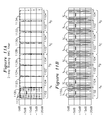
- FIG. 11A (which may be viewed in combination with FIG. 11B ) shows a simplified wavelength plot for the interrogator of FIG. 10 for understanding the invention, where the adjacent AWG responses 1120 and 1122 (used with ⁇ A), 1124 and 1126 (used with ⁇ B), 1128 and 1130 (used with ⁇ C), and lastly 1132 and 1134 (used with ⁇ D) are shown in aggregate response for all channels of each AWG filter.
- the first AWG has a fundamental response 1120 (with individual AWG channel responses 1121 shown for reference), a first aliased response 1124 , a second aliased response 1128 , and a third aliased response 1132 .
- the second AWG has a fundamental response 1122 which is adjacent to the first AWG fundamental response 1120 .
- the second AWG also has a first aliased response 1126 , a second aliased response 1130 , and a third aliased response 1134 .
- FIG. 11B shows the individual AWG wavelength optical outputs for a particular AWG, and also the associated range of each of the narrowband optical FBG sensor reflections generated by string 1006 of FIG. 10 .
- the optical sources 1002 -A through 1002 -D of FIG. 10 generate output optical energy in wavelength ranges shown as ⁇ A, ⁇ B, ⁇ C, and 2 W of FIGS. 11A and 11B , which cover the range of a first AWG and second AWG in a fundamental or aliased response range, as shown.
- FIG. 11C shows a detailed region 1150 of FIG.
- the FBG with response 1161 reflects optical energy generating detector response amplitudes 1162 and 1164 , which may be resolved to a particular associated FBG reflected wavelength.
- the FBG with response 1159 reflects narrowband optical energy which is converted into a detector response 1160 and 1166 , and resolved into a particular wavelength, and the FBG with narrowband response 1163 associated with the second AWG filter may be simultaneously read using the responses of adjacent AWG filter channels 1156 and 1158 , as before.
- the other channels operate in a similar manner, where a particular optical source is enabled, and the response is read from either a fundamental or aliased response of the two AWG filters as a single unit. It is also possible to perform wavelength interrogation using the responses from adjacent AWG filters where the FBG narrowband reflection is at between the two AWG filters. For this case, the two AWG filter responses need to have overlap of the adjacent channel responses, as shown in detail FIG. 11D , where an FBG narrowband FBG reflected wavelength 1171 falls in the range of first AWG filter response 1152 and second AWG filter response 1156 , providing response 1170 associated with a detector in a first AWG and response 1172 associated with a detector in the second AWG.
- An AWG of this construction with 40 channels on a first AWG and 40 channels on a second AWG, with a detector coupled to each AWG channel and the wavelength resolution performed using pairs of adjacent detectors, can thereby simultaneously resolve the wavelength of 79 FBGs, each of which is constrained to operate within the range of the two corresponding adjacent AWG channels.
- FBG sensors 1068 are excited with optical energy, each FBG sensor in that group reflecting optical energy at its specific narrowband wavelength, all of which FBG sensors in group 1068 are simultaneously read using the first aliased response 1124 of the first AWG filter and first aliased response 1026 of the second AWG filter.
- FIG. 12 shows the example of FIG. 10 and with the same reference numbers for identical elements, but with the optical combiners 1003 -A, 1003 -B, and 1003 -C replaced by a Course Wavelength Division Multiplexing (CWDM) add drop multiplexer 1206 .
- the CWDM 1206 typically has lower losses than the splitter combiners 1003 -A through 1003 -C of FIG. 10 .
- the splitter 1031 of FIG. 10 may be replaced by a 2-way CWDM filter 1208 , which would have lower optical losses delivering reflected optical energy to the first AWG 1020 and second AWG 1040 than the splitter 1031 of FIG. 10 .
- a single AWG filter 1020 which has a sufficiently large number of channels is used, such that the aliased response of the lowest wavelength channel is adjacent to the fundamental response of the highest wavelength channel, such that there is no need for the second AWG 1040 and associated detectors 1031 and 1044 .
- the single AWG 1020 provides aliased response which covers the desired optical spectrum in a continuous manner, with each optical source 1002 -A, 1002 -B, 1002 -C and 1002 -D covering each aliased spectrum of the AWG filter 1020 .
- it is less expensive to use multiple AWG filters in arrangements of two as is shown in FIGS. 10 and 12 but it is understood that the aliased response of a single AWG filter can alternatively be used when it becomes economically attractive to do so, or in the integrated optics embodiments described below.
- FIG. 13 shows plots for the individual channel responses of an AWG such as AWG A 1920 of FIG. 10 which resolves an applied wavelength using either a fundamental or aliased response, i.e., half the frequency separation between AWG channels of a single AWG as previously described.
- AWG A 1020 and AWG B 1040 have adjacent, but non-overlapping responses
- each channel response 1302 , 1304 , 1306 , 1308 is associated with a particular AWG output.
- By examination of two adjacent AWG channel responses in range 1320 it is possible to resolve the two adjacent channel responses into a particular wavelength. For example, reading the responses of adjacent channels 1302 and 1304 for wavelength 1342 resolves the applied wavelengths within range 1320 .
- wavelength region 1320 provides optimum wavelength resolution.
- the amplitude response flattens on the high amplitude channel, and the response becomes increasingly attenuated in the adjacent channel (such as below the ⁇ 20 db limits of the plot), which reduces the resolution.
- the wavelength resolution for an applied wavelength at point 1360 would be quite low. It is desired to provide increased wavelength resolution over a larger range of wavelengths.
- FIG. 14 shows the use of AWG A 1020 and AWG B 1040 with interleaved responses according to another aspect of the invention.
- the AWG channel responses are offset by half a channel spacing, i.e., half the frequency separation between AWG channels of a single AWG.
- AWG A 1020 has channel responses 1402 , 1404 , 1406 , and 1408 .
- AWG B 1040 has channel responses 1452 , 1454 , 1456 , and 1458 .
- the greater coverage afforded by the interleaved AWG responses allows for continuous resolution of wavelength in bands 1420 , 1422 , 1424 , and 1426 , as well as 1470 , 1472 , and 1474 .
- Wavelength 1460 which is not resolvable from AWG A 1020 channel 1404 may be now resolved using AWG B 1020 channels 1452 and 1454 associated detectors.
- any other number of such aliased responses is possible in other embodiments of the invention.
- the number of optical sources shown in FIG. 10 as 1002 -A to 1002 -D is set to correspond to the number of aliased responses of the AWG filter 1020 and 1040 in use, however a larger number of optical sources may be used, for example individual optical sources for first AWG 1020 and each of its alias responses in use, and individual optical sources for second AWG 1020 and each of its alias responses in use. Other numbers and combinations of optical sources are also possible.
- the optical sources may be combined using a single optical combiner or multiple optical combiners.
- the sensor string 1006 may be fabricated from a single fiber with FBG sensors arranged in sequence as shown in FIG. 10 , or several strings of sensors may be combined, as long as each FBG sensor operates in a unique wavelength range from any other FBG sensor and has a corresponding optical source.
- the FBGs of the FBG sensor array may be arranged in any order of wavelength, and are shown as organized with broadband source wavelength groupings in FIGS. 10 and 12 for ease of understanding the invention.
- first AWG filter 10 could start with the first channel at 1578.8 nm and end with the 34th channel (with 0.8 nm channel separation) at 1605.2 nm.
- the first AWG filter first channel would then have a first alias response at 1606 nm.
- the interleaving of first and second AWG would thereby provide continuous coverage of the optical spectrum.
- a custom AWG configured for this purpose, including a single AWG with an aliasing response that is non-overlapping to perform the function of the two AWG filters 1020 and 1040 shown in FIG. 10 .
- the invention may be practiced using individual fabricated optical components, or the wavelength interrogator may be fabricated using prior art integrated optic techniques onto a substrate.
- the individual components of wavelength interrogator 1001 of FIG. 10 or wavelength interrogator 1201 of FIG. 12 may be fabricated using integrated optic methods.
- the optical elements are interconnected using optical waveguides fabricated using prior art Silicon on Insulator (SOI) fabrication methods, such as by forming the waveguides from patterned silicon (Si) waveguide cores fabricated over an insulating SiO2 (also known as Silica) cladding, which in turn is fabricated over a Silicon (Si) substrate.
- SOI Silicon on Insulator
- the waveguides may be formed using oxygen ion implantation below the surface of the silicon substrate using the prior art Separation by IMplanted Oxygen (SIMOX) process.
- SIMOX Separation by IMplanted Oxygen
- Another method for forming integrated optic components is the prior art Bond and Etch-back SOI (BESOI), where two wafers to be bonded have an oxidation applied to each surface, followed by bonding of the oxidized surfaces, which form the core of the waveguide, and subsequent thinning of one of the substrates, which forms the cladding of the waveguide.
- BESOI Bond and Etch-back SOI
- Another method is silicon epitaxial growth, where chemical vapor deposition (CVD) is used to form the waveguide core over the substrate, followed by photo etching and additional layers of CVD cladding to form the interconnecting waveguides.
- CVD chemical vapor deposition
- the circulators 1004 , AWG filters 1020 , 1040 , CWDM filter 1208 , combiners 1003 , and optical sources 1002 may be formed, such that the entire interrogator 1001 and 1201 are formed onto a single substrate for cost effectiveness and compact size.
- An optical adapter may be provided to couple to the sensor FBGs 1060 , 1064 , 1068 , and 1074 .
- the individual optical elements of interrogator 1001 and 1201 may be formed from discrete optical elements and interconnected using optical fiber.
Abstract
Description
Claims (23)
Priority Applications (1)
| Application Number | Priority Date | Filing Date | Title |
|---|---|---|---|
| US14/616,488 US9110259B1 (en) | 2013-03-14 | 2015-02-06 | Interleaved aliased AWG filter for continuous wideband wavelength discrimination |
Applications Claiming Priority (2)
| Application Number | Priority Date | Filing Date | Title |
|---|---|---|---|
| US13/830,939 US8983250B2 (en) | 2013-03-14 | 2013-03-14 | AWG filter for wavelength interrogator |
| US14/616,488 US9110259B1 (en) | 2013-03-14 | 2015-02-06 | Interleaved aliased AWG filter for continuous wideband wavelength discrimination |
Related Parent Applications (1)
| Application Number | Title | Priority Date | Filing Date |
|---|---|---|---|
| US13/830,939 Continuation-In-Part US8983250B2 (en) | 2013-03-14 | 2013-03-14 | AWG filter for wavelength interrogator |
Publications (1)
| Publication Number | Publication Date |
|---|---|
| US9110259B1 true US9110259B1 (en) | 2015-08-18 |
Family
ID=53785974
Family Applications (1)
| Application Number | Title | Priority Date | Filing Date |
|---|---|---|---|
| US14/616,488 Active US9110259B1 (en) | 2013-03-14 | 2015-02-06 | Interleaved aliased AWG filter for continuous wideband wavelength discrimination |
Country Status (1)
| Country | Link |
|---|---|
| US (1) | US9110259B1 (en) |
Cited By (23)
| Publication number | Priority date | Publication date | Assignee | Title |
|---|---|---|---|---|
| US20160306113A1 (en) * | 2011-12-30 | 2016-10-20 | Infinera Corporation | Optical communication system having tunable sources |
| EP3144633A1 (en) * | 2015-09-16 | 2017-03-22 | Technobis Group B.V. | Fiber bragg grating interrogator assembly and method for the same |
| US20170328808A1 (en) * | 2014-12-23 | 2017-11-16 | Halliburton Energy Services, Inc | Apparatus and Method for Characterization of FBG Rellector Array |
| US11064592B1 (en) * | 2018-09-28 | 2021-07-13 | Apple Inc. | Systems and methods for wavelength locking in optical sensing systems |
| US11156497B2 (en) | 2017-09-29 | 2021-10-26 | Apple Inc. | Connected epitaxial optical sensing systems comprising a second epitaxial chip with a second light source and a second detector to detect light of a first light source |
| US11158996B2 (en) | 2017-09-28 | 2021-10-26 | Apple Inc. | Laser architectures using quantum well intermixing techniques |
| US11171464B1 (en) | 2018-12-14 | 2021-11-09 | Apple Inc. | Laser integration techniques |
| US11226459B2 (en) | 2018-02-13 | 2022-01-18 | Apple Inc. | Integrated photonics device having integrated edge outcouplers |
| US11231319B1 (en) | 2019-09-09 | 2022-01-25 | Apple Inc. | Athermal wavelength stability monitor using a detraction grating |
| US11320718B1 (en) | 2019-09-26 | 2022-05-03 | Apple Inc. | Cantilever beam waveguide for silicon photonics device |
| US11500154B1 (en) | 2019-10-18 | 2022-11-15 | Apple Inc. | Asymmetric optical power splitting system and method |
| US11506535B1 (en) | 2019-09-09 | 2022-11-22 | Apple Inc. | Diffraction grating design |
| US11525967B1 (en) | 2018-09-28 | 2022-12-13 | Apple Inc. | Photonics integrated circuit architecture |
| US11525958B1 (en) | 2019-09-09 | 2022-12-13 | Apple Inc. | Off-cut wafer with a supported outcoupler |
| US11561346B2 (en) | 2020-09-24 | 2023-01-24 | Apple Inc. | Tunable echelle grating |
| US11579080B2 (en) | 2017-09-29 | 2023-02-14 | Apple Inc. | Resolve path optical sampling architectures |
| US11644618B2 (en) | 2018-06-22 | 2023-05-09 | Apple Inc. | Discrete optical unit on a substrate of an integrated photonics chip |
| US11815719B2 (en) | 2020-09-25 | 2023-11-14 | Apple Inc. | Wavelength agile multiplexing |
| US11835836B1 (en) | 2019-09-09 | 2023-12-05 | Apple Inc. | Mach-Zehnder interferometer device for wavelength locking |
| US11852318B2 (en) | 2020-09-09 | 2023-12-26 | Apple Inc. | Optical system for noise mitigation |
| US11852865B2 (en) | 2020-09-24 | 2023-12-26 | Apple Inc. | Optical system with phase shifting elements |
| US11881678B1 (en) | 2019-09-09 | 2024-01-23 | Apple Inc. | Photonics assembly with a photonics die stack |
| US11906778B2 (en) | 2020-09-25 | 2024-02-20 | Apple Inc. | Achromatic light splitting device with a high V number and a low V number waveguide |
Citations (1)
| Publication number | Priority date | Publication date | Assignee | Title |
|---|---|---|---|---|
| US7903907B1 (en) * | 2008-04-10 | 2011-03-08 | Intelligent Fiber Optic Systems, Inc. | Force and deflection sensor with shell membrane and optical gratings and method of manufacture |
-
2015
- 2015-02-06 US US14/616,488 patent/US9110259B1/en active Active
Patent Citations (1)
| Publication number | Priority date | Publication date | Assignee | Title |
|---|---|---|---|---|
| US7903907B1 (en) * | 2008-04-10 | 2011-03-08 | Intelligent Fiber Optic Systems, Inc. | Force and deflection sensor with shell membrane and optical gratings and method of manufacture |
Cited By (28)
| Publication number | Priority date | Publication date | Assignee | Title |
|---|---|---|---|---|
| US20160306113A1 (en) * | 2011-12-30 | 2016-10-20 | Infinera Corporation | Optical communication system having tunable sources |
| US20170328808A1 (en) * | 2014-12-23 | 2017-11-16 | Halliburton Energy Services, Inc | Apparatus and Method for Characterization of FBG Rellector Array |
| US9909951B2 (en) * | 2014-12-23 | 2018-03-06 | Halliburton Energy Services, Inc. | Apparatus and method for characterization of FBG rellector array |
| EP3144633A1 (en) * | 2015-09-16 | 2017-03-22 | Technobis Group B.V. | Fiber bragg grating interrogator assembly and method for the same |
| US10247880B2 (en) | 2015-09-16 | 2019-04-02 | Technobis Group B. V. | Fiber Bragg grating interrogator assembly and method for the same |
| US11777279B2 (en) | 2017-09-28 | 2023-10-03 | Apple Inc. | Laser architectures using quantum well intermixing techniques |
| US11158996B2 (en) | 2017-09-28 | 2021-10-26 | Apple Inc. | Laser architectures using quantum well intermixing techniques |
| US11156497B2 (en) | 2017-09-29 | 2021-10-26 | Apple Inc. | Connected epitaxial optical sensing systems comprising a second epitaxial chip with a second light source and a second detector to detect light of a first light source |
| US11579080B2 (en) | 2017-09-29 | 2023-02-14 | Apple Inc. | Resolve path optical sampling architectures |
| US11226459B2 (en) | 2018-02-13 | 2022-01-18 | Apple Inc. | Integrated photonics device having integrated edge outcouplers |
| US11644618B2 (en) | 2018-06-22 | 2023-05-09 | Apple Inc. | Discrete optical unit on a substrate of an integrated photonics chip |
| US20210345468A1 (en) * | 2018-09-28 | 2021-11-04 | Apple Inc. | Systems and Methods for Wavelength Locking in Optical Sensing Systems |
| US11832364B2 (en) * | 2018-09-28 | 2023-11-28 | Apple Inc. | Systems and methods for wavelength locking in optical sensing systems |
| US11064592B1 (en) * | 2018-09-28 | 2021-07-13 | Apple Inc. | Systems and methods for wavelength locking in optical sensing systems |
| US11525967B1 (en) | 2018-09-28 | 2022-12-13 | Apple Inc. | Photonics integrated circuit architecture |
| US11171464B1 (en) | 2018-12-14 | 2021-11-09 | Apple Inc. | Laser integration techniques |
| US11506535B1 (en) | 2019-09-09 | 2022-11-22 | Apple Inc. | Diffraction grating design |
| US11525958B1 (en) | 2019-09-09 | 2022-12-13 | Apple Inc. | Off-cut wafer with a supported outcoupler |
| US11231319B1 (en) | 2019-09-09 | 2022-01-25 | Apple Inc. | Athermal wavelength stability monitor using a detraction grating |
| US11835836B1 (en) | 2019-09-09 | 2023-12-05 | Apple Inc. | Mach-Zehnder interferometer device for wavelength locking |
| US11881678B1 (en) | 2019-09-09 | 2024-01-23 | Apple Inc. | Photonics assembly with a photonics die stack |
| US11320718B1 (en) | 2019-09-26 | 2022-05-03 | Apple Inc. | Cantilever beam waveguide for silicon photonics device |
| US11500154B1 (en) | 2019-10-18 | 2022-11-15 | Apple Inc. | Asymmetric optical power splitting system and method |
| US11852318B2 (en) | 2020-09-09 | 2023-12-26 | Apple Inc. | Optical system for noise mitigation |
| US11561346B2 (en) | 2020-09-24 | 2023-01-24 | Apple Inc. | Tunable echelle grating |
| US11852865B2 (en) | 2020-09-24 | 2023-12-26 | Apple Inc. | Optical system with phase shifting elements |
| US11815719B2 (en) | 2020-09-25 | 2023-11-14 | Apple Inc. | Wavelength agile multiplexing |
| US11906778B2 (en) | 2020-09-25 | 2024-02-20 | Apple Inc. | Achromatic light splitting device with a high V number and a low V number waveguide |
Similar Documents
| Publication | Publication Date | Title |
|---|---|---|
| US9110259B1 (en) | Interleaved aliased AWG filter for continuous wideband wavelength discrimination | |
| US8983250B2 (en) | AWG filter for wavelength interrogator | |
| CN1726664B (en) | Optical interrogation system and sensor system | |
| CN100382471C (en) | Method for monitoring optical signal performance in interleaving system and apparatus thereof | |
| US6486984B1 (en) | Wavelength monitor using hybrid approach | |
| CN1835420B (en) | Optical performance monitor | |
| CN100507455C (en) | Intensity modulation type optical fiber sensor multiplexing method | |
| CN106164725A (en) | Adjustable grid follows the tracks of emitter and receptor | |
| JP4971316B2 (en) | Multi-wavelength sensor array | |
| US7302179B2 (en) | Optical performance monitor using co-located switchable fiber bragg grating array | |
| TWI234668B (en) | Fiber Bragg grating sensing system of light intensity and wave-divided multiplex | |
| KR100322125B1 (en) | AWG module and method for monitoring optical signal using AWG module | |
| US7127132B1 (en) | Cascade fiber-optic grating-based sensor apparatus and method | |
| TW200301380A (en) | Optical relay amplifier and wavelength multiplexing device | |
| EP1133082A1 (en) | Optical monitoring system | |
| KR20020000759A (en) | Fibre bragg grating sensors for measuring a physical magnitude | |
| JP3669473B2 (en) | Wavelength measuring device | |
| US6570686B1 (en) | Reference wavelength providing device for performance monitor in WDM optical transmission system | |
| Black et al. | AWG Filter for Wavelength Interrogator | |
| JP2022544522A (en) | Method and system for interrogating a fiber Bragg grating type fiber optic sensor using a tunable optical bandpass filter | |
| KR100965842B1 (en) | Optical add-drop multiplexer for multi-channel | |
| JP2020071238A (en) | Wavelength checker | |
| KR102522885B1 (en) | Reflected light wavelength scanning device including silicon photonics interrogator | |
| KR102295964B1 (en) | Appratus of Measuring Power of Multi-Channel Optical Signal | |
| CN114172580B (en) | Optical sensing network WDM-PON system based on adjustable ONU and signal propagation method |
Legal Events
| Date | Code | Title | Description |
|---|---|---|---|
| AS | Assignment |
Owner name: INTELLIGENT FIBER OPTIC SYSTEMS, INC, CALIFORNIA Free format text: ASSIGNMENT OF ASSIGNORS INTEREST;ASSIGNORS:MOSLEHI, BEHZAD;BLACK, RICHARD J.;SIGNING DATES FROM 20150313 TO 20150320;REEL/FRAME:035250/0669 |
|
| AS | Assignment |
Owner name: INTELLIGENT FIBER OPTIC SYSTEMS, INC, CALIFORNIA Free format text: ASSIGNMENT OF ASSIGNORS INTEREST;ASSIGNORS:SOTOUDEH, VAHID;CHESAVAGE, JAY A.;SIGNING DATES FROM 20150207 TO 20150603;REEL/FRAME:035983/0587 |
|
| STCF | Information on status: patent grant |
Free format text: PATENTED CASE |
|
| FEPP | Fee payment procedure |
Free format text: MAINTENANCE FEE REMINDER MAILED (ORIGINAL EVENT CODE: REM.); ENTITY STATUS OF PATENT OWNER: SMALL ENTITY |
|
| FEPP | Fee payment procedure |
Free format text: SURCHARGE FOR LATE PAYMENT, SMALL ENTITY (ORIGINAL EVENT CODE: M2554); ENTITY STATUS OF PATENT OWNER: SMALL ENTITY |
|
| MAFP | Maintenance fee payment |
Free format text: PAYMENT OF MAINTENANCE FEE, 4TH YR, SMALL ENTITY (ORIGINAL EVENT CODE: M2551); ENTITY STATUS OF PATENT OWNER: SMALL ENTITY Year of fee payment: 4 |
|
| FEPP | Fee payment procedure |
Free format text: MAINTENANCE FEE REMINDER MAILED (ORIGINAL EVENT CODE: REM.); ENTITY STATUS OF PATENT OWNER: SMALL ENTITY |
|
| FEPP | Fee payment procedure |
Free format text: 7.5 YR SURCHARGE - LATE PMT W/IN 6 MO, SMALL ENTITY (ORIGINAL EVENT CODE: M2555); ENTITY STATUS OF PATENT OWNER: SMALL ENTITY |
|
| MAFP | Maintenance fee payment |
Free format text: PAYMENT OF MAINTENANCE FEE, 8TH YR, SMALL ENTITY (ORIGINAL EVENT CODE: M2552); ENTITY STATUS OF PATENT OWNER: SMALL ENTITY Year of fee payment: 8 |