US9049763B1 - LED luminaire driving circuit with high power factor - Google Patents

LED luminaire driving circuit with high power factor Download PDF

Info

Publication number
US9049763B1
US9049763B1 US14/198,752 US201414198752A US9049763B1 US 9049763 B1 US9049763 B1 US 9049763B1 US 201414198752 A US201414198752 A US 201414198752A US 9049763 B1 US9049763 B1 US 9049763B1
Authority
US
United States
Prior art keywords
unit
signal
coupled
output
power switch
Prior art date
Legal status (The legal status is an assumption and is not a legal conclusion. Google has not performed a legal analysis and makes no representation as to the accuracy of the status listed.)
Active
Application number
US14/198,752
Inventor
Hsuang-Chang Chiang
Chao-Tsung Ma
Kun-Feng Chen
Ying-Sun Huang
Current Assignee (The listed assignees may be inaccurate. Google has not performed a legal analysis and makes no representation or warranty as to the accuracy of the list.)
National Chung Shan Institute of Science and Technology NCSIST
Original Assignee
National Chung Shan Institute of Science and Technology NCSIST
Priority date (The priority date is an assumption and is not a legal conclusion. Google has not performed a legal analysis and makes no representation as to the accuracy of the date listed.)
Filing date
Publication date
Application filed by National Chung Shan Institute of Science and Technology NCSIST filed Critical National Chung Shan Institute of Science and Technology NCSIST
Priority to US14/198,752 priority Critical patent/US9049763B1/en
Assigned to CHUNG-SHAN INSTITUTE OF SCIENCE AND TECHNOLOGY reassignment CHUNG-SHAN INSTITUTE OF SCIENCE AND TECHNOLOGY ASSIGNMENT OF ASSIGNORS INTEREST (SEE DOCUMENT FOR DETAILS). Assignors: CHIANG, HSUANG-CHANG, MA, CHAO-TSUNG, HUANG, YING-SUN, CHEN, KUN-FENG
Assigned to NATIONAL CHUNG SHAN INSTITUTE OF SCIENCE AND TECHNOLOGY reassignment NATIONAL CHUNG SHAN INSTITUTE OF SCIENCE AND TECHNOLOGY CHANGE OF NAME (SEE DOCUMENT FOR DETAILS). Assignors: Chung-Shan Institute of Science and Technology, Armaments, Bureau, Ministry of National Defense
Application granted granted Critical
Publication of US9049763B1 publication Critical patent/US9049763B1/en
Active legal-status Critical Current
Anticipated expiration legal-status Critical

Links

Images

Classifications

    • H05B33/0815
    • HELECTRICITY
    • H05ELECTRIC TECHNIQUES NOT OTHERWISE PROVIDED FOR
    • H05BELECTRIC HEATING; ELECTRIC LIGHT SOURCES NOT OTHERWISE PROVIDED FOR; CIRCUIT ARRANGEMENTS FOR ELECTRIC LIGHT SOURCES, IN GENERAL
    • H05B45/00Circuit arrangements for operating light-emitting diodes [LED]
    • H05B45/10Controlling the intensity of the light
    • H05B33/0845
    • HELECTRICITY
    • H05ELECTRIC TECHNIQUES NOT OTHERWISE PROVIDED FOR
    • H05BELECTRIC HEATING; ELECTRIC LIGHT SOURCES NOT OTHERWISE PROVIDED FOR; CIRCUIT ARRANGEMENTS FOR ELECTRIC LIGHT SOURCES, IN GENERAL
    • H05B45/00Circuit arrangements for operating light-emitting diodes [LED]
    • H05B45/30Driver circuits
    • H05B45/37Converter circuits
    • H05B45/3725Switched mode power supply [SMPS]
    • H05B45/385Switched mode power supply [SMPS] using flyback topology

Definitions

  • the present invention relates to the technology fields of LED luminaire driving circuits, and more particularly to an LED luminaire driving circuit with high power factor.
  • LEDs light-emitting diodes
  • more and more families replace the traditional fluorescent lamps by LED lamps due to the issue of Energy Conservation and Carbon Reduction is more and more popular.
  • the power formation of the market electricity is AC power and the LED lamps are driven to emit light by DC power, it is necessary to dispose a power converting device between the market electricity and the LED lamps for converting the AC power to DC power.
  • FIG. 1 there is shown a circuit framework diagram of a BCM flyback converter with variable frequency control.
  • the BCM (Boundary Conduction Mode) flyback converter with variable frequency control 1 a shown by FIG. 1 is a peak-current-mode PWM (pulse width modulation) converter, and the engineers skilled in LED lamp driving circuit field are able to find the following drawbacks of the BCM flyback converter with variable frequency control 1 a from the circuit framework of FIG.
  • PWM pulse width modulation
  • the voltage-sensing circuit 11 a disposed at the input end of the BCM flyback converter with variable frequency control 1 a would produce extra power consumption; and (2) the cut-off time of the secondary side current I D — a of the BCM flyback converter with variable frequency control 1 a is fully decided by the output diode D O — a , such that the cut-off time of the secondary side current I D — a cannot be precisely predicted and controlled.
  • FIG. 2 there is shown the circuit framework diagram of another BCM flyback converter with variable frequency control.
  • the BCM (Boundary Conduction Mode) flyback converter with variable frequency control 1 b shown by FIG. 2 is a constant on-time control converter, and the engineers skilled in LED lamp driving circuit field can find the following drawbacks of the BCM flyback converter with variable frequency control 1 b from the circuit framework of FIG. 2 : the cut-off time of the secondary side current I D — b of the BCM flyback converter with variable frequency control 1 b is fully decided by the output diode D O — b , so the cut-off time of the secondary side current I D — b cannot be precisely predicted and controlled.
  • FIG. 3 which illustrates the circuit framework diagram of a DCM flyback converter with constant frequency control.
  • the DCM (Discontinuous Conduction Mode) flyback converter with constant frequency control 1 c shown by FIG. 3 is a voltage control converter, and the engineers skilled in LED lamp driving circuit field is able to easily know that the DCM flyback converter with constant frequency control 1 c can merely be used for driving low power LED lamps because the DCM flyback converter with constant frequency control 1 c includes higher switching current I Q — C under the same working power.
  • the COT flyback converter with variable frequency control 1 d shown by FIG. 4 is a peak-current-mode PWM (pulse width modulation) converter, and the engineers skilled in LED lamp driving circuit field are able to find that the COT flyback converter with variable frequency control 1 d can be operated under discontinuous conduction mode, boundary conduction mode or continuous conduction mode (CCM); however, the COT flyback converter with variable frequency control 1 d still includes the following drawbacks: the voltage-sensing circuit 11 d disposed at the input end of the COT flyback converter with variable frequency control 1 d would produce extra power consumption.
  • PWM pulse width modulation
  • FIG. 5 illustrates the circuit framework diagram of a constant-frequency control flyback converter.
  • the constant-frequency control flyback converter 1 e shown by FIG. 5 is a current-clamp control converter, and the engineers skilled in LED lamp driving circuit field can easily understand that the constant-frequency control flyback converter 1 e carries out the power factor correction by using the constant current (CC) error amplifier 11 e , the constant voltage (CV) error amplifier 12 e , the opticalcoupler feedback circuit 13 e , the triangle compensation signal V tri , and the power device driving circuit 14 e to produce a PWM driving signal to the power transistor Q PW ′.
  • the constant-frequency control flyback converter 1 e still includes the following drawbacks: the entire manufacturing cost of the constant-frequency control flyback converter 1 e is too expensive because the disposing of the opticalcoupler feedback circuit 13 e.
  • the primary objective of the present invention is to provide an LED luminaire driving circuit with high power factor, which especially integrated with a zero current detecting unit, a feedback unit and an error amplifier unit without using any input-end voltage detecting signal.
  • the LED luminaire driving circuit can be used for driving high power LED lamps, and work without producing any extra power consumption.
  • the another objective of the present invention is to provide an LED luminaire driving circuit with high power factor, which integrated with a zero current detecting unit, a feedback unit and an error amplifier unit.
  • the LED luminaire driving circuit proposed by the present invention does not include any optocoupler feedback circuits, so it is able to effectively reduce the entire circuit manufacturing cost of this LED luminaire driving circuit.
  • this LED luminaire driving circuit can selectively work under CCM operation or DCM operation with high power factor (PF ⁇ 1), and provide stable output voltage signal and output current signal to load end.
  • this LED luminaire driving circuit performs excellent stability and current modulation error rate ( ⁇ +3%).
  • an LED luminaire driving circuit with high power factor comprising:
  • a filter unit coupled to an input source for receiving an AC signal
  • a rectifier unit coupled to the filter unit for receiving the AC signal via the filter unit, and then treats the AC signal with a rectifying process so as to output an input signal
  • a transformer unit coupled to the rectifier unit for receiving the input signal, and then transforms the input signal having a peak input voltage to an output signal having a peak output voltage, so as to output the output signal to an LED lighting unit for making the LED lighting unit emit light;
  • a power switch unit coupled between the rectifier unit and the transformer unit and used for treating the input signal with switching control
  • a zero current detecting unit being coupled to the transformer unit and used for treating the output signal with a zero current detection, so as to output a zero current detection signal
  • a feedback unit being coupled to the zero current detecting unit and the power switch unit, wherein the feedback unit receives a power switch current and the zero current detection signal, and outputting a feedback signal according to the power switch current and the zero current detection signal;
  • an error amplifier unit being coupled to the zero current detecting unit and the feedback unit for receiving the feedback signal, and then outputs an error amplification signal according to the feedback signal;
  • a power switch driving unit being coupled to the power switch unit and the error amplifier unit for receiving the error amplification signal, and then outputs a driving signal to the power switch unit according to the error amplification signal, so as to drive the power switch unit to treat the input signal with switching control.
  • FIG. 1 is a circuit framework diagram of a BCM flyback converter with variable frequency control
  • FIG. 2 is a circuit framework diagram of another BCM flyback converter with variable frequency control
  • FIG. 3 is a circuit framework diagram of a DCM flyback converter with constant frequency control
  • FIG. 4 is a circuit framework diagram of a COT flyback converter with variable frequency control
  • FIG. 5 is a circuit framework diagram of a constant-frequency control flyback converter
  • FIG. 6 is a circuit block diagram of an LED luminaire driving circuit with high power factor according to the present invention.
  • FIG. 7 is a circuit framework diagram of the LED luminaire driving circuit with high power factor according to the present invention.
  • FIG. 8 shows signal waveforms of the LED luminaire driving circuit working under DCM operation
  • FIG. 9 is a plot of an input current as a function of the conduction angle
  • FIG. 10 shows signal waveforms of the LED luminaire driving circuit working under CCM operation
  • FIG. 11 shows curves of the input current and the conduction angle
  • FIG. 12 is a plot of the input current as a function of the conduction angle
  • FIG. 13A and FIG. 13B show simulated signal waveforms of the LED luminaire driving circuit working under CCM operation.
  • FIG. 14A and FIG. 14B show simulated signal waveforms of the LED luminaire driving circuit working under DCM operation.
  • the LED luminaire driving circuit 1 of the present invention includes: a filter unit 10 , a rectifier unit 11 , a transformer unit 12 , an output unit 13 , a power switch unit 15 , a zero current detecting unit 16 , a feedback unit 17 , an error amplifier unit 18 , and a power switch driving unit 19 .
  • FIG. 6 shows a circuit framework diagram of the LED luminaire driving circuit with high power factor.
  • the filter unit 10 is coupled to an input source V S for receiving an AC signal.
  • the filter unit 10 consists of a first capacitor C X1 , a common mode chock winding L CM and a second capacitor C X2 , wherein the first capacitor C X1 is connected across the two input terminals of the common mode chock winding L CM , and the second capacitor C X2 is connected across the two output terminals of the common mode chock winding L CM .
  • the rectifier unit 11 is a bridge rectifier, which is coupled to the filter unit 10 for receiving the AC signal via the filter unit 10 , and then treats the AC signal with a rectifying process so as to output an input signal V in .
  • the transformer unit 12 is coupled to the rectifier unit 11 and has a primary winding coil N p , a secondary winding coil N S and an auxiliary winding coil N a .
  • the transformer unit 12 is used for receiving the input signal V in , and then transforming the input signal V in having a peak input voltage to an output signal V O having a peak output voltage, so as to output the output signal V O to an LED lighting unit 14 for making the LED lighting unit 14 emit light.
  • the output unit 13 is coupled between the transformer unit 12 and the LED lighting unit 14 for outputting the output signal V O to the LED lighting unit 14 .
  • the output unit 13 is consisted of an output diode D O and an output capacitor C O , wherein the output diode D O is coupled to the one terminal of the primary winding coil N p by one end thereof, and the output capacitor C O is coupled to the other end of the output diode D O by one end thereof, moreover the other end of the output capacitor C O is coupled to other terminal of the primary winding coil N p and the LED lighting unit 14 .
  • the power switch unit 15 is a Power Metal-Oxide-Semiconductor Field-Effect Transistor (power MOSFET), and the source terminal of the power MOSFET Q is coupled with a source resistor R S .
  • the power switch unit 15 is coupled between the rectifier unit 11 and the transformer unit 12 and used for treating the input signal V in with switching control.
  • the LED luminaire driving circuit 1 of the present invention includes a zero current detecting unit 16 , which is able to detect the output signal V O via a signal detecting unit 16 a coupled between the transformer unit 12 and the zero current detecting unit 16 . As shown in FIG. 6 and FIG.
  • the signal detecting unit 16 a has at least one resistor (R dect1 , R dect2 ), wherein one end of the resistor (R dect1 , R dect2 ) is coupled to one terminal of the auxiliary winding coil N a , and the other end of the resistor is coupled to the other terminal of the auxiliary winding coil N a and the ground of the LED luminaire driving circuit 1 .
  • the zero current detecting unit 16 is able to output a zero current detection signal Z CD after receiving a detection signal V ded from the signal detecting unit 16 a.
  • the zero current detecting unit 16 consists of a comparator 161 , an adder 162 , an inverter 163 , and a Set/Reset flip flop 164 , wherein the comparator 161 is coupled to the signal detecting unit 16 a for receiving the detection signal V dec .
  • the an adder 162 is coupled between a first input end and an output end of the comparator 161 , moreover the adder 162 is further coupled with a reference signal V REF1 .
  • the inverter 163 is coupled to the output end of the comparator 161
  • the Set/Reset flip flop 164 is respectively coupled to the invertor 163 and the power switch unit 15 by one reset end and one set end thereof.
  • the feedback unit 17 is coupled to the zero current detecting unit 16 and the power switch unit 15 .
  • the feedback unit 17 is used for receiving a power switch current I Q of the power switch unit 15 and the zero current detection signal Z CD , and then outputting a feedback signal V FB according to the power switch current I Q and the zero current detection signal Z CD .
  • the feedback unit 17 includes a low pass filter 171 and a multiplexer 172 , wherein the low pass filter 171 is coupled to power switch unit 15 for receiving the power switch current I Q , so as to treat the power switch current I Q with a low pass filtering process.
  • the multiplexer 172 is coupled to the low pass filter 171 and the zero current detecting unit 16 for receiving the zero current detection signal Z CD and the low-pass-filtered power switch current I Q , so as to output the feedback signal V FB .
  • the feedback unit 17 further includes a relay coupled between the multiplexer 172 and the error amplifier unit 18 .
  • the error amplifier unit 18 is coupled to the zero current detecting unit 16 and the feedback unit 17 for receiving the feedback signal V FB , and then outputs an error amplification signal Vea according to the feedback signal V FB .
  • the power switch driving unit 19 is coupled to the power switch unit 15 and the error amplifier unit 18 for receiving the error amplification signal V ea , so as to output a driving signal V G to the power switch unit 15 according to the error amplification signal Vea; therefore, the power switch unit 15 is able to treat the input signal Vin with switching control according to the driving signal V G .
  • the error amplifier unit 18 consists of a proportional-integral (PI) compensator 181 and a multiplexer 182 , wherein the PI compensator 181 is coupled to the feedback unit 17 for receiving the feedback signal V FB , and the multiplexer 182 is coupled to the power switch driving unit 19 for receiving the driving signal V G .
  • PI proportional-integral
  • the multiplexer 182 is further coupled with a reference current signal I REF , such that the multiplexer 182 is able to output a reference voltage signal V REF to the PI compensator 181 according to the driving signal V G and the reference current signal I REF , and then the PI compensator 181 may output the error amplification signal V ea to a subtractor 191 of the power switch driving unit 19 according to the reference voltage signal V REF and the feedback signal V FB .
  • the subtractor 191 coupled to the error amplifier unit 18 simultaneously receiving the a ripple signal V rip , therefore the subtractor 191 outputs a conversion signal V con to a comparator 192 of the power switch driving unit 19 according to the ripple signal V rip and the error amplification signal V ea .
  • the comparator 192 coupled to the subtractor 191 and the power switch unit 15 , is used for respectively receiving the conversion signal V con and a power switch voltage signal V CS of the power switch unit 15 ; therefore, the comparator 192 would output a comparison signal according to the power switch voltage signal V CS and the conversion signal V con . As shown in FIG. 6 and FIG.
  • the power switch driving unit 19 further includes a Set/Reset flip flop 193 , which is coupled to the output end of the comparator 193 by one reset end thereof; moreover, one set end of the Set/Reset flip flop 193 is coupled with a clock signal CLK, such that the Set/Reset flip flop 193 is able to output the driving signal V G to the power switch unit 15 according the clock signal CLK and the comparison signal received from the comparator 193 .
  • a Set/Reset flip flop 193 which is coupled to the output end of the comparator 193 by one reset end thereof; moreover, one set end of the Set/Reset flip flop 193 is coupled with a clock signal CLK, such that the Set/Reset flip flop 193 is able to output the driving signal V G to the power switch unit 15 according the clock signal CLK and the comparison signal received from the comparator 193 .
  • V con is the conversion signal outputted by the subtractor 191 of the power switch driving unit 19
  • V ea is the error amplification signal V ea outputted by the PI compensator 181 of the error amplifier unit 18
  • T on is the conduction time of the power switch unit 15
  • m a is the slope of the ripple signal V rip
  • m 1 is the slope of the ripple signal V CS of the power MOSFET Q of the power switch unit 15 .
  • the I D marked in FIG. 8 means the diode current of the output diode D O of the output unit 13 .
  • T on V ea /(m 1 +m a ).
  • L p means the self-inductance of the transformer unit 12
  • I pk means the peak value of the power switch current I Q .
  • I S (V ea 2 /2R S T S )*[m 1 /(m 1 +m a ) 2 ].
  • FIG. 11 shows, when the conduction angle is ranged between ⁇ 0 and ⁇ 0 and different slope compensating parameter K S is substituted into above-mentioned formula (4), a plot of the input current I S as a function of the conduction angle can be obtained and shown as FIG. 12 . From the plot of FIG. 12 , it is able to observe that the greater value the slope compensating parameter K S is set, the less distortion the input current I S shows.
  • FIG. 13A and FIG. 13B there are shown simulated signal waveforms of the LED luminaire driving circuit working under CCM operation.
  • the simulated signal waveforms shown by FIG. 13A and FIG. 13B have been proved that the LED luminaire driving circuit 1 proposed by the present invention can provide stable output voltage signal V O and output current signal I O , and simultaneously performs excellent stability and current modulation error rate ( ⁇ 3%).
  • V S 110V rms
  • V S 110V rms
  • FIG. 14A and FIG. 14B there are shown simulated signal waveforms of the LED luminaire driving circuit working under DCM operation.
  • the simulated signal waveforms shown by FIG. 14A and FIG. 14B have been proved that the LED luminaire driving circuit 1 proposed by the present invention can provide stable output voltage signal V O and output current signal I O , and simultaneously performs excellent stability and current modulation error rate ( ⁇ 3%).
  • V S 220V rms
  • V S 220V rms
  • the simulated signal waveforms of FIG. 13A , FIG. 13B , FIG. 14A , and FIG. 14B proves that the LED luminaire driving circuit 1 proposed by the present invention can indeed works under different mode (CDM or DCM) operation with high power factor.

Landscapes

  • Circuit Arrangement For Electric Light Sources In General (AREA)

Abstract

The present invention relates to an LED luminaire driving circuit with high power factor, comprising: a filter unit, a rectifier unit, a transformer unit, a power switch unit, a zero current detecting unit, a feedback unit, an error amplifier unit, and a power switch driving unit. Particularly, the LED luminaire driving circuit proposed by the present invention does not include any optocoupler feedback circuits, so it is able to effectively reduce the entire circuit manufacturing cost of this LED luminaire driving circuit. Moreover, this LED luminaire driving circuit can selectively work under CCM operation or DCM operation with high power factor (PF˜1), and provide stable output voltage signal and output current signal to load end. In addition, this LED luminaire driving circuit performs excellent stability and current modulation error rate (<±3%).

Description

BACKGROUND OF THE INVENTION
1. Field of the Invention
The present invention relates to the technology fields of LED luminaire driving circuits, and more particularly to an LED luminaire driving circuit with high power factor.
2. Description of the Prior Art
Recently, light-emitting diodes (LEDs) are widely applied to be the lighting device in human life. And currently, more and more families replace the traditional fluorescent lamps by LED lamps due to the issue of Energy Conservation and Carbon Reduction is more and more popular. However, since the power formation of the market electricity is AC power and the LED lamps are driven to emit light by DC power, it is necessary to dispose a power converting device between the market electricity and the LED lamps for converting the AC power to DC power.
With reference to FIG. 1, there is shown a circuit framework diagram of a BCM flyback converter with variable frequency control. The BCM (Boundary Conduction Mode) flyback converter with variable frequency control 1 a shown by FIG. 1 is a peak-current-mode PWM (pulse width modulation) converter, and the engineers skilled in LED lamp driving circuit field are able to find the following drawbacks of the BCM flyback converter with variable frequency control 1 a from the circuit framework of FIG. 1: (1) the voltage-sensing circuit 11 a disposed at the input end of the BCM flyback converter with variable frequency control 1 a would produce extra power consumption; and (2) the cut-off time of the secondary side current ID a of the BCM flyback converter with variable frequency control 1 a is fully decided by the output diode DO a, such that the cut-off time of the secondary side current ID a cannot be precisely predicted and controlled.
Please refer to FIG. 2, there is shown the circuit framework diagram of another BCM flyback converter with variable frequency control. The BCM (Boundary Conduction Mode) flyback converter with variable frequency control 1 b shown by FIG. 2 is a constant on-time control converter, and the engineers skilled in LED lamp driving circuit field can find the following drawbacks of the BCM flyback converter with variable frequency control 1 b from the circuit framework of FIG. 2: the cut-off time of the secondary side current ID b of the BCM flyback converter with variable frequency control 1 b is fully decided by the output diode DO b, so the cut-off time of the secondary side current ID b cannot be precisely predicted and controlled.
Referring to FIG. 3, which illustrates the circuit framework diagram of a DCM flyback converter with constant frequency control. The DCM (Discontinuous Conduction Mode) flyback converter with constant frequency control 1 c shown by FIG. 3 is a voltage control converter, and the engineers skilled in LED lamp driving circuit field is able to easily know that the DCM flyback converter with constant frequency control 1 c can merely be used for driving low power LED lamps because the DCM flyback converter with constant frequency control 1 c includes higher switching current IQ C under the same working power.
With reference to FIG. 4, there is shown the circuit framework diagram of a COT flyback converter with variable frequency control. The COT (Constant Off-Time) flyback converter with variable frequency control 1 d shown by FIG. 4 is a peak-current-mode PWM (pulse width modulation) converter, and the engineers skilled in LED lamp driving circuit field are able to find that the COT flyback converter with variable frequency control 1 d can be operated under discontinuous conduction mode, boundary conduction mode or continuous conduction mode (CCM); however, the COT flyback converter with variable frequency control 1 d still includes the following drawbacks: the voltage-sensing circuit 11 d disposed at the input end of the COT flyback converter with variable frequency control 1 d would produce extra power consumption.
Please refer to FIG. 5, which illustrates the circuit framework diagram of a constant-frequency control flyback converter. The constant-frequency control flyback converter 1 e shown by FIG. 5 is a current-clamp control converter, and the engineers skilled in LED lamp driving circuit field can easily understand that the constant-frequency control flyback converter 1 e carries out the power factor correction by using the constant current (CC) error amplifier 11 e, the constant voltage (CV) error amplifier 12 e, the opticalcoupler feedback circuit 13 e, the triangle compensation signal Vtri, and the power device driving circuit 14 e to produce a PWM driving signal to the power transistor QPW′. In spite of that, the constant-frequency control flyback converter 1 e still includes the following drawbacks: the entire manufacturing cost of the constant-frequency control flyback converter 1 e is too expensive because the disposing of the opticalcoupler feedback circuit 13 e.
Accordingly, in view of the conventional LED lamps driving circuits all include drawbacks and shortcomings, the inventor of the present application has made great efforts to make inventive research thereon and eventually provided an LED luminaire driving circuit with high power factor.
SUMMARY OF THE INVENTION
The primary objective of the present invention is to provide an LED luminaire driving circuit with high power factor, which especially integrated with a zero current detecting unit, a feedback unit and an error amplifier unit without using any input-end voltage detecting signal. The LED luminaire driving circuit can be used for driving high power LED lamps, and work without producing any extra power consumption.
The another objective of the present invention is to provide an LED luminaire driving circuit with high power factor, which integrated with a zero current detecting unit, a feedback unit and an error amplifier unit. Particularly, the LED luminaire driving circuit proposed by the present invention does not include any optocoupler feedback circuits, so it is able to effectively reduce the entire circuit manufacturing cost of this LED luminaire driving circuit. Moreover, this LED luminaire driving circuit can selectively work under CCM operation or DCM operation with high power factor (PF˜1), and provide stable output voltage signal and output current signal to load end. In addition, this LED luminaire driving circuit performs excellent stability and current modulation error rate (<+3%).
Accordingly, to achieve the primary objective of the present invention, the inventor of the present invention provides an LED luminaire driving circuit with high power factor, comprising:
a filter unit, coupled to an input source for receiving an AC signal;
a rectifier unit, coupled to the filter unit for receiving the AC signal via the filter unit, and then treats the AC signal with a rectifying process so as to output an input signal;
a transformer unit, coupled to the rectifier unit for receiving the input signal, and then transforms the input signal having a peak input voltage to an output signal having a peak output voltage, so as to output the output signal to an LED lighting unit for making the LED lighting unit emit light;
a power switch unit, coupled between the rectifier unit and the transformer unit and used for treating the input signal with switching control;
a zero current detecting unit, being coupled to the transformer unit and used for treating the output signal with a zero current detection, so as to output a zero current detection signal;
a feedback unit, being coupled to the zero current detecting unit and the power switch unit, wherein the feedback unit receives a power switch current and the zero current detection signal, and outputting a feedback signal according to the power switch current and the zero current detection signal;
an error amplifier unit, being coupled to the zero current detecting unit and the feedback unit for receiving the feedback signal, and then outputs an error amplification signal according to the feedback signal; and
a power switch driving unit, being coupled to the power switch unit and the error amplifier unit for receiving the error amplification signal, and then outputs a driving signal to the power switch unit according to the error amplification signal, so as to drive the power switch unit to treat the input signal with switching control.
BRIEF DESCRIPTION OF THE DRAWINGS
The invention as well as a preferred mode of use and advantages thereof will be best understood by referring to the following detailed description of an illustrative embodiment in conjunction with the accompanying drawings, wherein:
FIG. 1 is a circuit framework diagram of a BCM flyback converter with variable frequency control;
FIG. 2 is a circuit framework diagram of another BCM flyback converter with variable frequency control;
FIG. 3 is a circuit framework diagram of a DCM flyback converter with constant frequency control;
FIG. 4 is a circuit framework diagram of a COT flyback converter with variable frequency control;
FIG. 5 is a circuit framework diagram of a constant-frequency control flyback converter;
FIG. 6 is a circuit block diagram of an LED luminaire driving circuit with high power factor according to the present invention;
FIG. 7 is a circuit framework diagram of the LED luminaire driving circuit with high power factor according to the present invention;
FIG. 8 shows signal waveforms of the LED luminaire driving circuit working under DCM operation;
FIG. 9 is a plot of an input current as a function of the conduction angle;
FIG. 10 shows signal waveforms of the LED luminaire driving circuit working under CCM operation;
FIG. 11 shows curves of the input current and the conduction angle;
FIG. 12 is a plot of the input current as a function of the conduction angle;
FIG. 13A and FIG. 13B show simulated signal waveforms of the LED luminaire driving circuit working under CCM operation; and
FIG. 14A and FIG. 14B show simulated signal waveforms of the LED luminaire driving circuit working under DCM operation.
DETAILED DESCRIPTION OF THE PREFERRED EMBODIMENTS
To more clearly describe an LED luminaire driving circuit with high power factor according to the present invention, embodiments of the present invention will be described in detail with reference to the attached drawings hereinafter.
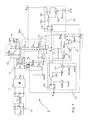
With reference to FIG. 6, there is shown a circuit block diagram of an LED luminaire driving circuit with high power factor according to the present invention. As shown in FIG. 6, the LED luminaire driving circuit 1 of the present invention includes: a filter unit 10, a rectifier unit 11, a transformer unit 12, an output unit 13, a power switch unit 15, a zero current detecting unit 16, a feedback unit 17, an error amplifier unit 18, and a power switch driving unit 19.
Referring to FIG. 6 again, and please simultaneously refer to FIG. 7, which shows a circuit framework diagram of the LED luminaire driving circuit with high power factor. As shown in FIG. 6 and FIG. 7, the filter unit 10 is coupled to an input source VS for receiving an AC signal. The filter unit 10 consists of a first capacitor CX1, a common mode chock winding LCM and a second capacitor CX2, wherein the first capacitor CX1 is connected across the two input terminals of the common mode chock winding LCM, and the second capacitor CX2 is connected across the two output terminals of the common mode chock winding LCM. The rectifier unit 11 is a bridge rectifier, which is coupled to the filter unit 10 for receiving the AC signal via the filter unit 10, and then treats the AC signal with a rectifying process so as to output an input signal Vin.
The transformer unit 12 is coupled to the rectifier unit 11 and has a primary winding coil Np, a secondary winding coil NS and an auxiliary winding coil Na. In the present invention, the transformer unit 12 is used for receiving the input signal Vin, and then transforming the input signal Vin having a peak input voltage to an output signal VO having a peak output voltage, so as to output the output signal VO to an LED lighting unit 14 for making the LED lighting unit 14 emit light.
Inheriting to above description, the output unit 13 is coupled between the transformer unit 12 and the LED lighting unit 14 for outputting the output signal VO to the LED lighting unit 14. As shown in FIG. 7, the output unit 13 is consisted of an output diode DO and an output capacitor CO, wherein the output diode DO is coupled to the one terminal of the primary winding coil Np by one end thereof, and the output capacitor CO is coupled to the other end of the output diode DO by one end thereof, moreover the other end of the output capacitor CO is coupled to other terminal of the primary winding coil Np and the LED lighting unit 14.
The power switch unit 15 is a Power Metal-Oxide-Semiconductor Field-Effect Transistor (power MOSFET), and the source terminal of the power MOSFET Q is coupled with a source resistor RS. The power switch unit 15 is coupled between the rectifier unit 11 and the transformer unit 12 and used for treating the input signal Vin with switching control. Particularly, the LED luminaire driving circuit 1 of the present invention includes a zero current detecting unit 16, which is able to detect the output signal VO via a signal detecting unit 16 a coupled between the transformer unit 12 and the zero current detecting unit 16. As shown in FIG. 6 and FIG. 7, the signal detecting unit 16 a has at least one resistor (Rdect1, Rdect2), wherein one end of the resistor (Rdect1, Rdect2) is coupled to one terminal of the auxiliary winding coil Na, and the other end of the resistor is coupled to the other terminal of the auxiliary winding coil Na and the ground of the LED luminaire driving circuit 1. Thus, the zero current detecting unit 16 is able to output a zero current detection signal ZCD after receiving a detection signal Vded from the signal detecting unit 16 a.
The zero current detecting unit 16 consists of a comparator 161, an adder 162, an inverter 163, and a Set/Reset flip flop 164, wherein the comparator 161 is coupled to the signal detecting unit 16 a for receiving the detection signal Vdec. The an adder 162 is coupled between a first input end and an output end of the comparator 161, moreover the adder 162 is further coupled with a reference signal VREF1. Besides, the inverter 163 is coupled to the output end of the comparator 161, and the Set/Reset flip flop 164 is respectively coupled to the invertor 163 and the power switch unit 15 by one reset end and one set end thereof.
Inheriting to above description, the feedback unit 17 is coupled to the zero current detecting unit 16 and the power switch unit 15. In the present invention, the feedback unit 17 is used for receiving a power switch current IQ of the power switch unit 15 and the zero current detection signal ZCD, and then outputting a feedback signal VFB according to the power switch current IQ and the zero current detection signal ZCD. As shown in FIG. 6 and FIG. 7, the feedback unit 17 includes a low pass filter 171 and a multiplexer 172, wherein the low pass filter 171 is coupled to power switch unit 15 for receiving the power switch current IQ, so as to treat the power switch current IQ with a low pass filtering process. The multiplexer 172 is coupled to the low pass filter 171 and the zero current detecting unit 16 for receiving the zero current detection signal ZCD and the low-pass-filtered power switch current IQ, so as to output the feedback signal VFB. Moreover, the feedback unit 17 further includes a relay coupled between the multiplexer 172 and the error amplifier unit 18.
The error amplifier unit 18 is coupled to the zero current detecting unit 16 and the feedback unit 17 for receiving the feedback signal VFB, and then outputs an error amplification signal Vea according to the feedback signal VFB. In addition, the power switch driving unit 19 is coupled to the power switch unit 15 and the error amplifier unit 18 for receiving the error amplification signal Vea, so as to output a driving signal VG to the power switch unit 15 according to the error amplification signal Vea; therefore, the power switch unit 15 is able to treat the input signal Vin with switching control according to the driving signal VG.
As shown in FIG. 6 and FIG. 7, the error amplifier unit 18 consists of a proportional-integral (PI) compensator 181 and a multiplexer 182, wherein the PI compensator 181 is coupled to the feedback unit 17 for receiving the feedback signal VFB, and the multiplexer 182 is coupled to the power switch driving unit 19 for receiving the driving signal VG. Moreover, the multiplexer 182 is further coupled with a reference current signal IREF, such that the multiplexer 182 is able to output a reference voltage signal VREF to the PI compensator 181 according to the driving signal VG and the reference current signal IREF, and then the PI compensator 181 may output the error amplification signal Vea to a subtractor 191 of the power switch driving unit 19 according to the reference voltage signal VREF and the feedback signal VFB.
Besides the error amplification signal Vea, the subtractor 191 coupled to the error amplifier unit 18 simultaneously receiving the a ripple signal Vrip, therefore the subtractor 191 outputs a conversion signal Vcon to a comparator 192 of the power switch driving unit 19 according to the ripple signal Vrip and the error amplification signal Vea. The comparator 192, coupled to the subtractor 191 and the power switch unit 15, is used for respectively receiving the conversion signal Vcon and a power switch voltage signal VCS of the power switch unit 15; therefore, the comparator 192 would output a comparison signal according to the power switch voltage signal VCS and the conversion signal Vcon. As shown in FIG. 6 and FIG. 7, the power switch driving unit 19 further includes a Set/Reset flip flop 193, which is coupled to the output end of the comparator 193 by one reset end thereof; moreover, one set end of the Set/Reset flip flop 193 is coupled with a clock signal CLK, such that the Set/Reset flip flop 193 is able to output the driving signal VG to the power switch unit 15 according the clock signal CLK and the comparison signal received from the comparator 193.
Therefore, above descriptions have been introduce the detailed circuit framework of the LED luminaire driving circuit 1 proposed by the present invention; Next, in order to prove the practicability and performance of the LED luminaire driving circuit 1, a variety of circuit simulation are completed and the related simulation data are recorded. Please refer to FIG. 8, which shows signal waveforms of the LED luminaire driving circuit working under DCM (Discontinuous Conduction Mode) operation. From the signal waveforms, it is able to derive the following formula (1): Vcon=Vea−maTon=m1Ton. In above-mentioned formula (1), Vcon is the conversion signal outputted by the subtractor 191 of the power switch driving unit 19, Vea is the error amplification signal Vea outputted by the PI compensator 181 of the error amplifier unit 18, and Ton is the conduction time of the power switch unit 15, ma is the slope of the ripple signal Vrip, and m1 is the slope of the ripple signal VCS of the power MOSFET Q of the power switch unit 15. Moreover, the ID marked in FIG. 8 means the diode current of the output diode DO of the output unit 13.
Since m1=(RS*VS)/LP and Ipk=(Ton*m1)/RS, the Ton can be calculated by the formula of Ton=Vea/(m1+ma). Herein Lp means the self-inductance of the transformer unit 12 and Ipk means the peak value of the power switch current IQ. Moreover, because input current IS is equal to the average value of the power switch current IQ in a switching period, the input current IS can be calculated by using the formula of IS=(Ipk*Ton)/2TS; wherein TS is the switching period of the power MOSFET Q of the power switch unit 15. Subsequently, it is able to derive the following formula (2): IS=(Vea 2/2RSTS)*[m1/(m1+ma)2]. Eventually, after letting ma=KSM1,max=KSRS(Vsm/Lp) and substituting different slope compensating parameter KS and slope ma into above-mentioned formula (2), a plot of the input current IS as a function of the conduction angle can be obtained and shown as FIG. 9. From the plot of FIG. 9, it is able to observe that the greater value the slope compensating parameter KS is set, the less distortion the input current IS shows.
Continuously referring to FIG. 10, which shows signal waveforms of the LED luminaire driving circuit working under CCM (continuous conduction mode) operation. From FIG. 10, it is able to derive the following formula (3): ΔIpk=(m1*Ton)/RS. Because input current IS is equal to the average value of the power switch current IQ in a switching period, the input current IS can be calculated by using the following formula (4): IS=Ia(Ton/TS)+(ΔIpkTon)/2TS, wherein the LED luminaire circuit 1 of the present invention would work under DCM operation when Ia<Ipk. Moreover, as FIG. 11 shows, when the conduction angle is ranged between θ0 and π−θ0 and different slope compensating parameter KS is substituted into above-mentioned formula (4), a plot of the input current IS as a function of the conduction angle can be obtained and shown as FIG. 12. From the plot of FIG. 12, it is able to observe that the greater value the slope compensating parameter KS is set, the less distortion the input current IS shows.
Please refer to FIG. 13A and FIG. 13B, there are shown simulated signal waveforms of the LED luminaire driving circuit working under CCM operation. The simulated signal waveforms shown by FIG. 13A and FIG. 13B have been proved that the LED luminaire driving circuit 1 proposed by the present invention can provide stable output voltage signal VO and output current signal IO, and simultaneously performs excellent stability and current modulation error rate (<±3%). In addition, from FIG. 13A, it can find that the power factor (PF) of the LED luminaire driving circuit 1 working under CCM operation (i.e., VS=110Vrms) reaches to 0.991, and the working current ILED of the LED lighting unit 14 oppositely reaches to 519 mA.
Moreover, please refer to FIG. 14A and FIG. 14B, there are shown simulated signal waveforms of the LED luminaire driving circuit working under DCM operation. The simulated signal waveforms shown by FIG. 14A and FIG. 14B have been proved that the LED luminaire driving circuit 1 proposed by the present invention can provide stable output voltage signal VO and output current signal IO, and simultaneously performs excellent stability and current modulation error rate (<±3%). In addition, from FIG. 14A, it can find that the power factor (PF) of the LED luminaire driving circuit 1 working under DCM operation (i.e., VS=220Vrms) reaches to 0.953, and the working current ILED of the LED lighting unit 14 oppositely reaches to 501 mA. Therefore, the simulated signal waveforms of FIG. 13A, FIG. 13B, FIG. 14A, and FIG. 14B proves that the LED luminaire driving circuit 1 proposed by the present invention can indeed works under different mode (CDM or DCM) operation with high power factor.
The above description is made on embodiments of the present invention. However, the embodiments are not intended to limit scope of the present invention, and all equivalent implementations or alterations within the spirit of the present invention still fall within the scope of the present invention.

Claims (13)

What is claimed is:
1. An LED luminaire driving circuit with high power factor, comprising:
a filter unit, being coupled to an input source for receiving an AC signal;
a rectifier unit, being coupled to the filter unit for receiving the AC signal via the filter unit, and then treats the AC signal with a rectifying process so as to output an input signal;
a transformer unit, being coupled to the rectifier unit for receiving the input signal, and transforming the input signal having a peak input voltage to an output signal having a peak output voltage, so as to output the output signal to an LED lighting unit for making the LED lighting unit emit light;
a power switch unit, being coupled between the rectifier unit and the transformer unit and used for treating the input signal with switching control;
a zero current detecting unit, being coupled to the transformer unit and used for treating the output signal with a zero current detection, so as to output a zero current detection signal;
a feedback unit, being coupled to the zero current detecting unit and the power switch unit, wherein the feedback unit receives a power switch current of the power switch unit and the zero current detection signal, and outputting a feedback signal according to the power switch current and the zero current detection signal; wherein the feedback unit comprises:
a low pass filter, being coupled to power switch unit for receiving the power switch current, so as to treat the power switch current with a low pass filtering process; and
a multiplexer, being coupled to the low pass filter and the zero current detecting unit for receiving the zero current detection signal and the low-pass-filtered power switch current, so as to output the feedback signal;
an error amplifier unit, being coupled to the zero current detecting unit and the feedback unit for receiving the feedback signal, and then outputs an error amplification signal according to the feedback signal; and
a power switch driving unit, being coupled to the power switch unit and the error amplifier unit for receiving the error amplification signal, and then outputs a driving signal to the power switch unit according to the error amplification signal, so as to drive the power switch unit to treat the input signal with switching control.
2. The LED luminaire driving circuit with high power factor of claim 1, wherein the power switch unit comprises a Power Metal-Oxide-Semiconductor Field-Effect Transistor (power MOSFET), and the source terminal of the power MOSFET being coupled with a source resistor.
3. The LED luminaire driving circuit with high power factor of claim 1, wherein filter unit comprises a first capacitor, a common mode chock winding and a second capacitor, in which the first capacitor is connected across the two input terminals of the common mode chock winding, and the second capacitor being connected across the two output terminals of the common mode chock winding.
4. The LED luminaire driving circuit with high power factor of claim 1, wherein the rectifier unit is a bridge rectifier.
5. The LED luminaire driving circuit with high power factor of claim 1, wherein the feedback unit further comprises a relay coupled between the multiplexer and the error amplifier unit.
6. The LED luminaire driving circuit with high power factor of claim 1, wherein the error amplifier unit comprises:
a proportional-integral (PI) compensator, being coupled to the feedback unit for receiving the feedback signal; and
a multiplexer, being coupled to the power switch driving unit for receiving the driving signal, moreover the multiplexer further be coupled with a reference current signal, such that the multiplexer is able to output a reference voltage signal to the PI compensator according to the driving signal and the reference current signal, and then the PI compensator may output the error amplification signal according to the reference voltage signal and the feedback signal.
7. The LED luminaire driving circuit with high power factor of claim 1, wherein the power switch driving unit comprises:
a subtractor, being coupled to the error amplifier unit for receiving the error amplification signal, moreover the subtractor further be coupled with a ripple signal, such that the subtractor is able to output a conversion signal according to the ripple signal and the error amplification signal;
a comparator, being coupled to the subtractor and the power switch unit for receiving the conversion signal and a power switch voltage signal of the power switch unit, respectively; therefore the comparator may output a comparison signal according to the power switch voltage signal and the conversion signal; and
a Set/Reset flip flop, being coupled to the output end of the comparator by one reset end thereof, moreover one set end of the Set/Reset flip flop is coupled with a clock signal, such that the Set/Reset flip flop is able to output the driving signal to the power switch unit according the clock signal and the comparison signal received from the comparator.
8. The LED luminaire driving circuit with high power factor of claim 1, further comprising: an output unit, being coupled between the transformer unit and the LED lighting unit, wherein the output unit is used for outputting the output signal to the LED lighting unit for making the LED lighting unit emit light.
9. The LED luminaire driving circuit with high power factor of claim 8, further comprising: a signal detecting unit, being coupled between the transformer unit and the zero current detecting unit, wherein the signal detecting unit is used for detecting the output signal, so as to output a detection signal to the zero current detecting unit.
10. The LED luminaire driving circuit with high power factor of claim 9, wherein the zero current detecting unit comprises:
a comparator, being coupled to the signal detecting unit for receiving the detection signal, and having a first input end, a second input end and an output end;
an adder, being coupled between the first input end and the output end of the comparator, and the adder further being coupled with a reference signal;
an inverter, being coupled to the output end of the comparator; and
a Set/Reset flip flop, being respectively coupled to the invertor and the power switch unit by one reset end and one set end thereof.
11. The LED luminaire driving circuit with high power factor of claim 9, wherein the transformer unit has a primary winding coil, a secondary winding coil and an auxiliary winding coil.
12. The LED luminaire driving circuit with high power factor of claim 11, wherein the output unit comprises:
an output diode, being coupled to the one terminal of the primary winding coil by one end thereof; and
an output capacitor, being coupled to the other end of the output diode by one end thereof, moreover the other end of the output capacitor is coupled to other terminal of the primary winding coil and the LED lighting unit.
13. The LED luminaire driving circuit with high power factor of claim 11, wherein the signal detecting unit has at least one resistor, in which one end of the resistor is coupled to one terminal of the auxiliary winding coil, and the other end of the resistor being coupled to the other terminal of the auxiliary winding coil and the ground of the LED luminaire driving circuit with high power factor.
US14/198,752 2014-03-06 2014-03-06 LED luminaire driving circuit with high power factor Active US9049763B1 (en)

Priority Applications (1)

Application Number Priority Date Filing Date Title
US14/198,752 US9049763B1 (en) 2014-03-06 2014-03-06 LED luminaire driving circuit with high power factor

Applications Claiming Priority (1)

Application Number Priority Date Filing Date Title
US14/198,752 US9049763B1 (en) 2014-03-06 2014-03-06 LED luminaire driving circuit with high power factor

Publications (1)

Publication Number Publication Date
US9049763B1 true US9049763B1 (en) 2015-06-02

Family

ID=53190822

Family Applications (1)

Application Number Title Priority Date Filing Date
US14/198,752 Active US9049763B1 (en) 2014-03-06 2014-03-06 LED luminaire driving circuit with high power factor

Country Status (1)

Country Link
US (1) US9049763B1 (en)

Cited By (5)

* Cited by examiner, † Cited by third party
Publication number Priority date Publication date Assignee Title
CN105682303A (en) * 2016-04-05 2016-06-15 深圳市莱福德光电有限公司 Two-transistor flyback single-stage PFC LED circuit
TWI608759B (en) * 2015-09-14 2017-12-11 System and method for current regulation in light emitting diode lighting systems
CN108449837A (en) * 2018-04-13 2018-08-24 深圳市崧盛电子股份有限公司 A kind of LED adjusting control circuits
CN113163554A (en) * 2021-04-27 2021-07-23 广东尚研电子科技股份有限公司 LED lamp driving circuit, control method and electronic equipment
CN115987392A (en) * 2023-02-16 2023-04-18 南昌大学 POE-based high-speed visible light communication system and method

Citations (4)

* Cited by examiner, † Cited by third party
Publication number Priority date Publication date Assignee Title
US6009000A (en) * 1999-02-05 1999-12-28 The Aerospace Corporation Shared-bus current sharing parallel connected current-mode DC to DC converters
US6504315B2 (en) * 2000-02-10 2003-01-07 Fairchild Korea Semiconductor Ltd. Lamp system with electronic ballast
US20110199793A1 (en) * 2010-01-29 2011-08-18 Naixing Kuang Switching mode power supply with primary side control
US20120019714A1 (en) * 2010-07-20 2012-01-26 Akinori Hiramatu Led lighting device with chopper circuit and dimming control method

Patent Citations (4)

* Cited by examiner, † Cited by third party
Publication number Priority date Publication date Assignee Title
US6009000A (en) * 1999-02-05 1999-12-28 The Aerospace Corporation Shared-bus current sharing parallel connected current-mode DC to DC converters
US6504315B2 (en) * 2000-02-10 2003-01-07 Fairchild Korea Semiconductor Ltd. Lamp system with electronic ballast
US20110199793A1 (en) * 2010-01-29 2011-08-18 Naixing Kuang Switching mode power supply with primary side control
US20120019714A1 (en) * 2010-07-20 2012-01-26 Akinori Hiramatu Led lighting device with chopper circuit and dimming control method

Cited By (17)

* Cited by examiner, † Cited by third party
Publication number Priority date Publication date Assignee Title
US10595369B2 (en) 2015-09-14 2020-03-17 On-Bright Electronics (Shanghai) Co., Ltd. Systems and methods for current regulation in light-emitting-diode lighting systems
TWI608759B (en) * 2015-09-14 2017-12-11 System and method for current regulation in light emitting diode lighting systems
US9872347B2 (en) 2015-09-14 2018-01-16 On-Bright Electronics (Shanghai) Co., Ltd. Systems and methods for current regulation in light-emitting-diode lighting systems
US9883556B2 (en) 2015-09-14 2018-01-30 On-Bright Electronics (Shanghai) Co., Ltd. Systems and methods for current regulation in light-emitting-diode lighting systems
US11336177B2 (en) 2015-09-14 2022-05-17 On-Bright Electronics (Shanghai) Co., Ltd. Systems and methods for current regulation in light-emitting-diode lighting systems
US10244592B2 (en) 2015-09-14 2019-03-26 On-Bright Electronics (Shanghai) Co., Ltd. Systems and methods for current regulation in light-emitting-diode lighting systems
US10244593B2 (en) 2015-09-14 2019-03-26 On-Bright Electronics (Shanghai) Co., Ltd. Systems and methods for current regulation in light-emitting-diode lighting systems
US10285228B2 (en) 2015-09-14 2019-05-07 On-Bright Electronics (Shanghai) Co., Ltd. Systems and methods for current regulation in light-emitting-diode lighting systems
US10806003B2 (en) 2015-09-14 2020-10-13 On-Bright Electronics (Shanghai) Co., Ltd. Systems and methods for current regulation in light-emitting-diode lighting systems
US10779373B2 (en) 2015-09-14 2020-09-15 On-Bright Electronics (Shanghai) Co., Ltd. Systems and methods for current regulation in light-emitting-diode lighting systems
CN105682303B (en) * 2016-04-05 2019-07-12 深圳市莱福德光电有限公司 A kind of LED circuit of the single- stage PFC of double-transistor flyback
CN105682303A (en) * 2016-04-05 2016-06-15 深圳市莱福德光电有限公司 Two-transistor flyback single-stage PFC LED circuit
WO2019196695A1 (en) * 2018-04-13 2019-10-17 深圳市崧盛电子股份有限公司 Led dimming control circuit
CN108449837B (en) * 2018-04-13 2019-08-23 深圳市崧盛电子股份有限公司 A kind of LED adjusting control circuit
CN108449837A (en) * 2018-04-13 2018-08-24 深圳市崧盛电子股份有限公司 A kind of LED adjusting control circuits
CN113163554A (en) * 2021-04-27 2021-07-23 广东尚研电子科技股份有限公司 LED lamp driving circuit, control method and electronic equipment
CN115987392A (en) * 2023-02-16 2023-04-18 南昌大学 POE-based high-speed visible light communication system and method

Similar Documents

Publication Publication Date Title
US9907130B2 (en) High-efficiency LED driver and driving method
JP3187637U (en) Ceiling light using non-insulated driver circuit
JP5584089B2 (en) Drive circuit with increased power factor
KR100950913B1 (en) DC/DC Converter
US9485819B2 (en) Single stage LED driver system, control circuit and associated control method
JP5761301B2 (en) Lighting device and lighting apparatus
US9049763B1 (en) LED luminaire driving circuit with high power factor
KR20120083845A (en) Led driving device and led lighting device
CA2960663A1 (en) High-power single-stage led driver with bipolar ripple cancellation
TWI474593B (en) Power supply apparatus with power factor correction and pulse width modulation mechanism and method thereof
US10492254B2 (en) Power supply circuit and LED driving circuit
US9036378B2 (en) Power conversion system with adjustable frequency
US20150303813A1 (en) Ac-to-dc power converting device
JP2017504934A (en) Power circuit and dimming control method for LED lighting device
KR20110136537A (en) Led driving circuit and method for protecting from high voltage and driving with constant current
CN102611316A (en) Flyback converter controlled constant-current output circuit and method
Chansri et al. A high power LED driver with Class D ZVS series resonant converter
JP2019029351A (en) Illumination system
TWI458389B (en) Dynamically adjusting dimming range driving apparatus and method thereof
Sekhar et al. Input Regulated Soft Switched Ripple Free Current LED Driver
JP2012029534A (en) Power supply device, and illumination device having the same
JP2017107777A (en) Lighting device and luminaire having the same
JP2016201194A (en) LED lighting device
CN104935165A (en) Power supply device
CN104869711A (en) Resonance-type large-power multipath output LED drive power supply

Legal Events

Date Code Title Description
AS Assignment

Owner name: CHUNG-SHAN INSTITUTE OF SCIENCE AND TECHNOLOGY, TA

Free format text: ASSIGNMENT OF ASSIGNORS INTEREST;ASSIGNORS:CHIANG, HSUANG-CHANG;MA, CHAO-TSUNG;CHEN, KUN-FENG;AND OTHERS;SIGNING DATES FROM 20140207 TO 20140225;REEL/FRAME:032362/0848

AS Assignment

Owner name: NATIONAL CHUNG SHAN INSTITUTE OF SCIENCE AND TECHN

Free format text: CHANGE OF NAME;ASSIGNOR:CHUNG-SHAN INSTITUTE OF SCIENCE AND TECHNOLOGY, ARMAMENTS, BUREAU, MINISTRY OF NATIONAL DEFENSE;REEL/FRAME:035453/0379

Effective date: 20140129

STCF Information on status: patent grant

Free format text: PATENTED CASE

MAFP Maintenance fee payment

Free format text: PAYMENT OF MAINTENANCE FEE, 4TH YEAR, LARGE ENTITY (ORIGINAL EVENT CODE: M1551); ENTITY STATUS OF PATENT OWNER: LARGE ENTITY

Year of fee payment: 4

MAFP Maintenance fee payment

Free format text: PAYMENT OF MAINTENANCE FEE, 8TH YEAR, LARGE ENTITY (ORIGINAL EVENT CODE: M1552); ENTITY STATUS OF PATENT OWNER: LARGE ENTITY

Year of fee payment: 8