US9024300B2 - Manufacture of graphene-based apparatus - Google Patents
Manufacture of graphene-based apparatus Download PDFInfo
- Publication number
- US9024300B2 US9024300B2 US12/779,436 US77943610A US9024300B2 US 9024300 B2 US9024300 B2 US 9024300B2 US 77943610 A US77943610 A US 77943610A US 9024300 B2 US9024300 B2 US 9024300B2
- Authority
- US
- United States
- Prior art keywords
- flat
- graphene layer
- layer
- graphene
- substrate
- Prior art date
- Legal status (The legal status is an assumption and is not a legal conclusion. Google has not performed a legal analysis and makes no representation as to the accuracy of the status listed.)
- Active, expires
Links
- OKTJSMMVPCPJKN-UHFFFAOYSA-N Carbon Chemical compound [C] OKTJSMMVPCPJKN-UHFFFAOYSA-N 0.000 title claims abstract description 133
- 229910021389 graphene Inorganic materials 0.000 title claims abstract description 133
- 238000004519 manufacturing process Methods 0.000 title description 17
- 239000000758 substrate Substances 0.000 claims abstract description 67
- 230000015572 biosynthetic process Effects 0.000 claims description 3
- 238000005411 Van der Waals force Methods 0.000 claims description 2
- 239000010410 layer Substances 0.000 description 115
- XUIMIQQOPSSXEZ-UHFFFAOYSA-N Silicon Chemical compound [Si] XUIMIQQOPSSXEZ-UHFFFAOYSA-N 0.000 description 5
- 239000003989 dielectric material Substances 0.000 description 5
- 238000000034 method Methods 0.000 description 5
- 229910052710 silicon Inorganic materials 0.000 description 5
- 239000010703 silicon Substances 0.000 description 5
- RYGMFSIKBFXOCR-UHFFFAOYSA-N Copper Chemical compound [Cu] RYGMFSIKBFXOCR-UHFFFAOYSA-N 0.000 description 4
- 230000008021 deposition Effects 0.000 description 4
- 230000005669 field effect Effects 0.000 description 4
- CSCPPACGZOOCGX-UHFFFAOYSA-N Acetone Chemical compound CC(C)=O CSCPPACGZOOCGX-UHFFFAOYSA-N 0.000 description 2
- PXHVJJICTQNCMI-UHFFFAOYSA-N Nickel Chemical compound [Ni] PXHVJJICTQNCMI-UHFFFAOYSA-N 0.000 description 2
- 230000003042 antagnostic effect Effects 0.000 description 2
- 239000004020 conductor Substances 0.000 description 2
- 229910052802 copper Inorganic materials 0.000 description 2
- 239000010949 copper Substances 0.000 description 2
- 239000011889 copper foil Substances 0.000 description 2
- 239000013078 crystal Substances 0.000 description 2
- 239000002019 doping agent Substances 0.000 description 2
- 238000005530 etching Methods 0.000 description 2
- GKOZUEZYRPOHIO-UHFFFAOYSA-N iridium atom Chemical compound [Ir] GKOZUEZYRPOHIO-UHFFFAOYSA-N 0.000 description 2
- 239000002184 metal Substances 0.000 description 2
- 229910052751 metal Inorganic materials 0.000 description 2
- 239000002356 single layer Substances 0.000 description 2
- 238000001816 cooling Methods 0.000 description 1
- 230000001419 dependent effect Effects 0.000 description 1
- 238000010438 heat treatment Methods 0.000 description 1
- 239000011229 interlayer Substances 0.000 description 1
- 239000007788 liquid Substances 0.000 description 1
- 238000012986 modification Methods 0.000 description 1
- 230000004048 modification Effects 0.000 description 1
- 229920000642 polymer Polymers 0.000 description 1
Images


Classifications
-
- H—ELECTRICITY
- H01—ELECTRIC ELEMENTS
- H01L—SEMICONDUCTOR DEVICES NOT COVERED BY CLASS H10
- H01L29/00—Semiconductor devices specially adapted for rectifying, amplifying, oscillating or switching and having potential barriers; Capacitors or resistors having potential barriers, e.g. a PN-junction depletion layer or carrier concentration layer; Details of semiconductor bodies or of electrodes thereof ; Multistep manufacturing processes therefor
- H01L29/02—Semiconductor bodies ; Multistep manufacturing processes therefor
- H01L29/12—Semiconductor bodies ; Multistep manufacturing processes therefor characterised by the materials of which they are formed
- H01L29/16—Semiconductor bodies ; Multistep manufacturing processes therefor characterised by the materials of which they are formed including, apart from doping materials or other impurities, only elements of Group IV of the Periodic Table
- H01L29/1606—Graphene
-
- B—PERFORMING OPERATIONS; TRANSPORTING
- B32—LAYERED PRODUCTS
- B32B—LAYERED PRODUCTS, i.e. PRODUCTS BUILT-UP OF STRATA OF FLAT OR NON-FLAT, e.g. CELLULAR OR HONEYCOMB, FORM
- B32B15/00—Layered products comprising a layer of metal
- B32B15/20—Layered products comprising a layer of metal comprising aluminium or copper
-
- B—PERFORMING OPERATIONS; TRANSPORTING
- B32—LAYERED PRODUCTS
- B32B—LAYERED PRODUCTS, i.e. PRODUCTS BUILT-UP OF STRATA OF FLAT OR NON-FLAT, e.g. CELLULAR OR HONEYCOMB, FORM
- B32B27/00—Layered products comprising a layer of synthetic resin
- B32B27/06—Layered products comprising a layer of synthetic resin as the main or only constituent of a layer, which is next to another layer of the same or of a different material
-
- B—PERFORMING OPERATIONS; TRANSPORTING
- B32—LAYERED PRODUCTS
- B32B—LAYERED PRODUCTS, i.e. PRODUCTS BUILT-UP OF STRATA OF FLAT OR NON-FLAT, e.g. CELLULAR OR HONEYCOMB, FORM
- B32B3/00—Layered products comprising a layer with external or internal discontinuities or unevennesses, or a layer of non-planar shape; Layered products comprising a layer having particular features of form
- B32B3/10—Layered products comprising a layer with external or internal discontinuities or unevennesses, or a layer of non-planar shape; Layered products comprising a layer having particular features of form characterised by a discontinuous layer, i.e. formed of separate pieces of material
-
- B—PERFORMING OPERATIONS; TRANSPORTING
- B32—LAYERED PRODUCTS
- B32B—LAYERED PRODUCTS, i.e. PRODUCTS BUILT-UP OF STRATA OF FLAT OR NON-FLAT, e.g. CELLULAR OR HONEYCOMB, FORM
- B32B7/00—Layered products characterised by the relation between layers; Layered products characterised by the relative orientation of features between layers, or by the relative values of a measurable parameter between layers, i.e. products comprising layers having different physical, chemical or physicochemical properties; Layered products characterised by the interconnection of layers
- B32B7/04—Interconnection of layers
- B32B7/06—Interconnection of layers permitting easy separation
-
- B—PERFORMING OPERATIONS; TRANSPORTING
- B32—LAYERED PRODUCTS
- B32B—LAYERED PRODUCTS, i.e. PRODUCTS BUILT-UP OF STRATA OF FLAT OR NON-FLAT, e.g. CELLULAR OR HONEYCOMB, FORM
- B32B7/00—Layered products characterised by the relation between layers; Layered products characterised by the relative orientation of features between layers, or by the relative values of a measurable parameter between layers, i.e. products comprising layers having different physical, chemical or physicochemical properties; Layered products characterised by the interconnection of layers
- B32B7/04—Interconnection of layers
- B32B7/10—Interconnection of layers at least one layer having inter-reactive properties
-
- B—PERFORMING OPERATIONS; TRANSPORTING
- B32—LAYERED PRODUCTS
- B32B—LAYERED PRODUCTS, i.e. PRODUCTS BUILT-UP OF STRATA OF FLAT OR NON-FLAT, e.g. CELLULAR OR HONEYCOMB, FORM
- B32B9/00—Layered products comprising a layer of a particular substance not covered by groups B32B11/00 - B32B29/00
- B32B9/005—Layered products comprising a layer of a particular substance not covered by groups B32B11/00 - B32B29/00 comprising one layer of ceramic material, e.g. porcelain, ceramic tile
- B32B9/007—Layered products comprising a layer of a particular substance not covered by groups B32B11/00 - B32B29/00 comprising one layer of ceramic material, e.g. porcelain, ceramic tile comprising carbon, e.g. graphite, composite carbon
-
- B—PERFORMING OPERATIONS; TRANSPORTING
- B32—LAYERED PRODUCTS
- B32B—LAYERED PRODUCTS, i.e. PRODUCTS BUILT-UP OF STRATA OF FLAT OR NON-FLAT, e.g. CELLULAR OR HONEYCOMB, FORM
- B32B9/00—Layered products comprising a layer of a particular substance not covered by groups B32B11/00 - B32B29/00
- B32B9/04—Layered products comprising a layer of a particular substance not covered by groups B32B11/00 - B32B29/00 comprising such particular substance as the main or only constituent of a layer, which is next to another layer of the same or of a different material
- B32B9/041—Layered products comprising a layer of a particular substance not covered by groups B32B11/00 - B32B29/00 comprising such particular substance as the main or only constituent of a layer, which is next to another layer of the same or of a different material of metal
-
- B—PERFORMING OPERATIONS; TRANSPORTING
- B32—LAYERED PRODUCTS
- B32B—LAYERED PRODUCTS, i.e. PRODUCTS BUILT-UP OF STRATA OF FLAT OR NON-FLAT, e.g. CELLULAR OR HONEYCOMB, FORM
- B32B9/00—Layered products comprising a layer of a particular substance not covered by groups B32B11/00 - B32B29/00
- B32B9/04—Layered products comprising a layer of a particular substance not covered by groups B32B11/00 - B32B29/00 comprising such particular substance as the main or only constituent of a layer, which is next to another layer of the same or of a different material
- B32B9/045—Layered products comprising a layer of a particular substance not covered by groups B32B11/00 - B32B29/00 comprising such particular substance as the main or only constituent of a layer, which is next to another layer of the same or of a different material of synthetic resin
-
- H—ELECTRICITY
- H01—ELECTRIC ELEMENTS
- H01L—SEMICONDUCTOR DEVICES NOT COVERED BY CLASS H10
- H01L21/00—Processes or apparatus adapted for the manufacture or treatment of semiconductor or solid state devices or of parts thereof
- H01L21/02—Manufacture or treatment of semiconductor devices or of parts thereof
- H01L21/02104—Forming layers
- H01L21/02365—Forming inorganic semiconducting materials on a substrate
- H01L21/02518—Deposited layers
- H01L21/02521—Materials
- H01L21/02524—Group 14 semiconducting materials
- H01L21/02527—Carbon, e.g. diamond-like carbon
-
- H—ELECTRICITY
- H01—ELECTRIC ELEMENTS
- H01L—SEMICONDUCTOR DEVICES NOT COVERED BY CLASS H10
- H01L21/00—Processes or apparatus adapted for the manufacture or treatment of semiconductor or solid state devices or of parts thereof
- H01L21/02—Manufacture or treatment of semiconductor devices or of parts thereof
- H01L21/04—Manufacture or treatment of semiconductor devices or of parts thereof the devices having potential barriers, e.g. a PN junction, depletion layer or carrier concentration layer
- H01L21/18—Manufacture or treatment of semiconductor devices or of parts thereof the devices having potential barriers, e.g. a PN junction, depletion layer or carrier concentration layer the devices having semiconductor bodies comprising elements of Group IV of the Periodic Table or AIIIBV compounds with or without impurities, e.g. doping materials
- H01L21/185—Joining of semiconductor bodies for junction formation
- H01L21/187—Joining of semiconductor bodies for junction formation by direct bonding
-
- H—ELECTRICITY
- H01—ELECTRIC ELEMENTS
- H01L—SEMICONDUCTOR DEVICES NOT COVERED BY CLASS H10
- H01L21/00—Processes or apparatus adapted for the manufacture or treatment of semiconductor or solid state devices or of parts thereof
- H01L21/67—Apparatus specially adapted for handling semiconductor or electric solid state devices during manufacture or treatment thereof; Apparatus specially adapted for handling wafers during manufacture or treatment of semiconductor or electric solid state devices or components ; Apparatus not specifically provided for elsewhere
- H01L21/683—Apparatus specially adapted for handling semiconductor or electric solid state devices during manufacture or treatment thereof; Apparatus specially adapted for handling wafers during manufacture or treatment of semiconductor or electric solid state devices or components ; Apparatus not specifically provided for elsewhere for supporting or gripping
- H01L21/6835—Apparatus specially adapted for handling semiconductor or electric solid state devices during manufacture or treatment thereof; Apparatus specially adapted for handling wafers during manufacture or treatment of semiconductor or electric solid state devices or components ; Apparatus not specifically provided for elsewhere for supporting or gripping using temporarily an auxiliary support
-
- H—ELECTRICITY
- H01—ELECTRIC ELEMENTS
- H01L—SEMICONDUCTOR DEVICES NOT COVERED BY CLASS H10
- H01L29/00—Semiconductor devices specially adapted for rectifying, amplifying, oscillating or switching and having potential barriers; Capacitors or resistors having potential barriers, e.g. a PN-junction depletion layer or carrier concentration layer; Details of semiconductor bodies or of electrodes thereof ; Multistep manufacturing processes therefor
- H01L29/66—Types of semiconductor device ; Multistep manufacturing processes therefor
- H01L29/66007—Multistep manufacturing processes
- H01L29/66075—Multistep manufacturing processes of devices having semiconductor bodies comprising group 14 or group 13/15 materials
- H01L29/66227—Multistep manufacturing processes of devices having semiconductor bodies comprising group 14 or group 13/15 materials the devices being controllable only by the electric current supplied or the electric potential applied, to an electrode which does not carry the current to be rectified, amplified or switched, e.g. three-terminal devices
- H01L29/66409—Unipolar field-effect transistors
- H01L29/66477—Unipolar field-effect transistors with an insulated gate, i.e. MISFET
- H01L29/66742—Thin film unipolar transistors
-
- H—ELECTRICITY
- H01—ELECTRIC ELEMENTS
- H01L—SEMICONDUCTOR DEVICES NOT COVERED BY CLASS H10
- H01L29/00—Semiconductor devices specially adapted for rectifying, amplifying, oscillating or switching and having potential barriers; Capacitors or resistors having potential barriers, e.g. a PN-junction depletion layer or carrier concentration layer; Details of semiconductor bodies or of electrodes thereof ; Multistep manufacturing processes therefor
- H01L29/66—Types of semiconductor device ; Multistep manufacturing processes therefor
- H01L29/68—Types of semiconductor device ; Multistep manufacturing processes therefor controllable by only the electric current supplied, or only the electric potential applied, to an electrode which does not carry the current to be rectified, amplified or switched
- H01L29/76—Unipolar devices, e.g. field effect transistors
- H01L29/772—Field effect transistors
- H01L29/778—Field effect transistors with two-dimensional charge carrier gas channel, e.g. HEMT ; with two-dimensional charge-carrier layer formed at a heterojunction interface
- H01L29/7781—Field effect transistors with two-dimensional charge carrier gas channel, e.g. HEMT ; with two-dimensional charge-carrier layer formed at a heterojunction interface with inverted single heterostructure, i.e. with active layer formed on top of wide bandgap layer, e.g. IHEMT
-
- H—ELECTRICITY
- H01—ELECTRIC ELEMENTS
- H01L—SEMICONDUCTOR DEVICES NOT COVERED BY CLASS H10
- H01L29/00—Semiconductor devices specially adapted for rectifying, amplifying, oscillating or switching and having potential barriers; Capacitors or resistors having potential barriers, e.g. a PN-junction depletion layer or carrier concentration layer; Details of semiconductor bodies or of electrodes thereof ; Multistep manufacturing processes therefor
- H01L29/66—Types of semiconductor device ; Multistep manufacturing processes therefor
- H01L29/68—Types of semiconductor device ; Multistep manufacturing processes therefor controllable by only the electric current supplied, or only the electric potential applied, to an electrode which does not carry the current to be rectified, amplified or switched
- H01L29/76—Unipolar devices, e.g. field effect transistors
- H01L29/772—Field effect transistors
- H01L29/78—Field effect transistors with field effect produced by an insulated gate
- H01L29/786—Thin film transistors, i.e. transistors with a channel being at least partly a thin film
- H01L29/78645—Thin film transistors, i.e. transistors with a channel being at least partly a thin film with multiple gate
- H01L29/78648—Thin film transistors, i.e. transistors with a channel being at least partly a thin film with multiple gate arranged on opposing sides of the channel
-
- H—ELECTRICITY
- H01—ELECTRIC ELEMENTS
- H01L—SEMICONDUCTOR DEVICES NOT COVERED BY CLASS H10
- H01L29/00—Semiconductor devices specially adapted for rectifying, amplifying, oscillating or switching and having potential barriers; Capacitors or resistors having potential barriers, e.g. a PN-junction depletion layer or carrier concentration layer; Details of semiconductor bodies or of electrodes thereof ; Multistep manufacturing processes therefor
- H01L29/66—Types of semiconductor device ; Multistep manufacturing processes therefor
- H01L29/68—Types of semiconductor device ; Multistep manufacturing processes therefor controllable by only the electric current supplied, or only the electric potential applied, to an electrode which does not carry the current to be rectified, amplified or switched
- H01L29/76—Unipolar devices, e.g. field effect transistors
- H01L29/772—Field effect transistors
- H01L29/78—Field effect transistors with field effect produced by an insulated gate
- H01L29/786—Thin film transistors, i.e. transistors with a channel being at least partly a thin film
- H01L29/78684—Thin film transistors, i.e. transistors with a channel being at least partly a thin film having a semiconductor body comprising semiconductor materials of Group IV not being silicon, or alloys including an element of the group IV, e.g. Ge, SiN alloys, SiC alloys
-
- H—ELECTRICITY
- H01—ELECTRIC ELEMENTS
- H01L—SEMICONDUCTOR DEVICES NOT COVERED BY CLASS H10
- H01L29/00—Semiconductor devices specially adapted for rectifying, amplifying, oscillating or switching and having potential barriers; Capacitors or resistors having potential barriers, e.g. a PN-junction depletion layer or carrier concentration layer; Details of semiconductor bodies or of electrodes thereof ; Multistep manufacturing processes therefor
- H01L29/66—Types of semiconductor device ; Multistep manufacturing processes therefor
- H01L29/68—Types of semiconductor device ; Multistep manufacturing processes therefor controllable by only the electric current supplied, or only the electric potential applied, to an electrode which does not carry the current to be rectified, amplified or switched
- H01L29/76—Unipolar devices, e.g. field effect transistors
- H01L29/772—Field effect transistors
- H01L29/78—Field effect transistors with field effect produced by an insulated gate
- H01L29/786—Thin film transistors, i.e. transistors with a channel being at least partly a thin film
- H01L29/78696—Thin film transistors, i.e. transistors with a channel being at least partly a thin film characterised by the structure of the channel, e.g. multichannel, transverse or longitudinal shape, length or width, doping structure, or the overlap or alignment between the channel and the gate, the source or the drain, or the contacting structure of the channel
-
- B—PERFORMING OPERATIONS; TRANSPORTING
- B32—LAYERED PRODUCTS
- B32B—LAYERED PRODUCTS, i.e. PRODUCTS BUILT-UP OF STRATA OF FLAT OR NON-FLAT, e.g. CELLULAR OR HONEYCOMB, FORM
- B32B2457/00—Electrical equipment
-
- H—ELECTRICITY
- H01—ELECTRIC ELEMENTS
- H01L—SEMICONDUCTOR DEVICES NOT COVERED BY CLASS H10
- H01L2221/00—Processes or apparatus adapted for the manufacture or treatment of semiconductor or solid state devices or of parts thereof covered by H01L21/00
- H01L2221/67—Apparatus for handling semiconductor or electric solid state devices during manufacture or treatment thereof; Apparatus for handling wafers during manufacture or treatment of semiconductor or electric solid state devices or components; Apparatus not specifically provided for elsewhere
- H01L2221/683—Apparatus for handling semiconductor or electric solid state devices during manufacture or treatment thereof; Apparatus for handling wafers during manufacture or treatment of semiconductor or electric solid state devices or components; Apparatus not specifically provided for elsewhere for supporting or gripping
- H01L2221/68304—Apparatus for handling semiconductor or electric solid state devices during manufacture or treatment thereof; Apparatus for handling wafers during manufacture or treatment of semiconductor or electric solid state devices or components; Apparatus not specifically provided for elsewhere for supporting or gripping using temporarily an auxiliary support
- H01L2221/6835—Apparatus for handling semiconductor or electric solid state devices during manufacture or treatment thereof; Apparatus for handling wafers during manufacture or treatment of semiconductor or electric solid state devices or components; Apparatus not specifically provided for elsewhere for supporting or gripping using temporarily an auxiliary support used as a support during build up manufacturing of active devices
-
- H—ELECTRICITY
- H01—ELECTRIC ELEMENTS
- H01L—SEMICONDUCTOR DEVICES NOT COVERED BY CLASS H10
- H01L2221/00—Processes or apparatus adapted for the manufacture or treatment of semiconductor or solid state devices or of parts thereof covered by H01L21/00
- H01L2221/67—Apparatus for handling semiconductor or electric solid state devices during manufacture or treatment thereof; Apparatus for handling wafers during manufacture or treatment of semiconductor or electric solid state devices or components; Apparatus not specifically provided for elsewhere
- H01L2221/683—Apparatus for handling semiconductor or electric solid state devices during manufacture or treatment thereof; Apparatus for handling wafers during manufacture or treatment of semiconductor or electric solid state devices or components; Apparatus not specifically provided for elsewhere for supporting or gripping
- H01L2221/68304—Apparatus for handling semiconductor or electric solid state devices during manufacture or treatment thereof; Apparatus for handling wafers during manufacture or treatment of semiconductor or electric solid state devices or components; Apparatus not specifically provided for elsewhere for supporting or gripping using temporarily an auxiliary support
- H01L2221/68368—Apparatus for handling semiconductor or electric solid state devices during manufacture or treatment thereof; Apparatus for handling wafers during manufacture or treatment of semiconductor or electric solid state devices or components; Apparatus not specifically provided for elsewhere for supporting or gripping using temporarily an auxiliary support used in a transfer process involving at least two transfer steps, i.e. including an intermediate handle substrate
-
- Y—GENERAL TAGGING OF NEW TECHNOLOGICAL DEVELOPMENTS; GENERAL TAGGING OF CROSS-SECTIONAL TECHNOLOGIES SPANNING OVER SEVERAL SECTIONS OF THE IPC; TECHNICAL SUBJECTS COVERED BY FORMER USPC CROSS-REFERENCE ART COLLECTIONS [XRACs] AND DIGESTS
- Y10—TECHNICAL SUBJECTS COVERED BY FORMER USPC
- Y10T—TECHNICAL SUBJECTS COVERED BY FORMER US CLASSIFICATION
- Y10T428/00—Stock material or miscellaneous articles
- Y10T428/24—Structurally defined web or sheet [e.g., overall dimension, etc.]
- Y10T428/24802—Discontinuous or differential coating, impregnation or bond [e.g., artwork, printing, retouched photograph, etc.]
- Y10T428/24851—Intermediate layer is discontinuous or differential
-
- Y—GENERAL TAGGING OF NEW TECHNOLOGICAL DEVELOPMENTS; GENERAL TAGGING OF CROSS-SECTIONAL TECHNOLOGIES SPANNING OVER SEVERAL SECTIONS OF THE IPC; TECHNICAL SUBJECTS COVERED BY FORMER USPC CROSS-REFERENCE ART COLLECTIONS [XRACs] AND DIGESTS
- Y10—TECHNICAL SUBJECTS COVERED BY FORMER USPC
- Y10T—TECHNICAL SUBJECTS COVERED BY FORMER US CLASSIFICATION
- Y10T428/00—Stock material or miscellaneous articles
- Y10T428/30—Self-sustaining carbon mass or layer with impregnant or other layer
Definitions
- Embodiments of the present invention relate to manufacture of graphene-based apparatus.
- they relate to manufacture of graphene-based electronic devices or circuits and/or structures for the manufacture of graphene-based electronic devices or circuits.
- Graphene has a potentially very high mobility when compared with silicon. It would therefore be desirable to mass produce electronic devices or integrated circuits that use graphene as an electric current channel rather than silicon. However, it is not possible to reuse the scalable mass manufacturing techniques used for mass producing silicon-based electronic devices or circuits to mass produce graphene-based electronic devices or circuits.
- an apparatus comprising:
- an apparatus comprising:
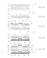
- FIGS. 1A to 1D schematically illustrate operations in manufacturing an apparatus which may be an intermediate structure in the manufacture of an electronic apparatus or integrated circuit;
- FIGS. 2A to 2E schematically illustrate operations in manufacturing the electronic apparatus starting from the intermediate structure
- FIG. 3 schematically illustrates an example embodiment where a dielectric layer intervenes between the first graphene layer and the second graphene layer;
- FIG. 4 schematically illustrates an example of a ring oscillator
- FIG. 5 schematically illustrates an example of an inverter.
- FIGS. 1A , 1 B, 1 C and 1 D schematically illustrate operations in manufacturing an apparatus 70 which is an intermediate structure in the manufacture of an electronic apparatus 72 ( FIG. 2E ).
- the electronic apparatus 72 may be an integrated circuit.
- FIG. 1A illustrates forming a first component 5 comprising a first graphene layer 20 on a first substrate 10 .
- the first substrate 10 is a sacrificial substrate used for the formation of the first graphene layer 20 .
- the first substrate 10 is present in the final structure of the apparatus 70 but is subsequently removed during manufacture of the electronic apparatus 72 ( FIG. 2B ).
- the first substrate 10 may, for example, be any suitable substrate on which graphene can be formed. It may be a crystal or molecular structure. It may be a metal such as a copper foil, or nickel foil or iridium foil.
- the first graphene layer 20 may be a monolayer or consist of a few graphene layers.
- the first graphene layer 20 may be undoped or, alternatively, it may be doped with a p-type or n-type dopant. The doping can be also done in “patterns”, where some parts of the first graphene layer 20 are doped p-type and other parts n-type.
- the first graphene layer 20 has as exposed flat surface 50 .
- FIGS. 1B and 1C illustrate forming a second component 7 comprising a second graphene layer 21 on a second substrate 12 .
- a second graphene layer 21 is formed on a sacrificial substrate 30 . Then a second substrate 12 is formed over the second graphene layer 21 .
- the sacrificial substrate 30 is used for the formation of the second graphene layer 21 and will be subsequently removed during manufacture of the apparatus 70 ( FIG. 1C ).
- the sacrificial substrate 30 may, for example, be any suitable substrate on which graphene can be formed. It may be a crystal or molecular structure. It may be a metal such as a copper foil, or nickel foil or iridium foil.
- the second graphene layer 21 may be a monolayer or consist of a few graphene layers.
- the second graphene layer may be undoped or, alternatively, it may be doped with a p-type or n-type dopant.
- the doping can be also done in “patterns”, where some parts of the second graphene layer 21 are doped p-type and other parts n-type.
- the second substrate 12 is a transfer substrate which is present in the final structure of the apparatus 70 . It is subsequently used during manufacture of the electronic apparatus 72 ( FIG. 2D ) for the flip transfer of at least the combination of at least the first and second graphene layers to a third substrate 23 and is then removed.
- the second substrate 12 may be a removable support polymer.
- the sacrificial substrate 30 is removed to form the second component 7 exposing a flat surface 51 of the second graphene layer 21 .
- the sacrificial substrate 30 is copper it is removed by etching.
- the first component 5 and the second component 7 are joined so that the first substrate 10 and the second substrate 12 are on opposite exterior surfaces of the resultant structure 70 .
- the first graphene layer 20 of the first component 5 and the second graphene layer 21 of the second component part 7 are brought into contact and pressed together.
- the graphene layers adhere as a result of Van der Waals forces. Adhesion between the layers may be improved using a drop of acetone or other liquid on the graphene layers and letting it dry before joining them. Heating and cooling may be used to improve adhesion.
- the first graphene layer 20 directly contacts the second graphene layer 21 .
- a dielectric layer 25 may intervene between the first graphene layer 20 and the second graphene layer 21 as illustrated in FIG. 3 .
- first graphene layer 20 is formed independently of the second graphene layer 21 the layers may have an arbitrary stacking order.
- a specific stacking order between the graphene layers is optional and is not required.
- the lattices for the first graphene layer 20 and the second graphene layer 21 may be rotated and shifted with a random angle and shift, which are not necessarily the ones found in graphitic multilayers
- the illustrated resultant apparatus 70 is a stacked structure 71 comprising: a first substrate 10 having a flat surface 2 ; a flat first graphene layer 20 adjacent and contacting the flat surface 2 of the first substrate 10 ; a flat second graphene layer 21 adjacent (and optionally contacting) the flat first graphene layer 20 ; and a second substrate 12 having a flat surface 3 adjacent and contacting the flat second graphene layer 21 .
- the flat layers and the planar interfaces between the layers are artifacts of the manufacturing process.
- FIGS. 2A to 2E schematically illustrate operations in manufacturing an electronic apparatus 72 using the apparatus 70 as a starting structure as illustrated in FIG. 2A .
- the apparatus 72 is an integrated transistor device.
- the apparatus 70 illustrated in FIG. 2A is the same as that illustrated in FIG. 1D . It is an ordered stacked structure 71 comprising, in order: a first substrate 10 ; a flat first graphene layer 20 ; a second graphene layer 21 ; and a second substrate 12 .
- FIG. 2B illustrates removing the first substrate 10 to expose the first graphene layer 20 that has a flat surface 52 . If the first substrate is copper it may be removed by etching.
- FIG. 2C illustrates forming a flat first patterned layer 22 adjacent and in contact with the first graphene layer 20 .
- the first patterned layer 22 comprises patterned gate electrodes 43 , 45 associated with the first graphene layer 20 , respective dielectric layers 42 , 44 between the patterned gate electrodes 43 , 45 and the first graphene layer 20 , and source/drain electrodes 40 .
- the graphene layers 20 , 21 may be patterned before selective deposition of dielectric to form gate dielectrics 42 , 44 and the selective deposition of conductive material to form bottom gate electrodes 43 , 45 and source/drain electrodes 40 .
- the patterned bottom gate electrodes 43 , 45 are local to one electronic device (conductive channel) each and are not common to or shared between all integrated electronic devices/channels.
- the first patterned layer 22 is a planar layer having a flat surface adjacent the flat surface 52 of the first graphene layer 20 and a flat exposed surface 53 .
- FIG. 2D illustrates that next a third substrate 23 is provided adjacent and in contact with the first patterned layer 22 . Then the structure is flipped so that the third substrate 23 becomes a supporting base. Then the second substrate 12 is removed exposing a flat surface 55 of the second graphene layer 21 .
- FIG. 2E illustrates forming a flat second patterned layer 24 adjacent and in contact with the second graphene layer 21 .
- the second patterned layer 24 comprises patterned gate electrodes 63 , 65 associated with the second graphene layer 21 , respective dielectric layers 62 , 64 between the patterned gate electrodes 63 , 65 and the second graphene layer 21 , and source/drain electrodes 60 .
- the electrodes, gates and dielectric layers may or may not be the same shape and in the same position as in the first patterned layer 22 .
- gate dielectrics 62 , 64 may be used to form gate dielectrics 62 , 64 and selective deposition of conductive material may be used to form top gate electrodes 63 , 65 and source/drain electrodes 60 .
- the gate dielectrics 62 , 64 may be less than 10 nm thick. They may be thinner and/or may have a higher dielectric constant than the gate dielectrics 42 , 44 of the bottom gate electrodes or they may be similar to the gate dielectrics 42 , 44 to maintain symmetry between the top transistors and bottom transistors.
- the patterned top gate electrodes 63 , 65 are local to one or more integrated electronic devices (channels) each but are not typically common to or shared between all integrated electronic devices (channels).
- the second patterned layer 24 is a planar layer in this example having a flat surface adjacent the flat surface 55 of the second graphene layer 21 and a flat exposed surface 54 .
- the resultant structure is an apparatus 72 comprising: an ordered stacked structure 74 comprising, in order:
- the flat layers and the planar interfaces between the layers are artifacts of the manufacturing process.
- the graphene layers may be etched through so that in the final structure at least some of the source/drain electrodes 60 make galvanic contact with at least some of the underlying source/drain electrodes 40 . That is there are source/drain electrodes that are common to the lower patterned layer 22 and the upper patterned layer 24 .
- the structure 72 can be used as a first field effect device, which has two parallel channels 20 , 21 controlled by applying a voltage to the gates 45 , 63 , in series with a second field effect device, which has two parallel channels 20 , 21 controlled by applying a voltage to the gates 43 , 65 .
- the gates 63 , 65 , 43 , 45 may be configured for independent control. Alternatively they may be configured for dependent control.
- the gates 63 , 45 may be interconnected so that the same input voltage Vin is applied to both gates.
- the graphene layers may be doped differently (intra-layer differential doping).
- the upper channel provided by the second graphene layer 21 may be doped to opposite type (n- or p . . . ) than the lower channel provided by the first graphene layer 20 .
- the gates 63 , 45 may be interconnected so that the opposite input voltages are applied to both gates.
- he graphene layers may be doped similarly: the upper channel provided by the second graphene layer 21 may be doped to similar type (n- or p . . . ) as the lower channel provided by the first graphene layer 20 .
- the first field effect device and the second field effect device may be configured for antagonistic inverter operation.
- the doping of the first graphene layer 20 changes between the first device and the second device and the doping of the second graphene layer 21 changes between the first device and the second device (inter-layer differential doping).
- the gates 63 , 65 may be interconnected so that the same input voltage Vin is applied to both gates 63 , 65 .
- the gates 43 , 45 may be interconnected so that the same input voltage is applied to both gates 63 , 65 , which is the same input voltage Vin if the first and second graphene layers are similarly doped and different if the first and second layers are oppositely doped.
- FIG. 5 schematically illustrates an example of an inverter 81 .
- the inverter comprises a series combination of a first transistor 91 and a second transistor 92 .
- the first and second transistors may be formed as described with reference to FIGS. 1A-1D and 2 A- 2 E as an integrated circuit with a common substrate 23 .
- top gates 63 , 65 are interconnected so that a common input voltage Vin is applied to both top gates.
- the first transistor 91 is configured to operate as an on/off transistor and the second transistor 92 is configured to operate as an off/on transistor.
- the first transistor 91 is on and the second transistor 92 is off.
- the first transistor 91 is off and the second transistor 92 is on.
- the antagonistic operation of the first transistor 91 and the second transistor 92 may, for example, be achieved by using differential channel doping between the first transistor 91 and the second transistor 92 which may affect one or more of the graphene layers 20 , 21 and/or by applying different voltages to the back gate electrodes 43 , 45 .
- FIG. 4 schematically illustrates an example of a ring oscillator comprising multiple inverters.
- seven inverters 81 are connected in series in a loop.
- the output of each inverter 81 is provided as an input to the next inverter in the series.
- the output of the last inverter in the series is not only provided as an input to the first inverter 81 in the series but is also provided as an output signal to a buffer 82 comprising two series connected inverters 82 .
- the series of inverters 81 may be integrated in a single circuit so that they share a common substrate 23 .
- the apparatus 72 is a module.
- module refers to a unit or apparatus that excludes certain parts/components that would be added by an end manufacturer or a user.
- the blocks illustrated in the Figs may represent operations in a method.
- the illustration of a particular order to the blocks does not necessarily imply that there is a required or preferred order for the blocks and the order and arrangement of the block may be varied. Furthermore, it may be possible for some operations to be omitted.
Landscapes
- Engineering & Computer Science (AREA)
- Microelectronics & Electronic Packaging (AREA)
- Power Engineering (AREA)
- Ceramic Engineering (AREA)
- Physics & Mathematics (AREA)
- General Physics & Mathematics (AREA)
- Condensed Matter Physics & Semiconductors (AREA)
- Computer Hardware Design (AREA)
- Manufacturing & Machinery (AREA)
- Chemical & Material Sciences (AREA)
- Carbon And Carbon Compounds (AREA)
- Thin Film Transistor (AREA)
- Semiconductor Memories (AREA)
Abstract
Description
- a stacked structure comprising:
- a first substrate having a flat surface;
- a flat first graphene layer adjacent the flat surface of the first substrate;
- a flat second graphene layer adjacent the flat first graphene layer; and
- a second substrate having a flat surface adjacent the flat second graphene layer.
- forming a first component comprising a first graphene layer on a first substrate;
- forming a second component by
- forming a second graphene layer on a sacrificial substrate;
- forming a second substrate over the second graphene layer; and
- removing the sacrificial substrate; and
- joining the first component and the second component so that the first substrate and the second substrate are on opposite exterior surfaces of the resultant structure.
- a stacked structure comprising:
- a substrate having a flat upper surface;
- a flat lower patterned layer overlying the flat upper surface of the substrate and comprising at least one patterned electrode;
- a flat lower graphene layer overlying the flat lower patterned layer;
- a flat upper graphene layer overlying the flat lower graphene layer; and
- a flat upper patterned layer overlying the flat upper graphene layer and comprising at least one patterned electrode.
- removing a first substrate to expose a first graphene layer from a stacked structure comprising:
- a first substrate;
- first and second graphene layers, wherein the first graphene layer is adjacent the first substrate; and
- a second substrate adjacent the second graphene layer;
- forming a first patterned layer adjacent the first graphene layer;
- providing a third substrate adjacent the first patterned layer;
- removing the second substrate;
- forming a second patterned layer adjacent the second graphene layer.
-
- a
substrate 23 having a flatupper surface 55; - a flat lower
patterned layer 22 overlying the flatupper surface 55 of thesubstrate 23 and comprising at least onepatterned electrode - a flat
lower graphene layer 20 overlying the flat lowerpatterned layer 22; - a flat
upper graphene layer 21 overlying the flatlower graphene layer 20; and - a flat upper
patterned layer 24 overlying the flatupper graphene layer 21 and comprising at least onepatterned electrode
- a
Claims (16)
Priority Applications (4)
| Application Number | Priority Date | Filing Date | Title |
|---|---|---|---|
| US12/779,436 US9024300B2 (en) | 2010-05-13 | 2010-05-13 | Manufacture of graphene-based apparatus |
| PCT/IB2011/052087 WO2011141885A1 (en) | 2010-05-13 | 2011-05-12 | Manufacture of graphene-based apparatus |
| EP11780297.5A EP2548228A4 (en) | 2010-05-13 | 2011-05-12 | Manufacture of graphene-based apparatus |
| CN201180023806.7A CN102934230B (en) | 2010-05-13 | 2011-05-12 | Based on the manufacture of the device of Graphene |
Applications Claiming Priority (1)
| Application Number | Priority Date | Filing Date | Title |
|---|---|---|---|
| US12/779,436 US9024300B2 (en) | 2010-05-13 | 2010-05-13 | Manufacture of graphene-based apparatus |
Publications (2)
| Publication Number | Publication Date |
|---|---|
| US20110278545A1 US20110278545A1 (en) | 2011-11-17 |
| US9024300B2 true US9024300B2 (en) | 2015-05-05 |
Family
ID=44910956
Family Applications (1)
| Application Number | Title | Priority Date | Filing Date |
|---|---|---|---|
| US12/779,436 Active 2032-04-28 US9024300B2 (en) | 2010-05-13 | 2010-05-13 | Manufacture of graphene-based apparatus |
Country Status (4)
| Country | Link |
|---|---|
| US (1) | US9024300B2 (en) |
| EP (1) | EP2548228A4 (en) |
| CN (1) | CN102934230B (en) |
| WO (1) | WO2011141885A1 (en) |
Cited By (2)
| Publication number | Priority date | Publication date | Assignee | Title |
|---|---|---|---|---|
| US10852256B2 (en) * | 2015-10-28 | 2020-12-01 | Nokia Technologies Oy | Apparatus and associated methods for computed tomography |
| US11440307B2 (en) | 2018-12-28 | 2022-09-13 | Palo Alto Research Center Incorporated | Method and system for mass assembly of thin-film materials |
Families Citing this family (19)
| Publication number | Priority date | Publication date | Assignee | Title |
|---|---|---|---|---|
| US20110314840A1 (en) * | 2010-06-24 | 2011-12-29 | Hamid-Reza Jahangiri-Famenini | Various methods for industrial scale production of graphene and new devices/instruments to achieve the latter |
| US20120021224A1 (en) * | 2010-07-23 | 2012-01-26 | Clean Energy Labs, Llc | Graphene/graphene oxide platelet composite membranes and methods and devices thereof |
| US8895417B2 (en) * | 2011-11-29 | 2014-11-25 | International Business Machines Corporation | Reducing contact resistance for field-effect transistor devices |
| US8633055B2 (en) * | 2011-12-13 | 2014-01-21 | International Business Machines Corporation | Graphene field effect transistor |
| KR101946005B1 (en) * | 2012-01-26 | 2019-02-08 | 삼성전자주식회사 | Graphene device and method of manufacturing the same |
| US8593783B2 (en) | 2012-02-16 | 2013-11-26 | Elwha Llc | Graphene mounted on aerogel |
| US9064842B2 (en) * | 2012-03-20 | 2015-06-23 | International Business Machines Corporation | Semiconductor device including graphene layer and method of making the semiconductor device |
| EP2667417A1 (en) * | 2012-05-23 | 2013-11-27 | Imec | Graphene-based semiconductor device |
| DE102013210162B4 (en) | 2012-06-14 | 2020-01-23 | International Business Machines Corporation | Graphene-based structures and methods for shielding electromagnetic radiation |
| US9413075B2 (en) | 2012-06-14 | 2016-08-09 | Globalfoundries Inc. | Graphene based structures and methods for broadband electromagnetic radiation absorption at the microwave and terahertz frequencies |
| US9174413B2 (en) * | 2012-06-14 | 2015-11-03 | International Business Machines Corporation | Graphene based structures and methods for shielding electromagnetic radiation |
| KR101396432B1 (en) * | 2012-08-02 | 2014-05-21 | 경희대학교 산학협력단 | Semiconductor device and method for fabricating the same |
| US8735271B2 (en) | 2012-08-24 | 2014-05-27 | International Business Machines Corporation | Gate tunable tunnel diode |
| US9096050B2 (en) * | 2013-04-02 | 2015-08-04 | International Business Machines Corporation | Wafer scale epitaxial graphene transfer |
| CN105023585A (en) * | 2014-04-16 | 2015-11-04 | 福建省辉锐材料科技有限公司 | Manufacturing method of magnetic storage apparatus |
| US9461120B2 (en) * | 2015-02-27 | 2016-10-04 | Infineon Technologies Ag | Electronic device |
| KR102425131B1 (en) * | 2016-02-05 | 2022-07-26 | 광주과학기술원 | Graphene Transistor and Ternary Logic Device using the same |
| CN107887319A (en) * | 2017-11-16 | 2018-04-06 | 中国科学院上海微系统与信息技术研究所 | The preparation method of graphene on a kind of insulator |
| CN109243989B (en) * | 2018-09-03 | 2020-01-17 | 合肥工业大学 | Silicon-silicon low-temperature bonding method based on graphene slurry |
Citations (10)
| Publication number | Priority date | Publication date | Assignee | Title |
|---|---|---|---|---|
| US20070145367A1 (en) * | 2005-12-27 | 2007-06-28 | Taiwan Semiconductor Manufacturing Company, Ltd. | Three-dimensional integrated circuit structure |
| US20090294759A1 (en) | 2008-05-29 | 2009-12-03 | Samsung Electronics Co., Ltd. | Stack structure comprising epitaxial graphene, method of forming the stack structure, and electronic device comprising the stack structure |
| US20100006823A1 (en) | 2008-07-11 | 2010-01-14 | International Business Machines Corporation | Semiconducting Device Having Graphene Channel |
| US20100021708A1 (en) | 2008-04-14 | 2010-01-28 | Massachusetts Institute Of Technology | Large-Area Single- and Few-Layer Graphene on Arbitrary Substrates |
| US20100051897A1 (en) | 2008-08-29 | 2010-03-04 | Advanced Micro Devices, Inc. | Device and process of forming device with device structure formed in trench and graphene layer formed thereover |
| US20100090759A1 (en) | 2008-10-09 | 2010-04-15 | Samsung Electronics Co., Ltd. | Quantum interference transistors and methods of manufacturing and operating the same |
| US20100323164A1 (en) | 2009-06-23 | 2010-12-23 | Oki Data Corporation | Graphene wafer, method for manufacturing the graphene wafer, method for releasing a graphene layer, and method for manufacturing a graphene device |
| US20110068320A1 (en) * | 2009-09-21 | 2011-03-24 | Marinero Ernesto E | Quantum well graphene structure |
| US20110186817A1 (en) * | 2010-02-02 | 2011-08-04 | Searete Llc, A Limited Liability Corporation Of The State Of Delaware | Doped graphene electronic materials |
| US20110215300A1 (en) * | 2010-03-08 | 2011-09-08 | International Business Machines Corporation | Graphene based three-dimensional integrated circuit device |
Family Cites Families (1)
| Publication number | Priority date | Publication date | Assignee | Title |
|---|---|---|---|---|
| US7619257B2 (en) * | 2006-02-16 | 2009-11-17 | Alcatel-Lucent Usa Inc. | Devices including graphene layers epitaxially grown on single crystal substrates |
-
2010
- 2010-05-13 US US12/779,436 patent/US9024300B2/en active Active
-
2011
- 2011-05-12 WO PCT/IB2011/052087 patent/WO2011141885A1/en active Application Filing
- 2011-05-12 CN CN201180023806.7A patent/CN102934230B/en active Active
- 2011-05-12 EP EP11780297.5A patent/EP2548228A4/en not_active Withdrawn
Patent Citations (10)
| Publication number | Priority date | Publication date | Assignee | Title |
|---|---|---|---|---|
| US20070145367A1 (en) * | 2005-12-27 | 2007-06-28 | Taiwan Semiconductor Manufacturing Company, Ltd. | Three-dimensional integrated circuit structure |
| US20100021708A1 (en) | 2008-04-14 | 2010-01-28 | Massachusetts Institute Of Technology | Large-Area Single- and Few-Layer Graphene on Arbitrary Substrates |
| US20090294759A1 (en) | 2008-05-29 | 2009-12-03 | Samsung Electronics Co., Ltd. | Stack structure comprising epitaxial graphene, method of forming the stack structure, and electronic device comprising the stack structure |
| US20100006823A1 (en) | 2008-07-11 | 2010-01-14 | International Business Machines Corporation | Semiconducting Device Having Graphene Channel |
| US20100051897A1 (en) | 2008-08-29 | 2010-03-04 | Advanced Micro Devices, Inc. | Device and process of forming device with device structure formed in trench and graphene layer formed thereover |
| US20100090759A1 (en) | 2008-10-09 | 2010-04-15 | Samsung Electronics Co., Ltd. | Quantum interference transistors and methods of manufacturing and operating the same |
| US20100323164A1 (en) | 2009-06-23 | 2010-12-23 | Oki Data Corporation | Graphene wafer, method for manufacturing the graphene wafer, method for releasing a graphene layer, and method for manufacturing a graphene device |
| US20110068320A1 (en) * | 2009-09-21 | 2011-03-24 | Marinero Ernesto E | Quantum well graphene structure |
| US20110186817A1 (en) * | 2010-02-02 | 2011-08-04 | Searete Llc, A Limited Liability Corporation Of The State Of Delaware | Doped graphene electronic materials |
| US20110215300A1 (en) * | 2010-03-08 | 2011-09-08 | International Business Machines Corporation | Graphene based three-dimensional integrated circuit device |
Non-Patent Citations (17)
Cited By (3)
| Publication number | Priority date | Publication date | Assignee | Title |
|---|---|---|---|---|
| US10852256B2 (en) * | 2015-10-28 | 2020-12-01 | Nokia Technologies Oy | Apparatus and associated methods for computed tomography |
| US11440307B2 (en) | 2018-12-28 | 2022-09-13 | Palo Alto Research Center Incorporated | Method and system for mass assembly of thin-film materials |
| US11648762B2 (en) | 2018-12-28 | 2023-05-16 | Palo Alto Research Center Incorporated | Method and system for mass assembly of thin-film materials |
Also Published As
| Publication number | Publication date |
|---|---|
| EP2548228A1 (en) | 2013-01-23 |
| CN102934230A (en) | 2013-02-13 |
| US20110278545A1 (en) | 2011-11-17 |
| EP2548228A4 (en) | 2013-12-04 |
| WO2011141885A1 (en) | 2011-11-17 |
| CN102934230B (en) | 2016-01-20 |
Similar Documents
| Publication | Publication Date | Title |
|---|---|---|
| US9024300B2 (en) | Manufacture of graphene-based apparatus | |
| Sharma et al. | Graphene based field effect transistors: Efforts made towards flexible electronics | |
| JP5870046B2 (en) | Graphene-based 3D integrated circuit devices | |
| CN106030807B (en) | The semiconductor subassembly of transient metal sulfide | |
| US8796668B2 (en) | Metal-free integrated circuits comprising graphene and carbon nanotubes | |
| JP5577909B2 (en) | Optical semiconductor device and manufacturing method thereof | |
| CN110024103B (en) | Self-aligned via | |
| US20120181508A1 (en) | Graphene Devices and Silicon Field Effect Transistors in 3D Hybrid Integrated Circuits | |
| WO2017145515A1 (en) | Semiconductor capacitor and power supply module | |
| WO2008030960A2 (en) | Controlled buckling structures in semiconductor interconnects and nanomembranes for stretchable electronics | |
| TWI764978B (en) | Structure pour application radiofrequence | |
| US9171907B2 (en) | Graphene transistor | |
| JP2010135471A (en) | Bipolar field effect transistor and semiconductor integrated circuit apparatus | |
| EP3037382A1 (en) | Graphene double-barrier resonant tunneling device | |
| TWI758359B (en) | Package substrate having copper alloy sputter seed layer and high density interconnects | |
| US11011481B2 (en) | Configurable resistor | |
| US20140147675A1 (en) | Structure and method for a graphene-based apparatus | |
| US10361313B2 (en) | Electronic device and methods of fabricating the same | |
| KR20150081202A (en) | Stacking structure having material layer on graphene layer and method of forming material layer on graphene layer | |
| JP6005204B1 (en) | Thin film transistor manufacturing method and thin film transistor | |
| US9601580B2 (en) | Semiconductor device | |
| CN110024105B (en) | Hardened plug for improving short circuit margin | |
| US20230170328A1 (en) | Shared pad/bridge layout for a 3d ic | |
| JP2009111112A (en) | Variable-capacitance diode | |
| KR101693663B1 (en) | Inverter device and producing method of the same |
Legal Events
| Date | Code | Title | Description |
|---|---|---|---|
| AS | Assignment |
Owner name: NOKIA CORPORATION, FINLAND Free format text: ASSIGNMENT OF ASSIGNORS INTEREST;ASSIGNORS:VOUTILAINEN, MARTTI KALEVI;PASANEN, PIRJO;REEL/FRAME:024642/0783 Effective date: 20100519 |
|
| FEPP | Fee payment procedure |
Free format text: PAYOR NUMBER ASSIGNED (ORIGINAL EVENT CODE: ASPN); ENTITY STATUS OF PATENT OWNER: LARGE ENTITY |
|
| STCF | Information on status: patent grant |
Free format text: PATENTED CASE |
|
| AS | Assignment |
Owner name: NOKIA TECHNOLOGIES OY, FINLAND Free format text: ASSIGNMENT OF ASSIGNORS INTEREST;ASSIGNOR:NOKIA CORPORATION;REEL/FRAME:035500/0726 Effective date: 20150116 |
|
| MAFP | Maintenance fee payment |
Free format text: PAYMENT OF MAINTENANCE FEE, 4TH YEAR, LARGE ENTITY (ORIGINAL EVENT CODE: M1551); ENTITY STATUS OF PATENT OWNER: LARGE ENTITY Year of fee payment: 4 |
|
| MAFP | Maintenance fee payment |
Free format text: PAYMENT OF MAINTENANCE FEE, 8TH YEAR, LARGE ENTITY (ORIGINAL EVENT CODE: M1552); ENTITY STATUS OF PATENT OWNER: LARGE ENTITY Year of fee payment: 8 |