US8994490B2 - Chip resistor with outrigger heat sink - Google Patents
Chip resistor with outrigger heat sink Download PDFInfo
- Publication number
- US8994490B2 US8994490B2 US14/015,914 US201314015914A US8994490B2 US 8994490 B2 US8994490 B2 US 8994490B2 US 201314015914 A US201314015914 A US 201314015914A US 8994490 B2 US8994490 B2 US 8994490B2
- Authority
- US
- United States
- Prior art keywords
- resistor
- top surface
- chip resistor
- surface mount
- resistor element
- Prior art date
- Legal status (The legal status is an assumption and is not a legal conclusion. Google has not performed a legal analysis and makes no representation as to the accuracy of the status listed.)
- Active, expires
Links
Images


Classifications
-
- H—ELECTRICITY
- H05—ELECTRIC TECHNIQUES NOT OTHERWISE PROVIDED FOR
- H05K—PRINTED CIRCUITS; CASINGS OR CONSTRUCTIONAL DETAILS OF ELECTRIC APPARATUS; MANUFACTURE OF ASSEMBLAGES OF ELECTRICAL COMPONENTS
- H05K7/00—Constructional details common to different types of electric apparatus
- H05K7/20—Modifications to facilitate cooling, ventilating, or heating
- H05K7/2039—Modifications to facilitate cooling, ventilating, or heating characterised by the heat transfer by conduction from the heat generating element to a dissipating body
-
- H—ELECTRICITY
- H01—ELECTRIC ELEMENTS
- H01C—RESISTORS
- H01C1/00—Details
- H01C1/01—Mounting; Supporting
-
- H—ELECTRICITY
- H04—ELECTRIC COMMUNICATION TECHNIQUE
- H04B—TRANSMISSION
- H04B1/00—Details of transmission systems, not covered by a single one of groups H04B3/00 - H04B13/00; Details of transmission systems not characterised by the medium used for transmission
-
- H—ELECTRICITY
- H05—ELECTRIC TECHNIQUES NOT OTHERWISE PROVIDED FOR
- H05K—PRINTED CIRCUITS; CASINGS OR CONSTRUCTIONAL DETAILS OF ELECTRIC APPARATUS; MANUFACTURE OF ASSEMBLAGES OF ELECTRICAL COMPONENTS
- H05K1/00—Printed circuits
- H05K1/02—Details
- H05K1/0201—Thermal arrangements, e.g. for cooling, heating or preventing overheating
- H05K1/0203—Cooling of mounted components
-
- H—ELECTRICITY
- H05—ELECTRIC TECHNIQUES NOT OTHERWISE PROVIDED FOR
- H05K—PRINTED CIRCUITS; CASINGS OR CONSTRUCTIONAL DETAILS OF ELECTRIC APPARATUS; MANUFACTURE OF ASSEMBLAGES OF ELECTRICAL COMPONENTS
- H05K1/00—Printed circuits
- H05K1/02—Details
- H05K1/0213—Electrical arrangements not otherwise provided for
- H05K1/0237—High frequency adaptations
- H05K1/0243—Printed circuits associated with mounted high frequency components
-
- H—ELECTRICITY
- H05—ELECTRIC TECHNIQUES NOT OTHERWISE PROVIDED FOR
- H05K—PRINTED CIRCUITS; CASINGS OR CONSTRUCTIONAL DETAILS OF ELECTRIC APPARATUS; MANUFACTURE OF ASSEMBLAGES OF ELECTRICAL COMPONENTS
- H05K1/00—Printed circuits
- H05K1/02—Details
- H05K1/0201—Thermal arrangements, e.g. for cooling, heating or preventing overheating
- H05K1/0203—Cooling of mounted components
- H05K1/0204—Cooling of mounted components using means for thermal conduction connection in the thickness direction of the substrate
-
- H—ELECTRICITY
- H05—ELECTRIC TECHNIQUES NOT OTHERWISE PROVIDED FOR
- H05K—PRINTED CIRCUITS; CASINGS OR CONSTRUCTIONAL DETAILS OF ELECTRIC APPARATUS; MANUFACTURE OF ASSEMBLAGES OF ELECTRICAL COMPONENTS
- H05K1/00—Printed circuits
- H05K1/02—Details
- H05K1/0213—Electrical arrangements not otherwise provided for
- H05K1/0216—Reduction of cross-talk, noise or electromagnetic interference
- H05K1/0218—Reduction of cross-talk, noise or electromagnetic interference by printed shielding conductors, ground planes or power plane
- H05K1/0219—Printed shielding conductors for shielding around or between signal conductors, e.g. coplanar or coaxial printed shielding conductors
-
- H—ELECTRICITY
- H05—ELECTRIC TECHNIQUES NOT OTHERWISE PROVIDED FOR
- H05K—PRINTED CIRCUITS; CASINGS OR CONSTRUCTIONAL DETAILS OF ELECTRIC APPARATUS; MANUFACTURE OF ASSEMBLAGES OF ELECTRICAL COMPONENTS
- H05K2201/00—Indexing scheme relating to printed circuits covered by H05K1/00
- H05K2201/09—Shape and layout
- H05K2201/09209—Shape and layout details of conductors
- H05K2201/09218—Conductive traces
- H05K2201/09236—Parallel layout
-
- H—ELECTRICITY
- H05—ELECTRIC TECHNIQUES NOT OTHERWISE PROVIDED FOR
- H05K—PRINTED CIRCUITS; CASINGS OR CONSTRUCTIONAL DETAILS OF ELECTRIC APPARATUS; MANUFACTURE OF ASSEMBLAGES OF ELECTRICAL COMPONENTS
- H05K2201/00—Indexing scheme relating to printed circuits covered by H05K1/00
- H05K2201/10—Details of components or other objects attached to or integrated in a printed circuit board
- H05K2201/10007—Types of components
- H05K2201/10022—Non-printed resistor
Definitions
- the present disclosure describes chip resistors and other resistive devices with improved power handling capability while maintaining low capacitance essential for circuits to operate efficiently in the microwave region of the radio frequency (RF) spectrum.
- RF radio frequency
- Chip resistors are a common element in RF and Microwave circuits.
- the various uses for chip resistors generally include one or more of the following: change the amplitude of an RF signal, limit the current in an RF transmission line, or alter the impedance of the transmission line.
- circuit board sizes decrease, designers are faced with the challenge of fitting or positioning more and more circuitry into smaller spaces. Also, as frequencies increase, designers are trending toward smaller and smaller components to minimize parasitic affects which are detrimental to the functioning of circuits. However, decreasing board sizes and smaller components present challenges to heat dissipation in order to prevent premature failure.
- Physically small devices tend to have better performance in the microwave region of the RF spectrum because they constitute a small fraction of a wavelength at the frequencies of interest. This reduces detrimental parasitic effects due to excessive inductance and capacitance. As the size of the component decreases, the power handling capability also decreases.
- Heat dissipation can be improved by using advanced materials having good thermal conductivity, such as Diamond, Beryllium Oxide, or Aluminum Nitride. Because these materials are either very expensive or toxic, they fail to provide a viable commercial solution. In addition, when using a higher thermally conductive material, the heat generated in a conventional surface mount chip resistor is dissipated through the circuit traces or through the air, which fail to provide satisfactory thermal paths.
- advanced materials having good thermal conductivity such as Diamond, Beryllium Oxide, or Aluminum Nitride. Because these materials are either very expensive or toxic, they fail to provide a viable commercial solution.
- the heat generated in a conventional surface mount chip resistor is dissipated through the circuit traces or through the air, which fail to provide satisfactory thermal paths.
- a typical, commercially available, surface mount resistor measures 0.040 ⁇ 0.020 inches (1.0 ⁇ 0.5 mm) and has a power rating of about 0.063 watts. This is insufficient for many applications. If higher power is forced through the surface mount resistor, it will heat to the point that the solder connections will melt leading to a catastrophic failure of the circuit.
- circuit boards may lack the physical space for the inclusion of a larger surface mount resistor. Even if sufficient space was available, a larger surface mount resistor will have more capacitance and/or inductance, requiring more elaborate tuning measures to minimize these effects. Circuitry necessary to tune out these parasitics takes up valuable board space and reduces the bandwidth of the circuit, an unsatisfactory side effect.
- many boards are already designed for optimal RF performance and the dimensions of the circuit traces cannot be changed without a substantial performance, financial, and delivery impact. Designers must use the layout as it is already manufactured.
- the present disclosure relates to a chip resistor with an extended portion or outrigger attached to a main portion of a substrate.
- the outrigger provides a heat pathway to a ground plane of a circuit board to dissipate heat generated by the chip resistor.
- the chip resistor includes a substrate having a main portion with a top surface and a first extended portion with a top surface.
- First and second contacts are mounted on the top surface of the main portion, and a resistor element is mounted on the top surface of the main portion between the first and second contacts.
- a first conductor is positioned on the top surface of the first extended portion, spaced apart from the resistor element, and configured for mounting to a ground plane of a circuit board for dissipating heat generated by the resistor element.
- a surface mount chip resistor in another implementation, includes a ceramic substrate having a main portion, and first and second extended portions, with the main portion located between the first and second extended portions. An input contact and an output contact are mounted on the top surface of the main portion. A resistor element is mounted on the top surface of the main portion between the input and output contacts. A first conductor is spaced apart from the resistor element and positioned on the top surface of the first extended portion. A second conductor is spaced apart from the resistor element and positioned on the top surface of the second extended portion. The first and second conductors are configured for mounting to a ground plane of a circuit board to provide two pathways to dissipate heat generated by the resistor element.
- FIG. 1 is an isometric view of a surface mount chip resistor according to an implementation of the present disclosure
- FIG. 2A is a top view of a chip resistor according to an implementation of the present disclosure
- FIG. 2B is a top view of an array of chip resistors according to an implementation of the present disclosure
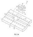
- FIG. 3A is a chip resistor with a single outrigger prior to assembly according to an implementation of the present disclosure
- FIG. 3B is a chip resistor with a single outrigger after assembly according to an implementation of the present disclosure
- FIG. 4A is a chip resistor with double outriggers prior to assembly according to an implementation of the present disclosure
- FIG. 4B is a chip resistor with double outriggers after assembly according to an implementation of the present disclosure
- FIG. 5 is a graph of performance data according to an implementation of the present disclosure.
- FIG. 6 is a table of performance data according to an implementation of the present disclosure.
- FIG. 7 is a table of specifications according to an implementation of the present disclosure.
- FIG. 8 is a table of materials according to an implementation of the present disclosure.
- the drawings show a chip resistor which has an industry-standard footprint but with improved power handling capability while maintaining very low capacitance and inductance.
- a typical, commercially available, surface mount resistor in the 0402 size has a power rating of about 0.063 watts.
- the chip resistor described herein has a power rating of 1 watt, more than 15 times greater than currently available products, while maintaining the same footprint and low capacitance and inductance.
- the 0402 size is used here as an example, the concept is scalable to larger and smaller size chips.
- the frequencies discussed by the present disclosure range from about 100 KHz to 60 GHz or any portion thereof. However, in other implementations, other frequencies may be utilized.
- FIG. 1 presents a chip resistor 100 according to an implementation of the present disclosure.
- the chip resistor 100 includes a substrate 110 .
- a resistor element 140 and two contacts 130 lie on a top surface of a main portion 112 of the substrate 110 .
- a ground plane attachment area 120 lies on a top surface of an extended portion 114 of the substrate 110 .
- the substrate 110 may be made of a ceramic material.
- the resistor element 140 , the contacts 130 , and the ground plane attachment area 120 may be screen printed or otherwise deposited onto the substrate 110 .
- the resistor element 140 may be formed using a resistive ink or a conductive ink in screen and stencil printing processes, sometimes referred to as “thick film” resistors, which generally have a thickness between about 200 micro-inches to about 1000 micro-inches.
- the resistor element 140 can be formed using sputtering, evaporation or other vacuum deposition processes of a resistive material and etched, sometimes referred to as “thin film” resistors, which generally have a thickness between about 300 Angstroms to 25,500 Angstroms (1.2 micro-inches to 100.4 micro-inches).
- the chip resistor 100 exhibits improved thermal performance by utilizing ground plane material that is already available on a printed circuit board (PCB).
- Ground planes are generally made of copper, which is an excellent heat conductor. Ground planes are also highly solderable which facilitates attachment of components.
- the ground plane material provides for the correct functioning of microwave circuits and is necessary for optimal circuit operation, but is generally unused to attach other components.
- the chip resistor 100 incorporates the addition of an extended piece of ceramic material, the extended portion 114 , attached to the resistor substrate, the main portion 112 , which is then soldered down to the existing ground plane on the circuit board. Heat is drawn away from the resistor element 140 , where the heat is generated, and dissipating it safely into the surrounding metal ground plane.
- the chip resistor 100 has one “outrigger,” or extra piece of ceramic material (i.e. the extended portion 114 ) attached for applications having only one available ground plane. As will be discussed below, other implementations may have more outriggers.
- the additional piece of ceramic, the extended portion 114 has minimal or no effect on the response of the circuit, thus retuning is not necessary.
- Adding the additional piece of ceramic adds almost no cost to the manufacturing of the chip resistor 100 , but results in considerably higher performance, mechanically, thermally, and electrically.
- FIGS. 2A and 2B illustrate exemplary dimensions for manufacturing chip resistors similar to the chip resistor 100 .
- the dimensions and thicknesses may vary based on the application.
- a chip resistor 200 in FIG. 2A may be similar to the chip resistor 100 .
- the chip resistor 200 has contacts 230 , a resistor element 240 , and a ground plane attachment area 220 over a substrate 210 .
- the substrate 210 has a width 216 , which may be about 0.040 inches, and a height 214 , which may be about 0.060 inches.
- Each contact 230 has a width 232 , which may be about 0.010 inches, and a height 234 , which may be about 0.020 inches.
- Each contact 230 is a distance 212 , which may be about 0.005 inches, offset from an edge of the substrate 210 , while aligned against side edges of the substrate 210 , as seen in FIG. 2A .
- the resistor element 240 is between and touches the contacts 230 .
- the resistor element 240 has a height 242 , which may be about 0.010 inches, and a width 244 , which may be about 0.020 inches. Note that the widths 232 and 244 approximately equal the width 216 .
- the ground plane attachment area 220 also has the width 216 .
- the ground plane attachment area 220 also has a height 222 , which may be about 0.0
- FIG. 2B depicts a wafer 250 having an array of chip resistors 200 .
- the wafer 250 has a width 252 , which may be about 3.000 inches, and a height 256 , which may be about 3.000 inches.
- the wafer 250 is a 3 inch square wafer, but in other implementations the dimensions may vary as needed.
- the wafer 250 may hold an array of 40 ⁇ 30 chip resistors 200 , although in other implementations the size of the array may vary.
- the array is offset a distance 254 , which may be about 0.505 inches, from a side edge of the wafer 250 , and offset a distance 258 , which may be about 0.455 inches, from a top edge of the wafer 250 , as seen in FIG. 2B .
- the chip resistors 200 further include a protective coating 245 covering the resistor element 240 .
- the protective coating 245 shares the width 244 of the resistor element 240 , and the height 234 of the contacts 230 .
- each chip resistor 200 is spaced a distance 264 , which may be about 0.010 inches, from neighboring chip resistors 200 in the same row, and spaced a distance 262 , which may be about 0.010 inches, from adjacent rows.
- multiple chip resistors 200 may be fabricated on a single wafer 250 .
- FIG. 3A depicts a pre-assembled state 300 of a chip resistor 305 .
- the chip resistor 305 may be similar to the chip resistors 100 and 200 .
- the chip resistor 305 includes a substrate 310 which includes a main portion 312 and an outrigger 314 , a ground plane attachment area 320 , an input contact 330 , an output contact 335 , and a resistor element 340 .
- the chip resistor 305 is configured to attach to a coplanar wave guide structure 350 .
- the coplanar wave guide structure 350 includes RF traces 360 , and via holes 370 , which connect to a bottom ground plane not seen in FIG. 3A .
- a heat sink area 315 corresponds to an attachment area for the chip resistor 305 .
- the input contact 330 aligns with and contacts the RF trace 360
- the output contact 335 aligns with and contacts the other RF trace 360 .
- the ground plane attachment area 320 aligns with and contacts several via holes 370 for connection to the ground plane.
- An assembled state 302 is depicted in FIG. 3B .
- Another implementation may incorporate two outriggers, rather than one. With two outriggers, the resistor element is mounted centrally between two thermal paths to the ground plane. Two outriggers advantageously doubles the power handling capability of the chip resistor and works particularly well for RF circuits using Coplanar Ground Planes (CPWs), where there is copper material already available on both sides of the RF transmission line, resulting in a very efficient heat sink.
- CPWs Coplanar Ground Planes
- FIGS. 4A and 4B show a double outrigger arrangement according to an implementation of the present disclosure.
- FIG. 4A illustrates a pre-assembled state 400 of a chip resistor 405 .
- the chip resistor 405 includes a substrate 410 which includes a main portion 412 .
- the chip resistor 405 also includes an input contact 430 , an output contact 435 , and a resistor element 440 .
- the chip resistor 405 includes a first extended portion or outrigger 414 and a second extended portion or outrigger 416 .
- the chip resistor 405 further includes a first ground plane attachment area 420 over the first extended portion 414 and a second ground plane attachment area 425 over the second extended portion 416 .
- the chip resistor 405 is configured to attach to a coplanar wave guide structure 450 , which may be similar to the coplanar wave guide structure 350 .
- the coplanar wave guide structure 450 includes RF traces 460 , and via holes 470 , which may connect to a bottom ground plane not seen in FIG. 4A .
- a heat sink area 415 corresponds to an attachment area for the chip resistor 405 . As compared to the heat sink area 315 in FIG. 3A , the heat sink area 415 is larger, encompassing two rows of via holes 470 rather than just one.
- the input contact 430 aligns with and contacts the RF trace 460
- the output contact 435 aligns with and contacts the other RF trace 460
- the ground plane attachment area 420 aligns with and contacts a first row of via holes 470 for connection to the ground plane.
- the ground plane attachment area 425 aligns with and contacts a second row of via holes 470 for connection to the ground plane.
- An assembled state 402 is depicted in FIG. 4B .
- FIG. 5 shows a graph 500 of performance results of a chip resistor, such as the chip resistor 100 , 200 , 305 , or 405 , listed in table 600 of FIG. 6 .
- a chip resistor such as the chip resistor 100 , 200 , 305 , or 405 , listed in table 600 of FIG. 6 .
- the temperature rises.
- the chip resistor of the present disclosure reaches a temperature of about 75.1 degrees C. at 1 watt, which generally outperforms conventional chip resistors.
- FIG. 7 presents a table 700 of typical specifications of a chip resistor according to an implementation of the present disclosure.
- FIG. 8 presents a table 800 of exemplary materials for fabricating the chip resistor 200 , although in other implementations other suitable materials may be used.
- the substrate 210 may be made of alumina 96%, 15 mil thick.
- the contacts 230 may be made of conductor ink Ferro C4270 made of platinum/gold.
- the resistor element 240 may be made of DuPont resistor ink at 50 ohms/square for a 131 ohm resistor, or DuPont resistor ink at 100 ohms/square for a 262 ohm resistor.
- the protective coating 245 may be made of Ferro blue protective coating.
Landscapes
- Engineering & Computer Science (AREA)
- Microelectronics & Electronic Packaging (AREA)
- Physics & Mathematics (AREA)
- Thermal Sciences (AREA)
- Computer Networks & Wireless Communication (AREA)
- Signal Processing (AREA)
- Non-Adjustable Resistors (AREA)
Abstract
Description
Claims (20)
Priority Applications (1)
| Application Number | Priority Date | Filing Date | Title |
|---|---|---|---|
| US14/015,914 US8994490B2 (en) | 2012-08-30 | 2013-08-30 | Chip resistor with outrigger heat sink |
Applications Claiming Priority (2)
| Application Number | Priority Date | Filing Date | Title |
|---|---|---|---|
| US201261695193P | 2012-08-30 | 2012-08-30 | |
| US14/015,914 US8994490B2 (en) | 2012-08-30 | 2013-08-30 | Chip resistor with outrigger heat sink |
Publications (2)
| Publication Number | Publication Date |
|---|---|
| US20140060897A1 US20140060897A1 (en) | 2014-03-06 |
| US8994490B2 true US8994490B2 (en) | 2015-03-31 |
Family
ID=50184452
Family Applications (1)
| Application Number | Title | Priority Date | Filing Date |
|---|---|---|---|
| US14/015,914 Active 2033-11-23 US8994490B2 (en) | 2012-08-30 | 2013-08-30 | Chip resistor with outrigger heat sink |
Country Status (2)
| Country | Link |
|---|---|
| US (1) | US8994490B2 (en) |
| WO (1) | WO2014036486A1 (en) |
Cited By (1)
| Publication number | Priority date | Publication date | Assignee | Title |
|---|---|---|---|---|
| US11967609B2 (en) | 2018-06-06 | 2024-04-23 | KYOCERA AVX Components Corporation | High frequency and high power thin-film component |
Citations (12)
| Publication number | Priority date | Publication date | Assignee | Title |
|---|---|---|---|---|
| US5179366A (en) | 1991-06-24 | 1993-01-12 | Motorola, Inc. | End terminated high power chip resistor assembly |
| JPH08222401A (en) | 1995-02-14 | 1996-08-30 | Toshiba Corp | High frequency circuit device |
| US5841340A (en) * | 1996-05-07 | 1998-11-24 | Rf Power Components, Inc. | Solderless RF power film resistors and terminations |
| US5945905A (en) * | 1998-12-21 | 1999-08-31 | Emc Technology Llc | High power resistor |
| US20040198100A1 (en) | 2003-04-01 | 2004-10-07 | Fink Randy L. | High voltage electrical connection |
| US7190252B2 (en) * | 2005-02-25 | 2007-03-13 | Vishay Dale Electronics, Inc. | Surface mount electrical resistor with thermally conductive, electrically insulative filler and method for using same |
| KR20090105058A (en) | 2008-04-01 | 2009-10-07 | 엘에스전선 주식회사 | Shielded connector and shielded connector set with the same |
| US20100328021A1 (en) | 2007-06-29 | 2010-12-30 | Koa Corporation | Resistor device |
| KR20110073765A (en) | 2009-12-24 | 2011-06-30 | 삼성전기주식회사 | Chip resister and method of manufacturing the same |
| US20110156860A1 (en) | 2009-12-28 | 2011-06-30 | Vishay Dale Electronics, Inc. | Surface mount resistor with terminals for high-power dissipation and method for making same |
| US8043106B1 (en) | 2010-03-30 | 2011-10-25 | Delphi Technologies, Inc. | Low profile socket connector with flexing lock arm |
| US8823483B2 (en) * | 2012-12-21 | 2014-09-02 | Vishay Dale Electronics, Inc. | Power resistor with integrated heat spreader |
-
2013
- 2013-08-30 US US14/015,914 patent/US8994490B2/en active Active
- 2013-08-30 WO PCT/US2013/057665 patent/WO2014036486A1/en active Application Filing
Patent Citations (12)
| Publication number | Priority date | Publication date | Assignee | Title |
|---|---|---|---|---|
| US5179366A (en) | 1991-06-24 | 1993-01-12 | Motorola, Inc. | End terminated high power chip resistor assembly |
| JPH08222401A (en) | 1995-02-14 | 1996-08-30 | Toshiba Corp | High frequency circuit device |
| US5841340A (en) * | 1996-05-07 | 1998-11-24 | Rf Power Components, Inc. | Solderless RF power film resistors and terminations |
| US5945905A (en) * | 1998-12-21 | 1999-08-31 | Emc Technology Llc | High power resistor |
| US20040198100A1 (en) | 2003-04-01 | 2004-10-07 | Fink Randy L. | High voltage electrical connection |
| US7190252B2 (en) * | 2005-02-25 | 2007-03-13 | Vishay Dale Electronics, Inc. | Surface mount electrical resistor with thermally conductive, electrically insulative filler and method for using same |
| US20100328021A1 (en) | 2007-06-29 | 2010-12-30 | Koa Corporation | Resistor device |
| KR20090105058A (en) | 2008-04-01 | 2009-10-07 | 엘에스전선 주식회사 | Shielded connector and shielded connector set with the same |
| KR20110073765A (en) | 2009-12-24 | 2011-06-30 | 삼성전기주식회사 | Chip resister and method of manufacturing the same |
| US20110156860A1 (en) | 2009-12-28 | 2011-06-30 | Vishay Dale Electronics, Inc. | Surface mount resistor with terminals for high-power dissipation and method for making same |
| US8043106B1 (en) | 2010-03-30 | 2011-10-25 | Delphi Technologies, Inc. | Low profile socket connector with flexing lock arm |
| US8823483B2 (en) * | 2012-12-21 | 2014-09-02 | Vishay Dale Electronics, Inc. | Power resistor with integrated heat spreader |
Cited By (1)
| Publication number | Priority date | Publication date | Assignee | Title |
|---|---|---|---|---|
| US11967609B2 (en) | 2018-06-06 | 2024-04-23 | KYOCERA AVX Components Corporation | High frequency and high power thin-film component |
Also Published As
| Publication number | Publication date |
|---|---|
| WO2014036486A1 (en) | 2014-03-06 |
| US20140060897A1 (en) | 2014-03-06 |
Similar Documents
| Publication | Publication Date | Title |
|---|---|---|
| CN109417054B (en) | Ceramic substrate for high frequency and semiconductor element housing package for high frequency | |
| EP3327767B1 (en) | Mount structure, method of manufacturing mount structure, and wireless device | |
| US20080003846A1 (en) | Circuit board unit | |
| WO2018021209A1 (en) | Substrate for mounting semiconductor element and semiconductor device | |
| US11310904B2 (en) | Chip package and power module | |
| JP4882974B2 (en) | High frequency module | |
| US10204721B2 (en) | Resistor element and method of manufacturing the same | |
| JP2018129596A (en) | Wireless device | |
| US8994490B2 (en) | Chip resistor with outrigger heat sink | |
| JP4203499B2 (en) | Chip resistor and manufacturing method of chip resistor | |
| EP0912997A1 (en) | Rf power package with a dual ground | |
| EP2907191B1 (en) | Radiofrequency absorptive filter | |
| US9668348B2 (en) | Multi-terminal electronic component, method of manufacturing the same, and board having the same | |
| JP5525875B2 (en) | Optical module | |
| WO2021192766A1 (en) | Communication device | |
| US20060002092A1 (en) | Board mounted heat sink using edge plating | |
| KR102229555B1 (en) | Integral spring loaded chip termination | |
| KR20220074939A (en) | Systems and Processes for Increasing Semiconductor Device Reliability | |
| JP4685660B2 (en) | Wiring structure of semiconductor parts | |
| JPWO2020095733A1 (en) | Resistor | |
| US9824798B2 (en) | Resistor element and method of manufacturing the same | |
| JP5821750B2 (en) | Antenna device | |
| JP7005111B2 (en) | Electronic component mounting product | |
| JP2004241944A (en) | Irreversible circuit element, mounting structure for irreversible circuit element, and communication device | |
| JP2022049344A (en) | Optical semiconductor device |
Legal Events
| Date | Code | Title | Description |
|---|---|---|---|
| AS | Assignment |
Owner name: SMITHS INTERCONNECT MICROWAVE COMPONENTS, INC., FL Free format text: ASSIGNMENT OF ASSIGNORS INTEREST;ASSIGNORS:DAVIDSSON, PAUL;BLACKA, ROBERT;LOH, KAI;REEL/FRAME:031121/0815 Effective date: 20130830 |
|
| STCF | Information on status: patent grant |
Free format text: PATENTED CASE |
|
| MAFP | Maintenance fee payment |
Free format text: PAYMENT OF MAINTENANCE FEE, 4TH YEAR, LARGE ENTITY (ORIGINAL EVENT CODE: M1551); ENTITY STATUS OF PATENT OWNER: LARGE ENTITY Year of fee payment: 4 |
|
| AS | Assignment |
Owner name: INTERCONNECT DEVICES, INC., DELAWARE Free format text: MERGER;ASSIGNOR:SMITHS INTERCONNECT MICROWAVE COMPONENTS, INC.;REEL/FRAME:048682/0201 Effective date: 20170731 Owner name: SMITHS INTERCONNECT AMERICAS, INC., DELAWARE Free format text: CHANGE OF NAME;ASSIGNOR:INTERCONNECT DEVICES, INC.;REEL/FRAME:048682/0212 Effective date: 20170731 |
|
| MAFP | Maintenance fee payment |
Free format text: PAYMENT OF MAINTENANCE FEE, 8TH YEAR, LARGE ENTITY (ORIGINAL EVENT CODE: M1552); ENTITY STATUS OF PATENT OWNER: LARGE ENTITY Year of fee payment: 8 |