US8990760B2 - Cell-aware fault model generation for delay faults - Google Patents
Cell-aware fault model generation for delay faults Download PDFInfo
- Publication number
- US8990760B2 US8990760B2 US13/219,564 US201113219564A US8990760B2 US 8990760 B2 US8990760 B2 US 8990760B2 US 201113219564 A US201113219564 A US 201113219564A US 8990760 B2 US8990760 B2 US 8990760B2
- Authority
- US
- United States
- Prior art keywords
- cycle
- defects
- type
- detectable
- cell
- Prior art date
- Legal status (The legal status is an assumption and is not a legal conclusion. Google has not performed a legal analysis and makes no representation as to the accuracy of the status listed.)
- Active, expires
Links
Images


Classifications
-
- G—PHYSICS
- G01—MEASURING; TESTING
- G01R—MEASURING ELECTRIC VARIABLES; MEASURING MAGNETIC VARIABLES
- G01R31/00—Arrangements for testing electric properties; Arrangements for locating electric faults; Arrangements for electrical testing characterised by what is being tested not provided for elsewhere
- G01R31/28—Testing of electronic circuits, e.g. by signal tracer
- G01R31/317—Testing of digital circuits
- G01R31/3181—Functional testing
- G01R31/3183—Generation of test inputs, e.g. test vectors, patterns or sequences
- G01R31/318342—Generation of test inputs, e.g. test vectors, patterns or sequences by preliminary fault modelling, e.g. analysis, simulation
- G01R31/31835—Analysis of test coverage or failure detectability
-
- G06F17/5036—
-
- G—PHYSICS
- G06—COMPUTING; CALCULATING OR COUNTING
- G06F—ELECTRIC DIGITAL DATA PROCESSING
- G06F30/00—Computer-aided design [CAD]
- G06F30/30—Circuit design
- G06F30/36—Circuit design at the analogue level
- G06F30/367—Design verification, e.g. using simulation, simulation program with integrated circuit emphasis [SPICE], direct methods or relaxation methods
Definitions
- the present invention is directed to testing of integrated circuits (ICs).
- ICs integrated circuits
- Various aspects of the invention may be particularly useful for modeling defects and generating high quality test patterns for delay Faults.
- a wide range of conventional fault models have been used by automated test pattern generation (ATPG) tools to generate test patterns for detecting defects in integrated circuits, such as stuck-at, bridging, inter-cell-opens, and transition faults. While the conventional fault models are efficient in addressing defects between library cell instances, at the ports of library cells, and between the interconnect lines outside of library cells, many intra-cell defects are not detectable by test patterns generated based on the conventional fault models.
- a wide range of conventional fault models have been used by automated test pattern generation (ATPG) tools to generate test patterns for detecting defects in integrated circuits, such as stuck-at, bridging, inter-cell-opens, and transition faults.
- N-detection based approaches improve the defect coverage by targeting the same fault multiple times under different conditions. However, this typically increases the number of patterns by a factor of N and therefore makes the testing costly.
- Embedded multi detect based approaches increase the defect coverage by utilizing unused bits in existing test patterns. Unlike the methods based on N-detection, no additional test patterns are needed with the EMD-based approaches. Nevertheless, there exists only a probabilistic relation to actual defects for both techniques. Thus, it is difficult to quantify the additional defect coverage provided by these techniques relative to conventional techniques, and to predict the resulting benefit for future designs.
- Gate-exhaustive testing approaches are also developed to detect intra-cell defects. Like the N-detection based approaches, however, the gate-exhaustive testing approaches tend to generate a very large number of additional patterns and result in high test costs.
- Cell-aware fault models have been developed to directly target intra-cell defects. The methods are discussed in U.S. patent application Ser. No. 12/718,799, entitled “Cell-Aware Fault Model Creation And Pattern Generation,” filed on Mar. 5, 2010, and naming Friedrich Hapke et al. as inventors, which application is incorporated entirely herein by reference (referred to as “U.S. patent application Ser. No. '799” hereinafter).
- intra-cell defects are extracted based on both layout data and transistor-level netlists for a library cells. Analog simulations are applied to determine detection conditions for the defects.
- the cell-aware based approaches can be applied to various intra-cell defects that can cause stuck-at and time-related faults. For many time-related faults, two-cycle sequential testing is needed. Due to exhaustive simulations in two time frames, however, generation of timing-related cell-aware fault models can lead to long analog fault simulation runtimes.
- cell-aware fault models for a library cell are created based on a transistor-level netlist of the cell and defects of interest determined based on the layout data and the transistor-level netlist.
- analog one-clock-cycle (or one-cycle) fault simulations are first performed for the defects of interest to identify type one detectable defects and type two detectable defects.
- the type one detectable defects are detectable by one-cycle testing and their fault models may be created based on results of the analog one-cycle fault simulations for the type one detectable defects.
- the type two detectable defects are defects for which two-cycle detection conditions may be calculated from corresponding results of the analog one-cycle fault simulations. Analog two-cycle fault simulations may then be performed for defects in the defects of interest that are neither type-one detectable defects nor type-two detectable defects to determine type three detectable defects and their two-cycle detection conditions. Finally, two-cycle cell-aware fault models for the type two and type three detectable defects may be created based on the corresponding two-cycle detection conditions. One-cycle cell aware fault models for the type one detectable defects may be determined based on results of the analog one-cycle fault simulations for the type one detectable defects. The created one-cycle and two-cycle cell-aware fault models can be used to generate test patterns.
- FIG. 1 illustrates a programmable computer system with which various embodiments of the invention may be employed.
- FIG. 2 illustrates an example of two-clock-cycle testing.
- FIG. 3 illustrates an example of a library cell with delay faults.
- FIG. 4 illustrates an example of a cell-aware fault model creation system according to various embodiments of the invention.
- any of the disclosed techniques can be implemented in whole or in part by software comprising computer-executable instructions stored on computer-readable media.
- Such software can comprise, for example, an appropriate electronic design automation (“EDA”) software tool (e.g., an automatic test pattern generation (“ATPG”) tool).
- EDA electronic design automation
- AVG automatic test pattern generation
- Such software can be executed on a single computer or on a networked computer (e.g., via the Internet, a wide-area network, a local-area network, a client-server network, or other such network).
- EDA electronic design automation
- AVG automatic test pattern generation
- Such software can be executed on a single computer or on a networked computer (e.g., via the Internet, a wide-area network, a local-area network, a client-server network, or other such network).
- a networked computer e.g., via the Internet, a wide-area network, a local-area network, a client-server network, or other such network.
- the disclosed technology can be implemented using any commercially available computer executing a program written in any commercially available or otherwise suitable language. Any of the disclosed methods can alternatively be implemented (partially or completely) in hardware (e.g., an ASIC, PLD, or SoC).
- Any data produced from any of the disclosed methods can be stored on computer-readable media (e.g., tangible computer-readable media, such as one or more CDs, volatile memory components (such as DRAM or SRAM), or nonvolatile memory components (such as hard drives)) using a variety of different data structures or formats.
- computer-readable media e.g., tangible computer-readable media, such as one or more CDs, volatile memory components (such as DRAM or SRAM), or nonvolatile memory components (such as hard drives)
- Such data can be created, updated, or stored using a local computer or over a network (e.g., by a server computer).
- the singular forms “a,” “an,” and “the” include the plural forms unless the context clearly dictates otherwise. Additionally, the term “includes” means “comprises.” Moreover, unless the context dictates otherwise, the term “coupled” means electrically or electromagnetically connected or linked and includes both direct connections or direct links and indirect connections or indirect links through one or more intermediate elements not affecting the intended operation of the circuit. Furthermore, the term “design” is intended to encompass data describing an entire microdevice, such as an integrated circuit device or micro-electromechanical system (MEMS) device.
- MEMS micro-electromechanical system
- This term also is intended to encompass a smaller group of data describing one or more components of an entire microdevice, however, such as a layer of an integrated circuit device, or even a portion of a layer of an integrated circuit device.
- the term “design” also is intended to encompass data describing more than one microdevice, such as data to be used to create a mask or reticle for simultaneously forming multiple microdevices on a single wafer.
- the layout design data may be in any desired format, such as, for example, the Graphic Data System II (GDSII) data format or the Open Artwork System Interchange Standard (OASIS) data format proposed by Semiconductor Equipment and Materials International (SEMI).
- GDSII Graphic Data System II
- OASIS Open Artwork System Interchange Standard
- Other formats include an open source format named Open Access, Milkyway by Synopsys, Inc., and EDDM by Mentor Graphics, Inc.
- FIG. 1 shows an illustrative example of a computing device 101 .
- the computing device 101 includes a computing unit 103 with a processing unit 105 and a system memory 107 .
- the processing unit 105 may be any type of programmable electronic device for executing software instructions, but will conventionally be a microprocessor.
- the system memory 107 may include both a read-only memory (ROM) 109 and a random access memory (RAM) 111 .
- ROM read-only memory
- RAM random access memory
- both the read-only memory (ROM) 109 and the random access memory (RAM) 111 may store software instructions for execution by the processing unit 105 .
- the processing unit 105 and the system memory 107 are connected, either directly or indirectly, through a bus 113 or alternate communication structure, to one or more peripheral devices.
- the processing unit 105 or the system memory 107 may be directly or indirectly connected to one or more additional memory storage devices, such as a “hard” magnetic disk drive 115 , a removable magnetic disk drive 117 , an optical disk drive 119 , or a flash memory card 121 .
- the processing unit 105 and the system memory 107 also may be directly or indirectly connected to one or more input devices 123 and one or more output devices 125 .
- the input devices 123 may include, for example, a keyboard, a pointing device (such as a mouse, touchpad, stylus, trackball, or joystick), a scanner, a camera, and a microphone.
- the output devices 125 may include, for example, a monitor display, a printer and speakers.
- one or more of the peripheral devices 115 - 125 may be internally housed with the computing unit 103 .
- one or more of the peripheral devices 115 - 125 may be external to the housing for the computing unit 103 and connected to the bus 113 through, for example, a Universal Serial Bus (USB) connection.
- USB Universal Serial Bus
- the computing unit 103 may be directly or indirectly connected to one or more network interfaces 127 for communicating with other devices making up a network.
- the network interface 127 translates data and control signals from the computing unit 103 into network messages according to one or more communication protocols, such as the transmission control protocol (TCP) and the Internet protocol (IP).
- TCP transmission control protocol
- IP Internet protocol
- the interface 127 may employ any suitable connection agent (or combination of agents) for connecting to a network, including, for example, a wireless transceiver, a modem, or an Ethernet connection.
- TCP transmission control protocol
- IP Internet protocol
- connection agent or combination of agents
- the computer 101 is illustrated as an example only, and it not intended to be limiting.
- Various embodiments of the invention may be implemented using one or more computing devices that include the components of the computer 101 illustrated in FIG. 1 , which include only a subset of the components illustrated in FIG. 1 , or which include an alternate combination of components, including components that are not shown in FIG. 1 .
- various embodiments of the invention may be implemented using a multi-processor computer, a plurality of single and/or multiprocessor computers arranged into a network, or some combination of both.
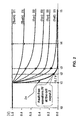
- FIG. 2 illustrates an example of the two-cycle testing.
- Waveform D 4 represents a fault-free waveform.
- the two-cycle testing applies a stimulus to the inputs of the circuit under test to establish a value at an output.
- the established output value is 1.0 volt.
- t 1 the onset of the second clock cycle
- another stimulus is applied to the inputs of the circuit to induce a transition at the output.
- the output value drops to 0.1 volt at t 2 and settle to 0 volt at t 4 .
- Different types of defects can cause the output value to settle at different values.
- Waveforms D 1 represent a type of defects (D 1 defects or type one defects) that can be detected by probing the output voltage at as late as t 5 , i.e., when the circuit reaches a steady state.
- the two-cycle testing for D 2 is sometimes referred to as gross delay testing.
- One-clock-cycle testing (or one-cycle testing) can also be applied to detect the D 1 defects because the value at the output never drops below a threshold voltage and can be treated as settling at a state opposite to that in the defect-free case.
- FIG. 3 illustrates an example of a library cell.
- a D 1 defect may be a bridge to ground at location 310 . This bridge influences both P-type and N-type transistors.
- Waveforms D 2 represent a type of defects (D 2 defects or type two defects) that can be detected by probing the output voltage not at t 5 but at an earlier time such as t 3 because the steady-state values (at t 5 ) for the output lie, e.g., between 0.2 and 0.8 volts which are below the threshold voltage.
- the two-clock-cycle testing for D 2 is sometimes referred to as small delay testing, in contrast to the gross delay testing for detecting the D 1 defects.
- a D 2 defect may be a bridge to ground at location 320 . This bridge causes one of the parallel transistors (M 15 ) to be switched on when it should be switched off. Thus, some P-type and N-type transistors are switched on at the same time and produce a longer delay than the defect-free circuit but shorter delay than the circuit with a D 1 defect.
- Waveform D 3 represents a type of defects (D 3 defects or type three defects) that can also be detected by the small delay testing but at an even earlier time. Unlike the D 1 and D 2 defects, the D 3 defects do not produce a steady state voltage of the output different from that for the defect-free circuit. In FIG. 2 , for example, the steady state voltage for the D 3 defects drops to 0 volt.
- a D 3 defect may be a bridge to Vdd at location 330 . This bridge switches off one of the parallel transistors (M 18 ) when it should be switched on.
- the D 3 defects may be considered to be detected when the voltage of the output deviates more than a specified limit from the defect-free case at a certain time after t j .
- the D 3 defects may also be detected by measuring the delayed transition time.
- N 2(robust) 2 m ⁇ m ⁇ ( d+ 1).
- N 2(non-robust) 2 m ⁇ (2 m -1) ⁇ ( d+ 1).
- N 1 2 m ⁇ ( d+ 1).
- m denote the number of inputs of a library cell
- d denotes the number of defects considered
- the operand “+1” correlates to a fault-free simulation.
- the number of library cell inputs is typically in the range of 1 to 8, while the number of defects could easily reach a few hundreds. Comparing the three equations, it is easy to understand why it is desirable to reduce the number of defects that need to be simulated with the analog two-cycle simulations.
- analog one-cycle simulations may be used to identify the D 1 and D 2 defects in defects of interest due to the fact that the steady state values for the output caused by D 1 and D 2 are different from that in the defect-free case.
- the D 1 defects can be detected under the one-cycle testing.
- the detection conditions for the D 1 defects can be readily obtained from the analog one-cycle simulations.
- the D 2 defects are not detectable under the one-cycle testing.
- the detection conditions for the D 2 defects can still be derived from the one-clock-cycle simulations, which will be discussed in detail below.
- the D 3 defects are the only ones that need analog two-cycle simulations.
- FIG. 4 illustrates an example of a tool for generating cell-aware fault models and test patterns according to various embodiments of the invention.
- the tool has two main systems: a cell-aware fault model creation system 400 and a cell-aware pattern generation system 480 .
- the cell-aware fault model creation system 400 creates fault models for a cell of a library based on the cell's layout data and transistor-level netlist.
- the created cell-aware fault models may be stored in a cell-aware fault model database 475 .
- the cell-aware pattern generation system 480 may then use the created fault models to generate test patterns, which may be stored in a test pattern database 485 .
- the cell-aware fault model creation system 400 may include, as shown in FIG. 4 , four units: an analog one-cycle simulation unit 440 , a two-cycle calculation unit 450 , an analog two-cycle simulation unit 460 and a fault model synthesis unit 470 . As will be discussed in more detail below, some implementations of the cell-aware fault model creation system 400 may cooperate with (or incorporated) one or more of a layout database 405 , a netlist extraction unit 410 , a transistor-level netlist database 415 , a defect extraction unit 420 , and a defects of interest database 425 .
- one or some of the netlist extraction unit 410 , the defect extraction unit 420 , the analog one-cycle simulation unit 440 , the two-cycle calculation unit 450 , the analog two-cycle simulation unit 460 , the fault model synthesis unit 470 , and the cell-aware pattern generation system 480 may be implemented by one or more computing systems, such as the computing system illustrated in FIG. 1 , executing programmable instructions.
- some other embodiments of the invention may be implemented by software-executable instructions, stored on a computer-readable medium, for instructing a computing system to perform functions of one or some of the netlist extraction unit 410 , the defect extraction unit 420 , the analog one-cycle simulation unit 440 , the two-cycle calculation unit 450 , the analog two-cycle simulation unit 460 , the fault model synthesis unit 470 , and the cell-aware pattern generation system 480 .
- the computer-readable medium may be, for example, a magnetic storage device, an optical storage device, a “punched” surface type device, or a solid state storage device.
- the layout database 405 While the layout database 405 , the transistor-level netlist database 415 , the defects of interest database 425 , the cell-aware fault model database 475 , and the test pattern database 485 are shown as separate units in FIG. 4 , a single computer-readable medium may be used to implement some or all of these databases.
- cell-aware fault model generation methods that may be employed according to various embodiments of the invention will be described with reference to the tool for generating cell-aware fault models and test patterns illustrated in FIG. 4 . It should be appreciated, however, that alternate implementations of a tool for generating cell-aware fault models and test patterns may be used to perform the cell-aware fault model generation methods according to various embodiments of the invention. Likewise, the tool for generating cell-aware fault models and test patterns illustrated in FIG. 4 may be employed to perform other cell-aware fault model generation methods according to various embodiments of the invention.
- the analog one-cycle simulation unit 440 is configured to perform analog one-cycle fault simulations based on a transistor-level netlist of a library cell (or cell) to identify type one (D 1 ) detectable defects and type two (D 2 ) detectable defects in defects of interest.
- the transistor-level netlist may be extracted from layout data for the cell by the netlist extraction unit 410 .
- Various conventional tools can be employed by the netlist extraction unit 410 , such as the CALIBRE® Layout-Versus-Schematic (LVS) tool provided with the CALIBRE® family of physical verification software tool available from Mentor Graphics Corporation of Wilsonville, Oreg.
- the netlist extraction unit 410 may store the extracted transistor-level netlist in the transistor-level netlist database 415 for subsequent operations.
- the defects of interest may be determined by the defect extraction unit 420 based on the layout data and the transistor-level netlist.
- Various conventional tools may be used for the extraction process, such as the CALIBRE® xRCTM parasitic extraction tool provided with the CALIBRE® family of physical verification software tool available from Mentor Graphics Corporation of Wilsonville, Oreg.
- the extracted defects of interest may be stored in the defects of interest database 425 . It should be appreciated that the transistor-level netlist, the defects of interest, or both may be (alternatively or additionally) obtained in other ways. For example, users may provide some or all of the defects of interest based on their needs or experience.
- the defect extraction unit 420 may provide the defects of interest as parasitic features associated with a collection of geometric elements or location data for geometric elements in the layout design. Moreover, because the netlist extraction unit 410 produces the transistor-level netlist from the layout data, the components in the netlist can be correlated with the geometric elements in the layout design. In this manner, the position of the defects of interest relative to the components in the transistor-level netlist can be determined, and the defects can later be inserted (or “injected”) into the transistor-level netlist.
- the analog one-cycle simulation unit 440 may start the analog one-cycle simulations with netlist modification—defect injection. For example, if a bridge is a defect candidate, then a resistor may be inserted between the corresponding two nets. For an open fault, the corresponding electrical object (e.g. transistor gate, resistor, capacitor or the wire) is disconnected (or a very high resistance is included) during the analog simulations.
- netlist modification—defect injection For example, if a bridge is a defect candidate, then a resistor may be inserted between the corresponding two nets.
- the corresponding electrical object e.g. transistor gate, resistor, capacitor or the wire
- an exhaustive set of digital input patterns may be simulated on the modified netlist according to some embodiments of the invention. Additionally, each cell may be simulated without defects in order to determine the golden voltage (i.e., the expected voltage) at the cell outputs for every cell-input combination.
- the simulations are analog DC-analysis simulations (i.e., analog one-cycle simulations) which can determine the steady state voltage of the cell output(s).
- the analog one-cycle simulation unit 440 may determine whether a defect as a type one detectable defect, a type two detectable defect or a defect undetectable under the one-cycle testing.
- a type one detectable defect may be defined as the one that after being inserted, at least for one input combination (or assignment), one or more of the cell's output ports produce a voltage which is inverted to the golden voltage—e.g., the produced defective voltage deviates by 20% of the supply voltage from the fault free/golden output value.
- a type two detectable defect may be defined as the one that after being inserted, at least for one input combination (or assignment), one or more of the cell's output ports produce a voltage which deviates, e.g., by 20% to 80% of the supply voltage from the fault free/golden output value.
- the deviation threshold may also be specified by users.
- the simulations may be automated by a set of scripts around a state-of-the-art analog simulator.
- the results of the analog one-cycle fault simulations for the type one detectable defects may be summarized into a one-cycle detection matrix for each of the library cells.
- the detection matrix' rows and columns refer to input combinations and defects, respectively.
- the two-cycle calculation unit 450 is configured to determine two-cycle detection conditions (calculated two-cycle detection conditions) for the type two detectable defects based on results of the analog one-cycle fault simulations for the type two detectable defects. As mentioned above, the type two detectable defects cannot be detected under the one-cycle testing.
- the two-cycle detection conditions for the type-two detectable defects can be calculated from the results of the analog one-cycle fault simulations.
- the two-cycle detection conditions for a defect comprise combinations of input assignments for two clock cycles and corresponding output transition(s) that can be used to detect the defect.
- the two-cycle calculation unit 450 may first determine input assignments for the second clock cycle (or final time frame stimuli). In the results of the analog one-cycle fault simulations, those input assignments that cause one or more of the cell's output ports to produce a voltage which deviates, e.g., by 20% to 80% of the supply voltage from the fault free/golden output value may be designated as the input assignments for the second clock cycle. Based on the input assignments for the second clock cycle, the two-cycle calculation unit 450 may derive input assignments for the first clock cycle (or initial time frame stimuli) to form robust sequential testing. This may be done by inverting the value at one input of the final input assignment at a time.
- the calculated two-cycle detection conditions are derived by determining whether an edge at the output(s) is generated by a combination of one input assignment for the first clock cycle and one input assignment for the second clock cycle.
- An example of a robust two-cycle stimuli analysis is illustrated in Table 1.
- the column IT in Table 1 lists the stimuli to be applied during the initial timeframe.
- the column FT shows the stimuli to be applied during the final timeframe.
- the column Z contains the fault free waveform at the output of the cell.
- non-robust two-cycle stimuli When no robust two-cycle stimuli can produce an edge, non-robust two-cycle stimuli may be determined. To search for the non-robust two-cycle stimuli, more than one cell inputs may be inverted from the first clock cycle to the second clock cycle. The calculated two-cycle detection conditions for the type two detectable defects may be summarized into a two-cycle detection matrix for each of the library cells.
- the analog two-cycle simulation unit 460 is configured to perform analog two-cycle fault simulations to determine type three detectable defects and two-cycle detection conditions (simulated two-cycle detection conditions) for the type three detectable defects.
- the analog two-cycle fault simulations are performed only for those defects in the defects of interest that are neither the type one detectable defects nor the type two detectable defects.
- the analog two-cycle simulation unit 460 in some embodiments of the invention may construct robust two-cycle input assignments first to determine whether a defect is a type three detectable defect. When no robust two-cycle assignments can detect a defect, non-robust two-cycle assignments are used for the defect.
- the simulated two-cycle detection conditions for the type three detectable defects may be incorporated into the two-cycle detection matrix constructed by the two-cycle calculation unit 450 or summarized in a new two-cycle detection matrix for the type three detectable defects.
- the fault model synthesis unit 470 is configured to generate cell-aware fault models for two-cycle testing of the type two detectable defects and the type three detectable defects based on the calculated two-cycle detection conditions and the simulated two-cycle detection conditions.
- the fault model synthesis unit 470 may also generate cell-aware fault models for one-cycle testing of the type one detectable defects based on results of the analog one-cycle fault simulations for the type one detectable defects.
- the cell-aware fault models are sometimes also referred to as cell-aware library views. According to various embodiments of the invention, this synthesis operation extracts a set of necessary input assignments for each detectable defect to relax the future pattern generation process.
- the following method may be used for generating cell-aware fault models for one-cycle testing of the type one detectable defects.
- a detection matrix D is generated for an n-input library cell C implementing the combinational Boolean function F
- a detection function g d is generated based on the detection matrix D.
- This detection function g d incorporates all fully defined input-assignments which would be required to detect d, i.e. input assignments without don't-cares (or necessary input assignments).
- don't-cares may refer to input ports of a cell or bits in test patterns of which values are irrelevant to detecting defects of interest.
- every detection-function is combined with function F and its inverse F′ in order to find the corresponding output assignment for every cube contained in g d .
- all prime cubes of the resulting functions g dF and g dF′ are collected in the set R d .
- the method compresses identical cubes with respect to all sets R d and the corresponding defect information in two sets P and M, where P denotes the final set of primes cubes (the union of all prime cubes contained in all sets R d , d member of D), and M denotes a set of sets containing every detectable defect d detected by the corresponding prime cube.
- P denotes the final set of primes cubes (the union of all prime cubes contained in all sets R d , d member of D)
- M denotes a set of sets containing every detectable defect d detected by the corresponding prime cube.
- the mapping between an element of P and a set in M is defined via their
- the cell-aware pattern generation system 480 is configured to generate test patterns based on the created cell-aware fault models. Various methods such as those similar to what are described in the U.S. patent application Ser. No. '799 may be employed by the cell-aware pattern generation system 480 .
Landscapes
- Engineering & Computer Science (AREA)
- Computer Hardware Design (AREA)
- Physics & Mathematics (AREA)
- General Engineering & Computer Science (AREA)
- General Physics & Mathematics (AREA)
- Theoretical Computer Science (AREA)
- Microelectronics & Electronic Packaging (AREA)
- Evolutionary Computation (AREA)
- Geometry (AREA)
- Tests Of Electronic Circuits (AREA)
Abstract
Description
N 2(robust)=2m ·m·(d+1).
For non-robust sequential tests, the total number of analog simulations for a sequential analysis with two cycles (i.e. an initial and a final cycle) is:
N 2(non-robust)=2m·(2m-1)·(d+1).
On the other hand, the total number of analog simulations for a one-clock-cycle analysis is:
N 1=2m·(d+1).
| TABLE 1 |
| Robust two-cycle stimuli |
 |
Claims (26)
Priority Applications (1)
| Application Number | Priority Date | Filing Date | Title |
|---|---|---|---|
| US13/219,564 US8990760B2 (en) | 2011-08-26 | 2011-08-26 | Cell-aware fault model generation for delay faults |
Applications Claiming Priority (1)
| Application Number | Priority Date | Filing Date | Title |
|---|---|---|---|
| US13/219,564 US8990760B2 (en) | 2011-08-26 | 2011-08-26 | Cell-aware fault model generation for delay faults |
Publications (2)
| Publication Number | Publication Date |
|---|---|
| US20130054161A1 US20130054161A1 (en) | 2013-02-28 |
| US8990760B2 true US8990760B2 (en) | 2015-03-24 |
Family
ID=47744853
Family Applications (1)
| Application Number | Title | Priority Date | Filing Date |
|---|---|---|---|
| US13/219,564 Active 2033-06-01 US8990760B2 (en) | 2011-08-26 | 2011-08-26 | Cell-aware fault model generation for delay faults |
Country Status (1)
| Country | Link |
|---|---|
| US (1) | US8990760B2 (en) |
Cited By (2)
| Publication number | Priority date | Publication date | Assignee | Title |
|---|---|---|---|---|
| US10795751B2 (en) | 2017-03-03 | 2020-10-06 | Mentor Graphics Corporation | Cell-aware diagnostic pattern generation for logic diagnosis |
| US11994559B2 (en) | 2021-11-08 | 2024-05-28 | Texas Instruments Incorporated | Tests for integrated circuit (IC) chips |
Families Citing this family (13)
| Publication number | Priority date | Publication date | Assignee | Title |
|---|---|---|---|---|
| US9372946B2 (en) * | 2012-08-22 | 2016-06-21 | Mentor Graphics Corporation | Defect injection for transistor-level fault simulation |
| US8813004B1 (en) | 2012-11-21 | 2014-08-19 | Cadence Design Systems, Inc. | Analog fault visualization system and method for circuit designs |
| US8683400B1 (en) | 2012-11-21 | 2014-03-25 | Cadence Design Systems, Inc. | System and method for fault sensitivity analysis of mixed-signal integrated circuit designs |
| US8996348B1 (en) | 2012-11-21 | 2015-03-31 | Cadence Design Systems, Inc. | System and method for fault sensitivity analysis of digitally-calibrated-circuit designs |
| US8863050B1 (en) | 2013-03-15 | 2014-10-14 | Cadence Design Systems, Inc. | Efficient single-run method to determine analog fault coverage versus bridge resistance |
| US8875077B1 (en) * | 2014-02-10 | 2014-10-28 | Cadence Design Systems, Inc. | Fault sensitivity analysis-based cell-aware automated test pattern generation flow |
| WO2018026696A1 (en) * | 2016-07-31 | 2018-02-08 | Mentor Graphics Corporation | Activity coverage assessment of circuit designs under test stimuli |
| NL2023751B1 (en) * | 2019-09-03 | 2021-05-12 | Univ Delft Tech | Device Aware Test for Memory Units |
| TWI727478B (en) * | 2019-10-31 | 2021-05-11 | 瑞昱半導體股份有限公司 | Test pattern generating method and fault model generating method |
| CN112765928A (en) * | 2019-11-06 | 2021-05-07 | 瑞昱半导体股份有限公司 | Test pattern generation method and failure model generation method |
| US11182525B1 (en) * | 2020-07-07 | 2021-11-23 | Infineon Technologies Ag | Fault aware analog model (FAAM) |
| US11635462B2 (en) * | 2020-08-27 | 2023-04-25 | Siemens Industry Software Inc. | Library cell modeling for transistor-level test pattern generation |
| US11435401B1 (en) * | 2021-02-22 | 2022-09-06 | Cadence Design Systems, Inc. | Timed transition cell-aware ATPG using fault rule files and SDF for testing an IC chip |
Citations (14)
| Publication number | Priority date | Publication date | Assignee | Title |
|---|---|---|---|---|
| US5422891A (en) * | 1993-07-23 | 1995-06-06 | Rutgers University | Robust delay fault built-in self-testing method and apparatus |
| US5692160A (en) * | 1994-12-14 | 1997-11-25 | Vlsi Technology, Inc. | Temperature, process and voltage variant slew rate based power usage simulation and method |
| US6385750B1 (en) * | 1999-09-01 | 2002-05-07 | Synopsys, Inc. | Method and system for controlling test data volume in deterministic test pattern generation |
| US6832182B1 (en) * | 1999-04-08 | 2004-12-14 | Transim Technology Corporation | Circuit simulator |
| US7082559B2 (en) * | 2001-03-07 | 2006-07-25 | Kabushiki Kaisha Toshiba | Semiconductor integrated circuit device and test method thereof |
| US7137083B2 (en) * | 2004-04-01 | 2006-11-14 | Verigy Ipco | Verification of integrated circuit tests using test simulation and integrated circuit simulation with simulated failure |
| US20080141199A1 (en) * | 2006-12-07 | 2008-06-12 | Jens Bargfrede | Methods and apparatuses for timing analysis of electronics circuits |
| US20100109676A1 (en) * | 2007-04-12 | 2010-05-06 | Nxp, B.V. | Analog circuit testing and test pattern generation |
| US7747972B2 (en) * | 2006-12-07 | 2010-06-29 | Infineon Technologies Ag | Methods and apparatuses for timing analysis of electronic circuits |
| US20100229061A1 (en) | 2009-03-05 | 2010-09-09 | Friedrich Hapke | Cell-Aware Fault Model Creation And Pattern Generation |
| US20100293426A1 (en) * | 2009-05-13 | 2010-11-18 | Qualcomm Incorporated | Systems and methods for a phase locked loop built in self test |
| US8099269B2 (en) * | 2007-10-09 | 2012-01-17 | Globalfoundries Inc. | Two-step simulation methodology for aging simulations |
| US20130007684A1 (en) * | 2011-06-30 | 2013-01-03 | James Robert Kramer | Automated inline defect characterization |
| US8362622B2 (en) * | 2009-04-24 | 2013-01-29 | Synopsys, Inc. | Method and apparatus for placing transistors in proximity to through-silicon vias |
-
2011
- 2011-08-26 US US13/219,564 patent/US8990760B2/en active Active
Patent Citations (16)
| Publication number | Priority date | Publication date | Assignee | Title |
|---|---|---|---|---|
| US5422891A (en) * | 1993-07-23 | 1995-06-06 | Rutgers University | Robust delay fault built-in self-testing method and apparatus |
| US5692160A (en) * | 1994-12-14 | 1997-11-25 | Vlsi Technology, Inc. | Temperature, process and voltage variant slew rate based power usage simulation and method |
| US6832182B1 (en) * | 1999-04-08 | 2004-12-14 | Transim Technology Corporation | Circuit simulator |
| US6385750B1 (en) * | 1999-09-01 | 2002-05-07 | Synopsys, Inc. | Method and system for controlling test data volume in deterministic test pattern generation |
| US7082559B2 (en) * | 2001-03-07 | 2006-07-25 | Kabushiki Kaisha Toshiba | Semiconductor integrated circuit device and test method thereof |
| US7137083B2 (en) * | 2004-04-01 | 2006-11-14 | Verigy Ipco | Verification of integrated circuit tests using test simulation and integrated circuit simulation with simulated failure |
| US7747972B2 (en) * | 2006-12-07 | 2010-06-29 | Infineon Technologies Ag | Methods and apparatuses for timing analysis of electronic circuits |
| US20080141199A1 (en) * | 2006-12-07 | 2008-06-12 | Jens Bargfrede | Methods and apparatuses for timing analysis of electronics circuits |
| US7802214B2 (en) * | 2006-12-07 | 2010-09-21 | Infineon Technologies Ag | Methods and apparatuses for timing analysis of electronics circuits |
| US20100109676A1 (en) * | 2007-04-12 | 2010-05-06 | Nxp, B.V. | Analog circuit testing and test pattern generation |
| US8122423B2 (en) * | 2007-04-12 | 2012-02-21 | Nxp B.V. | Analog circuit testing and test pattern generation |
| US8099269B2 (en) * | 2007-10-09 | 2012-01-17 | Globalfoundries Inc. | Two-step simulation methodology for aging simulations |
| US20100229061A1 (en) | 2009-03-05 | 2010-09-09 | Friedrich Hapke | Cell-Aware Fault Model Creation And Pattern Generation |
| US8362622B2 (en) * | 2009-04-24 | 2013-01-29 | Synopsys, Inc. | Method and apparatus for placing transistors in proximity to through-silicon vias |
| US20100293426A1 (en) * | 2009-05-13 | 2010-11-18 | Qualcomm Incorporated | Systems and methods for a phase locked loop built in self test |
| US20130007684A1 (en) * | 2011-06-30 | 2013-01-03 | James Robert Kramer | Automated inline defect characterization |
Non-Patent Citations (2)
| Title |
|---|
| F. Hapke, R. Krenz-Baath, A. Glowatz, J. Schloeffel, H. Hashempour, S. Eichenberger, C. Hora, D. Adolfsson, "Defect-Oriented Cell-Aware ATPG and Fault Simulation for Industrial Cell Libraries and Designs", Proc. of IEEE Int'l Test Conf, ITC, 2009, paper 1.2. |
| F. Hapke, W. Redemund, J. Schloeffel, R. Krenz-Baath, A. Glowatz, H. Hashempour, S. Eichenberger, "Defect-Oriented Cell-Internal Testing", Proc. of IEEE Int'l Test Conf, ITC, 2010, paper 10.1. |
Cited By (2)
| Publication number | Priority date | Publication date | Assignee | Title |
|---|---|---|---|---|
| US10795751B2 (en) | 2017-03-03 | 2020-10-06 | Mentor Graphics Corporation | Cell-aware diagnostic pattern generation for logic diagnosis |
| US11994559B2 (en) | 2021-11-08 | 2024-05-28 | Texas Instruments Incorporated | Tests for integrated circuit (IC) chips |
Also Published As
| Publication number | Publication date |
|---|---|
| US20130054161A1 (en) | 2013-02-28 |
Similar Documents
| Publication | Publication Date | Title |
|---|---|---|
| US8990760B2 (en) | Cell-aware fault model generation for delay faults | |
| US20100229061A1 (en) | Cell-Aware Fault Model Creation And Pattern Generation | |
| US10528692B1 (en) | Cell-aware defect characterization for multibit cells | |
| US9372946B2 (en) | Defect injection for transistor-level fault simulation | |
| US8407646B2 (en) | Active net and parasitic net based approach for circuit simulation and characterization | |
| US10268787B2 (en) | Hybrid timing analysis method and associated system and non-transitory computer readable medium | |
| US9384310B1 (en) | View data sharing for efficient multi-mode multi-corner timing analysis | |
| US10831961B2 (en) | Automated coverage convergence by correlating random variables with coverage variables sampled from simulation result data | |
| US11579994B2 (en) | Fast and scalable methodology for analog defect detectability analysis | |
| US8019585B2 (en) | Systems and methods for critical node filtering of integrated circuits | |
| US11216607B2 (en) | Double glitch capture mode power integrity analysis | |
| US20240087668A1 (en) | Systems and methods to detect cell-internal defects | |
| Liu et al. | Achieving 100% cell-aware coverage by design | |
| US8091052B2 (en) | Optimization of post-layout arrays of cells for accelerated transistor level simulation | |
| Tam et al. | SLIDER: Simulation of layout-injected defects for electrical responses | |
| US10234502B1 (en) | Circuit defect diagnosis based on sink cell fault models | |
| US9310431B2 (en) | Diagnosis framework to shorten yield learning cycles of advanced processes | |
| US8352893B1 (en) | Circuit topology recognition and circuit partitioning | |
| Ahmad et al. | Fast STA prediction-based gate-level timing simulation | |
| Kasprowicz et al. | Improvement of integrated circuit testing reliability by using the defect based approach | |
| US11740288B1 (en) | Localization of multiple scan chain defects per scan chain | |
| US20230334213A1 (en) | Analog/mixed-signal defect simulation and analysis methodology | |
| US20240061035A1 (en) | Measuring device defect sensitization in transistor-level circuits | |
| US20220335187A1 (en) | Multi-cycle test generation and source-based simulation | |
| Vali | On-chip Tracing for Bit-Flip Detection during Post-silicon Validation |
Legal Events
| Date | Code | Title | Description |
|---|---|---|---|
| AS | Assignment |
Owner name: MENTOR GRAPHICS CORPORATION, OREGON Free format text: ASSIGNMENT OF ASSIGNORS INTEREST;ASSIGNORS:HAPKE, FRIEDRICH;REDEMUND, WILFRIED;SCHLOEFFEL, JUERGEN;AND OTHERS;REEL/FRAME:026830/0887 Effective date: 20110825 |
|
| STCF | Information on status: patent grant |
Free format text: PATENTED CASE |
|
| MAFP | Maintenance fee payment |
Free format text: PAYMENT OF MAINTENANCE FEE, 4TH YEAR, LARGE ENTITY (ORIGINAL EVENT CODE: M1551) Year of fee payment: 4 |
|
| AS | Assignment |
Owner name: SIEMENS INDUSTRY SOFTWARE INC., TEXAS Free format text: MERGER AND CHANGE OF NAME;ASSIGNORS:MENTOR GRAPHICS CORPORATION;SIEMENS INDUSTRY SOFTWARE INC.;REEL/FRAME:056696/0081 Effective date: 20201230 |
|
| MAFP | Maintenance fee payment |
Free format text: PAYMENT OF MAINTENANCE FEE, 8TH YEAR, LARGE ENTITY (ORIGINAL EVENT CODE: M1552); ENTITY STATUS OF PATENT OWNER: LARGE ENTITY Year of fee payment: 8 |