US8905124B2 - Temperature controlled loadlock chamber - Google Patents
Temperature controlled loadlock chamber Download PDFInfo
- Publication number
- US8905124B2 US8905124B2 US11/769,589 US76958907A US8905124B2 US 8905124 B2 US8905124 B2 US 8905124B2 US 76958907 A US76958907 A US 76958907A US 8905124 B2 US8905124 B2 US 8905124B2
- Authority
- US
- United States
- Prior art keywords
- temperature
- loadlock
- chiller
- chamber
- controller
- Prior art date
- Legal status (The legal status is an assumption and is not a legal conclusion. Google has not performed a legal analysis and makes no representation as to the accuracy of the status listed.)
- Active, expires
Links
Images


Classifications
-
- H—ELECTRICITY
- H01—ELECTRIC ELEMENTS
- H01L—SEMICONDUCTOR DEVICES NOT COVERED BY CLASS H10
- H01L21/00—Processes or apparatus adapted for the manufacture or treatment of semiconductor or solid state devices or of parts thereof
- H01L21/67—Apparatus specially adapted for handling semiconductor or electric solid state devices during manufacture or treatment thereof; Apparatus specially adapted for handling wafers during manufacture or treatment of semiconductor or electric solid state devices or components ; Apparatus not specifically provided for elsewhere
- H01L21/67005—Apparatus not specifically provided for elsewhere
- H01L21/67011—Apparatus for manufacture or treatment
- H01L21/67155—Apparatus for manufacturing or treating in a plurality of work-stations
- H01L21/67201—Apparatus for manufacturing or treating in a plurality of work-stations characterized by the construction of the load-lock chamber
-
- H—ELECTRICITY
- H01—ELECTRIC ELEMENTS
- H01L—SEMICONDUCTOR DEVICES NOT COVERED BY CLASS H10
- H01L21/00—Processes or apparatus adapted for the manufacture or treatment of semiconductor or solid state devices or of parts thereof
- H01L21/67—Apparatus specially adapted for handling semiconductor or electric solid state devices during manufacture or treatment thereof; Apparatus specially adapted for handling wafers during manufacture or treatment of semiconductor or electric solid state devices or components ; Apparatus not specifically provided for elsewhere
- H01L21/67005—Apparatus not specifically provided for elsewhere
- H01L21/67242—Apparatus for monitoring, sorting or marking
- H01L21/67248—Temperature monitoring
Definitions
- This invention relates generally to the fabrication of semiconductor devices and, more particularly, to a method and structure to control the temperature of a wafer in a loadlock.
- gate dielectric thickness of field effect transistors As integrated circuit feature sizes decrease, the gate dielectric thickness of field effect transistors (FETs) also decreases. This decrease is driven in part by the demands of overall device scaling. As gate conductor widths decrease, for example, other device dimensions decrease to maintain the proper device scale, and thus device operation.
- Another factor driving gate dielectric thickness reduction is the increased transistor drain current realized from a reduced gate dielectric thickness. The transistor drain current is proportional to the amount of charge induced in the transistor channel region by the voltage applied to the gate conductor. The amount of charge induced by a given voltage drop across the dielectric is a factor of the capacitance of the gate dielectric.
- gate dielectrics made from oxides such as SiO x are now as thin as 10 ⁇ . These extremely thin gate oxides result in increased gate-to-channel leakage current, however. Problems such as this have led to the use of materials that have dielectric constants that are greater than the dielectric constant of silicon oxide, which has a k value of about 3.9. Higher k values, for example 20 or more, may be obtained with various transition metal oxides, such as an oxynitride film. These high-k materials allow high capacitances to be achieved with relatively thick dielectric layers. In this manner, the reliability problems associated with very thin dielectric layers can be avoided while improving transistor performance.
- semiconductor fabrication utilizes one or more cluster tools, which comprises various process chambers that can be utilized in association with a wafer handling system or device to perform a variety of semiconductor processes. These processes can include, for example, oxidation, nitridation, annealing, deposition processes, and the like.
- a cluster tool may be used to perform an oxidation process, a nitridation process, and an anneal process, wherein each process is typically performed in different process chambers.
- a wafer is transferred through a loadlock chamber.
- the loadlock chamber typically has a non-adjustable cooling plate maintained at a specific temperature to cool the wafer.
- the oxidation chamber fails to maintain a uniform temperature across the wafer. It has been found that this variation in the temperature across the wafer may result in a variation in the equivalent oxide thickness (EOT), which in turn results in a variation of the Idsat between FETs.
- EOT equivalent oxide thickness
- This variation may be observed not only with FETs on different wafers, but also between FETs on different dies on a single wafer and between FETs on a single die.
- the variation in the Idsat may adversely affect the circuitry and reduce yield, thereby increasing costs.
- An embodiment of the invention provides a loadlock chamber for semiconductor processing.
- the loadlock includes a chamber, a temperature-controlled plate within the chamber and a chiller.
- the temperature-controlled plate has a first intake port and a first output port interconnected by tubing.
- the chiller has a second output port coupled to the first intake port and a second intake port coupled to the first output port.
- the chiller has an adjustable temperature for which the chiller may provide cooling fluid to the temperature-controlled plate via the second output port and the first intake port.
- the loadlock chamber includes a chamber, a temperature-controlled plate within the chamber, an adjustable chiller, and a mass flow controller.
- the adjustable chiller is coupled to the temperature-controlled plate.
- the mass flow controller is coupled to a gas intake port in the chamber and allows a flow of gas into the chamber.
- the loadlock chamber includes a chamber, a mass flow controller, a cooling plate, an adjustable chiller, one or more temperature sensors, and a controller.
- the cooling plate is located in an interior region of the chamber and is coupled to the chiller to allow the chiller to flow fluid at an adjustable temperature through the cooling plate.
- the controller is communicatively coupled to the one or more temperature sensors, the adjustable chiller, and the mass flow controller. The controller receives temperature readings from the one or more temperature sensors and adjusts one or both of the flow of gas through the mass flow controller and a temperature of the fluid flowing through the adjustable chiller.
- FIG. 1 is a schematic of a loadlock chamber in accordance with an embodiment of the present invention
- FIG. 2 is a block diagram of a loadlock chamber in accordance with an embodiment of the present invention.
- FIG. 3 is a flow chart illustrating a process of controlling the temperature of a wafer in a loadlock chamber in accordance with an embodiment of the present invention.
- MOSFET metal oxide semiconductor field effect transistor
- FIG. 1 schematically illustrates a cluster tool 100 in accordance with an embodiment of the present invention.
- the cluster tool 100 includes a first process chamber 112 , a second process chamber 114 , and a third process chamber 116 interconnected via a buffer chamber 120 .
- the first process chamber 112 is configured as an oxidation chamber
- the second process chamber 114 is configured as a nitridation chamber
- the third process chamber 116 is configured as an annealing chamber, such as an RTA chamber, which preferably has an oxidizing ambient such as oxygen.
- Interconnected to the buffer chamber 120 are one or more loadlock chambers 121 .
- the buffer chamber 120 and the one or more loadlock chambers 121 permit transferring one or more wafers between the first process chamber 112 , the second process chamber 114 , and the third process chamber 116 without breaking vacuum between processes or chambers.
- the cluster tool 100 may optionally further include a front-opening unified pod (FOUP) docking system 122 and a factory interface 124 .
- the FOUP docking system 122 and the factory interface 124 allow wafers to be loaded and unloaded without exposing the loadlock chambers 121 , the buffer chamber 120 , the first process chamber 112 , the second process chamber 114 , and the third process chamber 116 to air.
- the pressure of the FOUP docking system 122 is usually at about 1 atm (same as the fab environment), whereas that of a loadlock chamber 121 is much lower, typically under vacuum, e.g., less than about 10 Torr.
- wafers are transferred into and out of the cluster tool 100 , either individually or in batches, via the FOUP docking system 122 .
- the wafers are transferred from the FOUP docking system 122 to the loadlock chamber 121 via the factory interface 124 .
- the wafers are isolated from the ambient environment.
- an inert gas such as nitrogen is purged through the loadlock chamber 121 , which is pumped down to a low pressure, if not vacuum, typically ranging from 200 to 1000 Pa, to remove any air from the atmosphere.
- the wafers are transferred to one or more of the first process chamber 112 , the second process chamber 114 , and the third process chamber 116 , which are also pumped down to a similar pressure to be in equilibrium with the pressure of the loadlock chambers 121 , via the buffer chamber 120 .
- Processing may begin by one or more wafers being transferred from one or more of the loadlock chambers 121 into a processing chamber, e.g., the first process chamber 112 , the second process chamber 114 , and the third process chamber 116 , using a belt, robotic arm, or other well-known transfer mechanism (not shown).
- a processing chamber e.g., the first process chamber 112 , the second process chamber 114 , and the third process chamber 116 .
- Each of the processing chambers may be equipped with heating elements, gas flow orifices, radio frequency coils, and other equipment (not shown) necessary to affect the desired process.
- an oxide layer is deposited in the first process chamber 112 .
- the wafer is transferred from the first process chamber 112 , via loadlock chambers 121 , to the second process chamber 114 .
- Thermal or plasma nitridation is performed in the second process chamber 114 .
- vacuum need not be broken when transferring the wafer between processing chambers. This eliminates the possibility of the reactions of wafers with air or the moisture in the air. This also reduces the possibility of damage to the wafer from handling and the likelihood of contamination arising from exposure to the ambient environment.
- the wafer is transferred from the second process chamber 114 , via the loadlock chambers 121 , again without breaking vacuum, to the third process chamber 116 where the wafer is annealed.
- FIG. 1 illustrates cluster tool 100 having three process chambers for illustrative purposes only. Other embodiments may include fewer or more process chambers. Additionally, other embodiments may utilize some, all, or none of the process chambers given above as examples. Embodiments of the present invention may be utilized, for example, in any cluster tool or other processing equipment wherein it is desirable to control the temperature of a wafer as it is being transported from a first location to a second location.
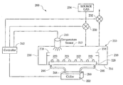
- FIG. 2 illustrates a cross section view of a loadlock chamber 200 , which may be used as one or more of the loadlock chambers 121 of FIG. 1 , in accordance with an embodiment of the present invention.
- a loadlock chamber 200 which may be used as one or more of the loadlock chambers 121 of FIG. 1 , in accordance with an embodiment of the present invention.
- FIG. 2 schematically illustrates an embodiment of the present invention and an actual embodiment of the invention may take any shape or form.
- the loadlock chamber 200 comprises an enclosed chamber 210 having a top 212 , a bottom 214 , and sidewalls 216 .
- Holders 218 are positioned to hold one or more wafers during transport.
- a temperature-controlled plate 220 is positioned along the bottom 214 and is coupled to an adjustable chiller 222 .
- the chiller 222 provides cooling water via a chiller output port 248 to the temperature-controlled plate 220 via a temperature-controlled plate input port 244 , and the cooling water is returned from the temperature-controlled plate 220 via a temperature-controlled plate output port 246 to the chiller 222 via a chiller input port 250 .
- the chiller 222 is adjustable to supply a cooling liquid, such as water, having an adjustable temperature to the temperature-controlled plate 220 .
- the chiller 222 may also be adjusted to provide the cooling liquid at an adjustable pressure.
- the temperature-controlled plate 220 includes tubing made of a material having good thermal conductivity properties. In an embodiment, copper tubing is used and the chiller 222 is adjustable to provide the cooling liquid having a temperature from about 17° C. to about 120° C., but more preferably from about 30° C. to about 90° C. Additionally, it is preferred that the chiller 222 and the temperature-controlled plate 220 are a pressurized system having a pressure ranging from about 1 atm to about 10 atm.
- the temperature-controlled plate 220 may also include raised portions, such as a plurality of pins 223 upon which a wafer may rest.
- the height of the plurality of pins 223 may be adjusted to maximize the cooling effect, including the rate of cooling, needed for a particular application. For example, it has been found that the height of the pins may be reduced to shorten the period of time required to cool the wafer to a specific temperature.
- the height of the plurality of pins 223 is between about 1 mm and about 0.1 mm. Other heights, however, may be used. It should also be noted that other shapes may be used.
- the pins may be any shape and may comprise ridges or a spiral shape on the temperature-controlled plate 220 .
- FIG. 2 also illustrates a mass flow controller 230 and a control valve 232 in accordance with an embodiment of the present invention.
- the mass flow controller 230 and the control valve 232 act together to create and maintain a gas atmosphere within the loadlock chamber 200 .
- the mass flow controller 230 is coupled to a source gas 234 to control the flow of gas into the loadlock chamber 200
- the control valve 232 is coupled to the loadlock chamber 200 to release gas from within the loadlock chamber 200 by pump.
- the mass flow controller 230 and the control valve 232 cooperate to maintain a specific pressure within the loadlock chamber 200 .
- the mass flow controller 230 and the control valve 232 are configured to maintain an atmospheric pressure within the loadlock chamber 200 from about 3 Torr to about 760 Torr.
- the loadlock chamber 200 includes a temperature sensor 240 , such as an infra-red temperature sensor, communicatively coupled to a controller 242 , which may also be communicatively coupled to the chiller 222 , the mass flow controller 230 , and/or the control valve 232 .
- the controller 242 receives temperature information from the temperature sensor 240 and automatically controls the chiller 222 , the mass flow controller 230 , and/or the control valve 232 to maintain a desired temperature.
- the desired temperature may be based upon, among other things, the previous process, the subsequent process, the wafer size and thickness, and the like.
- FIG. 2 illustrates a single temperature sensor 240 for illustrative purposes only. It may be desirable in some embodiments of the present invention to utilize multiple temperature sensors, and possibly different types of temperature sensors. For example, multiple temperature sensors may be positioned in various locations within the loadlock chamber 200 to provide temperature measurements in various regions of the wafer. The locations may include, for example, various locations across the wafer as well as both sides of the wafer.
- FIG. 3 is a flow diagram illustrating a procedure that may be performed to control the temperature of a wafer in accordance with an embodiment of the present invention.
- the process begins in step 305 , wherein a desired temperature is set.
- the desired temperature may be set by a user, read from a database, or the like. It should be noted that the desired temperature may be based upon the process or processes being performed on the wafer. For example, the desired temperature may be set to a first temperature immediately after a first process has been performed to cause the temperature of the wafer to decrease slowly or quickly, or to cause the temperature of the wafer to increase slowly or quickly. A second process may require different temperatures. As another example, it may be desirable to maintain a specific wafer temperature prior to performing a specific process.
- the process then proceeds to step 310 , wherein one or more temperature samples are received.
- the temperature samples may be received from a single temperature sensor or from multiple temperature sensors placed in different locations within the loadlock chamber 200 .
- temperature sensors may be placed across the top surface 212 of the loadlock chamber 200 spaced apart such that the temperature sensors measure different portions of the wafer, including around the perimeter and the interior of the wafer. Additional temperature sensors may be placed to measure the temperature along the bottom of the wafer.
- step 312 a determination is made whether or not the temperature needs adjusting.
- the desired temperature (see step 305 ) is compared to the temperature samples and an adjustment, if necessary, is determined. If a determination is made that an adjustment is necessary, then processing proceeds to step 314 , wherein an adjustment is made.
- the adjustment may include, for example, increasing the gas flow and pressure via the mass flow controller 230 , reducing the gas flow and pressure via the mass flow controller 230 and the control valve 232 , adjusting the temperature of the cooling fluid supplied by the chiller 222 , adjusting the flow rate of the cooling fluid supplied by the chiller 222 , and/or the like.
- step 312 If in step 312 a determination is made that an adjustment is not necessary, then processing returns to step 310 , wherein new temperature samples are received for processing.
- an embodiment of the present invention may utilize an adjustable chiller, another embodiment of the present invention may utilize an adjustable chiller with a temperature sensor, another embodiment of the present invention may utilize a mass flow controller to maintain a specific temperature, another embodiment of the present invention may utilize a mass flow controller with a temperature sensor, and another embodiment may utilize an adjustable chiller, a mass flow controller, and a temperature sensor.
- temperature controlled loadlock chamber provides dynamic controls and a feedback loop for maintaining optimum temperatures for a specific process. In this manner, more uniform semiconductor devices, including more uniform gate dielectrics, may be created. The increased uniformity will enable more accurate and uniform circuits to be created.
Landscapes
- Engineering & Computer Science (AREA)
- Physics & Mathematics (AREA)
- Condensed Matter Physics & Semiconductors (AREA)
- General Physics & Mathematics (AREA)
- Manufacturing & Machinery (AREA)
- Computer Hardware Design (AREA)
- Microelectronics & Electronic Packaging (AREA)
- Power Engineering (AREA)
- Container, Conveyance, Adherence, Positioning, Of Wafer (AREA)
- Chemical Vapour Deposition (AREA)
Abstract
Description
Claims (15)
Priority Applications (3)
| Application Number | Priority Date | Filing Date | Title |
|---|---|---|---|
| US11/769,589 US8905124B2 (en) | 2007-06-27 | 2007-06-27 | Temperature controlled loadlock chamber |
| CN2008100002374A CN101335183B (en) | 2007-06-27 | 2008-01-24 | Temperature controlled loadlock chamber |
| US14/537,569 US9698030B2 (en) | 2007-06-27 | 2014-11-10 | Temperature controlled loadlock chamber |
Applications Claiming Priority (1)
| Application Number | Priority Date | Filing Date | Title |
|---|---|---|---|
| US11/769,589 US8905124B2 (en) | 2007-06-27 | 2007-06-27 | Temperature controlled loadlock chamber |
Related Child Applications (1)
| Application Number | Title | Priority Date | Filing Date |
|---|---|---|---|
| US14/537,569 Continuation US9698030B2 (en) | 2007-06-27 | 2014-11-10 | Temperature controlled loadlock chamber |
Publications (2)
| Publication Number | Publication Date |
|---|---|
| US20090000769A1 US20090000769A1 (en) | 2009-01-01 |
| US8905124B2 true US8905124B2 (en) | 2014-12-09 |
Family
ID=40158992
Family Applications (2)
| Application Number | Title | Priority Date | Filing Date |
|---|---|---|---|
| US11/769,589 Active 2030-12-03 US8905124B2 (en) | 2007-06-27 | 2007-06-27 | Temperature controlled loadlock chamber |
| US14/537,569 Active US9698030B2 (en) | 2007-06-27 | 2014-11-10 | Temperature controlled loadlock chamber |
Family Applications After (1)
| Application Number | Title | Priority Date | Filing Date |
|---|---|---|---|
| US14/537,569 Active US9698030B2 (en) | 2007-06-27 | 2014-11-10 | Temperature controlled loadlock chamber |
Country Status (2)
| Country | Link |
|---|---|
| US (2) | US8905124B2 (en) |
| CN (1) | CN101335183B (en) |
Families Citing this family (257)
| Publication number | Priority date | Publication date | Assignee | Title |
|---|---|---|---|---|
| US9394608B2 (en) | 2009-04-06 | 2016-07-19 | Asm America, Inc. | Semiconductor processing reactor and components thereof |
| US8802201B2 (en) | 2009-08-14 | 2014-08-12 | Asm America, Inc. | Systems and methods for thin-film deposition of metal oxides using excited nitrogen-oxygen species |
| US9312155B2 (en) | 2011-06-06 | 2016-04-12 | Asm Japan K.K. | High-throughput semiconductor-processing apparatus equipped with multiple dual-chamber modules |
| US10854498B2 (en) | 2011-07-15 | 2020-12-01 | Asm Ip Holding B.V. | Wafer-supporting device and method for producing same |
| US20130023129A1 (en) | 2011-07-20 | 2013-01-24 | Asm America, Inc. | Pressure transmitter for a semiconductor processing environment |
| US9017481B1 (en) | 2011-10-28 | 2015-04-28 | Asm America, Inc. | Process feed management for semiconductor substrate processing |
| US10714315B2 (en) | 2012-10-12 | 2020-07-14 | Asm Ip Holdings B.V. | Semiconductor reaction chamber showerhead |
| US9773918B2 (en) * | 2012-12-18 | 2017-09-26 | Cbrite Inc. | Metal oxide TFT with improved stability and mobility |
| US20160376700A1 (en) | 2013-02-01 | 2016-12-29 | Asm Ip Holding B.V. | System for treatment of deposition reactor |
| US10683571B2 (en) | 2014-02-25 | 2020-06-16 | Asm Ip Holding B.V. | Gas supply manifold and method of supplying gases to chamber using same |
| US10167557B2 (en) | 2014-03-18 | 2019-01-01 | Asm Ip Holding B.V. | Gas distribution system, reactor including the system, and methods of using the same |
| US11015245B2 (en) | 2014-03-19 | 2021-05-25 | Asm Ip Holding B.V. | Gas-phase reactor and system having exhaust plenum and components thereof |
| US10858737B2 (en) | 2014-07-28 | 2020-12-08 | Asm Ip Holding B.V. | Showerhead assembly and components thereof |
| US9890456B2 (en) | 2014-08-21 | 2018-02-13 | Asm Ip Holding B.V. | Method and system for in situ formation of gas-phase compounds |
| US10941490B2 (en) | 2014-10-07 | 2021-03-09 | Asm Ip Holding B.V. | Multiple temperature range susceptor, assembly, reactor and system including the susceptor, and methods of using the same |
| TW201639063A (en) | 2015-01-22 | 2016-11-01 | 應用材料股份有限公司 | Batch heating and cooling chamber or loadlock |
| US10276355B2 (en) | 2015-03-12 | 2019-04-30 | Asm Ip Holding B.V. | Multi-zone reactor, system including the reactor, and method of using the same |
| US10458018B2 (en) | 2015-06-26 | 2019-10-29 | Asm Ip Holding B.V. | Structures including metal carbide material, devices including the structures, and methods of forming same |
| US10600673B2 (en) | 2015-07-07 | 2020-03-24 | Asm Ip Holding B.V. | Magnetic susceptor to baseplate seal |
| US10211308B2 (en) | 2015-10-21 | 2019-02-19 | Asm Ip Holding B.V. | NbMC layers |
| US11139308B2 (en) | 2015-12-29 | 2021-10-05 | Asm Ip Holding B.V. | Atomic layer deposition of III-V compounds to form V-NAND devices |
| US10529554B2 (en) | 2016-02-19 | 2020-01-07 | Asm Ip Holding B.V. | Method for forming silicon nitride film selectively on sidewalls or flat surfaces of trenches |
| US10865475B2 (en) | 2016-04-21 | 2020-12-15 | Asm Ip Holding B.V. | Deposition of metal borides and silicides |
| US10190213B2 (en) | 2016-04-21 | 2019-01-29 | Asm Ip Holding B.V. | Deposition of metal borides |
| US10032628B2 (en) | 2016-05-02 | 2018-07-24 | Asm Ip Holding B.V. | Source/drain performance through conformal solid state doping |
| US10367080B2 (en) | 2016-05-02 | 2019-07-30 | Asm Ip Holding B.V. | Method of forming a germanium oxynitride film |
| US11453943B2 (en) | 2016-05-25 | 2022-09-27 | Asm Ip Holding B.V. | Method for forming carbon-containing silicon/metal oxide or nitride film by ALD using silicon precursor and hydrocarbon precursor |
| US10612137B2 (en) | 2016-07-08 | 2020-04-07 | Asm Ip Holdings B.V. | Organic reactants for atomic layer deposition |
| US9859151B1 (en) | 2016-07-08 | 2018-01-02 | Asm Ip Holding B.V. | Selective film deposition method to form air gaps |
| US10714385B2 (en) | 2016-07-19 | 2020-07-14 | Asm Ip Holding B.V. | Selective deposition of tungsten |
| US9887082B1 (en) | 2016-07-28 | 2018-02-06 | Asm Ip Holding B.V. | Method and apparatus for filling a gap |
| KR102532607B1 (en) | 2016-07-28 | 2023-05-15 | 에이에스엠 아이피 홀딩 비.브이. | Substrate processing apparatus and method of operating the same |
| US9812320B1 (en) | 2016-07-28 | 2017-11-07 | Asm Ip Holding B.V. | Method and apparatus for filling a gap |
| CN106339014B (en) * | 2016-10-13 | 2019-01-08 | 深圳市建恒测控股份有限公司 | A kind of control method of constant temperature system |
| US10643826B2 (en) | 2016-10-26 | 2020-05-05 | Asm Ip Holdings B.V. | Methods for thermally calibrating reaction chambers |
| US11532757B2 (en) | 2016-10-27 | 2022-12-20 | Asm Ip Holding B.V. | Deposition of charge trapping layers |
| US10229833B2 (en) | 2016-11-01 | 2019-03-12 | Asm Ip Holding B.V. | Methods for forming a transition metal nitride film on a substrate by atomic layer deposition and related semiconductor device structures |
| US10643904B2 (en) | 2016-11-01 | 2020-05-05 | Asm Ip Holdings B.V. | Methods for forming a semiconductor device and related semiconductor device structures |
| US10714350B2 (en) | 2016-11-01 | 2020-07-14 | ASM IP Holdings, B.V. | Methods for forming a transition metal niobium nitride film on a substrate by atomic layer deposition and related semiconductor device structures |
| KR102546317B1 (en) | 2016-11-15 | 2023-06-21 | 에이에스엠 아이피 홀딩 비.브이. | Gas supply unit and substrate processing apparatus including the same |
| KR20180068582A (en) | 2016-12-14 | 2018-06-22 | 에이에스엠 아이피 홀딩 비.브이. | Substrate processing apparatus |
| US11581186B2 (en) | 2016-12-15 | 2023-02-14 | Asm Ip Holding B.V. | Sequential infiltration synthesis apparatus |
| US11447861B2 (en) | 2016-12-15 | 2022-09-20 | Asm Ip Holding B.V. | Sequential infiltration synthesis apparatus and a method of forming a patterned structure |
| KR20180070971A (en) | 2016-12-19 | 2018-06-27 | 에이에스엠 아이피 홀딩 비.브이. | Substrate processing apparatus |
| US10269558B2 (en) | 2016-12-22 | 2019-04-23 | Asm Ip Holding B.V. | Method of forming a structure on a substrate |
| US10867788B2 (en) | 2016-12-28 | 2020-12-15 | Asm Ip Holding B.V. | Method of forming a structure on a substrate |
| US11390950B2 (en) | 2017-01-10 | 2022-07-19 | Asm Ip Holding B.V. | Reactor system and method to reduce residue buildup during a film deposition process |
| US10655221B2 (en) | 2017-02-09 | 2020-05-19 | Asm Ip Holding B.V. | Method for depositing oxide film by thermal ALD and PEALD |
| US10468261B2 (en) | 2017-02-15 | 2019-11-05 | Asm Ip Holding B.V. | Methods for forming a metallic film on a substrate by cyclical deposition and related semiconductor device structures |
| US10529563B2 (en) | 2017-03-29 | 2020-01-07 | Asm Ip Holdings B.V. | Method for forming doped metal oxide films on a substrate by cyclical deposition and related semiconductor device structures |
| KR102457289B1 (en) | 2017-04-25 | 2022-10-21 | 에이에스엠 아이피 홀딩 비.브이. | Method for depositing a thin film and manufacturing a semiconductor device |
| US10892156B2 (en) | 2017-05-08 | 2021-01-12 | Asm Ip Holding B.V. | Methods for forming a silicon nitride film on a substrate and related semiconductor device structures |
| US10770286B2 (en) | 2017-05-08 | 2020-09-08 | Asm Ip Holdings B.V. | Methods for selectively forming a silicon nitride film on a substrate and related semiconductor device structures |
| US11306395B2 (en) | 2017-06-28 | 2022-04-19 | Asm Ip Holding B.V. | Methods for depositing a transition metal nitride film on a substrate by atomic layer deposition and related deposition apparatus |
| US10685834B2 (en) | 2017-07-05 | 2020-06-16 | Asm Ip Holdings B.V. | Methods for forming a silicon germanium tin layer and related semiconductor device structures |
| KR20190009245A (en) | 2017-07-18 | 2019-01-28 | 에이에스엠 아이피 홀딩 비.브이. | Methods for forming a semiconductor device structure and related semiconductor device structures |
| US11374112B2 (en) | 2017-07-19 | 2022-06-28 | Asm Ip Holding B.V. | Method for depositing a group IV semiconductor and related semiconductor device structures |
| US11018002B2 (en) | 2017-07-19 | 2021-05-25 | Asm Ip Holding B.V. | Method for selectively depositing a Group IV semiconductor and related semiconductor device structures |
| US10541333B2 (en) | 2017-07-19 | 2020-01-21 | Asm Ip Holding B.V. | Method for depositing a group IV semiconductor and related semiconductor device structures |
| US10590535B2 (en) | 2017-07-26 | 2020-03-17 | Asm Ip Holdings B.V. | Chemical treatment, deposition and/or infiltration apparatus and method for using the same |
| US10692741B2 (en) | 2017-08-08 | 2020-06-23 | Asm Ip Holdings B.V. | Radiation shield |
| US10770336B2 (en) | 2017-08-08 | 2020-09-08 | Asm Ip Holding B.V. | Substrate lift mechanism and reactor including same |
| US11769682B2 (en) | 2017-08-09 | 2023-09-26 | Asm Ip Holding B.V. | Storage apparatus for storing cassettes for substrates and processing apparatus equipped therewith |
| US10249524B2 (en) | 2017-08-09 | 2019-04-02 | Asm Ip Holding B.V. | Cassette holder assembly for a substrate cassette and holding member for use in such assembly |
| US11139191B2 (en) | 2017-08-09 | 2021-10-05 | Asm Ip Holding B.V. | Storage apparatus for storing cassettes for substrates and processing apparatus equipped therewith |
| USD900036S1 (en) | 2017-08-24 | 2020-10-27 | Asm Ip Holding B.V. | Heater electrical connector and adapter |
| US11830730B2 (en) | 2017-08-29 | 2023-11-28 | Asm Ip Holding B.V. | Layer forming method and apparatus |
| KR102491945B1 (en) | 2017-08-30 | 2023-01-26 | 에이에스엠 아이피 홀딩 비.브이. | Substrate processing apparatus |
| US11295980B2 (en) | 2017-08-30 | 2022-04-05 | Asm Ip Holding B.V. | Methods for depositing a molybdenum metal film over a dielectric surface of a substrate by a cyclical deposition process and related semiconductor device structures |
| US11056344B2 (en) | 2017-08-30 | 2021-07-06 | Asm Ip Holding B.V. | Layer forming method |
| KR102630301B1 (en) | 2017-09-21 | 2024-01-29 | 에이에스엠 아이피 홀딩 비.브이. | Method of sequential infiltration synthesis treatment of infiltrateable material and structures and devices formed using same |
| US10844484B2 (en) | 2017-09-22 | 2020-11-24 | Asm Ip Holding B.V. | Apparatus for dispensing a vapor phase reactant to a reaction chamber and related methods |
| US10658205B2 (en) | 2017-09-28 | 2020-05-19 | Asm Ip Holdings B.V. | Chemical dispensing apparatus and methods for dispensing a chemical to a reaction chamber |
| US10403504B2 (en) | 2017-10-05 | 2019-09-03 | Asm Ip Holding B.V. | Method for selectively depositing a metallic film on a substrate |
| US10319588B2 (en) | 2017-10-10 | 2019-06-11 | Asm Ip Holding B.V. | Method for depositing a metal chalcogenide on a substrate by cyclical deposition |
| US10923344B2 (en) | 2017-10-30 | 2021-02-16 | Asm Ip Holding B.V. | Methods for forming a semiconductor structure and related semiconductor structures |
| US10910262B2 (en) | 2017-11-16 | 2021-02-02 | Asm Ip Holding B.V. | Method of selectively depositing a capping layer structure on a semiconductor device structure |
| KR102443047B1 (en) | 2017-11-16 | 2022-09-14 | 에이에스엠 아이피 홀딩 비.브이. | Method of processing a substrate and a device manufactured by the same |
| US11022879B2 (en) | 2017-11-24 | 2021-06-01 | Asm Ip Holding B.V. | Method of forming an enhanced unexposed photoresist layer |
| US11639811B2 (en) | 2017-11-27 | 2023-05-02 | Asm Ip Holding B.V. | Apparatus including a clean mini environment |
| KR102597978B1 (en) | 2017-11-27 | 2023-11-06 | 에이에스엠 아이피 홀딩 비.브이. | Storage device for storing wafer cassettes for use with batch furnaces |
| US10872771B2 (en) | 2018-01-16 | 2020-12-22 | Asm Ip Holding B. V. | Method for depositing a material film on a substrate within a reaction chamber by a cyclical deposition process and related device structures |
| US11482412B2 (en) | 2018-01-19 | 2022-10-25 | Asm Ip Holding B.V. | Method for depositing a gap-fill layer by plasma-assisted deposition |
| TW202325889A (en) | 2018-01-19 | 2023-07-01 | 荷蘭商Asm 智慧財產控股公司 | Deposition method |
| USD903477S1 (en) | 2018-01-24 | 2020-12-01 | Asm Ip Holdings B.V. | Metal clamp |
| US11018047B2 (en) | 2018-01-25 | 2021-05-25 | Asm Ip Holding B.V. | Hybrid lift pin |
| USD880437S1 (en) | 2018-02-01 | 2020-04-07 | Asm Ip Holding B.V. | Gas supply plate for semiconductor manufacturing apparatus |
| US11081345B2 (en) | 2018-02-06 | 2021-08-03 | Asm Ip Holding B.V. | Method of post-deposition treatment for silicon oxide film |
| WO2019158960A1 (en) | 2018-02-14 | 2019-08-22 | Asm Ip Holding B.V. | A method for depositing a ruthenium-containing film on a substrate by a cyclical deposition process |
| US10896820B2 (en) | 2018-02-14 | 2021-01-19 | Asm Ip Holding B.V. | Method for depositing a ruthenium-containing film on a substrate by a cyclical deposition process |
| US10731249B2 (en) | 2018-02-15 | 2020-08-04 | Asm Ip Holding B.V. | Method of forming a transition metal containing film on a substrate by a cyclical deposition process, a method for supplying a transition metal halide compound to a reaction chamber, and related vapor deposition apparatus |
| US10658181B2 (en) | 2018-02-20 | 2020-05-19 | Asm Ip Holding B.V. | Method of spacer-defined direct patterning in semiconductor fabrication |
| KR102636427B1 (en) | 2018-02-20 | 2024-02-13 | 에이에스엠 아이피 홀딩 비.브이. | Substrate processing method and apparatus |
| US10975470B2 (en) | 2018-02-23 | 2021-04-13 | Asm Ip Holding B.V. | Apparatus for detecting or monitoring for a chemical precursor in a high temperature environment |
| US11473195B2 (en) | 2018-03-01 | 2022-10-18 | Asm Ip Holding B.V. | Semiconductor processing apparatus and a method for processing a substrate |
| US11629406B2 (en) * | 2018-03-09 | 2023-04-18 | Asm Ip Holding B.V. | Semiconductor processing apparatus comprising one or more pyrometers for measuring a temperature of a substrate during transfer of the substrate |
| US11114283B2 (en) | 2018-03-16 | 2021-09-07 | Asm Ip Holding B.V. | Reactor, system including the reactor, and methods of manufacturing and using same |
| KR102646467B1 (en) | 2018-03-27 | 2024-03-11 | 에이에스엠 아이피 홀딩 비.브이. | Method of forming an electrode on a substrate and a semiconductor device structure including an electrode |
| US11088002B2 (en) | 2018-03-29 | 2021-08-10 | Asm Ip Holding B.V. | Substrate rack and a substrate processing system and method |
| US11230766B2 (en) | 2018-03-29 | 2022-01-25 | Asm Ip Holding B.V. | Substrate processing apparatus and method |
| KR102501472B1 (en) | 2018-03-30 | 2023-02-20 | 에이에스엠 아이피 홀딩 비.브이. | Substrate processing method |
| TWI811348B (en) | 2018-05-08 | 2023-08-11 | 荷蘭商Asm 智慧財產控股公司 | Methods for depositing an oxide film on a substrate by a cyclical deposition process and related device structures |
| TWI816783B (en) | 2018-05-11 | 2023-10-01 | 荷蘭商Asm 智慧財產控股公司 | Methods for forming a doped metal carbide film on a substrate and related semiconductor device structures |
| KR102596988B1 (en) | 2018-05-28 | 2023-10-31 | 에이에스엠 아이피 홀딩 비.브이. | Method of processing a substrate and a device manufactured by the same |
| US11718913B2 (en) | 2018-06-04 | 2023-08-08 | Asm Ip Holding B.V. | Gas distribution system and reactor system including same |
| US11270899B2 (en) | 2018-06-04 | 2022-03-08 | Asm Ip Holding B.V. | Wafer handling chamber with moisture reduction |
| US11286562B2 (en) | 2018-06-08 | 2022-03-29 | Asm Ip Holding B.V. | Gas-phase chemical reactor and method of using same |
| KR102568797B1 (en) | 2018-06-21 | 2023-08-21 | 에이에스엠 아이피 홀딩 비.브이. | Substrate processing system |
| US10797133B2 (en) | 2018-06-21 | 2020-10-06 | Asm Ip Holding B.V. | Method for depositing a phosphorus doped silicon arsenide film and related semiconductor device structures |
| CN112292477A (en) | 2018-06-27 | 2021-01-29 | Asm Ip私人控股有限公司 | Cyclic deposition methods for forming metal-containing materials and films and structures containing metal-containing materials |
| JP2021529254A (en) | 2018-06-27 | 2021-10-28 | エーエスエム・アイピー・ホールディング・ベー・フェー | Periodic deposition methods for forming metal-containing materials and films and structures containing metal-containing materials |
| KR20200002519A (en) | 2018-06-29 | 2020-01-08 | 에이에스엠 아이피 홀딩 비.브이. | Method for depositing a thin film and manufacturing a semiconductor device |
| US10612136B2 (en) | 2018-06-29 | 2020-04-07 | ASM IP Holding, B.V. | Temperature-controlled flange and reactor system including same |
| US10755922B2 (en) | 2018-07-03 | 2020-08-25 | Asm Ip Holding B.V. | Method for depositing silicon-free carbon-containing film as gap-fill layer by pulse plasma-assisted deposition |
| US10388513B1 (en) | 2018-07-03 | 2019-08-20 | Asm Ip Holding B.V. | Method for depositing silicon-free carbon-containing film as gap-fill layer by pulse plasma-assisted deposition |
| US10767789B2 (en) | 2018-07-16 | 2020-09-08 | Asm Ip Holding B.V. | Diaphragm valves, valve components, and methods for forming valve components |
| US11053591B2 (en) | 2018-08-06 | 2021-07-06 | Asm Ip Holding B.V. | Multi-port gas injection system and reactor system including same |
| US10883175B2 (en) | 2018-08-09 | 2021-01-05 | Asm Ip Holding B.V. | Vertical furnace for processing substrates and a liner for use therein |
| US10829852B2 (en) | 2018-08-16 | 2020-11-10 | Asm Ip Holding B.V. | Gas distribution device for a wafer processing apparatus |
| US11430674B2 (en) | 2018-08-22 | 2022-08-30 | Asm Ip Holding B.V. | Sensor array, apparatus for dispensing a vapor phase reactant to a reaction chamber and related methods |
| KR20200030162A (en) | 2018-09-11 | 2020-03-20 | 에이에스엠 아이피 홀딩 비.브이. | Method for deposition of a thin film |
| US11024523B2 (en) | 2018-09-11 | 2021-06-01 | Asm Ip Holding B.V. | Substrate processing apparatus and method |
| US11049751B2 (en) | 2018-09-14 | 2021-06-29 | Asm Ip Holding B.V. | Cassette supply system to store and handle cassettes and processing apparatus equipped therewith |
| CN110970344A (en) | 2018-10-01 | 2020-04-07 | Asm Ip控股有限公司 | Substrate holding apparatus, system including the same, and method of using the same |
| US11232963B2 (en) | 2018-10-03 | 2022-01-25 | Asm Ip Holding B.V. | Substrate processing apparatus and method |
| KR102592699B1 (en) | 2018-10-08 | 2023-10-23 | 에이에스엠 아이피 홀딩 비.브이. | Substrate support unit and apparatuses for depositing thin film and processing the substrate including the same |
| US10847365B2 (en) | 2018-10-11 | 2020-11-24 | Asm Ip Holding B.V. | Method of forming conformal silicon carbide film by cyclic CVD |
| US10811256B2 (en) | 2018-10-16 | 2020-10-20 | Asm Ip Holding B.V. | Method for etching a carbon-containing feature |
| KR102605121B1 (en) | 2018-10-19 | 2023-11-23 | 에이에스엠 아이피 홀딩 비.브이. | Substrate processing apparatus and substrate processing method |
| KR102546322B1 (en) | 2018-10-19 | 2023-06-21 | 에이에스엠 아이피 홀딩 비.브이. | Substrate processing apparatus and substrate processing method |
| USD948463S1 (en) | 2018-10-24 | 2022-04-12 | Asm Ip Holding B.V. | Susceptor for semiconductor substrate supporting apparatus |
| US11087997B2 (en) | 2018-10-31 | 2021-08-10 | Asm Ip Holding B.V. | Substrate processing apparatus for processing substrates |
| KR20200051105A (en) | 2018-11-02 | 2020-05-13 | 에이에스엠 아이피 홀딩 비.브이. | Substrate support unit and substrate processing apparatus including the same |
| US11572620B2 (en) | 2018-11-06 | 2023-02-07 | Asm Ip Holding B.V. | Methods for selectively depositing an amorphous silicon film on a substrate |
| US11031242B2 (en) | 2018-11-07 | 2021-06-08 | Asm Ip Holding B.V. | Methods for depositing a boron doped silicon germanium film |
| US10847366B2 (en) | 2018-11-16 | 2020-11-24 | Asm Ip Holding B.V. | Methods for depositing a transition metal chalcogenide film on a substrate by a cyclical deposition process |
| US10818758B2 (en) | 2018-11-16 | 2020-10-27 | Asm Ip Holding B.V. | Methods for forming a metal silicate film on a substrate in a reaction chamber and related semiconductor device structures |
| US11217444B2 (en) | 2018-11-30 | 2022-01-04 | Asm Ip Holding B.V. | Method for forming an ultraviolet radiation responsive metal oxide-containing film |
| KR102636428B1 (en) | 2018-12-04 | 2024-02-13 | 에이에스엠 아이피 홀딩 비.브이. | A method for cleaning a substrate processing apparatus |
| US11158513B2 (en) | 2018-12-13 | 2021-10-26 | Asm Ip Holding B.V. | Methods for forming a rhenium-containing film on a substrate by a cyclical deposition process and related semiconductor device structures |
| JP2020096183A (en) | 2018-12-14 | 2020-06-18 | エーエスエム・アイピー・ホールディング・ベー・フェー | Method of forming device structure using selective deposition of gallium nitride, and system for the same |
| TWI819180B (en) | 2019-01-17 | 2023-10-21 | 荷蘭商Asm 智慧財產控股公司 | Methods of forming a transition metal containing film on a substrate by a cyclical deposition process |
| KR20200091543A (en) | 2019-01-22 | 2020-07-31 | 에이에스엠 아이피 홀딩 비.브이. | Semiconductor processing device |
| CN111524788B (en) | 2019-02-01 | 2023-11-24 | Asm Ip私人控股有限公司 | Method for topologically selective film formation of silicon oxide |
| KR102626263B1 (en) | 2019-02-20 | 2024-01-16 | 에이에스엠 아이피 홀딩 비.브이. | Cyclical deposition method including treatment step and apparatus for same |
| JP2020136677A (en) | 2019-02-20 | 2020-08-31 | エーエスエム・アイピー・ホールディング・ベー・フェー | Periodic accumulation method for filing concave part formed inside front surface of base material, and device |
| KR102638425B1 (en) | 2019-02-20 | 2024-02-21 | 에이에스엠 아이피 홀딩 비.브이. | Method and apparatus for filling a recess formed within a substrate surface |
| US11482533B2 (en) | 2019-02-20 | 2022-10-25 | Asm Ip Holding B.V. | Apparatus and methods for plug fill deposition in 3-D NAND applications |
| JP2020133004A (en) | 2019-02-22 | 2020-08-31 | エーエスエム・アイピー・ホールディング・ベー・フェー | Base material processing apparatus and method for processing base material |
| KR20200108243A (en) | 2019-03-08 | 2020-09-17 | 에이에스엠 아이피 홀딩 비.브이. | Structure Including SiOC Layer and Method of Forming Same |
| KR20200108242A (en) | 2019-03-08 | 2020-09-17 | 에이에스엠 아이피 홀딩 비.브이. | Method for Selective Deposition of Silicon Nitride Layer and Structure Including Selectively-Deposited Silicon Nitride Layer |
| US11742198B2 (en) | 2019-03-08 | 2023-08-29 | Asm Ip Holding B.V. | Structure including SiOCN layer and method of forming same |
| JP2020167398A (en) | 2019-03-28 | 2020-10-08 | エーエスエム・アイピー・ホールディング・ベー・フェー | Door opener and substrate processing apparatus provided therewith |
| KR20200116855A (en) | 2019-04-01 | 2020-10-13 | 에이에스엠 아이피 홀딩 비.브이. | Method of manufacturing semiconductor device |
| US11447864B2 (en) | 2019-04-19 | 2022-09-20 | Asm Ip Holding B.V. | Layer forming method and apparatus |
| KR20200125453A (en) | 2019-04-24 | 2020-11-04 | 에이에스엠 아이피 홀딩 비.브이. | Gas-phase reactor system and method of using same |
| KR20200130121A (en) | 2019-05-07 | 2020-11-18 | 에이에스엠 아이피 홀딩 비.브이. | Chemical source vessel with dip tube |
| KR20200130118A (en) | 2019-05-07 | 2020-11-18 | 에이에스엠 아이피 홀딩 비.브이. | Method for Reforming Amorphous Carbon Polymer Film |
| KR20200130652A (en) | 2019-05-10 | 2020-11-19 | 에이에스엠 아이피 홀딩 비.브이. | Method of depositing material onto a surface and structure formed according to the method |
| JP2020188255A (en) | 2019-05-16 | 2020-11-19 | エーエスエム アイピー ホールディング ビー.ブイ. | Wafer boat handling device, vertical batch furnace, and method |
| USD975665S1 (en) | 2019-05-17 | 2023-01-17 | Asm Ip Holding B.V. | Susceptor shaft |
| USD947913S1 (en) | 2019-05-17 | 2022-04-05 | Asm Ip Holding B.V. | Susceptor shaft |
| USD935572S1 (en) | 2019-05-24 | 2021-11-09 | Asm Ip Holding B.V. | Gas channel plate |
| USD922229S1 (en) | 2019-06-05 | 2021-06-15 | Asm Ip Holding B.V. | Device for controlling a temperature of a gas supply unit |
| KR20200141002A (en) | 2019-06-06 | 2020-12-17 | 에이에스엠 아이피 홀딩 비.브이. | Method of using a gas-phase reactor system including analyzing exhausted gas |
| KR20200143254A (en) | 2019-06-11 | 2020-12-23 | 에이에스엠 아이피 홀딩 비.브이. | Method of forming an electronic structure using an reforming gas, system for performing the method, and structure formed using the method |
| USD944946S1 (en) | 2019-06-14 | 2022-03-01 | Asm Ip Holding B.V. | Shower plate |
| USD931978S1 (en) | 2019-06-27 | 2021-09-28 | Asm Ip Holding B.V. | Showerhead vacuum transport |
| KR20210005515A (en) | 2019-07-03 | 2021-01-14 | 에이에스엠 아이피 홀딩 비.브이. | Temperature control assembly for substrate processing apparatus and method of using same |
| JP2021015791A (en) | 2019-07-09 | 2021-02-12 | エーエスエム アイピー ホールディング ビー.ブイ. | Plasma device and substrate processing method using coaxial waveguide |
| CN112216646A (en) | 2019-07-10 | 2021-01-12 | Asm Ip私人控股有限公司 | Substrate supporting assembly and substrate processing device comprising same |
| KR20210010307A (en) | 2019-07-16 | 2021-01-27 | 에이에스엠 아이피 홀딩 비.브이. | Substrate processing apparatus |
| KR20210010820A (en) | 2019-07-17 | 2021-01-28 | 에이에스엠 아이피 홀딩 비.브이. | Methods of forming silicon germanium structures |
| KR20210010816A (en) | 2019-07-17 | 2021-01-28 | 에이에스엠 아이피 홀딩 비.브이. | Radical assist ignition plasma system and method |
| US11643724B2 (en) | 2019-07-18 | 2023-05-09 | Asm Ip Holding B.V. | Method of forming structures using a neutral beam |
| CN112242296A (en) | 2019-07-19 | 2021-01-19 | Asm Ip私人控股有限公司 | Method of forming topologically controlled amorphous carbon polymer films |
| TW202113936A (en) | 2019-07-29 | 2021-04-01 | 荷蘭商Asm Ip私人控股有限公司 | Methods for selective deposition utilizing n-type dopants and/or alternative dopants to achieve high dopant incorporation |
| CN112309900A (en) | 2019-07-30 | 2021-02-02 | Asm Ip私人控股有限公司 | Substrate processing apparatus |
| CN112309899A (en) | 2019-07-30 | 2021-02-02 | Asm Ip私人控股有限公司 | Substrate processing apparatus |
| US11587814B2 (en) | 2019-07-31 | 2023-02-21 | Asm Ip Holding B.V. | Vertical batch furnace assembly |
| US11227782B2 (en) | 2019-07-31 | 2022-01-18 | Asm Ip Holding B.V. | Vertical batch furnace assembly |
| US11587815B2 (en) | 2019-07-31 | 2023-02-21 | Asm Ip Holding B.V. | Vertical batch furnace assembly |
| CN112323048B (en) | 2019-08-05 | 2024-02-09 | Asm Ip私人控股有限公司 | Liquid level sensor for chemical source container |
| USD965524S1 (en) | 2019-08-19 | 2022-10-04 | Asm Ip Holding B.V. | Susceptor support |
| USD965044S1 (en) | 2019-08-19 | 2022-09-27 | Asm Ip Holding B.V. | Susceptor shaft |
| JP2021031769A (en) | 2019-08-21 | 2021-03-01 | エーエスエム アイピー ホールディング ビー.ブイ. | Production apparatus of mixed gas of film deposition raw material and film deposition apparatus |
| USD940837S1 (en) | 2019-08-22 | 2022-01-11 | Asm Ip Holding B.V. | Electrode |
| USD979506S1 (en) | 2019-08-22 | 2023-02-28 | Asm Ip Holding B.V. | Insulator |
| KR20210024423A (en) | 2019-08-22 | 2021-03-05 | 에이에스엠 아이피 홀딩 비.브이. | Method for forming a structure with a hole |
| USD949319S1 (en) | 2019-08-22 | 2022-04-19 | Asm Ip Holding B.V. | Exhaust duct |
| USD930782S1 (en) | 2019-08-22 | 2021-09-14 | Asm Ip Holding B.V. | Gas distributor |
| US11286558B2 (en) | 2019-08-23 | 2022-03-29 | Asm Ip Holding B.V. | Methods for depositing a molybdenum nitride film on a surface of a substrate by a cyclical deposition process and related semiconductor device structures including a molybdenum nitride film |
| KR20210024420A (en) | 2019-08-23 | 2021-03-05 | 에이에스엠 아이피 홀딩 비.브이. | Method for depositing silicon oxide film having improved quality by peald using bis(diethylamino)silane |
| KR20210029090A (en) | 2019-09-04 | 2021-03-15 | 에이에스엠 아이피 홀딩 비.브이. | Methods for selective deposition using a sacrificial capping layer |
| KR20210029663A (en) | 2019-09-05 | 2021-03-16 | 에이에스엠 아이피 홀딩 비.브이. | Substrate processing apparatus |
| US11562901B2 (en) | 2019-09-25 | 2023-01-24 | Asm Ip Holding B.V. | Substrate processing method |
| CN112593212B (en) | 2019-10-02 | 2023-12-22 | Asm Ip私人控股有限公司 | Method for forming topologically selective silicon oxide film by cyclic plasma enhanced deposition process |
| TW202129060A (en) | 2019-10-08 | 2021-08-01 | 荷蘭商Asm Ip控股公司 | Substrate processing device, and substrate processing method |
| TW202115273A (en) | 2019-10-10 | 2021-04-16 | 荷蘭商Asm Ip私人控股有限公司 | Method of forming a photoresist underlayer and structure including same |
| KR20210045930A (en) | 2019-10-16 | 2021-04-27 | 에이에스엠 아이피 홀딩 비.브이. | Method of Topology-Selective Film Formation of Silicon Oxide |
| US11637014B2 (en) | 2019-10-17 | 2023-04-25 | Asm Ip Holding B.V. | Methods for selective deposition of doped semiconductor material |
| KR20210047808A (en) | 2019-10-21 | 2021-04-30 | 에이에스엠 아이피 홀딩 비.브이. | Apparatus and methods for selectively etching films |
| US11646205B2 (en) | 2019-10-29 | 2023-05-09 | Asm Ip Holding B.V. | Methods of selectively forming n-type doped material on a surface, systems for selectively forming n-type doped material, and structures formed using same |
| KR20210054983A (en) | 2019-11-05 | 2021-05-14 | 에이에스엠 아이피 홀딩 비.브이. | Structures with doped semiconductor layers and methods and systems for forming same |
| US11501968B2 (en) | 2019-11-15 | 2022-11-15 | Asm Ip Holding B.V. | Method for providing a semiconductor device with silicon filled gaps |
| KR20210062561A (en) | 2019-11-20 | 2021-05-31 | 에이에스엠 아이피 홀딩 비.브이. | Method of depositing carbon-containing material on a surface of a substrate, structure formed using the method, and system for forming the structure |
| US11450529B2 (en) | 2019-11-26 | 2022-09-20 | Asm Ip Holding B.V. | Methods for selectively forming a target film on a substrate comprising a first dielectric surface and a second metallic surface |
| CN112951697A (en) | 2019-11-26 | 2021-06-11 | Asm Ip私人控股有限公司 | Substrate processing apparatus |
| CN112885693A (en) | 2019-11-29 | 2021-06-01 | Asm Ip私人控股有限公司 | Substrate processing apparatus |
| CN112885692A (en) | 2019-11-29 | 2021-06-01 | Asm Ip私人控股有限公司 | Substrate processing apparatus |
| JP2021090042A (en) | 2019-12-02 | 2021-06-10 | エーエスエム アイピー ホールディング ビー.ブイ. | Substrate processing apparatus and substrate processing method |
| KR20210070898A (en) | 2019-12-04 | 2021-06-15 | 에이에스엠 아이피 홀딩 비.브이. | Substrate processing apparatus |
| JP2021097227A (en) | 2019-12-17 | 2021-06-24 | エーエスエム・アイピー・ホールディング・ベー・フェー | Method of forming vanadium nitride layer and structure including vanadium nitride layer |
| US11527403B2 (en) | 2019-12-19 | 2022-12-13 | Asm Ip Holding B.V. | Methods for filling a gap feature on a substrate surface and related semiconductor structures |
| JP2021109175A (en) | 2020-01-06 | 2021-08-02 | エーエスエム・アイピー・ホールディング・ベー・フェー | Gas supply assembly, components thereof, and reactor system including the same |
| KR20210095050A (en) | 2020-01-20 | 2021-07-30 | 에이에스엠 아이피 홀딩 비.브이. | Method of forming thin film and method of modifying surface of thin film |
| TW202130846A (en) | 2020-02-03 | 2021-08-16 | 荷蘭商Asm Ip私人控股有限公司 | Method of forming structures including a vanadium or indium layer |
| TW202146882A (en) | 2020-02-04 | 2021-12-16 | 荷蘭商Asm Ip私人控股有限公司 | Method of verifying an article, apparatus for verifying an article, and system for verifying a reaction chamber |
| US11776846B2 (en) | 2020-02-07 | 2023-10-03 | Asm Ip Holding B.V. | Methods for depositing gap filling fluids and related systems and devices |
| US11781243B2 (en) | 2020-02-17 | 2023-10-10 | Asm Ip Holding B.V. | Method for depositing low temperature phosphorous-doped silicon |
| TW202203344A (en) | 2020-02-28 | 2022-01-16 | 荷蘭商Asm Ip控股公司 | System dedicated for parts cleaning |
| US11876356B2 (en) | 2020-03-11 | 2024-01-16 | Asm Ip Holding B.V. | Lockout tagout assembly and system and method of using same |
| KR20210116240A (en) | 2020-03-11 | 2021-09-27 | 에이에스엠 아이피 홀딩 비.브이. | Substrate handling device with adjustable joints |
| CN113394086A (en) | 2020-03-12 | 2021-09-14 | Asm Ip私人控股有限公司 | Method for producing a layer structure having a target topological profile |
| KR20210124042A (en) | 2020-04-02 | 2021-10-14 | 에이에스엠 아이피 홀딩 비.브이. | Thin film forming method |
| TW202146689A (en) | 2020-04-03 | 2021-12-16 | 荷蘭商Asm Ip控股公司 | Method for forming barrier layer and method for manufacturing semiconductor device |
| TW202145344A (en) | 2020-04-08 | 2021-12-01 | 荷蘭商Asm Ip私人控股有限公司 | Apparatus and methods for selectively etching silcon oxide films |
| US11821078B2 (en) | 2020-04-15 | 2023-11-21 | Asm Ip Holding B.V. | Method for forming precoat film and method for forming silicon-containing film |
| TW202146831A (en) | 2020-04-24 | 2021-12-16 | 荷蘭商Asm Ip私人控股有限公司 | Vertical batch furnace assembly, and method for cooling vertical batch furnace |
| KR20210132600A (en) | 2020-04-24 | 2021-11-04 | 에이에스엠 아이피 홀딩 비.브이. | Methods and systems for depositing a layer comprising vanadium, nitrogen, and a further element |
| CN113555279A (en) | 2020-04-24 | 2021-10-26 | Asm Ip私人控股有限公司 | Method of forming vanadium nitride-containing layers and structures including the same |
| KR20210134226A (en) | 2020-04-29 | 2021-11-09 | 에이에스엠 아이피 홀딩 비.브이. | Solid source precursor vessel |
| KR20210134869A (en) | 2020-05-01 | 2021-11-11 | 에이에스엠 아이피 홀딩 비.브이. | Fast FOUP swapping with a FOUP handler |
| KR20210141379A (en) | 2020-05-13 | 2021-11-23 | 에이에스엠 아이피 홀딩 비.브이. | Laser alignment fixture for a reactor system |
| TW202147383A (en) | 2020-05-19 | 2021-12-16 | 荷蘭商Asm Ip私人控股有限公司 | Substrate processing apparatus |
| KR20210145078A (en) | 2020-05-21 | 2021-12-01 | 에이에스엠 아이피 홀딩 비.브이. | Structures including multiple carbon layers and methods of forming and using same |
| KR20210145080A (en) | 2020-05-22 | 2021-12-01 | 에이에스엠 아이피 홀딩 비.브이. | Apparatus for depositing thin films using hydrogen peroxide |
| TW202201602A (en) | 2020-05-29 | 2022-01-01 | 荷蘭商Asm Ip私人控股有限公司 | Substrate processing device |
| TW202218133A (en) | 2020-06-24 | 2022-05-01 | 荷蘭商Asm Ip私人控股有限公司 | Method for forming a layer provided with silicon |
| TW202217953A (en) | 2020-06-30 | 2022-05-01 | 荷蘭商Asm Ip私人控股有限公司 | Substrate processing method |
| KR20220010438A (en) | 2020-07-17 | 2022-01-25 | 에이에스엠 아이피 홀딩 비.브이. | Structures and methods for use in photolithography |
| TW202204662A (en) | 2020-07-20 | 2022-02-01 | 荷蘭商Asm Ip私人控股有限公司 | Method and system for depositing molybdenum layers |
| TW202212623A (en) | 2020-08-26 | 2022-04-01 | 荷蘭商Asm Ip私人控股有限公司 | Method of forming metal silicon oxide layer and metal silicon oxynitride layer, semiconductor structure, and system |
| USD990534S1 (en) | 2020-09-11 | 2023-06-27 | Asm Ip Holding B.V. | Weighted lift pin |
| USD1012873S1 (en) | 2020-09-24 | 2024-01-30 | Asm Ip Holding B.V. | Electrode for semiconductor processing apparatus |
| US20220113198A1 (en) * | 2020-10-14 | 2022-04-14 | Applied Materials, Inc. | Advanced temperature monitoring system with expandable modular layout design |
| TW202229613A (en) | 2020-10-14 | 2022-08-01 | 荷蘭商Asm Ip私人控股有限公司 | Method of depositing material on stepped structure |
| TW202217037A (en) | 2020-10-22 | 2022-05-01 | 荷蘭商Asm Ip私人控股有限公司 | Method of depositing vanadium metal, structure, device and a deposition assembly |
| TW202223136A (en) | 2020-10-28 | 2022-06-16 | 荷蘭商Asm Ip私人控股有限公司 | Method for forming layer on substrate, and semiconductor processing system |
| KR20220076343A (en) | 2020-11-30 | 2022-06-08 | 에이에스엠 아이피 홀딩 비.브이. | an injector configured for arrangement within a reaction chamber of a substrate processing apparatus |
| US11946137B2 (en) | 2020-12-16 | 2024-04-02 | Asm Ip Holding B.V. | Runout and wobble measurement fixtures |
| TW202231903A (en) | 2020-12-22 | 2022-08-16 | 荷蘭商Asm Ip私人控股有限公司 | Transition metal deposition method, transition metal layer, and deposition assembly for depositing transition metal on substrate |
| USD980813S1 (en) | 2021-05-11 | 2023-03-14 | Asm Ip Holding B.V. | Gas flow control plate for substrate processing apparatus |
| USD981973S1 (en) | 2021-05-11 | 2023-03-28 | Asm Ip Holding B.V. | Reactor wall for substrate processing apparatus |
| USD980814S1 (en) | 2021-05-11 | 2023-03-14 | Asm Ip Holding B.V. | Gas distributor for substrate processing apparatus |
| USD1023959S1 (en) | 2021-05-11 | 2024-04-23 | Asm Ip Holding B.V. | Electrode for substrate processing apparatus |
| USD990441S1 (en) | 2021-09-07 | 2023-06-27 | Asm Ip Holding B.V. | Gas flow control plate |
Citations (9)
| Publication number | Priority date | Publication date | Assignee | Title |
|---|---|---|---|---|
| US5552017A (en) | 1995-11-27 | 1996-09-03 | Taiwan Semiconductor Manufacturing Company | Method for improving the process uniformity in a reactor by asymmetrically adjusting the reactant gas flow |
| US6270861B1 (en) * | 1994-07-21 | 2001-08-07 | Ut, Battelle Llc | Individually controlled environments for pulsed addition and crystallization |
| US6374907B1 (en) | 1999-10-08 | 2002-04-23 | 3M Innovative Properties Company | Hydrofluoroether as a heat-transfer fluid |
| US6413321B1 (en) * | 2000-12-07 | 2002-07-02 | Applied Materials, Inc. | Method and apparatus for reducing particle contamination on wafer backside during CVD process |
| US6645344B2 (en) * | 2001-05-18 | 2003-11-11 | Tokyo Electron Limited | Universal backplane assembly and methods |
| US6802935B2 (en) | 2002-03-21 | 2004-10-12 | Taiwan Semiconductor Manufacturing Co., Ltd | Semiconductor chamber process apparatus and method |
| US20050016454A1 (en) * | 1999-12-15 | 2005-01-27 | Applied Materials, Inc. | Dual substrate loadlock process equipment |
| US6920915B1 (en) | 1999-10-02 | 2005-07-26 | Taiwan Semiconductor Manufacturing Co., Ltd | Apparatus and method for cooling a semiconductor substrate |
| US6986261B2 (en) * | 2002-11-15 | 2006-01-17 | Tokyo Electron Limited | Method and system for controlling chiller and semiconductor processing system |
Family Cites Families (4)
| Publication number | Priority date | Publication date | Assignee | Title |
|---|---|---|---|---|
| US6479801B1 (en) * | 1999-10-22 | 2002-11-12 | Tokyo Electron Limited | Temperature measuring method, temperature control method and processing apparatus |
| JP4026529B2 (en) * | 2003-04-10 | 2007-12-26 | 東京エレクトロン株式会社 | Shower head structure and processing apparatus |
| JP2005191494A (en) * | 2003-12-26 | 2005-07-14 | Canon Inc | Exposing equipment and method for manufacturing device |
| US20070006936A1 (en) * | 2005-07-07 | 2007-01-11 | Applied Materials, Inc. | Load lock chamber with substrate temperature regulation |
-
2007
- 2007-06-27 US US11/769,589 patent/US8905124B2/en active Active
-
2008
- 2008-01-24 CN CN2008100002374A patent/CN101335183B/en active Active
-
2014
- 2014-11-10 US US14/537,569 patent/US9698030B2/en active Active
Patent Citations (9)
| Publication number | Priority date | Publication date | Assignee | Title |
|---|---|---|---|---|
| US6270861B1 (en) * | 1994-07-21 | 2001-08-07 | Ut, Battelle Llc | Individually controlled environments for pulsed addition and crystallization |
| US5552017A (en) | 1995-11-27 | 1996-09-03 | Taiwan Semiconductor Manufacturing Company | Method for improving the process uniformity in a reactor by asymmetrically adjusting the reactant gas flow |
| US6920915B1 (en) | 1999-10-02 | 2005-07-26 | Taiwan Semiconductor Manufacturing Co., Ltd | Apparatus and method for cooling a semiconductor substrate |
| US6374907B1 (en) | 1999-10-08 | 2002-04-23 | 3M Innovative Properties Company | Hydrofluoroether as a heat-transfer fluid |
| US20050016454A1 (en) * | 1999-12-15 | 2005-01-27 | Applied Materials, Inc. | Dual substrate loadlock process equipment |
| US6413321B1 (en) * | 2000-12-07 | 2002-07-02 | Applied Materials, Inc. | Method and apparatus for reducing particle contamination on wafer backside during CVD process |
| US6645344B2 (en) * | 2001-05-18 | 2003-11-11 | Tokyo Electron Limited | Universal backplane assembly and methods |
| US6802935B2 (en) | 2002-03-21 | 2004-10-12 | Taiwan Semiconductor Manufacturing Co., Ltd | Semiconductor chamber process apparatus and method |
| US6986261B2 (en) * | 2002-11-15 | 2006-01-17 | Tokyo Electron Limited | Method and system for controlling chiller and semiconductor processing system |
Also Published As
| Publication number | Publication date |
|---|---|
| US9698030B2 (en) | 2017-07-04 |
| CN101335183A (en) | 2008-12-31 |
| US20090000769A1 (en) | 2009-01-01 |
| CN101335183B (en) | 2010-06-23 |
| US20150132100A1 (en) | 2015-05-14 |
Similar Documents
| Publication | Publication Date | Title |
|---|---|---|
| US8905124B2 (en) | Temperature controlled loadlock chamber | |
| US9728431B2 (en) | Method of manufacturing semiconductor device | |
| US10943806B2 (en) | Substrate processing apparatus, method of manufacturing semiconductor device, and non- transitory computer-readable recording medium | |
| JP6339057B2 (en) | Substrate processing apparatus, semiconductor device manufacturing method, and program | |
| US6991684B2 (en) | Heat-treating apparatus and heat-treating method | |
| US6488778B1 (en) | Apparatus and method for controlling wafer environment between thermal clean and thermal processing | |
| US20030053893A1 (en) | Substrate processing apparatus and a method for fabricating a semiconductor device by using same | |
| US11018033B2 (en) | Substrate processing apparatus, method of manufacturing semiconductor device, and recording medium | |
| US20170081764A1 (en) | Substrate processing apparatus | |
| WO2015115002A1 (en) | Fine pattern forming method, semiconductor device manufacturing method, substrate processing device, and recording medium | |
| CN102468158B (en) | Substrate processing apparatus and method of manufacturing a semiconductor device | |
| US20090209095A1 (en) | Manufacturing Method for Semiconductor Devices and Substrate Processing Apparatus | |
| JP2006237371A (en) | Method of depositing metallic gate on high-k dielectric film, method of improving interface between the high-k dielectric film and the metallic gate, and substrate processing system | |
| CN111052336A (en) | Substrate processing apparatus, method of manufacturing semiconductor device, and program | |
| TWI761035B (en) | Method of manufacturing semiconductor devices | |
| US10115611B2 (en) | Substrate cooling method, substrate transfer method, and load-lock mechanism | |
| US10930527B2 (en) | Method for controlling temperature of furnace in semiconductor fabrication process | |
| GB2363253A (en) | Reducing variations in transistor characteristics across a wafer using lamp annealing | |
| KR20220143082A (en) | Multi-step process for flowable gap-filling membranes | |
| KR102653253B1 (en) | Substrate processing method and substrate processing apparatus | |
| JPH1050802A (en) | Substrate processor | |
| JP3681128B2 (en) | Vacuum deposition method and apparatus | |
| JP2003332309A (en) | Vacuum treatment apparatus | |
| US7807581B2 (en) | Plasma processing apparatus and plasma processing method | |
| CN115799055A (en) | Semiconductor structure manufacturing method and semiconductor structure processing equipment |
Legal Events
| Date | Code | Title | Description |
|---|---|---|---|
| AS | Assignment |
Owner name: TAIWAN SEMICONDUCTOR MANUFACTURING COMPANY, LTD., Free format text: ASSIGNMENT OF ASSIGNORS INTEREST;ASSIGNORS:LIN, CHUN-HSIEN;SHEU, JYH-CHERNG;YOO, MING-FENG;AND OTHERS;REEL/FRAME:019490/0071 Effective date: 20070625 |
|
| STCF | Information on status: patent grant |
Free format text: PATENTED CASE |
|
| MAFP | Maintenance fee payment |
Free format text: PAYMENT OF MAINTENANCE FEE, 4TH YEAR, LARGE ENTITY (ORIGINAL EVENT CODE: M1551) Year of fee payment: 4 |
|
| MAFP | Maintenance fee payment |
Free format text: PAYMENT OF MAINTENANCE FEE, 8TH YEAR, LARGE ENTITY (ORIGINAL EVENT CODE: M1552); ENTITY STATUS OF PATENT OWNER: LARGE ENTITY Year of fee payment: 8 |