US8861978B2 - Method and apparatus providing wave division multiplexing optical communication system with active carrier hopping - Google Patents
Method and apparatus providing wave division multiplexing optical communication system with active carrier hopping Download PDFInfo
- Publication number
- US8861978B2 US8861978B2 US14/220,316 US201414220316A US8861978B2 US 8861978 B2 US8861978 B2 US 8861978B2 US 201414220316 A US201414220316 A US 201414220316A US 8861978 B2 US8861978 B2 US 8861978B2
- Authority
- US
- United States
- Prior art keywords
- optical
- circuit
- modulator
- data
- carrier
- Prior art date
- Legal status (The legal status is an assumption and is not a legal conclusion. Google has not performed a legal analysis and makes no representation as to the accuracy of the status listed.)
- Active
Links
Images


Classifications
-
- H—ELECTRICITY
- H04—ELECTRIC COMMUNICATION TECHNIQUE
- H04B—TRANSMISSION
- H04B10/00—Transmission systems employing electromagnetic waves other than radio-waves, e.g. infrared, visible or ultraviolet light, or employing corpuscular radiation, e.g. quantum communication
- H04B10/50—Transmitters
- H04B10/501—Structural aspects
- H04B10/506—Multiwavelength transmitters
-
- H—ELECTRICITY
- H04—ELECTRIC COMMUNICATION TECHNIQUE
- H04J—MULTIPLEX COMMUNICATION
- H04J14/00—Optical multiplex systems
- H04J14/02—Wavelength-division multiplex systems
-
- H—ELECTRICITY
- H04—ELECTRIC COMMUNICATION TECHNIQUE
- H04Q—SELECTING
- H04Q11/00—Selecting arrangements for multiplex systems
- H04Q11/0001—Selecting arrangements for multiplex systems using optical switching
- H04Q11/0005—Switch and router aspects
Definitions
- Embodiments of the present invention relate to wave division multiplexing optical communication systems which compensate for operational changes in photonic devices due to temperature changes.
- Silicon-based integrated circuits have long been used as a platform for microelectronic applications. More recently, as speed, bandwidth and signal processing requirements have increased, optical systems are now also being integrated on silicon-based integrated circuits.
- silicon is used to direct the flow of light. While the speed of electricity and the speed of light are the same, light is able to carry more data over a given optical path than can electricity over a given electrical path. Accordingly, there are significant advantages to using light as a data carrier. Furthermore, using silicon as the optical medium allows for application of, and tight integration with, existing silicon integrated circuit technologies. Silicon is transparent to infrared light with wavelengths above about 1.1 micrometers. For telecommunications wavelengths, silicon has a refractive index of about 3.45, whereas silicon dioxide has a refractive index of about 1.44.
- silicon photonics can be implemented using silicon-on-insulator (SOI) technology or bulk silicon technology.
- SOI silicon-on-insulator
- bulk silicon technology In either case, in order for the silicon photonic components, such as waveguides, to remain optically independent from the underlying silicon of the wafer on which they are fabricated, it is necessary to have an intervening dielectric material.
- This is usually a dielectric such as silica (silicon dioxide), which has a much lower refractive, index (about 1.44) than silicon in the wavelength region of interest.
- Silica is also used on the top and sides of a silicon waveguide core, thus forming a cladding around the entire waveguide core. This results in total internal reflection of light at the silicon core-silica cladding interface and thus transmitted light remains in the silicon waveguide core.
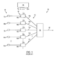
- an optical transmission system 100 includes, for example, a plurality of silicon waveguides 110 a . . . 110 n , collectively shown as waveguides 110 , each carrying data of an optical communications channel.
- the system 100 includes multiple data input channels 120 a . . . 120 n , collectively shown as 120 , where each data input channel 120 a . . . 120 n transmits data in the form of pulses of light or as electrical signals.
- each data input channel 120 a . . . 120 n transmits data in the form of pulses of light or as electrical signals.
- each data input channel 120 a . . . 120 n is modulated onto a respective optical carrier having a wavelength ⁇ 1 . . . ⁇ n , by a respective resonant optical modulator 130 a . . . 130 n .
- the outputs of the modulators 130 a . . . 130 n form respective optical communicating channels.
- the resonant optical modulators 130 a . . . 130 n are collectively shown as 130 .
- the optical carriers at wavelengths ⁇ 1 . . . ⁇ n can be supplied to each resonant optical modulator 130 a . . . 130 n by a highly accurate temperature controlled laser source 136 .
- each resonant optical modulator 130 a . . . 130 n is provided to a respective waveguide 110 a . . . 110 n and the outputs from the waveguides 110 are then multiplexed into a single optical transmission channel waveguide 150 by an optical multiplexer 140 .
- the multiplexed light is then transmitted along the waveguide 150 to an endpoint (not shown) where the data modulated light is de-multiplexed and demodulated before being used by an endpoint device.
- the resonant optical modulators 130 a . . . 130 n which may be ring modulators, are designed to resonate at their respective carrier wavelengths ⁇ 1 . . . ⁇ n .
- the resonant optical modulators 130 a . . . 130 n have resonant cavities and are constructed of materials with refractive indices, both of which are affected by temperature changes.
- the changes in temperature of the resonant optical modulators 130 a . . . 130 n cause their respective resonant frequencies to change and move away from their respective carrier wavelengths ⁇ 1 . . . ⁇ n .
- FIG. 1 shows an example of a conventional a wave division multiplex transmission system
- FIG. 2 shows a wave division multiplexing and demultiplexing system in accordance with an example embodiment of the invention.
- FIG. 3A shows an example of a conventional WDM optical communications system channel structure
- FIG. 3B shows an example of a WDM optical communications system channel structure which may be used with the FIG. 2 embodiment
- FIG. 4 illustrates one example of how a temperature change affects modulators of the FIG. 2 embodiment
- FIG. 5 illustrates an example of a temperature detector which detects changes in resonance frequency and which can be used with the FIG. 2 embodiment
- FIG. 6A illustrates an example of another detector which detects changes in resonance frequency of a modulator and which can be used with the FIG. 2 embodiment;
- FIG. 6B illustrates an eye diagram illustrating operation of the FIG. 6A detector
- FIGS. 7A , 7 B and 7 C show respective example embodiments of alternative demodulators which may be used in the FIG. 2 embodiment.
- Example embodiments described herein provide a wave division multiplex (WDM) optical communication system having a plurality of optical communications channels which can be multiplexed and demultiplexed.
- the WDM optical communications system can be partially or entirely integrated onto a die.
- Each optical communication channel has at least two spaced carriers and a data modulator having at least a first and a second resonant optical modulator circuit, each associated with a respective carrier.
- the first resonant optical modulator circuit has a resonant frequency at its respective carrier wavelength and the second resonant modulator circuit has a resonant frequency which is offset from its respective carrier wavelength.
- a detector which detects when the first modulator circuit is sufficiently out of resonance with its respective carrier wavelength and the second modulator circuit is in sufficient resonance with its respective carrier wavelength is used to control switching of data modulation from the first to the second modulator circuit. As a consequence, data for a given optical communication channel is switched to a different channel carrier wavelength where it is reliably modulated by the second modulator circuit.
- embodiments described and illustrated herein employ two modulator circuits and associated carrier wavelengths per optical communications channel, this is merely an example as more than two resonant modulator circuits, each having a respective carrier wavelength can be used for each optical communications channel.
- embodiments are described with reference to a temperature change causing changes in the resonant frequency of modulator circuits, the embodiments are not limited to being responsive to only temperature changes. The embodiments can also be used in any environment where there is an induced change in the resonant frequency of modulator circuits.
- the switch from the first resonant optical modulator circuit and respective carrier wavelength to the second resonant optical modulator circuit and respective carrier wavelength for transmitting data on an optical communication channel on the multiplex side can be communicated through an existing optical communications channel, or a separate electrical communications channel, to a demultiplexing side of the system.
- the demultiplexing side of the system uses the switching information to switch to the new modulated carrier wavelength and to an associated demodulator for proper data demodulation for each optical communications channel.
- the switching information is transmitted to the demultiplexing side prior to switching from the first to the second resonant optical modulator circuit on the multiplexing side so the demodulators can switch in synchronism with the switching of the modulator circuits.
- FIG. 2 illustrates the multiplexing 10 and demultiplexing 12 sides of a WDM system in an example embodiment.
- the multiplex side 10 includes a laser source 101 providing at least two carrier wavelengths to each resonant optical modulator 170 a . . . 170 n .
- Each of the resonant optical modulators 170 a . . . 170 n contain at least two distinct first and second optical modulator circuits.
- each resonant optical modulator 170 a these are optical modulator circuits 104 , 104 a; for optical modulator circuit 170 b , these are optical modulator circuits 108 , 108 a; for resonant optical modulator 170 n , these are optical modulator circuits 113 , 113 a .
- Each resonant optical modulator 170 a . . . 170 n output is a respective optical communications channel which is supplied to respective waveguides 110 a . . . 110 n .
- Each optical modulator 170 a . . . 170 n also receives respective data input as DATA 1, DATA2 . . .
- DATAN which can be supplied to each of the first and second optical modulator circuits within a given modulator 170 a . . . 170 n .
- the outputs of the resonant optical modulators 170 a . . . 170 n are supplied via respective waveguides 110 a . . . 110 n to an optical multiplexer 140 which multiplexes the optical communication channels on waveguides 110 onto a waveguide 142 which sends the multiplexed optical communications channels to the demultiplexing side 12 of the system.
- the demultiplexing side 12 includes optical demultiplexer 147 for demultiplexing the signals on waveguide 142 , a plurality of waveguides 172 a . . . 172 n for the respective ones of demultiplexed optical communications channels, and a plurality of demodulation circuits 109 a . . . 109 n for respectively demodulating the received carrier on waveguides 172 a . . . 172 n to supply demodulated data as DATA 1 (OUT) . . . DATAN (OUT).
- FIG. 3A shows an example of an optical communications channel carrier spacing in a conventional WDM system.
- Each of the optical communications channels are illustrated as having respective spaced wavelengths 115 of ⁇ 1 , ⁇ 2 , . . . ⁇ n which can be modulated.
- at least one additional carrier 117 is added for each optical communications channel.
- the additional carriers are offset from respective FIG. 3A carrier wavelengths and are shown in FIG. 3B as wavelengths ⁇ 1 ′, ⁇ 2 ′ . . . ⁇ n ′.
- at least two carriers 115 , 117 are available for data modulation for each optical communications channel on the multiplexing side 10 of the FIG. 2 system.
- laser source 101 is temperature controlled to provide stable carrier wavelengths and may be formed of one or more temperature controlled lasers.
- Laser source 101 provides the at least two carrier wavelengths shown in FIG. 3B , for each optical communications channel.
- the optical communications channel which is associated with modulator 170 a has two carriers at respective wavelengths ⁇ 1 and ⁇ 1 ′ provided to modulator 170 a .
- the same is true for each of the other optical communications channels associated with modulators 170 b . . . 170 n .
- laser source 101 is shown as having a respective waveguide connection to each of the modulators 170 a . . .
- a modulator 170 a . . . 170 n will only resonant with and modulate data onto a respective one of the at least two carrier wavelengths of its associated optical communications channel.
- each modulator 170 a . . . 170 n includes at least a first and second ring resonator optical modulation circuit, which are designed to resonate with only one of the two carriers provided for its associated optical communications channel.
- modulator 170 a contains optical modulation circuits 104 and 104 a each designed to be resonant with one of the two supplied carriers, e.g. ⁇ 1 (for 104 ) and ⁇ 1 ′ (for 104 a ).
- modulator 170 b contains resonant circuits 108 , 108 a associated with carriers ⁇ 2 (for 108 ) and ⁇ 2 ′ (for 108 a ), and modulator 170 n contains resonant circuits 113 , 113 a respectively associated with carriers ⁇ n , (for 113 ) and ⁇ n ′ (for 113 a ).
- the resonant frequencies of the two modulator circuits in each of modulators 170 a . . . 170 n are such that when a first of the two resonant circuits, e.g.
- the other resonant circuit 104 a is not resonant with its respective carrier ⁇ 1 ′ because the resonant frequency of the second modulator circuit 104 a is shifted away from its associated carrier ⁇ 40 ′.
- ring modulator circuit 104 has a resonant frequency ⁇ 1a which aligns well with the channel carrier wavelength ⁇ 1 . Accordingly, ring modulator circuit 104 can reliably transmit data denoted as DATA1 onto the carrier wavelength ⁇ 1 .
- each of the ring modulators 104 , 104 a has a respective driver circuit 106 , 106 a ( FIG. 2 ) which is selectively enabled by a switch command on control line 111 , such that only one ring modulator 104 , 104 a is active at a time.
- the resonant frequency of the ring modulator 104 shifts to a resonant frequency at a wavelength ⁇ 1b .
- modulator 104 can still resonate with its respective carrier a ⁇ 1 , but begins to lose its ability to resonate with the carrier ⁇ 1 .
- the first ring modulator circuit 104 loses its ability to reliably modulate data on its respective carrier ⁇ 1 while the second ring modulator 104 a is still able to resonate with and reliably modulate data onto its carrier ⁇ 1 ′.
- the bottom chart on FIG. 4 summarizes the operational states of ring modulators 104 , 104 a with respect to their ability to resonate with and modulate data on their respective carriers ⁇ 1 and ⁇ 1 ′ under the various temperature conditions.
- the ring modulator 104 will be turned off and ring modulator 104 a turned on so that only the latter now modulates incoming data (DATA1) onto its respective carrier ⁇ 1 ′.
- the switch point is a predetermined temperature where a first 104 of the two modulator circuits 104 , 104 a is instructed to stop modulating its respective carrier ⁇ 1 with data and the second modulator circuit 104 a is instructed to start modulating its respective carrier ⁇ 1 ′ with data.
- This predetermined temperature switch point may be applied globally such that when the switch point temperature is detected all of the ring modulators 170 a . . . 170 n each will simultaneously shift from their first to their second modulator circuit. Since modulators 170 a . . . 170 n can be provided on a common integrated circuit die, a die temperature detector can be commonly used to determine a switch point for all modulators 170 a . . . 170 n .
- the switch command is commonly applied to all modulators 170 a . . . 170 n by a control line 111 .
- FIG. 5 illustrates a temperature detector circuit which can be used to determine when the switch point is reached and issue a corresponding switch command on control line 111 ( FIG. 2 ) to modulators 170 a . . . 170 n .
- It includes a temperature sensor 133 , such as a thermistor, which has an output connected to one input of a comparator 134 .
- Another input to comparator 134 provides a threshold reference value which must be exceeded for comparator 134 to switch the value of an output signal. This reference value may be selected to correspond to the predetermined temperature which must be reached for the switch command to be issued.
- FIG. 5 illustrates a temperature detector circuit which can be used to determine when the switch point is reached and issue a corresponding switch command on control line 111 ( FIG. 2 ) to modulators 170 a . . . 170 n .
- It includes a temperature sensor 133 , such as a thermistor, which has an output connected to one input of a comparator 134
- a hysteresis circuit 127 in the form of a Schmitt Trigger which provides the switch command signal on control line 111 to control a shift from the first ring modulator circuit to the second for all of the modulators 170 a . . . 170 n.
- each of the ring modulator circuits within a modulator 170 a . . . 170 n includes an associated driver circuit 106 , 106 a; 107 , 107 a; 115 , 115 a , for driving the first and second modulator circuit of each modulator 170 a . . . 170 n with respective input data, e.g. DATA1, . . . DATAN.
- the driver circuits respond to the switch command signal from the FIG. 5 circuit on control line 111 to control the switch from the first modulator circuit to the second for the modulators 170 a . . . 170 n .
- the driver circuits 106 , 106 a control the switch from first modulator circuit 104 to the second modulator circuit 104 a , for the modulator 170 a .
- the driver circuits 106 , 106 a have an enable/disable input line which receives the switch command from control line 111 .
- the driver circuits, e.g. 106 , 106 a can be electrical circuits receiving electrical data input or optical circuits receiving optical data input.
- a logic value of “1” or “0” can be supplied by Schmitt Trigger 127 on control line 111 as the switch command.
- the switch command also needs to be communicated to the demodulation circuits on the demultiplexing side 12 of the FIG. 2 system so that demodulators which are demodulating a particular carrier, e.g. ⁇ 1 , ⁇ 1 ′ for an optical communications channel know which channel carrier to demodulate.
- the switch command can be sent on a particular optical data channel on the multiplexing side 10 to the demultiplexing side 12 .
- the FIG. 2 embodiment shows the modulator 170 n being used for this purpose as the wavelength switch command can be part of the input DATAN, although any optical data channel can be used.
- a separate electrical channel can be used to transmit the switch command from the multiplexing side 10 to the demultiplexing side 12 .
- the switch command is sent before an actual switch from the first to the second modulator circuit within the modulators 170 a . . . 170 n occurs on the multiplexing side 10 so the demodulators know when to switch and can switch in synchronism with the modulators 170 a . . . 170 n.
- FIGS. 6A and 6B show another arrangement for providing a switch command signal on control line 111 .
- FIG. 6A shows an alternative modulator 170 a ′ having respective modulator circuits 104 , 104 a and associated driver circuits 106 , 106 a .
- a light tap 124 , 124 a can be provided in association with the output of a respective modulator circuit 104 , 104 a to receive a small portion of modulated light representing the light output by the respective modulator circuits 104 , 104 a .
- the light taps 124 , 124 a connect with respective photo detectors 125 , 125 a .
- FIG. 6B shows an eye diagram representing the modulation index of a modulation circuit.
- Comparator 125 can be used to determine when the lowered modulation index is achieved, for example, a modulation index lowered by 8 dB, and provide a switch signal indicating that a switch should occur from the first modulation circuit 104 to the second 104 a .
- a hysteresis circuit 127 such as a Schmitt Trigger, provides the switch control signal.
- FIG. 6A also shows a separate detector, which includes tap 124 a , photo detector 125 a , comparator 126 a , a Schmitt Trigger and hysteresis circuit 127 a , for detecting loss of resonance of the second modulator circuit 104 a ′ with its respective carrier ⁇ 1 ′. This is used to determine when the temperature of the modulators 170 a . . . 170 n has lowered to the point where a switch should occur from the second modulator circuit 104 a modulating its carrier ⁇ 1 ′ back to the first modulator circuit 104 for modulating its carrier ⁇ 1 .
- the FIG. 5 temperature detector output can also be used to switch back from the second 104 a to the first 104 modulator circuit when the detected temperature falls below the switch threshold set by comparator 134 .
- the carriers of optical communications channels are demultiplexed by demultiplexer 147 and the demultiplexed optical communications channels are provided on respective waveguides 172 a . . . 172 n .
- Each of the demultiplexed optical communications channels can have data modulated on one of at least two carriers of the communications channel, e.g. ⁇ 1 , or ⁇ 1 ′ for the optical communications channel associated with modulator 170 a on the multiplex side 10 .
- Each optical communications channel on respective waveguides 172 a . . . 172 n has an associated demodulator 109 a . . .
- demodulator 109 a each of which contains at least a first and second wide band resonant ring demodulator circuit.
- demodulator 109 a includes first and second resonant ring demodulator circuits 200 , 200 a for respectively demodulating the carriers ⁇ 1 , ⁇ 1 ′.
- demodulators 109 b and 109 n have demodulator circuits 201 , 201 a and 205 , 205 a respectively.
- Each of the demodulator circuits, 200 , 200 a; 201 , 201 a; 205 , 205 a are wide band resonant ring demodulator circuits which are capable of resonating with and demodulating a respective carrier over wide ranges of temperature changes, which otherwise would adversely affect a modulating circuit, e.g. 104 , 104 a.
- the switch command generated on the multiplexer side 10 and sent to the demultiplexer side 12 tells the demodulators 109 a . . . 109 n which internal demodulation circuit to use corresponding to the carrier wavelength which is being modulated for the corresponding optical communications channel.
- a shift from a first demodulator circuit, e.g. 200 to second, e.g. 200 a occurs within a demodulator 109 a . . . 109 n
- the switch command is received, demodulated off the communications channel communicating it, e.g. demodulator 109 n , and sent on control line 113 to all of the demodulators 109 a . . .
- Each demodulator circuit, e.g. 200 , 200 a has an associated light tap for receiving demodulated data and passing it to a respective photo detector e.g. 123 , 123 a for demodulator 109 a , 223 , 223 a for demodulator 109 b , and 323 , 323 a for demodulator 109 n .
- the respective photo detectors 123 , 123 a , 223 , 223 a , 323 , 323 a can be turned on or off by the received switch command on control line 113 such that only one photo detector of each pair is on at a time.
- one logic state of a switch command e.g. “1” can be used to turn on a first photo detector, e.g. 123 while turning off a second photo detector e.g. 123 a .
- the other logic state e.g. “0”
- Each of the demodulators 109 a . . . 109 n has the output of the photo detector e.g. 123 , 123 a combined to provide a data output signal, e.g. DATA 1 (Out) for demodulator 109 a .
- one of the demodulator circuits e.g. 200 , 200 a which demodulates its associated channel carrier ⁇ 1 , ⁇ 1 ′, is selected for providing a data output signal e.g. DATA 1 (Out) for its associated optical communications channel.
- FIG. 7A illustrates a modified demodulator 109 ′ which can be used in the FIG. 2 system in place of the demodulators 109 a . . . 109 n .
- the photo detector outputs remain separate.
- the switch command on line 113 is used to select one or the other of photo detectors 135 , 135 a for output.
- FIG. 7B illustrates another demodulator 109 ′′ which can be used in the FIG. 2 system in place of the demodulators 109 a . . . 109 n .
- each demodulator circuit within demodulator 109 ′′ is formed by pair of narrow band ring demodulators 220 , 222 and 220 a , 222 a .
- the first pair of ring demodulators, e.g. 220 , 222 have resonant frequencies slightly offset from one another, with one being centered on the first carrier of a optical communications channel and the other offset from that.
- demodulator circuit 222 moves into closer resonance with the first carrier ⁇ 1 .
- the output of both ring demodulators 220 and 222 are optically combined and fed to a single photo detector 137 which provides a data output signal, e.g. DATA1(OUT).
- a second demodulation circuit is also included within demodulator 109 ′′ and is formed by a second pair of narrow band ring demodulators 220 a , 222 a . They are arranged such that one of the ring demodulators 220 a has a resonant frequency which is centered on the second carrier wavelength of a communication channel, e.g. ⁇ 1 ′ for the optical communications channel associated with modulator 170 a and with the other ring demodulator 220 b slightly offset from that.
- the optical communications channel is using the second carrier ⁇ 1 ′, and there is temperature change which moves resonance of demodulator circuit 220 a away from the carrier ⁇ 1 ′, the demodulator circuit 222 a moves into resonance with carrier ⁇ 1 ′, the outputs of both ring demodulators 220 a , 222 a are combined and sent to a photo detector 137 a .
- the received switch command on line 113 is used to select one of the photo detectors 137 , 137 a output for providing output data, e.g. DATA 1 (Out).
- FIG. 7C shows another demodulator 109 ′′′ which may be used in the FIG. 2 system.
- Demodulator 109 ′′′ is similar to demodulator 109 ′′. However, unlike in demodulator 109 ′′, where the optical outputs of the paired ring demodulators 220 , 222 and 220 a , 222 a are first optically combined and then sent to respective photodiodes 137 , 137 a , in demodulator 109 ′′′ the optical signals from the paired narrow band ring demodulators 220 , 222 and 220 a , 222 a are sent directly to the respective photo detectors 137 , 137 a.
Landscapes
- Engineering & Computer Science (AREA)
- Computer Networks & Wireless Communication (AREA)
- Signal Processing (AREA)
- Physics & Mathematics (AREA)
- Electromagnetism (AREA)
- Optical Communication System (AREA)
- Optical Modulation, Optical Deflection, Nonlinear Optics, Optical Demodulation, Optical Logic Elements (AREA)
- Semiconductor Lasers (AREA)
Abstract
Description
Claims (27)
Priority Applications (1)
| Application Number | Priority Date | Filing Date | Title |
|---|---|---|---|
| US14/220,316 US8861978B2 (en) | 2012-07-12 | 2014-03-20 | Method and apparatus providing wave division multiplexing optical communication system with active carrier hopping |
Applications Claiming Priority (2)
| Application Number | Priority Date | Filing Date | Title |
|---|---|---|---|
| US13/547,139 US8718466B2 (en) | 2012-07-12 | 2012-07-12 | Method and apparatus providing wave division multiplexing optical communication system with active carrier hopping |
| US14/220,316 US8861978B2 (en) | 2012-07-12 | 2014-03-20 | Method and apparatus providing wave division multiplexing optical communication system with active carrier hopping |
Related Parent Applications (1)
| Application Number | Title | Priority Date | Filing Date |
|---|---|---|---|
| US13/547,139 Continuation US8718466B2 (en) | 2012-07-12 | 2012-07-12 | Method and apparatus providing wave division multiplexing optical communication system with active carrier hopping |
Publications (2)
| Publication Number | Publication Date |
|---|---|
| US20140205289A1 US20140205289A1 (en) | 2014-07-24 |
| US8861978B2 true US8861978B2 (en) | 2014-10-14 |
Family
ID=48874482
Family Applications (2)
| Application Number | Title | Priority Date | Filing Date |
|---|---|---|---|
| US13/547,139 Active 2032-10-13 US8718466B2 (en) | 2012-07-12 | 2012-07-12 | Method and apparatus providing wave division multiplexing optical communication system with active carrier hopping |
| US14/220,316 Active US8861978B2 (en) | 2012-07-12 | 2014-03-20 | Method and apparatus providing wave division multiplexing optical communication system with active carrier hopping |
Family Applications Before (1)
| Application Number | Title | Priority Date | Filing Date |
|---|---|---|---|
| US13/547,139 Active 2032-10-13 US8718466B2 (en) | 2012-07-12 | 2012-07-12 | Method and apparatus providing wave division multiplexing optical communication system with active carrier hopping |
Country Status (8)
| Country | Link |
|---|---|
| US (2) | US8718466B2 (en) |
| EP (1) | EP2873176B1 (en) |
| JP (1) | JP6010696B2 (en) |
| KR (2) | KR101665272B1 (en) |
| CN (2) | CN104541463B (en) |
| SG (1) | SG11201500153PA (en) |
| TW (1) | TWI516041B (en) |
| WO (1) | WO2014011396A1 (en) |
Cited By (1)
| Publication number | Priority date | Publication date | Assignee | Title |
|---|---|---|---|---|
| US10890718B2 (en) | 2018-11-21 | 2021-01-12 | Centera Photonics Inc. | Silicon photonic integrated system in a switch |
Families Citing this family (11)
| Publication number | Priority date | Publication date | Assignee | Title |
|---|---|---|---|---|
| KR20130093839A (en) * | 2012-01-26 | 2013-08-23 | 삼성전자주식회사 | Optical transmitters and optical communication systems using thermal coupled resonance modulator |
| JP6266311B2 (en) * | 2013-11-08 | 2018-01-24 | 富士通株式会社 | Optical resonator, optical transmitter and optical resonator control method |
| US9494736B2 (en) * | 2014-06-27 | 2016-11-15 | Intel Corporation | Technologies for generating a broadband optical output |
| JP6427992B2 (en) * | 2014-06-30 | 2018-11-28 | 富士通株式会社 | Optical transmission system, transmitter, receiver, and optical transmission method |
| EP3207649A4 (en) * | 2014-10-14 | 2018-07-11 | The Arizona Board of Regents on behalf of the University of Arizona | Multi-wavelength balanced optical transmission networks |
| US10009135B2 (en) * | 2015-02-06 | 2018-06-26 | The Trustees Of Princeton University | System and method for photonic processing |
| EP3271773B1 (en) * | 2015-07-21 | 2022-04-20 | Hewlett Packard Enterprise Development LP | Ring-resonator modulation of an optical signal |
| US10429676B2 (en) * | 2015-07-23 | 2019-10-01 | Hewlett Packard Enterprise Development Lp | Ring waveguide modulators |
| US11233577B1 (en) * | 2020-09-03 | 2022-01-25 | Hewlett Packard Enterprise Development Lp | Optical communication systems and methods to communicate temperature variation information |
| US11201686B1 (en) * | 2020-09-15 | 2021-12-14 | International Business Machines Corporation | Optically multiplexed quantum control |
| US11460877B2 (en) | 2020-12-12 | 2022-10-04 | Anyon Systems Inc. | Hybrid photonics-solid state quantum computer |
Citations (14)
| Publication number | Priority date | Publication date | Assignee | Title |
|---|---|---|---|---|
| JPS5510250A (en) | 1978-07-10 | 1980-01-24 | Anritsu Corp | Lc oscillator |
| US5760937A (en) | 1994-08-02 | 1998-06-02 | Fujitsu Limited | Optical demultiplexer |
| US20020081055A1 (en) | 1998-11-13 | 2002-06-27 | Painter Oskar J. | Resonant optical modulators |
| US20020176132A1 (en) | 2001-05-25 | 2002-11-28 | Mohsen Sarraf | Differential dense wavelength division multiplexing (DDWDM) in optical systems |
| US20030012250A1 (en) | 2001-06-25 | 2003-01-16 | Masataka Shirasaki | Tunable filter for laser wavelength selection |
| US20030025966A1 (en) | 2001-08-03 | 2003-02-06 | Ross Halgren | OSP hardened WDM network |
| US20030026529A1 (en) | 2001-08-06 | 2003-02-06 | Durkin Michael Kevan | Optical demultiplexer |
| KR20040057477A (en) | 2002-12-26 | 2004-07-02 | 엘지이노텍 주식회사 | Sensing system using surface acoustic wave resonator |
| US6888681B2 (en) | 2002-01-31 | 2005-05-03 | Nippon Sheet Glass Co., Ltd. | Optical demultiplexer |
| US20060177221A1 (en) | 2003-01-28 | 2006-08-10 | Marconi Communitions Gmbh | Transmitter and method for transmitting messages on an optical fiber |
| EP1793513A2 (en) | 2005-11-30 | 2007-06-06 | Fujitsu Ltd. | Optical transmission apparatus |
| US7800282B2 (en) | 2007-09-19 | 2010-09-21 | Integrated Device Technology, Inc. | Single-resonator dual-frequency lateral-extension mode piezoelectric oscillators, and operating methods thereof |
| US20100329685A1 (en) | 2009-06-29 | 2010-12-30 | Sun Microsystems, Inc. | Optical device with reduced thermal tuning energy |
| US20110280579A1 (en) | 2010-05-11 | 2011-11-17 | Mclaren Moray | Energy-efficient and fault-tolerant resonator-based modulation and wavelength division multiplexing systems |
Family Cites Families (11)
| Publication number | Priority date | Publication date | Assignee | Title |
|---|---|---|---|---|
| KR19980067126U (en) * | 1997-05-23 | 1998-12-05 | 윤종용 | Drive control unit of cooling fan motor |
| CN1336044A (en) * | 1998-12-23 | 2002-02-13 | 艾利森电话股份有限公司 | Multi-transmitter system |
| US20030165173A1 (en) * | 2002-03-01 | 2003-09-04 | Helbing Rene P. | Multiple modulated wavelengths in a compact laser |
| JP4173392B2 (en) * | 2003-03-20 | 2008-10-29 | 株式会社日立製作所 | Optical transmitter |
| US8032027B2 (en) * | 2005-07-25 | 2011-10-04 | Massachusetts Institute Of Technology | Wide free-spectral-range, widely tunable and hitless-switchable optical channel add-drop filters |
| CN2834033Y (en) * | 2005-09-30 | 2006-11-01 | 中国科学院长春光学精密机械与物理研究所 | Wave guide optional wavelength wave division multiplexer/demultiplexer |
| US7257283B1 (en) * | 2006-06-30 | 2007-08-14 | Intel Corporation | Transmitter-receiver with integrated modulator array and hybrid bonded multi-wavelength laser array |
| JP2008270583A (en) * | 2007-04-23 | 2008-11-06 | Nec Corp | Wavelength variable light source and its control method, and program for control |
| CN102349013B (en) * | 2009-01-09 | 2014-04-16 | 惠普开发有限公司 | Optical engine for point-to-point communications |
| WO2010087790A1 (en) * | 2009-01-27 | 2010-08-05 | Hewlett-Packard Development Company, L.P. | Redundant ring resonators of varying dimensions to reduce ring resonator tuning requirements |
| WO2010108093A2 (en) * | 2009-03-20 | 2010-09-23 | Cornell University | Apparatus and methods for wide temperature range operation of micrometer-scale silicon electro-optic modulators |
-
2012
- 2012-07-12 US US13/547,139 patent/US8718466B2/en active Active
-
2013
- 2013-06-26 CN CN201380042257.7A patent/CN104541463B/en active Active
- 2013-06-26 JP JP2015521640A patent/JP6010696B2/en active Active
- 2013-06-26 EP EP13740405.9A patent/EP2873176B1/en active Active
- 2013-06-26 CN CN201710063397.2A patent/CN106850074B/en active Active
- 2013-06-26 WO PCT/US2013/047875 patent/WO2014011396A1/en active Application Filing
- 2013-06-26 KR KR1020157003583A patent/KR101665272B1/en active IP Right Grant
- 2013-06-26 SG SG11201500153PA patent/SG11201500153PA/en unknown
- 2013-06-26 KR KR1020167027504A patent/KR101961533B1/en active IP Right Grant
- 2013-07-08 TW TW102124401A patent/TWI516041B/en active
-
2014
- 2014-03-20 US US14/220,316 patent/US8861978B2/en active Active
Patent Citations (14)
| Publication number | Priority date | Publication date | Assignee | Title |
|---|---|---|---|---|
| JPS5510250A (en) | 1978-07-10 | 1980-01-24 | Anritsu Corp | Lc oscillator |
| US5760937A (en) | 1994-08-02 | 1998-06-02 | Fujitsu Limited | Optical demultiplexer |
| US20020081055A1 (en) | 1998-11-13 | 2002-06-27 | Painter Oskar J. | Resonant optical modulators |
| US20020176132A1 (en) | 2001-05-25 | 2002-11-28 | Mohsen Sarraf | Differential dense wavelength division multiplexing (DDWDM) in optical systems |
| US20030012250A1 (en) | 2001-06-25 | 2003-01-16 | Masataka Shirasaki | Tunable filter for laser wavelength selection |
| US20030025966A1 (en) | 2001-08-03 | 2003-02-06 | Ross Halgren | OSP hardened WDM network |
| US20030026529A1 (en) | 2001-08-06 | 2003-02-06 | Durkin Michael Kevan | Optical demultiplexer |
| US6888681B2 (en) | 2002-01-31 | 2005-05-03 | Nippon Sheet Glass Co., Ltd. | Optical demultiplexer |
| KR20040057477A (en) | 2002-12-26 | 2004-07-02 | 엘지이노텍 주식회사 | Sensing system using surface acoustic wave resonator |
| US20060177221A1 (en) | 2003-01-28 | 2006-08-10 | Marconi Communitions Gmbh | Transmitter and method for transmitting messages on an optical fiber |
| EP1793513A2 (en) | 2005-11-30 | 2007-06-06 | Fujitsu Ltd. | Optical transmission apparatus |
| US7800282B2 (en) | 2007-09-19 | 2010-09-21 | Integrated Device Technology, Inc. | Single-resonator dual-frequency lateral-extension mode piezoelectric oscillators, and operating methods thereof |
| US20100329685A1 (en) | 2009-06-29 | 2010-12-30 | Sun Microsystems, Inc. | Optical device with reduced thermal tuning energy |
| US20110280579A1 (en) | 2010-05-11 | 2011-11-17 | Mclaren Moray | Energy-efficient and fault-tolerant resonator-based modulation and wavelength division multiplexing systems |
Non-Patent Citations (6)
| Title |
|---|
| A. Biberman et al., "Broadband Silicon Photonic Electrooptic Switch for Photonic Interconnection Networks," IEEE Photonics Technology Letters, vol. 23, No. 8, pp. 504-506, Apr. 15, 2011. |
| B. T. Smith et al., Integrated Silicon Photonic Circuit: Monolithic 8-Channel Modulator, Tap, Vertical Coupler, and Flip-Chip Mounted Photodetector Array, Kotura, Inc., Monterey Park, CA, Proc. SPIE Silicon Photonics, Mar. 2006. |
| Eye Pattern-Wikipedia, the free Encyclopedia, http://en.wikipedia.org/wiki/Eye-pattern, Apr. 24, 2012. |
| L. Chen et al., "Integrated GHz Silicon Photonic Interconnect with Micrometer-Scale Modulators and Detectors". Optics Express, vol. 17, No. 17, pp. 15248-15256, Aug. 17, 2009. |
| Network Tap, Wikipedia, the free Encyclopedia, http://en.wikipedia.org/wiki/Network-tap, Apr. 25, 2012. |
| R. Amatya et al., "Efficient Thermal Tuning for Second-Order Silicon Nitride Microring Resonators," IEEE Research Laboratory of Electronics (RLE), Massachusetts Institute of Technology, pp. 149-150, 2007. |
Cited By (1)
| Publication number | Priority date | Publication date | Assignee | Title |
|---|---|---|---|---|
| US10890718B2 (en) | 2018-11-21 | 2021-01-12 | Centera Photonics Inc. | Silicon photonic integrated system in a switch |
Also Published As
| Publication number | Publication date |
|---|---|
| JP6010696B2 (en) | 2016-10-19 |
| WO2014011396A1 (en) | 2014-01-16 |
| SG11201500153PA (en) | 2015-02-27 |
| CN104541463B (en) | 2017-03-01 |
| US8718466B2 (en) | 2014-05-06 |
| KR101961533B1 (en) | 2019-07-17 |
| TW201412042A (en) | 2014-03-16 |
| CN106850074A (en) | 2017-06-13 |
| EP2873176A1 (en) | 2015-05-20 |
| KR20160119877A (en) | 2016-10-14 |
| TWI516041B (en) | 2016-01-01 |
| CN104541463A (en) | 2015-04-22 |
| US20140016931A1 (en) | 2014-01-16 |
| EP2873176B1 (en) | 2017-10-04 |
| JP2015534291A (en) | 2015-11-26 |
| CN106850074B (en) | 2020-10-27 |
| KR20150038044A (en) | 2015-04-08 |
| US20140205289A1 (en) | 2014-07-24 |
| KR101665272B1 (en) | 2016-10-11 |
Similar Documents
| Publication | Publication Date | Title |
|---|---|---|
| US8861978B2 (en) | Method and apparatus providing wave division multiplexing optical communication system with active carrier hopping | |
| US11777633B2 (en) | Optical multiplexer/demultiplexer module and associated methods | |
| US10142712B2 (en) | Photonic transceiver architecture with loopback functionality | |
| Doerr et al. | Single-chip silicon photonics 100-Gb/s coherent transceiver | |
| US10439727B2 (en) | Method and system for selectable parallel optical fiber and wavelength division multiplexed operation | |
| CN109791315B (en) | Method and system for vertical junction high speed phase modulator | |
| CN113810118B (en) | Single body integrated coherent transceiver | |
| US20150316793A1 (en) | Method and system for a low parasitic silicon high-speed phase modulator | |
| US20170155464A1 (en) | Optical wavelength automatic adaptation of transceivers | |
| US9185475B1 (en) | Signal quality in bi-directional optical links using optical circulators | |
| US9461770B2 (en) | Method and system for floating grid transceiver | |
| JP2008160719A (en) | Optical signal transmission apparatus | |
| KR102005285B1 (en) | Microring-based optical link apparatus | |
| KR20160011752A (en) | On-chip reconfigurable method of silicon-based optical transceiver and optical transmitting and receiving apparatus thereof |
Legal Events
| Date | Code | Title | Description |
|---|---|---|---|
| FEPP | Fee payment procedure |
Free format text: PAYOR NUMBER ASSIGNED (ORIGINAL EVENT CODE: ASPN); ENTITY STATUS OF PATENT OWNER: LARGE ENTITY |
|
| STCF | Information on status: patent grant |
Free format text: PATENTED CASE |
|
| CC | Certificate of correction | ||
| AS | Assignment |
Owner name: U.S. BANK NATIONAL ASSOCIATION, AS COLLATERAL AGENT, CALIFORNIA Free format text: SECURITY INTEREST;ASSIGNOR:MICRON TECHNOLOGY, INC.;REEL/FRAME:038669/0001 Effective date: 20160426 Owner name: U.S. BANK NATIONAL ASSOCIATION, AS COLLATERAL AGEN Free format text: SECURITY INTEREST;ASSIGNOR:MICRON TECHNOLOGY, INC.;REEL/FRAME:038669/0001 Effective date: 20160426 |
|
| AS | Assignment |
Owner name: MORGAN STANLEY SENIOR FUNDING, INC., AS COLLATERAL AGENT, MARYLAND Free format text: PATENT SECURITY AGREEMENT;ASSIGNOR:MICRON TECHNOLOGY, INC.;REEL/FRAME:038954/0001 Effective date: 20160426 Owner name: MORGAN STANLEY SENIOR FUNDING, INC., AS COLLATERAL Free format text: PATENT SECURITY AGREEMENT;ASSIGNOR:MICRON TECHNOLOGY, INC.;REEL/FRAME:038954/0001 Effective date: 20160426 |
|
| AS | Assignment |
Owner name: U.S. BANK NATIONAL ASSOCIATION, AS COLLATERAL AGENT, CALIFORNIA Free format text: CORRECTIVE ASSIGNMENT TO CORRECT THE REPLACE ERRONEOUSLY FILED PATENT #7358718 WITH THE CORRECT PATENT #7358178 PREVIOUSLY RECORDED ON REEL 038669 FRAME 0001. ASSIGNOR(S) HEREBY CONFIRMS THE SECURITY INTEREST;ASSIGNOR:MICRON TECHNOLOGY, INC.;REEL/FRAME:043079/0001 Effective date: 20160426 Owner name: U.S. BANK NATIONAL ASSOCIATION, AS COLLATERAL AGEN Free format text: CORRECTIVE ASSIGNMENT TO CORRECT THE REPLACE ERRONEOUSLY FILED PATENT #7358718 WITH THE CORRECT PATENT #7358178 PREVIOUSLY RECORDED ON REEL 038669 FRAME 0001. ASSIGNOR(S) HEREBY CONFIRMS THE SECURITY INTEREST;ASSIGNOR:MICRON TECHNOLOGY, INC.;REEL/FRAME:043079/0001 Effective date: 20160426 |
|
| MAFP | Maintenance fee payment |
Free format text: PAYMENT OF MAINTENANCE FEE, 4TH YEAR, LARGE ENTITY (ORIGINAL EVENT CODE: M1551) Year of fee payment: 4 |
|
| AS | Assignment |
Owner name: JPMORGAN CHASE BANK, N.A., AS COLLATERAL AGENT, ILLINOIS Free format text: SECURITY INTEREST;ASSIGNORS:MICRON TECHNOLOGY, INC.;MICRON SEMICONDUCTOR PRODUCTS, INC.;REEL/FRAME:047540/0001 Effective date: 20180703 Owner name: JPMORGAN CHASE BANK, N.A., AS COLLATERAL AGENT, IL Free format text: SECURITY INTEREST;ASSIGNORS:MICRON TECHNOLOGY, INC.;MICRON SEMICONDUCTOR PRODUCTS, INC.;REEL/FRAME:047540/0001 Effective date: 20180703 |
|
| AS | Assignment |
Owner name: MICRON TECHNOLOGY, INC., IDAHO Free format text: RELEASE BY SECURED PARTY;ASSIGNOR:U.S. BANK NATIONAL ASSOCIATION, AS COLLATERAL AGENT;REEL/FRAME:047243/0001 Effective date: 20180629 |
|
| AS | Assignment |
Owner name: MICRON TECHNOLOGY, INC., IDAHO Free format text: RELEASE BY SECURED PARTY;ASSIGNOR:MORGAN STANLEY SENIOR FUNDING, INC., AS COLLATERAL AGENT;REEL/FRAME:050937/0001 Effective date: 20190731 |
|
| AS | Assignment |
Owner name: MICRON SEMICONDUCTOR PRODUCTS, INC., IDAHO Free format text: RELEASE BY SECURED PARTY;ASSIGNOR:JPMORGAN CHASE BANK, N.A., AS COLLATERAL AGENT;REEL/FRAME:051028/0001 Effective date: 20190731 Owner name: MICRON TECHNOLOGY, INC., IDAHO Free format text: RELEASE BY SECURED PARTY;ASSIGNOR:JPMORGAN CHASE BANK, N.A., AS COLLATERAL AGENT;REEL/FRAME:051028/0001 Effective date: 20190731 |
|
| MAFP | Maintenance fee payment |
Free format text: PAYMENT OF MAINTENANCE FEE, 8TH YEAR, LARGE ENTITY (ORIGINAL EVENT CODE: M1552); ENTITY STATUS OF PATENT OWNER: LARGE ENTITY Year of fee payment: 8 |