US8856715B1 - Capacitor designs for integrated circuits utilizing self-aligned double patterning (SADP) - Google Patents
Capacitor designs for integrated circuits utilizing self-aligned double patterning (SADP) Download PDFInfo
- Publication number
- US8856715B1 US8856715B1 US13/948,249 US201313948249A US8856715B1 US 8856715 B1 US8856715 B1 US 8856715B1 US 201313948249 A US201313948249 A US 201313948249A US 8856715 B1 US8856715 B1 US 8856715B1
- Authority
- US
- United States
- Prior art keywords
- routes
- vertical
- route
- providing
- mandrel
- Prior art date
- Legal status (The legal status is an assumption and is not a legal conclusion. Google has not performed a legal analysis and makes no representation as to the accuracy of the status listed.)
- Expired - Fee Related
Links
Images


Classifications
-
- G06F17/5072—
-
- G—PHYSICS
- G06—COMPUTING; CALCULATING OR COUNTING
- G06F—ELECTRIC DIGITAL DATA PROCESSING
- G06F30/00—Computer-aided design [CAD]
- G06F30/30—Circuit design
- G06F30/39—Circuit design at the physical level
- G06F30/394—Routing
Definitions
- the present disclosure relates to manufacture of semiconductor devices.
- the present disclosure is particularly applicable for integrating back-end of line (BEoL) vertical natural capacitors (VNCAPs) into integrated circuits (ICs) utilizing SADP technology.
- BEoL back-end of line
- VNCAPs vertical natural capacitors
- BEoL VNCAPs In fabrication of semiconductor devices, BEoL VNCAPs frequently offer higher capacitance density and lower cost over other technologies such as metal-insulator-metal (MIM) planar capacitors.
- MIM metal-insulator-metal
- BEoL VNCAP designs utilized litho-etch (LE) processes for a 45 to 90 nanometer (nm) technology node.
- BEoL VNCAP designs utilized litho-etch-litho-etch (LELE) processes for a 45-28 nm technology node.
- LELELE litho-etch-litho-etch-litho-etch
- An aspect of the present disclosure is a method of enabling integration of capacitor components in an IC by, inter alia, providing a set of routes (e.g., patterns) in mandrel recesses connected to a first vertical segment (e.g., strap) and separated from a second vertical segment (e.g., strap).
- routes e.g., patterns
- Another aspect of the present disclosure is a device having, inter alia, a plurality of third routes (e.g., floating fingers) separated from first and second nets, each of the third routes extending horizontally on one of equally spaced vertical positions and separating one route of a first net from one route of a second net (e.g., interdigitated).
- third routes e.g., floating fingers
- some technical effects may be achieved in part by a method including: providing a plurality of mandrel recesses extending horizontally on a substrate, each of the mandrel recesses having an identical width and being separated from another one of the mandrel recesses by an identical distance; providing a plurality of routes, each of the plurality of routes being positioned in a different one of the mandrel recesses; and providing first and second vertical segments on the substrate, the first vertical segment being connected to a set of the plurality of routes and separated from the second vertical segment, and the second vertical segment being separated from the set of routes.
- aspects include providing a plurality of second routes in a plurality of non-mandrel recesses extending horizontally on the substrate and separated from the first vertical segment, each of the non-mandrel recesses being positioned on a midpoint between two adjacent mandrel recesses of the mandrel recesses and having the identical width. Additional aspects include: providing the second routes abutting the second vertical segment and separated from the first set of routes; and providing the second vertical segment in a non-mandrel region.
- Some aspects include: providing a mandrel region partially surrounding the second vertical segment; providing a block mask over the mandrel region, the block mask being separated from the second vertical segment; and etching, after providing the block mask, the block mask preventing etching of a covered portion of the mandrel region. Further aspects include: providing the second vertical segment in a mandrel region and abutting a second set of the first routes, each route of the second set being separated from a route of the first set by one route of the second routes; and providing the second routes separated from the second vertical segment.
- Additional aspects include: providing a mandrel region including first and second vertical portions overlapping the first and second vertical segments, respectively, and a plurality of horizontal portions overlapping the mandrel recesses, each of the horizontal portions abutting the first and second vertical segments, having a width equal to the identical width, and being separated from another one of the horizontal portions the identical distance; providing a block mask including a plurality of alternating third and fourth vertical portions on the horizontal portions, the third and fourth vertical portions abutting the second and first vertical segments, respectively; and etching, after providing the block mask, the block mask preventing etching of a covered portion of the mandrel region.
- Some aspects include a method, wherein the second vertical segment is connected to a second set of the first routes and separated from routes of the first set, the method further including: providing a mandrel region including first and second vertical portions overlapping the first and second vertical segments, respectively, and a plurality of first horizontal portions overlapping the mandrel recesses, each of the first horizontal portions extending a separation distance between the first and second vertical portions, abutting the first and second vertical portions, having a width equal to the identical width, and separated from another one of the first horizontal portions by the identical distance; providing a block mask including: a plurality of alternating third and fourth vertical portions on the first horizontal portions, the third and fourth vertical portions abutting the second and first vertical segments, respectively; and a plurality of second horizontal portions extending horizontally an entire distance separating the first and second vertical segments, each of the second horizontal portions separating one of the first horizontal segments from one of the third or fourth vertical portions; and etching, after providing the block mask, the block mask preventing etching of a
- Additional aspects include: providing the plurality of first routes and the first and second vertical segments in a first level of the substrate; and providing a plurality of third and fourth routes in a second level of the substrate, the third routes being connected to the first routes, and the fourth routes being separated from the first routes, wherein each route of the third and fourth routes extends in a direction perpendicular to each route of the first routes, or each route of the third and fourth routes extends in a direction parallel to each route of the first routes.
- Another aspect of the present disclosure is a device including: a first net including a plurality of first routes, each of the first routes extending horizontally on one vertical position of a plurality of equally spaced vertical positions on a substrate; a second net including a plurality of second routes, each of the second routes extending horizontally on one of the vertical positions, the first and second nets being separated; and a plurality of third routes separated from the first and second nets, each of the third routes extending horizontally on one of the vertical positions and separating one of the first routes from one of the second routes.
- Some aspects include: the first net further including a fourth route extending vertically on the substrate and abutting the first routes; and the second net further including a fifth route extending vertically on the substrate and abutting the second routes. Further aspects include the first, second, and third routes being positioned in an area between the fourth and fifth routes. Additional aspects include: the first, second, and third routes having an identical width, each of the first, second, and third routes being separated from an adjacent one of the first, second, and third routes by a distance equal to the identical width.
- Some aspects include a device, wherein the first, second, and third routes are in a first layer of the device, the device further including: a second layer adjacent to the first layer including a fourth route of the first net, a fifth route of the second net and a sixth route separated from the first and second nets, each of the fourth, fifth, and sixth routes having the identical width and being separated by the distance equal to the identical width. Further aspects include: the fourth, fifth, and sixth routes each extending in a direction parallel to the first, second, and third routes, each of the fourth routes overlapping one of the second routes or one of the third routes, each of the fifth routes overlapping one of the first routes or one of the third routes, and each of the sixth routes overlapping one of the first routes or one of the second routes.
- Additional aspects include the fourth, fifth, and sixth routes each extending in a direction perpendicular to the first, second, and third routes.
- Some aspects include the first and second routes being formed by a mandrel metal of a SADP technology and the third route being formed by a non-mandrel metal of the SADP technology.
- Another aspect of the present disclosure is a method including: providing a plurality of first routes in a plurality of alternating mandrel and non-mandrel recesses extending horizontally in a first level of a substrate, each of the plurality of first routes having an identical width and being separated from an adjacent route of the plurality of first routes by the identical width; providing first and second vertical segments in the first layer connected to first and second sets of the plurality of first routes, respectively, and separated from routes of the second and first sets of routes, respectively, each route of the first set being separated from another route of the first set by one route of the second set; providing third and fourth sets of a plurality of second routes of alternating mandrel and non-mandrel recesses extending horizontally in a second level of the substrate, the third set being separated from the fourth set, wherein each route of the second routes extends in a direction perpendicular to each route of the first routes or each route of the second routes extends in a direction parallel to each route of the first routes; providing a
- Some aspects include: providing routes of the first and second sets in the mandrel recesses and the non-mandrel recesses, respectively; providing a mandrel region partially surrounding the second vertical segment; and providing a block mask over the mandrel region, the block mask being separated from the second vertical segment.
- Further aspects include a method, wherein the plurality of first routes further includes a third set separated from the first and second vertical segments, each route of the first set being separated from a route of the second set by one route of the third set, the method further including: providing a mandrel region including first and second vertical portions overlapping the first and second vertical segments, respectively, and a plurality of horizontal portions, each of the horizontal portions overlapping one of the mandrel recesses, extending a separation distance between the first and second vertical segments, abutting the first and second vertical segments, having a width equal to the identical width, and being separated from another one of the horizontal portions by an identical distance; and providing a block mask including a plurality of alternating third and fourth vertical portions overlapping the horizontal portions, the third and fourth vertical portions being adjacent to the second and first vertical segments, respectively. Additional aspects include a method, wherein the identical distance is a multiple of the identical width, and routes of the third set are separated from routes of the first and second sets.
- FIG. 1 illustrates a multi-level VNCAP with orthogonal adjacent metal level fingers, according to an exemplary embodiment
- FIG. 2 illustrates a multi-level VNCAP with parallel adjacent metal level fingers, according to an exemplary embodiment
- FIG. 3 illustrates a single layer of a VNCAP for a nominal operating voltage, according to an exemplary embodiment
- FIGS. 4 through 6 illustrate a method for providing a single layer of a VNCAP for a nominal operating voltage, according to exemplary embodiments
- FIGS. 7 and 8 illustrate a multi-level VNCAP for a nominal operating voltage, according to an exemplary embodiment
- FIG. 9 illustrates a single layer of a VNCAP for an operating voltage greater than nominal, according to an exemplary embodiment
- FIGS. 10 through 12 illustrate a method for providing a single layer of a first VNCAP for an operating voltage greater than nominal, according to an exemplary embodiment
- FIGS. 13 through 15 illustrate multi-level VNCAPs for an operating voltage greater than nominal, according to an exemplary embodiment
- FIG. 16 illustrates a single layer of another VNCAP for an operating voltage greater than nominal, according to an exemplary embodiment
- FIG. 17 illustrates another method for providing a single layer of a first VNCAP for an operating voltage greater than nominal, according to an exemplary embodiment
- FIGS. 18 and 19 illustrate another multi-level VNCAP for an operating voltage greater than nominal, according to an exemplary embodiment.
- SADP technology may be utilized to provide BEoL VNCAPs for a 10 nm technology node and beyond without significantly increasing cost and manufacturing risk, and without reducing a yield of resulting devices.
- the present disclosure addresses and solves the current problems of wide spaces between different capacitor plates, resulting in low overall capacitance and degraded performance, attendant upon integrating VNCAPs into ICs, particularly for a 10 nm technology node and beyond.
- the problems are solved, for instance by, inter alia, providing a set of routes (e.g., patterns) in mandrel recesses connected to a first vertical segment (e.g., strap) and separated from a second vertical segment (e.g., strap).
- routes e.g., patterns
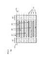
- FIG. 1 illustrates a multi-level VNCAP 100 with orthogonal adjacent metal level fingers, according to an exemplary embodiment.
- fingers 101 having a separation distance configured for a nominal voltage level are connected to nets by vias 103 and high voltage fingers 105 having a larger separation distance for a greater than nominal voltage level are connected to nets by large vias 107 .
- the large separation distance is a multiple (e.g., 3 times or 72 nm) of the smaller separation distance (e.g., 24 nm).
- fingers 201 of adjacent layers extend parallel to each other and are connected to nets through vias 203 .
- FIG. 3 illustrates a single layer 300 of a VNCAP for a nominal operating voltage, according to an exemplary embodiment.
- the layer 300 includes a first comb formed by a mandrel region having a vertical segment 301 (e.g., strap) and routes 303 (e.g., fingers) and a second comb formed by a non-mandrel region having a vertical segment 305 (e.g., strap) and routes 307 (e.g., fingers).
- each of the routes 303 and 307 is placed on one of equally spaced vertical positions 309 and has a width 311 (e.g., 24 nm) equal to a separation distance 313 between the routes 303 and 307 .
- routes 303 and 307 of the first and second combs, respectively, are interdigitated and connected to other layers to create 3D negative and positive plates.
- FIGS. 4 through 6 illustrate a method for providing a single layer of a VNCAP for a nominal operating voltage, according to exemplary embodiments.
- a mandrel region is provided on a substrate 400 to form horizontal portions 401 , vertical portion 403 , and a portion 405 to surround an intended vertical segment region 407 .
- a non-mandrel region having horizontal portions 501 and vertical segment 503 is provided using a traditional SADP process.
- spacers having a width equal to separation distance 313 are placed on sides of horizontal portions 401 , vertical portion 403 , and a portion 405 of the mandrel region, and the resulting non-mandrel region is provided as outside the separation distance 313 from the mandrel region.
- the SADP process results in the vertical segment 503 being provided in the intended vertical segment region 407 .
- a block mask 601 is provided over the portion 405 of the mandrel region to form the single layer 300 .
- the block mask 601 is separated from (e.g., not overlapping) the horizontal portions 401 and vertical portion 403 of the mandrel region and the horizontal portions 501 and vertical segment 503 of the non-mandrel region.
- the block mask 601 prevents an etching of portions of the substrate covered by the block mask 601 , thereby preventing metal to be formed in mandrel (and non-mandrel) regions covered by the block mask 601 .
- spacers abutting the mandrel region (e.g., 401 and 403 ) and the block mask 601 prevent etching of covered portions, resulting in mandrel recesses being formed in the mandrel region (e.g., 401 and, 403 ) and non-mandrel recesses being formed in the non-mandrel region (e.g., 501 and 503 ).
- a conductive material e.g., metal
- the single layer 300 is positioned on another layer or level having fingers 701 and 703 of the first and second nets, respectively.
- the fingers 701 and 703 are positioned to extend orthogonally to routes 303 and 307 .
- the fingers 701 and 703 are positioned to extend parallel to routes 303 and 307 .
- FIG. 8 a cross-sectional view illustrates a VNCAP 800 having the routes 303 and 307 extending orthogonally to a finger 703 and to a finger 801 of another layer or level.
- routes 303 and finger 801 are (part of) the same net (e.g., first). Additional levels or layers may be added, for instance, a layer above the finger 801 and a layer below the finger 703 running parallel to the routes 303 and 307 .
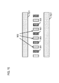
- FIG. 9 illustrates a single layer 900 for a VNCAP operating at a voltage greater than nominal, according to an exemplary embodiment.
- the layer 900 includes a first net having routes 901 and 903 , a second net having routes 905 and 907 , and routes 909 separated, for instance, by an electrical insulator from the first and second nets.
- the routes 901 , 905 , and 909 are each positioned on one of equally spaced vertical positions 911 , have a width 913 , and are separated from each other by a distance 915 equal to the width 913 .
- the routes 909 are floating or island nodes and positioned between the first and second nets having routes 901 and 905 interdigitated, resulting in an improved capacitive density.
- FIGS. 10 through 12 illustrate a method for providing a single layer of a VNCAP operating at a voltage greater than nominal, according to exemplary embodiments.
- a mandrel region is provided having horizontal portions 1001 and vertical portions 1003 and 1005 .
- a non-mandrel region having non-mandrel portions 1101 extending horizontally on substrate 1000 is provided as a result of using a traditional SADP process, for instance, as described above.
- Adverting to FIG. 12 a block mask having alternating first and second vertical segments 1201 and 1203 , respectively, is provided on the horizontal portions 1001 to provide the single layer 900 .
- the segments 1201 and 1203 are abutting (e.g., adjacent but not overlapping) the vertical portions 1003 and 1005 of the mandrel region. As such, the segments 1201 and 1203 prevent an etching of portions of the substrate 1000 covered by the segments 1201 and 1203 , thereby preventing metal to be formed in mandrel regions (e.g., 1001 ) covered by the segments 1201 and 1203 .
- the single layer 900 is provided on another layer having fingers 1301 (e.g., routes 901 , 905 , and 909 ). As shown, the fingers 1301 are positioned to extend orthogonally to routes 901 , 905 , and 909 . Alternatively, the fingers 1301 are positioned to extend parallel to routes 901 , 905 , and 909 .
- a cross-sectional view illustrates a VNCAP 1400 having the routes 901 , 905 , and 909 extending orthogonally to a finger 1301 and to a finger 1401 of another layer.
- the finger 1301 and the routes 901 are of the first net and finger 1401 and routes 905 are of the second net. Additional levels or layers may be added, for instance, a layer above the finger 1401 and a layer below the finger 1301 running parallel to the routes 901 , 905 , and 909 . Additionally or alternatively, the layer 900 of FIG. 9 , can be between two floating fingers 1501 (e.g., routes 909 ) of adjacent layers as shown in FIG. 15 .
- FIG. 16 illustrates a single layer 1600 for another VNCAP operating at a voltage greater than nominal, according to an exemplary embodiment.
- the layer 1600 includes a first net having routes 1601 and 1603 and a second net having routes 1605 and 1607 .
- the routes 1601 and 1605 are each positioned on one of equally spaced vertical positions 1609 have a width 1611 and are separated from each other by a distance 1613 equal to a multiple (e.g., 3 ) of the width 1611 .
- FIG. 17 illustrates a method for providing another single layer of a VNCAP operating at a voltage greater than nominal, according to exemplary embodiments.
- Adverting to FIG. 17 the resulting mandrel and non-mandrel regions of FIG. 11 are provided on a substrate 1700 as described above to provide the layer 1600 of FIG. 16 .
- the block mask includes horizontal portions 1705 extending an entire distance 1707 separating the vertical portions 1003 and 1005 .
- the portions 1701 , 1703 , and 1705 prevent an etching of portions of the substrate 1700 covered by the portions 1701 , 1703 , and 1705 , thereby preventing metal to be formed in mandrel regions (e.g., 1001 ) and non-mandrel regions (e.g., 1101 ) covered by the portions 1701 , 1703 , and 1705 .
- mandrel regions e.g., 1001
- non-mandrel regions e.g., 1101
- the single layer 1600 is provided on another layer having fingers 1801 (e.g., routes 1601 and 1605 ). As shown, the fingers 1801 are positioned to extend orthogonally to routes 1601 and 1605 . Alternatively, the fingers 1801 are positioned to extend parallel to routes 1601 and 1605 .
- FIG. 19 a cross-sectional view illustrates a VNCAP 1900 having the routes 1601 and 1605 extending orthogonally to a finger 1801 and to a finger 1901 of another layer. As shown, the finger 1801 and the routes 1601 are of the first net and finger 1901 and routes 1605 are of the second net. Additional levels or layers may be added, for instance, a layer above the finger 1901 and a layer below the finger 1801 running parallel to the routes 1601 and 1605 .
- routes 909 as illustrated in FIG. 9 , which are electronically isolated (e.g., separated, floating, etc.) from nets of the BEoL VNCAP (e.g., routes 901 and 905 ) results in an improvement of 50% in capacitance density.
- the embodiments of the present disclosure can achieve several technical effects, including an integration of capacitive components into ICs, resulting in ICs having a higher capacitive density and a lower cost.
- the present disclosure enjoys industrial applicability in any of various types of highly integrated semiconductor devices, particularly ICs having BEoL VNCAPs and utilizing SADP technology for a 10 nm technology node and beyond.
Landscapes
- Engineering & Computer Science (AREA)
- Computer Hardware Design (AREA)
- Physics & Mathematics (AREA)
- Theoretical Computer Science (AREA)
- Computer Networks & Wireless Communication (AREA)
- Evolutionary Computation (AREA)
- Geometry (AREA)
- General Engineering & Computer Science (AREA)
- General Physics & Mathematics (AREA)
- Semiconductor Integrated Circuits (AREA)
Abstract
Description
Claims (20)
Priority Applications (1)
| Application Number | Priority Date | Filing Date | Title |
|---|---|---|---|
| US13/948,249 US8856715B1 (en) | 2013-07-23 | 2013-07-23 | Capacitor designs for integrated circuits utilizing self-aligned double patterning (SADP) |
Applications Claiming Priority (1)
| Application Number | Priority Date | Filing Date | Title |
|---|---|---|---|
| US13/948,249 US8856715B1 (en) | 2013-07-23 | 2013-07-23 | Capacitor designs for integrated circuits utilizing self-aligned double patterning (SADP) |
Publications (1)
| Publication Number | Publication Date |
|---|---|
| US8856715B1 true US8856715B1 (en) | 2014-10-07 |
Family
ID=51627128
Family Applications (1)
| Application Number | Title | Priority Date | Filing Date |
|---|---|---|---|
| US13/948,249 Expired - Fee Related US8856715B1 (en) | 2013-07-23 | 2013-07-23 | Capacitor designs for integrated circuits utilizing self-aligned double patterning (SADP) |
Country Status (1)
| Country | Link |
|---|---|
| US (1) | US8856715B1 (en) |
Cited By (4)
| Publication number | Priority date | Publication date | Assignee | Title |
|---|---|---|---|---|
| CN108630651A (en) * | 2017-03-20 | 2018-10-09 | 格芯公司 | On-chip capacitance device with chinampa |
| US10109706B1 (en) | 2017-07-07 | 2018-10-23 | Globalfoundries Inc. | Method of forming high performance vertical natural capacitor (VNCAP) |
| US10211089B2 (en) | 2016-09-22 | 2019-02-19 | Samsung Electronics Co., Ltd. | Semiconductor device and method of fabricating the same |
| US20220344257A1 (en) * | 2021-04-26 | 2022-10-27 | Nxp B.V. | Fringe capacitor arranged based on metal layers with a selected orientation of a preferred direction |
Citations (12)
| Publication number | Priority date | Publication date | Assignee | Title |
|---|---|---|---|---|
| US5245750A (en) * | 1992-02-28 | 1993-09-21 | Hughes Aircraft Company | Method of connecting a spaced ic chip to a conductor and the article thereby obtained |
| US6166333A (en) * | 1998-01-14 | 2000-12-26 | Packard Hughes Interconnect Company | Bumps with plural under-bump dielectric layers |
| US6880134B2 (en) * | 2003-04-09 | 2005-04-12 | Freescale Semiconductor, Inc. | Method for improving capacitor noise and mismatch constraints in a semiconductor device |
| US20060088772A1 (en) * | 2001-10-02 | 2006-04-27 | Guobiao Zhang | Pattern-Distributed Mask |
| US7305643B2 (en) * | 2005-05-12 | 2007-12-04 | Freescale Semiconductor, Inc. | Method of tiling analog circuits that include resistors and capacitors |
| US7689961B2 (en) * | 2005-08-10 | 2010-03-30 | International Business Machines Corporation | Increased power line noise immunity in IC using capacitor structure in fill area |
| US20110061031A1 (en) * | 2007-02-15 | 2011-03-10 | United Microelectronics Corp. | Method for producing layout of semiconductor integrated circuit with radio frequency devices |
| US8255858B2 (en) * | 2008-11-26 | 2012-08-28 | Broadcom Corporation | Method for adjusting capacitance of capacitors without affecting die area |
| US20120254820A1 (en) * | 2011-03-28 | 2012-10-04 | International Business Machines Corporation | Method, a program storage device and a computer system for modeling the total contact resistance of a semiconductor device having a multi-finger gate structure |
| US8418120B2 (en) * | 2011-07-21 | 2013-04-09 | International Business Machines Corporation | Solutions for netlist reduction for multi-finger devices |
| US8435884B2 (en) * | 2010-09-07 | 2013-05-07 | Globalfoundries Inc. | Method for forming an interconnect structure |
| US8601430B1 (en) * | 2012-08-28 | 2013-12-03 | Freescale Semiconductor, Inc. | Device matching tool and methods thereof |
-
2013
- 2013-07-23 US US13/948,249 patent/US8856715B1/en not_active Expired - Fee Related
Patent Citations (15)
| Publication number | Priority date | Publication date | Assignee | Title |
|---|---|---|---|---|
| US5245750A (en) * | 1992-02-28 | 1993-09-21 | Hughes Aircraft Company | Method of connecting a spaced ic chip to a conductor and the article thereby obtained |
| US6166333A (en) * | 1998-01-14 | 2000-12-26 | Packard Hughes Interconnect Company | Bumps with plural under-bump dielectric layers |
| US20060088772A1 (en) * | 2001-10-02 | 2006-04-27 | Guobiao Zhang | Pattern-Distributed Mask |
| US6880134B2 (en) * | 2003-04-09 | 2005-04-12 | Freescale Semiconductor, Inc. | Method for improving capacitor noise and mismatch constraints in a semiconductor device |
| US7305643B2 (en) * | 2005-05-12 | 2007-12-04 | Freescale Semiconductor, Inc. | Method of tiling analog circuits that include resistors and capacitors |
| US7689961B2 (en) * | 2005-08-10 | 2010-03-30 | International Business Machines Corporation | Increased power line noise immunity in IC using capacitor structure in fill area |
| US20110061031A1 (en) * | 2007-02-15 | 2011-03-10 | United Microelectronics Corp. | Method for producing layout of semiconductor integrated circuit with radio frequency devices |
| US8255858B2 (en) * | 2008-11-26 | 2012-08-28 | Broadcom Corporation | Method for adjusting capacitance of capacitors without affecting die area |
| US8627259B2 (en) * | 2008-11-26 | 2014-01-07 | Broadcom Corporation | Capacitance modification without affecting die area |
| US8627258B2 (en) * | 2008-11-26 | 2014-01-07 | Broadcom Corporation | Adjusting capacitance of capacitors without affecting die area |
| US8435884B2 (en) * | 2010-09-07 | 2013-05-07 | Globalfoundries Inc. | Method for forming an interconnect structure |
| US20120254820A1 (en) * | 2011-03-28 | 2012-10-04 | International Business Machines Corporation | Method, a program storage device and a computer system for modeling the total contact resistance of a semiconductor device having a multi-finger gate structure |
| US8458642B2 (en) * | 2011-03-28 | 2013-06-04 | International Business Machines Corporation | Method, a program storage device and a computer system for modeling the total contact resistance of a semiconductor device having a multi-finger gate structure |
| US8418120B2 (en) * | 2011-07-21 | 2013-04-09 | International Business Machines Corporation | Solutions for netlist reduction for multi-finger devices |
| US8601430B1 (en) * | 2012-08-28 | 2013-12-03 | Freescale Semiconductor, Inc. | Device matching tool and methods thereof |
Cited By (7)
| Publication number | Priority date | Publication date | Assignee | Title |
|---|---|---|---|---|
| US10211089B2 (en) | 2016-09-22 | 2019-02-19 | Samsung Electronics Co., Ltd. | Semiconductor device and method of fabricating the same |
| CN108630651A (en) * | 2017-03-20 | 2018-10-09 | 格芯公司 | On-chip capacitance device with chinampa |
| US10147783B2 (en) * | 2017-03-20 | 2018-12-04 | Globalfoundries Inc. | On-chip capacitors with floating islands |
| CN108630651B (en) * | 2017-03-20 | 2021-12-17 | 格芯(美国)集成电路科技有限公司 | On-chip capacitor with floating island |
| US10109706B1 (en) | 2017-07-07 | 2018-10-23 | Globalfoundries Inc. | Method of forming high performance vertical natural capacitor (VNCAP) |
| US20220344257A1 (en) * | 2021-04-26 | 2022-10-27 | Nxp B.V. | Fringe capacitor arranged based on metal layers with a selected orientation of a preferred direction |
| US11532546B2 (en) * | 2021-04-26 | 2022-12-20 | Nxp B.V. | Fringe capacitor arranged based on metal layers with a selected orientation of a preferred direction |
Similar Documents
| Publication | Publication Date | Title |
|---|---|---|
| US11817385B2 (en) | Integrated circuit with guard ring | |
| US8921225B2 (en) | Method for off-grid routing structures utilizing self aligned double patterning (SADP) technology | |
| US8558350B2 (en) | Metal-oxide-metal capacitor structure | |
| US8856715B1 (en) | Capacitor designs for integrated circuits utilizing self-aligned double patterning (SADP) | |
| CN106816427B (en) | The capacitor arrangement of scalable fixation area occupied | |
| US20140246791A1 (en) | 14 lpm contact power rail | |
| US9524964B2 (en) | Capacitor structure in an integrated circuit | |
| TWI487123B (en) | Metal-oxide-metal capacitor | |
| US11817452B2 (en) | Method for forming decoupling capacitors between the interposing conductors and the multiple gates | |
| US8493708B2 (en) | Capacitor structure | |
| JP2012509596A (en) | Integrated capacitor with alternating stacked segments | |
| US8719757B2 (en) | Method to enhance double patterning routing efficiency | |
| CN107785363B (en) | MOM (metal oxide semiconductor) capacitor layout, structure unit and modeling method thereof | |
| US20150097249A1 (en) | Cross coupling gate using mulitple patterning | |
| TWI707480B (en) | Capacitor structure | |
| CN103700645A (en) | MOM (metal-oxide-metal) capacitor and manufacturing method thereof | |
| US9406605B2 (en) | Integrated circuit with guard ring | |
| KR101487591B1 (en) | Mom capacitor | |
| JP6264170B2 (en) | Semiconductor device | |
| US8357584B2 (en) | Metal capacitor design for improved reliability and good electrical connection | |
| CN105095533B (en) | A method of establishing metal-insulator-metal capacitor model | |
| US10096543B2 (en) | Semiconductor capacitor structure for high voltage sustain | |
| CN108346676B (en) | Semiconductor device with a plurality of transistors | |
| CN103000624B (en) | Capacitor structure applicable to integrated circuit | |
| JP2010135530A (en) | Semiconductor device |
Legal Events
| Date | Code | Title | Description |
|---|---|---|---|
| AS | Assignment |
Owner name: GLOBALFOUNDRIES INC., CAYMAN ISLANDS Free format text: ASSIGNMENT OF ASSIGNORS INTEREST;ASSIGNORS:STEPHENS, JASON E.;CHAUHAN, VIKRANT;CLEVENGER, LAWRENCE;AND OTHERS;SIGNING DATES FROM 20130711 TO 20130715;REEL/FRAME:033384/0229 |
|
| AS | Assignment |
Owner name: GLOBALFOUNDRIES INC., CAYMAN ISLANDS Free format text: ASSIGNMENT OF ASSIGNORS INTEREST;ASSIGNORS:STEPHENS, JASON E.;CHAUHAN, VIKRANT;CLEVENGER, LAWRENCE;AND OTHERS;SIGNING DATES FROM 20130712 TO 20141229;REEL/FRAME:034727/0960 Owner name: INTERNATIONAL BUSINESS MACHINES CORPORATIONS, NEW Free format text: ASSIGNMENT OF ASSIGNORS INTEREST;ASSIGNORS:STEPHENS, JASON E.;CHAUHAN, VIKRANT;CLEVENGER, LAWRENCE;AND OTHERS;SIGNING DATES FROM 20130712 TO 20141229;REEL/FRAME:034727/0960 |
|
| AS | Assignment |
Owner name: GLOBALFOUNDRIES INC., CAYMAN ISLANDS Free format text: CORRECTIVE ASSIGNMENT TO CORRECT THE NATURE OF CONVEYANCE TO ADD A SECOND ASSIGNEE NAME PREVIOUSLY RECORDED AT REEL: 033384 FRAME: 0229. ASSIGNOR(S) HEREBY CONFIRMS THE ASSIGNMENT;ASSIGNORS:STEPHENS, JASON E.;CHAUHAN, VIKRANT;CLEVENGER, LAWRENCE;AND OTHERS;SIGNING DATES FROM 20130711 TO 20141229;REEL/FRAME:035453/0617 Owner name: INTERNATIONAL BUSINESS MACHINES CORPORATIONS, NEW Free format text: CORRECTIVE ASSIGNMENT TO CORRECT THE NATURE OF CONVEYANCE TO ADD A SECOND ASSIGNEE NAME PREVIOUSLY RECORDED AT REEL: 033384 FRAME: 0229. ASSIGNOR(S) HEREBY CONFIRMS THE ASSIGNMENT;ASSIGNORS:STEPHENS, JASON E.;CHAUHAN, VIKRANT;CLEVENGER, LAWRENCE;AND OTHERS;SIGNING DATES FROM 20130711 TO 20141229;REEL/FRAME:035453/0617 |
|
| FEPP | Fee payment procedure |
Free format text: MAINTENANCE FEE REMINDER MAILED (ORIGINAL EVENT CODE: REM.) |
|
| LAPS | Lapse for failure to pay maintenance fees |
Free format text: PATENT EXPIRED FOR FAILURE TO PAY MAINTENANCE FEES (ORIGINAL EVENT CODE: EXP.); ENTITY STATUS OF PATENT OWNER: LARGE ENTITY |
|
| STCH | Information on status: patent discontinuation |
Free format text: PATENT EXPIRED DUE TO NONPAYMENT OF MAINTENANCE FEES UNDER 37 CFR 1.362 |
|
| AS | Assignment |
Owner name: WILMINGTON TRUST, NATIONAL ASSOCIATION, DELAWARE Free format text: SECURITY AGREEMENT;ASSIGNOR:GLOBALFOUNDRIES INC.;REEL/FRAME:049490/0001 Effective date: 20181127 |
|
| FP | Lapsed due to failure to pay maintenance fee |
Effective date: 20181007 |
|
| AS | Assignment |
Owner name: GLOBALFOUNDRIES INC., CAYMAN ISLANDS Free format text: RELEASE BY SECURED PARTY;ASSIGNOR:WILMINGTON TRUST, NATIONAL ASSOCIATION;REEL/FRAME:054636/0001 Effective date: 20201117 |
|
| AS | Assignment |
Owner name: GLOBALFOUNDRIES U.S. INC., NEW YORK Free format text: RELEASE BY SECURED PARTY;ASSIGNOR:WILMINGTON TRUST, NATIONAL ASSOCIATION;REEL/FRAME:056987/0001 Effective date: 20201117 |