US8856577B2 - Semiconductor device having multiplexer - Google Patents
Semiconductor device having multiplexer Download PDFInfo
- Publication number
- US8856577B2 US8856577B2 US13/290,541 US201113290541A US8856577B2 US 8856577 B2 US8856577 B2 US 8856577B2 US 201113290541 A US201113290541 A US 201113290541A US 8856577 B2 US8856577 B2 US 8856577B2
- Authority
- US
- United States
- Prior art keywords
- power
- circuit
- power supply
- internal
- voltage
- Prior art date
- Legal status (The legal status is an assumption and is not a legal conclusion. Google has not performed a legal analysis and makes no representation as to the accuracy of the status listed.)
- Active, expires
Links
Images


Classifications
-
- H—ELECTRICITY
- H03—ELECTRONIC CIRCUITRY
- H03K—PULSE TECHNIQUE
- H03K3/00—Circuits for generating electric pulses; Monostable, bistable or multistable circuits
- H03K3/02—Generators characterised by the type of circuit or by the means used for producing pulses
- H03K3/353—Generators characterised by the type of circuit or by the means used for producing pulses by the use, as active elements, of field-effect transistors with internal or external positive feedback
- H03K3/356—Bistable circuits
- H03K3/356104—Bistable circuits using complementary field-effect transistors
- H03K3/356113—Bistable circuits using complementary field-effect transistors using additional transistors in the input circuit
Definitions
- the present invention relates to a semiconductor device, and more particularly to a semiconductor device that includes a multiplexer which outputs internal data signals in synchronization with a plurality of internal clock signals having different phases.
- a clocked gate circuit is used as the synchronizing circuit.
- internal data signals have the same amplitude as that of an internal power supply voltage which is lower than an external power supply voltage.
- a level shift circuit is therefore inserted into the signal paths of the internal data signals. Since the level shift circuit is inserted in a position immediately before the clocked gate circuit, the clocked gate circuit operates on the external power supply voltage as its power source.
- DDR Double Data Rate
- data is output in synchronization with both edges (rising edge and falling edge) of a clock signal.
- Such type of semiconductor devices need a multiplexer having clocked gate circuits connected in parallel, and a clock dividing circuit for generating complementary internal clock signals. With such a configuration, there has been a possibility of interaction among noises and a drop in signal quality if the multiplexer and the clock dividing circuit are operated with the same internal power supply voltage.
- a semiconductor device that includes: a DLL circuit that generates a first internal clock signal based on an external clock signal; a clock dividing circuit that generates second and third internal clock signals having different phases based on the first internal clock signal; a multiplexer that outputs second and third internal data signals based on a first internal data signal in synchronization with one of the second and third clock signals; a plurality of power supply circuits each generating an internal power supply voltage, the internal power supply voltage supplied to the clock dividing circuit and the internal power supply voltage supplied to the multiplexer being generated by respective different power supply circuits and being separated from each other in the semiconductor device.
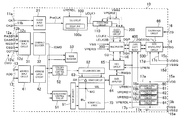
- FIG. 1 is a block diagram showing the configuration of a semiconductor device 10 according to an embodiment of the present invention
- FIG. 2 is a schematic sectional view for explaining the separation on a well level
- FIG. 3 is a circuit diagram of a clock dividing circuit 200 shown in FIG. 1 ;
- FIG. 4 is a detailed circuit diagram of the clock dividing circuit 200 shown in FIG. 3 ;
- FIG. 5 is a waveform chart for explaining the operation of the clock dividing circuit 200 shown in FIG. 3 ;
- FIG. 6 is a circuit diagram of a multiplexer 300 shown in FIG. 1 ;
- FIG. 7 is a block diagram of a level shift block 400 and a data input/output circuit 500 shown in FIG. 1 ;
- FIG. 8 is a block diagram showing the configuration of a level shift circuit unit 410 shown in FIG. 7 ;
- FIG. 9A is a circuit diagram of a level shift circuit LV 1 shown in FIG. 8 ;
- FIG. 9B is a circuit diagram of a level shift circuit LV 2 shown in FIG. 8 ;
- FIG. 10 is a waveform chart showing the operation of the level shift circuit unit 410 ;
- FIG. 11 is a simulation result showing the relationship between a difference ⁇ tPD in delay time and the external power supply potential VDD when using the level shift circuit unit 410 shown in FIG. 8 ;
- FIG. 12 is a simulation result showing the relationship between the time difference ⁇ tPD and the external power supply potential VDD according to a comparative example
- FIG. 13 is a circuit diagram of an impedance control circuit 510 shown in FIG. 7 ;
- FIG. 14 is a circuit diagram of an output buffer 501 shown in FIG. 7 ;
- FIG. 15 is a circuit diagram of the level shift circuit LV 3 according to a modification.
- FIG. 16 is a circuit diagram of the level shift circuit LV 3 according to another modification.
- a semiconductor device 10 is a DDR (Double Data Rate) SDRAM (Synchronous DRAM).
- the semiconductor device 10 has external terminals including clock terminals 11 a and 11 b , command terminals 12 a to 12 e , address terminals 13 , a data input/output terminal (data output terminal) 14 , power supply terminals 15 a to 15 e , and a calibration terminal 16 .
- the semiconductor device 10 also has other terminals such as a data strobe terminal and a reset terminal, which are omitted from the diagram.
- each of the terminals described above as well as circuit blocks constituting the DDR SDRAM are formed on a single semiconductor chip as the semiconductor device 10 , as surrounded by a dotted line in FIG. 1 . Further, each of the terminals may be also called “a pad” formed on the chip.
- the clock terminals 11 a and 11 b are supplied with external clock signals CK and CKB, respectively.
- the supplied external clock signals CK and CKB are supplied to a clock input circuit 21 .
- a signal having a signal name with a trailing “B” is either the inverted signal of a corresponding signal or a low-active signal.
- the external clock signals CK and CKB are thus mutually complementary signals.
- the clock input circuit 21 generates a single-phase internal clock signal PreCLK based on the external clock signals CK and CKB, and supplies the internal clock signal PreCLK to a DLL circuit 100 .
- the DLL circuit 100 generates a phase-controlled internal clock signal LCLK 1 based on the internal clock signal PreCLK, and supplies the internal clock signal LCLK 1 to a clock dividing circuit 200 through a clock tree circuit 110 .
- the clock dividing circuit 200 generates complementary internal clock signals LCLK 2 and LCLK 2 B from the single-phase internal clock signal LCLK 1 , and supplies the complementary internal clock signals LCLK 2 and LCLK 2 B to a multiplexer 300 .
- the command terminal 12 a to 12 e are supplied with a row address strobe signal RASB, a column address strobe signal CASB, a write enable signal WEB, a chip select signal CSB, and an on-die termination signal ODT, respectively.
- Such command signals CMD are supplied to a command decoder 32 through a command input circuit 31 .
- the command decoder 32 generates various internal commands ICMD by holding, decoding, or counting the command signals.
- the internal commands ICMD are supplied to a row-system control circuit 51 , a column-system control circuit 52 , and a mode register 53 .
- the address terminals 13 are supplied with address signals ADD.
- the address signals ADD input to the address terminals 13 are supplied to an address latch circuit 42 through an address input circuit 41 to be latched in the address latch circuit 42 .
- row addresses are supplied to the row-system control circuit 51 .
- Column addresses are supplied to the column system control circuit 52 .
- the address signals ADD are supplied to the mode register 53 , whereby contents of the mode register 53 are updated.
- Output signals of the row-system control circuit 51 are supplied to a row decoder 61 .
- the row decoder 61 selects any of word lines WL included in a memory cell array 70 .
- the memory cell array 70 includes a plurality of word lines WL and a plurality of bit lines BL which intersect each other.
- Memory cells MC are arranged at the intersections ( FIG. 1 shows only one of the word lines WL, one of the bit lines BL, and one of the memory cells MC).
- the bit lines BL are connected to corresponding sense amplifiers SA in a sense circuit 63 .
- the output signals of the column-system control circuit 52 are supplied to a column decoder 62 .
- the column decoder 62 selects any of the sense amplifiers SA included in the sense circuit 63 .
- the sense amplifiers SA selected by the column decoder 62 are connected to a data amplifier 64 .
- the data amplifier 64 In a read operation, the data amplifier 64 further amplifies read data that is amplified by the sense amplifiers SA, and supplies the read data to a FIFO circuit 65 through a read/write bus RWBS.
- the data amplifier 64 amplifies write data that is supplied from the FIFO circuit 65 through the read/write bus RWBS, and supplies the write data to sense amplifiers SA.
- the FIFO circuit 65 is connected to the multiplexer 300 .
- the FIFO circuit 65 constitutes a data transfer circuit for transferring data between the memory cell array 70 and the multiplexer 300 .
- the data input/output terminal 14 is an external terminal for outputting read data DQ to outside and receiving write data DQ from outside.
- the data input/output terminal 14 is connected to a data input/output circuit 500 .
- the data input/output circuit 500 is connected to the multiplexer 300 through a level shift block 400 .
- the data input/output circuit 500 drives the data input/output terminal 14 based on read data DQ that is supplied from the multiplexer 300 through the level shift block 400 . While FIG. 1 shows only one data input/output terminal 14 , the number of data input/output terminals 14 need not necessarily be one. There may be provided a plurality of data input/output terminals 14 .
- the data input/output circuit 500 is also connected to a calibration circuit 66 .
- the calibration circuit 66 is connected to the calibration terminal 16 , and functions to adjust the impedance of an output buffer included in the data input/output circuit 500 .
- the calibration circuit 66 performs a calibration operation to generate an impedance code ZQCODE, and supplies the impedance code ZQCODE to the data input/output circuit 500 .
- the data input/output circuit 500 changes the impedance of the output buffer based on the impedance code ZQCODE.
- the impedance adjusting operation by the calibration circuit 66 is intended to prevent the impedance of the output buffer from deviating from a set value due to temperature changes or voltage variations.
- the set value of the impedance itself can be changed by a set value of the mode register 53 .
- the power supply terminals 15 a and 15 b are supplied with an external power supply potential VDD and a ground potential VSS, respectively.
- a voltage between the external power supply potential VDD and the ground potential VSS may be referred to simply as “external voltage VDD.”
- the external voltage VDD is supplied to an internal voltage generating circuit 80 .
- the internal voltage generating circuit 80 includes a plurality of power supply circuits 81 to 84 , which generate respective internal power supply potentials VPERI, VPERI 2 , VPERI 3 , and VPERDL lower than the external power supply potential VDD.
- the internal power supply potentials VPERI, VPERI 2 , VPERI 3 , and VPERDL have the same level.
- a voltage between the internal power supply potential VPERI and the ground potential VSS may be referred to simply as “internal voltage VPERI.” The same applies to VPERI 2 , VPERI 3 , and VPERDL.
- the power supply terminals 15 c and 15 d are to be supplied with an external power supply potential VDDQ and a ground potential VSSQ, respectively.
- a voltage between the external power supply potential VDDQ and the ground potential VSSQ may be referred to simply as “external voltage VDDQ.”
- the external power supply potential VDDQ has the same level as that of the external power supply potential VDD.
- the ground potential VSSQ has the same level as that of the ground potential VSS.
- the power supply terminal 15 a and 15 c are separate terminals on the chip.
- a VDD line (high-potential power supply line) 17 a that is connected to the power supply terminal 15 a and a VDDQ line (high-potential power supply line) 17 c that is connected to the power supply terminal 15 c are also separate from each other, not being connected to each other in the chip.
- VSS line (low-potential power supply line) 17 b that is connected to the power supply terminal 15 b and a VSSQ line (low-potential power supply line) 17 d that is connected to the power supply terminal 15 d are separated from each other, not being connected to each other in the chip.
- Such separation of the power supply lines is intended to prevent power supply noise occurring due to the operation of the data input/output circuit 500 from propagating to other circuits.
- the VDDQ line 17 c and the VSSQ line 17 d are designed to be lower than the VDD line 17 a and the VSS line 17 b in impedance.
- the lower impedance can be obtained by making the numbers of power supply terminals 15 c and 15 d greater than those of power supply terminals 15 a and 15 b.
- the present embodiment also provides a power supply terminal 15 e supplied with a ground potential VSS 2 .
- a VSS 2 line 17 e connected to the power supply terminal 15 e is separated from the VSS line 17 b and the VSSQ line 17 d , being connected to neither of the lines in the chip.
- the internal power supply potentials VPERI, VPERI 2 , VPERI 3 , and VPERDL are identical in level.
- a VPERI line 18 a for supplying the internal power supply potential VPERI, a VPERI 2 line 18 b for supplying the internal power supply potential VPERI 2 , a VPERI 3 line 18 c for supplying the internal power supply potential VPERI 3 , and a VPERDL line 18 d for supplying the internal power supply potential VPERDL are separated from each other, not being connected to each other in the chip. Again, such separation is intended to prevent an interaction among noises through the power supply lines.
- “power supply lines being separated” means not only that such line is not short-circuited, but also that transistors using these internal power supply potentials are formed in respective different wells and are thereby separated on a well level.
- n-wells 2 a and 2 b are formed in a p-type silicon substrate 1 .
- P-channel MOS transistors 3 a and 3 b are formed in the n-wells 2 a and 2 b , respectively.
- a source of the transistor 3 a is connected to a power supply line 5 a through a contact conductor 4 a .
- a source of the transistor 3 b is connected to a power supply line 5 b through a contact conductor 4 b .
- the power supply line 5 a is any one of the VPERI line 18 a , VPERI 2 line 18 b , VPERI 3 line 18 c , and VPERDL line 18 d .
- the power supply line 5 b is any one of the VPERI line 18 a , VPERI 2 line 18 b , VPERI 3 line 18 c , and VPERDL line 18 d other than the power supply line 5 a .
- the internal power supply potentials VPERI, VPERI 2 , VPERI 3 , and VPERDL hardly affect each other by such separation on the well level even if these lines have the same potential level.
- the power supply circuits 81 to 84 that generate the internal power supply potentials VPERI, VPERI 2 , VPERI 3 , and VPERDL, respectively, are independent of each other.
- the power supply circuits 81 to 84 are also separated even in the internal voltage generation circuit 80 .
- the VDD line 17 a and the VSS line 17 b are connected to the level shift block 400 .
- the VDDQ line 17 c and the VSSQ line 17 d are connected to the data input/output circuit 500 .
- Such connection means that the level shift block 400 operates on the voltage (external voltage VDD) between the external power supply potential VDD and the ground potential VSS, and the data input/output circuit 500 operates on the voltage (external voltage VDDQ) between the external power supply potential VDDQ and the ground potential VSSQ.
- the VPERI 2 line 18 b is connected to the clock tree circuit 110 and the clock dividing circuit 200 .
- the clock tree circuit 110 and the clock dividing circuit 200 thus operate on the internal power supply voltage VPERI 2 .
- the VPERI 3 line 18 c is connected to the multiplexer 300 .
- the multiplexer 300 thus operates on the internal power supply voltage VPERI 3 .
- the VPERDL line 18 d is connected to the DLL circuit 100 .
- a delay line 100 a included in the DLL circuit 100 operates on the internal power supply voltage VPERDL.
- Most of the other peripheral circuits are connected with the VPERI line 18 a .
- Most of the peripheral circuits thus operate on the internal power supply voltage VPERI.
- FIG. 1 shows the internal power supply voltage VPERI being supplied to the FIFO circuit 65 .
- the memory cell array 70 also uses an array voltage (VARAY), a high voltage (VPP) which exceeds the external voltage VDD, and even a negative voltage (VKK). Such voltages are not directly relevant to the gist of the present invention, and description thereof will thus be omitted.
- VARAY array voltage
- VPP high voltage
- VKK negative voltage
- the clock dividing circuit 200 includes a signal path PASS 1 that generates the internal clock signal LCLK 2 B from the internal clock signal LCLK 1 .
- the clock dividing circuit 200 also includes a signal path PASS 2 that generates the internal clock signal LCLK 2 from the internal clock signal LCLK 1 .
- the signal path PASS 1 is to generate the internal clock signal LCLK 2 B which is reverse to the internal clock signal LCLK 1 in phase.
- the signal path PASS 1 includes three inverters 211 , 212 , and 213 .
- the signal path PASS 2 generates the internal clock signal LCLK 2 which is in phase with the internal clock signal LCLK 1 .
- the signal path PASS 2 includes two inverters 221 and 222 . The number of stages of the logic circuits included in the signal path PASS 1 is greater than that of the logic circuits included in the signal path PASS 2 by one.
- the inverters 211 to 213 and 222 operate with a voltage between the internal power supply potential VPERI 2 and the ground potential VSS 2 as the power source.
- the inverter 221 operates with an output signal of the inverter 211 , or an inverted signal INB, as the power source.
- a phase of an output signal of the inverter 212 , or an internal signal INTT coincides with a phase of an output signal of the inverter 221 , or an internal signal INBB, even if the signal paths PASS 1 and PASS 2 have different numbers of logic stages.
- the circuit configuration and operation of the clock dividing circuit 200 used in the present embodiment will be described in more detail.
- the inverters each include a series circuit of P- and N-channel MOS transistors. Each individual inverter will be described in detail below.
- the inverter 211 includes a series circuit of transistors P 211 and N 211 . Sources of the transistors P 211 and N 211 are connected to the VPERI 2 line 18 b and the VSS 2 line 17 e , respectively.
- the internal clock signal LCLK 1 is supplied to gate electrodes of the transistors P 211 and N 211 in common.
- An inverted signal INB is output from a common drain of the transistors P 211 and N 211 .
- the inverter 212 includes a series circuit of transistors P 212 - 1 and N 212 - 1 .
- the inverted signal INB is supplied in common to gate electrodes of the transistors P 212 - 1 and N 212 - 1 .
- the internal signal INTT is output from a common drain of the transistors P 212 - 1 and N 212 - 1 .
- a transistor P 212 - 2 is connected between a source of the transistor P 212 - 1 and the VPERI 2 line 18 b .
- the ground potential VSS 2 is supplied to a gate electrode of the transistor P 212 - 2 , whereby the transistor P 212 - 2 is fixed to an ON state.
- a transistor N 212 - 2 is connected between a source of the transistor N 212 - 1 and the VSS 2 line 17 e .
- the internal power supply potential VPERI 2 is supplied to a gate electrode of the transistor N 212 - 2 , whereby the transistor N 212 - 2 is fixed to an ON state.
- the inverter 213 includes a series circuit of transistors P 213 and N 213 . Sources of the transistors P 213 and N 213 are connected to the VPERI 2 line 18 b and the VSS 2 line 17 e , respectively.
- the internal signal INTT is supplied to gate electrodes of the transistors P 213 and N 213 in common.
- the internal clock signal LCLK 2 B is output from a common drain of the transistors P 213 and N 213 .
- the inverter 213 is to secure a fan-out. The provision of the inverter 213 is not indispensable in the present invention.
- the inverter 221 includes a series circuit of transistors P 221 and N 221 . Both sources of the transistors P 221 and N 221 are connected to an output end (common drain) of the inverter 211 .
- the internal clock signal LCLK 1 is supplied to gate electrodes in common of the transistors P 221 and N 221 .
- the internal signal INBB is output from a common drain of the transistors P 221 and N 221 .
- the inverter 222 includes a series circuit of transistors P 222 and N 222 . Sources of the transistors P 222 and N 222 are connected to the VPERI 2 line 18 b and the VSS 2 line 17 e , respectively.
- the internal signal INBB is supplied to gate electrodes of the transistors P 222 and N 222 in common.
- the internal clock signal LCLK 2 is output from a common drain of the transistors P 222 and N 222 .
- the inverter 222 is to secure a fan-out. The provision of the inverter 222 is not indispensable in the present invention.
- the N-channel MOS transistors N 211 , N 212 - 1 , N 212 - 2 , and N 221 are designed to have the same channel width.
- the N-channel MOS transistors N 211 , N 212 - 1 , N 212 - 2 , and N 221 therefore have the same ON resistance.
- the P-channel MOS transistors P 211 , P 212 - 1 , P 212 - 2 , and P 221 are designed to have the same channel width.
- the P-channel MOS transistors P 211 , P 212 - 1 , P 212 - 2 , and P 221 therefore have the same ON resistance.
- the transistors N 211 , N 212 - 1 , N 212 - 2 , N 221 , P 211 , P 212 - 1 , P 212 - 2 , and P 221 have the same ON resistance.
- the inverters 211 and 221 that receive the internal clock signal LCLK 1 start to invert their outputs, the inverted signal INB and the internal signal INBB. Since the inverter 221 is powered by an output signal of the inverter 211 , or the inverted signal INB, the inverter 221 is not able to invert the internal signal INBB (i.e., change the internal signal INBB to a low level) until the internal signal INB changes from a high level to a low level. At time t 11 , the inverted signal INB changes from a high level to a low level. At time t 12 , the internal signal INBB then changes from a high level to a low level.
- Time t 12 corresponds to a timing for respondent logic circuits in the next stage to make an inversion after the inverted signal INB changes from a high level to a low level.
- the output signal of the inverter 212 or the internal signal INTT, therefore also changes at time t 12 . That is, the inverters 212 and 221 simultaneously make a change at time t 12 .
- an output signal of the inverter 213 , or the internal clock signal LCLK 2 B, and an output signal of the inverter 222 , or the internal clock signal LCLK 2 simultaneously make a change at time t 13 .
- the internal clock signals LCLK 2 and LCLK 2 B eventually make a change at the same time.
- the transistor N 211 included in the inverter 211 turns ON to change the inverted signal INB from a high level to a low level.
- This change has the following effects on the logic circuits in the next stage:
- the transistor P 212 - 1 turns ON and an output end, or common drain, is connected to the VPERI 2 line 18 b through the transistors P 212 - 2 and P 212 - 1 .
- the transistor N 221 turns ON and an output end, or common drain, is connected to the VSS 2 line 17 e through the transistors N 211 and N 221 . Consequently, the internal signal INTT and the internal signal INBB always change at the same time if the series resistance of the transistors P 212 - 2 and P 212 - 1 and series resistance of the transistors N 211 and N 221 are designed to be the same.
- the transistor P 211 included in the inverter 211 turns ON to change the inverted signal INB from a low level to a high level.
- This change has the following effects on the logic circuits in the next stage:
- the transistor N 212 - 1 turns ON and an output end, or common drain, is connected to the VSS 2 line 17 e through the transistors N 212 - 2 and N 212 - 1 .
- the transistor P 221 turns ON and an output end, or common drain, is connected to the VPERI 2 line 18 b through the transistors P 211 and P 221 . Consequently, the internal signal INTT and the internal signal INBB always change at the same time if series resistance of the transistors N 212 - 2 and N 212 - 1 and series resistance of the transistors P 211 and P 221 are designed to be the same.
- the clock dividing circuit 200 used in the present embodiment uses the signal on the signal path PASS 1 as the power source of the inverter 221 which is included in the other signal path PASS 2 .
- Such a configuration allows precise matching of the pair of internal clock signals LCLK 2 and LCLK 2 B in phase without adding a capacitor or resistor for adjustment. This eliminates the need to change masks repeatedly for the sake of modifying capacitance value or resistance value, thereby allowing a reduction in design cost.
- the multiplexer 300 includes clocked drivers 301 to 304 .
- the clocked drivers 301 and 303 output an internal data signal CD supplied from the FIFO circuit 65 in synchronization with a rising edge of the internal clock signal LCLK 2 .
- the clocked drivers 302 and 304 outputs an internal data signal CE supplied from the FIFO circuit 65 in synchronization with the rising edge of the internal clock signal LCLK 2 B.
- Output signals of the clocked drivers 301 and 302 are output as pull-up data DQP through an inverter 310 .
- Outputs of the clocked drivers 303 and 304 are output as pull-down data DQN through an inverter 320 .
- All the clocked drivers 301 to 304 and the inverters 310 and 320 which constitute the multiplexer 300 operate on the internal power supply voltage VPERI 3 . That is, the high-level power supply nodes are connected to the VPERI 3 line 18 c . The low-level power supply nodes are connected to the VSS line 17 b.
- the level shift block 400 includes level shift circuit units 410 and 420 .
- the level shift circuit unit 410 converts the amplitude of the pull-up data DQP from VPERI 3 to VDD.
- the level shift circuit unit 420 converts an amplitude of the pull-down data DQN from VPERI 3 to VDD.
- a level-converted pull-up data DQP 0 from the level shift circuit unit 410 is supplied to the data input/output circuit 500 as pull-up data DQP 1 through gate circuits 431 and 432 .
- the level-converted pull-down data DQN 0 from the level shift circuit unit 420 is supplied to the data input/output circuit 500 as pull-down data DQN 1 through gate circuits 441 and 442 .
- the ones subsequent to the level shift circuit units 410 and 420 operate on a voltage between the external power supply potential VDD and the ground potential VSS (external voltage VDD).
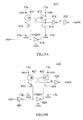
- the level shift circuit unit 410 includes two level shift circuits LV 1 and LV 2 , an inverter 401 which inverts the pull-up data DQP, and an inverter 402 which inverts an output signal of the level shift circuit LV 1 .
- the two level shift circuits LV 1 and LV 2 have the same circuit configuration.
- the pull-up data DQP without change of its logic is input to the level shift circuit LV 1 .
- An inverted signal of the pull-up data DQP, inverted by the inverter 401 is input to the level shift circuit LV 2 .
- the output signal of the level shift circuit LV 1 inverted by the inverter 402 and an output signal of the level shift circuit LV 2 are short-circuited and output as the pull-up data DQP 0 .
- the pull-up data DQP is simply input to the level shift circuit LV 1 .
- input circuits with any circuit configuration may be arranged in the stage prior to the level shift circuits LV 1 and LV 2 as long as complementary input signals are supplied to the level shift circuits LV 1 and LV 2 .
- the output signal of the level shift circuit LV 2 is simply short-circuited with the output signal of the inverter 402 .
- output circuits with any circuit configuration may be arranged in the stage subsequent to the level shift circuits LV 1 and LV 2 as long as the complementary output signals output from the level shift circuits LV 1 and LV 2 are converted into in-phase signals before short-circuited.
- the level shift circuit LV 1 includes P-channel MOS transistors 411 and 412 and N-channel MOS transistors 413 and 414 .
- the transistors 411 and 412 are connected to the VDD line 17 a at their sources and are cross-coupled with each other.
- the transistors 413 and 414 are connected to the VSS line 17 b at their sources and are connected in series to the transistors 411 and 412 , respectively.
- the pull-up data DQP is simply supplied to a gate electrode of the transistor 413 .
- the pull-up data DQP is supplied to a gate electrode of the transistor 414 through an inverter 415 .
- the level-shifted output signal is taken out from a node between the transistors 412 and 414 , and output as the pull-up data DQP 0 through inverters 416 and 402 .
- the level shift circuit LV 2 has exactly the same circuit configuration as the level shift circuit LV 1 . More specifically, the level shift circuit LV 2 includes P-channel MOS transistors 421 and 422 and N-channel MOS transistors 423 and 424 .
- the transistors 421 and 422 are connected to the VDD line 17 a at their sources and are cross-coupled with each other.
- the transistors 423 and 424 are connected to the VSS line 17 b at their sources and are connected in series to the transistors 421 and 422 , respectively.
- the pull-up data DQP is supplied to a gate electrode of the transistor 423 through the inverter 401 .
- the pull-up data DQP is supplied to a gate electrode of the transistor 424 through the inverters 401 and 425 .
- the level-shifted output signal is taken out from the node between the transistors 422 and 424 , and output as the pull-up data DQP 0 through an inverter 426 .
- the output signal of the level shift circuit LV 2 and the output signal of the level shift circuit LV 1 through the inverter 402 are short-circuited. This synthesizes the output signals of the level shift circuits LV 1 and LV 2 , so that the pull-up data DQP 0 has a composite waveform.
- the level shift circuit unit 410 includes the two level shift circuits LV 1 and LV 2 , the number of elements is twice that of an ordinary level shift circuit. Each element, however, need only have half the size in an ordinary level shift circuit because the two level shift circuits LV 1 and LV 2 operate in parallel. Despite twice the number of elements, the occupied area on the chip is almost the same as with an ordinary level shift circuit.
- signals A and B are internal signals of the level shift circuits LV 1 and LV 2 , respectively.
- the signal A represents an output level of the inverter 416 .
- the signal B represents a level of a node between the transistors 422 and 424 .
- both the signals A and B change from a low level to a high level at slightly different slew rates. Specifically, the signal A rises more sharply than the signal B.
- the signals A and B are passed through the inverters 402 and 426 , respectively, and then short-circuited.
- the two signals having different slew rates are thereby synthesized into a steeper waveform. Similar synthesis also takes place when the pull-up data DQP changes from a low level to a high level.
- the input pull-up data DQP and the output pull-up data DQP 0 therefore have almost the same duty cycles. Since the signals A and B having different slew rates are passed through the respective inverters 402 and 426 before short-circuited, no through current will flow if fan-out and other factors of the inverters 423 and 426 are appropriately designed.
- the difference ⁇ tPD represents a difference between a delay time at the rise and a delay time at the fall of the pull-up data DQP.
- the condition C 1 shown in FIG. 11 refers to a case where the ambient temperature is 110° C. and the transistor threshold is higher than a designed value due to process variations. That is, the transistor in condition C 1 operates slower speed compared with a typical speed.
- the condition C 2 refers to a case where the ambient temperature is 45° C. and the transistor threshold is higher than a designed value due to process variations.
- the condition C 3 refers to a case where the ambient temperature is 45° C. and the transistor threshold is as designed. That is, the transistor in condition C 3 operates at a typical speed.
- the condition C 4 refers to a case where the ambient temperature is 45° C. and the transistor threshold is lower than a designed value due to process variations.
- the transistor in condition C 4 operates faster speed compared with a typical speed.
- the condition C 5 refers to a case where the ambient temperature is ⁇ 5° C. and the transistor threshold is lower than a designed value due to process variations.
- the condition C 6 refers to a case where the ambient temperature is 45° C., the N-channel MOS transistors have a threshold higher than a designed value, and the P-channel MOS transistors have a threshold lower than a designed value due to process variations.
- the condition C 7 refers to a case where the ambient temperature is 45° C., the N-channel MOS transistors have a threshold lower than a designed value, and the P-channel MOS transistors have a threshold higher than a designed value due to process variations.
- the leftmost value is for a situation when the external power supply potential VDD is 1.2 V.
- the rightmost value is for a situation when the external power supply potential VDD is 2.0 V.
- the values therebetween are at potential pitches of 0.1 V.
- the use of the level shift circuit unit 410 according to the present embodiment brings the difference ⁇ tPD between the delay time at the rise and the delay time at the fall of the pull-up data DQP close to zero.
- the tendency is little affected by the level of the external power supply potential VDD, the temperature condition, or the process condition.
- the simulation result shown in FIG. 12 is for the case of using only one of the level shift circuits LV 1 and LV 2 . It should be noted that the transistor sizes are adjusted to approximately twice in order to provide the same measurement condition as in FIG. 11 . In other respects, the measurement condition is the same as in FIG. 11 . As shown in FIG. 12 , it can be seen that the time difference ⁇ tPD according to the comparative example has high VDD dependence. The tendency varies with the temperature condition and the process condition.
- the level shift circuit unit 420 can also provide the foregoing effect since the level shift circuit unit 420 has exactly the same circuit configuration as that of the level shift circuit unit 410 .
- the pull-up data DQP 0 output from the level shift circuit units 410 is input to the impedance control circuit 510 as pull-up data DQP 1 through the gate circuits 431 and 432 .
- the pull-down data DQN 0 output from the level shift circuit units 420 is input to the impedance control circuit 510 as pull-down data DQN 1 through the inverters 441 and 442 .
- the impedance control circuit 510 includes five OR circuits 521 to 525 (pull-up logic circuits) and five AND circuits 531 to 535 (pull-down logic circuits).
- the pull-up data DQP 1 from the level shift circuit unit 410 is supplied to the OR circuits 521 to 525 in common.
- Bits DRZQP 1 to DRZQP 5 of a pull-up impedance adjustment code DRZQP are also supplied to the OR circuits 521 to 525 , respectively.
- the pull-down data DQN 1 from the level shift circuit unit 420 is supplied to the AND circuits 531 to 535 in common.
- Bits DRZQN 1 to DRZQN 5 of a pull-down impedance adjustment code DRZQN are also supplied to the AND circuits 531 to 535 , respectively.
- the pull-up impedance adjustment code DRZQP and the pull-down impedance adjustment code DRZQN are signals that constitute the impedance code ZQCODE.
- the pull-up impedance adjustment code DRZQP and the pull-down impedance adjustment code DRZQN are supplied from the calibration circuit 66 shown in FIG. 1 .
- Outputs signals of the OR circuits 521 to 525 , or pull-up data DQP 11 to DQP 15 , and output signals of the AND circuits 531 to 535 , or pull-down data DQN 11 to DQN 15 , are supplied to the output buffer 501 .
- the output buffer 501 includes five P-channel MOS transistors 541 to 545 which are connected in parallel, and five N-channel MOS transistors 551 to 555 which are connected in parallel.
- Sources of the P-channel MOS transistors 541 to 545 are connected to the VDDQ line 17 c .
- Sources of the N-channel MOS transistors 551 to 555 are connected to the VSSQ line 17 d .
- Resistors 561 and 562 are connected in series between the transistors 541 to 545 and the transistors 551 to 555 . A node between the resistors 561 and 562 is connected to the data input/output terminal 14 .
- the pieces of pull-up data DQP 11 to DQP 15 are supplied to gates of the transistors 541 to 545 , respectively.
- the pieces of pull-down data DQN 11 to DQN 15 are supplied to gates of the transistors 551 to 555 , respectively. Consequently, the ten transistors included in the output buffer 501 are individually controlled ON/OFF by the ten pieces of data DQP 11 to DQP 15 and DQN 11 to DQN 15 .
- the transistors 541 to 545 and the resistor 561 included in the output buffer 501 constitute a pull-up circuit PU.
- the transistors 551 to 555 and the resistor 562 included in the output buffer 501 constitute a pull-down circuit PD.
- the pull-up circuit PU and the pull-down circuit PD are designed to have a desired impedance when conducting. Transistors can vary in ON resistance depending on the manufacturing condition as well as ambient temperature and power supply voltage during operation. It is therefore not always possible to provide a desired impedance. To actually provide an impedance of desired value, the number of transistors to turn ON needs to be adjusted.
- the parallel circuits of the plurality of transistors are used for that purpose.
- the impedance can be finely adjusted over a wide range by giving respective different W/L ratios (gate width/gate length ratios) to the plurality of transistors constituting a parallel circuit, with weights of powers of two in particular.
- the transistors 542 to 545 are given W/L ratios of 2WLp, 4WLp, 8WLp, and 16WLp, respectively, where 1WLp is a W/L ratio of the transistor 541 .
- the transistor(s) to turn ON can be appropriately selected to fix an ON resistance of the pull-up circuit PU to a desired impedance regardless of variations due to the manufacturing condition and changes in temperature.
- the transistors 551 to 555 have W/L ratios with weights of powers of two in particular. Specifically, the transistors 552 to 555 are given W/L ratios of 2WLn, 4WLn, 8WLn, and 16WLn, respectively, where 1WLn is a W/L ratio of the transistor 551 .
- the transistor(s) to turn ON can be appropriately selected to fix an ON resistance of the pull-down circuit PD to a desired impedance regardless of variations due to the manufacturing condition and changes in temperature.
- the configuration of the semiconductor device 10 according to the present embodiment has been described so far. Since the semiconductor device 10 according to the present embodiment uses the level shift block 400 that has little difference between the rising and falling characteristics, the read data DQ and the strobe signal DQS can be output with improved signal quality. It is therefore possible to insert the level shift circuit units 410 and 420 into the paths of the signals that are adjusted in timing by the multiplexer 300 (pull-up data DQP and pull-down data DQN). This means that the circuits operating on the external voltage VDD can be reduced further to reduce power consumption and lessen the effect of variations in the external voltage VDD.
- Level shift circuits having a large difference between rising and falling characteristics therefore can only be arranged in a stage prior to the multiplexer. Such arrangement leads to increased power consumption.
- the level shift circuits can be arranged in a stage subsequent to the multiplexer to achieve the foregoing effects.
- the clock dividing circuit 200 operates on the internal power supply voltage VPERI 2
- the multiplexer 300 operates on the internal power supply voltage VPERI 3 .
- Such configuration prevents the interaction of noise occurring from the circuit blocks.
- the internal power supply voltages VPERI 2 and VPERI 3 are separated from the internal power supply voltage VPERI which is used in other peripheral circuits such as the FIFO circuit 65 . Consequently, the effect of noise is also reduced between other peripheral circuits and the clock dividing circuit 200 and multiplexer 300 .
- the level shift circuits LV 1 and LV 2 are not limited to the circuit configuration shown in FIGS. 9A and 9B , respectively. Other circuit configurations may be employed. For example, the circuit configuration shown in FIG. 15 may be used. The circuit configuration shown in FIG. 16 may be used.
- the level shift circuit LV 3 shown in FIG. 15 differs from the level shift circuit LV 1 shown in FIG. 9A in that there are additional N-channel MOS transistors 417 and 418 .
- the transistor 417 is connected in parallel with the transistor 411 .
- a gate electrode of the transistor 417 is connected to that of the transistor 414 .
- the transistor 418 is connected in parallel with the transistor 412 .
- a gate electrode of the transistor 418 is connected to that of the transistor 413 .
- the level shift circuit LV 3 having such a configuration can be used to further reduce the difference between the rising and falling characteristics.
- the level shift circuit LV 4 shown in FIG. 16 differs from the level shift circuit LV 1 shown in FIG. 9A in that there is an additional P-channel MOS transistor 419 .
- the transistor 419 is connected between the common source VDD of the transistors 411 and 412 and the VDD line 17 a .
- a bias signal PBIAS is supplied to a gate electrode of the transistor 419 .
- the level shift circuit LV 4 having such a configuration can be used to improve the signal transition rate.
- the configuration of the level shift circuits in the present invention is not limited in particular.
- the position of insertion of the level shift circuits is not particularly limited, either.
Landscapes
- Dram (AREA)
- Power Sources (AREA)
- Semiconductor Integrated Circuits (AREA)
- Design And Manufacture Of Integrated Circuits (AREA)
- Manipulation Of Pulses (AREA)
- Electronic Switches (AREA)
- Logic Circuits (AREA)
Abstract
Description
Claims (19)
Applications Claiming Priority (2)
| Application Number | Priority Date | Filing Date | Title |
|---|---|---|---|
| JP2010266592A JP5662122B2 (en) | 2010-11-30 | 2010-11-30 | Semiconductor device |
| JP2010-266592 | 2010-11-30 |
Publications (2)
| Publication Number | Publication Date |
|---|---|
| US20120133402A1 US20120133402A1 (en) | 2012-05-31 |
| US8856577B2 true US8856577B2 (en) | 2014-10-07 |
Family
ID=46126198
Family Applications (1)
| Application Number | Title | Priority Date | Filing Date |
|---|---|---|---|
| US13/290,541 Active 2032-03-14 US8856577B2 (en) | 2010-11-30 | 2011-11-07 | Semiconductor device having multiplexer |
Country Status (2)
| Country | Link |
|---|---|
| US (1) | US8856577B2 (en) |
| JP (1) | JP5662122B2 (en) |
Families Citing this family (4)
| Publication number | Priority date | Publication date | Assignee | Title |
|---|---|---|---|---|
| JP5624441B2 (en) * | 2010-11-30 | 2014-11-12 | ピーエスフォー ルクスコ エスエイアールエルPS4 Luxco S.a.r.l. | Semiconductor device |
| JP5662122B2 (en) | 2010-11-30 | 2015-01-28 | ピーエスフォー ルクスコ エスエイアールエルPS4 Luxco S.a.r.l. | Semiconductor device |
| US11132015B2 (en) * | 2019-02-08 | 2021-09-28 | Micron Technology, Inc. | Powering clock tree circuitry using internal voltages |
| CN113660159B (en) * | 2021-07-23 | 2023-04-18 | 成都壹唯视信息技术有限公司 | Multipath dynamic multiplexing and grouping transmission method based on reinforcement learning |
Citations (25)
| Publication number | Priority date | Publication date | Assignee | Title |
|---|---|---|---|---|
| EP0348051B1 (en) * | 1988-06-24 | 1994-09-07 | Kabushiki Kaisha Toshiba | Output circuit having a voltage level shifting circuit |
| JPH0855480A (en) | 1994-08-10 | 1996-02-27 | Sanyo Electric Co Ltd | Electronic circuits for semiconductor memory or the like |
| JP2000124797A (en) | 1998-10-20 | 2000-04-28 | Fujitsu Ltd | Integrated circuit device with built-in dll circuit |
| JP2000163961A (en) | 1998-11-26 | 2000-06-16 | Mitsubishi Electric Corp | Synchronous semiconductor integrated circuit device |
| JP2001110185A (en) | 1999-10-07 | 2001-04-20 | Mitsubishi Electric Corp | Clock synchronizing semiconductor memory |
| JP2004040262A (en) | 2002-06-28 | 2004-02-05 | Nec Electronics Corp | Level shifter, semiconductor integrated circuit, and information processing system |
| JP2004153689A (en) | 2002-10-31 | 2004-05-27 | Nec Electronics Corp | Level shifter |
| US20050073902A1 (en) * | 2003-10-02 | 2005-04-07 | Broadcom Corporation | Phase controlled high speed interfaces |
| JP2005158165A (en) | 2003-11-27 | 2005-06-16 | Elpida Memory Inc | Semiconductor integrated circuit device |
| US20060066380A1 (en) | 2002-10-31 | 2006-03-30 | Nec Corporation | Level converting circuit |
| US20060261851A1 (en) | 2005-05-20 | 2006-11-23 | Samsung Electronics Co., Ltd. | Voltage conversion circuit with stable transition delay characteristic |
| US20070101177A1 (en) * | 2005-10-27 | 2007-05-03 | Elpida Memory, Inc | Synchronous type semiconductor device |
| US7518842B2 (en) * | 2003-11-05 | 2009-04-14 | Integrated Device Technology, Inc. | Circuits and methods that attenuate coupled noise |
| US20090201069A1 (en) | 2008-02-11 | 2009-08-13 | Kim Chung-Hee | Level shifting circuit |
| US7609799B2 (en) * | 2005-09-02 | 2009-10-27 | Cypress Semiconductor Corporation | Circuit, system, and method for multiplexing signals with reduced jitter |
| JP2010073257A (en) | 2008-09-18 | 2010-04-02 | Fujitsu Microelectronics Ltd | Semiconductor memory and method of manufacturing semiconductor memory |
| US7888966B1 (en) * | 2010-03-25 | 2011-02-15 | Sandisk Corporation | Enhancement of input/output for non source-synchronous interfaces |
| US20110062998A1 (en) * | 2009-09-11 | 2011-03-17 | Elpida Memory, Inc. | Semiconductor device having level shift circuit, control method thereof, and data processing system |
| US7969184B1 (en) * | 2007-09-06 | 2011-06-28 | Tabula, Inc. | Configurable high speed high voltage input/output circuit for an IC |
| US20120120705A1 (en) * | 2010-11-11 | 2012-05-17 | Elpida Memory, Inc. | Semiconductor device having bit lines and local i/o lines |
| US20120133402A1 (en) | 2010-11-30 | 2012-05-31 | Elpida Memory, Inc. | Semiconductor device having multiplexer |
| US20120134439A1 (en) * | 2010-11-30 | 2012-05-31 | Elpida Memory, lnc. | Semiconductor device having level shift circuit |
| US8254153B2 (en) * | 2009-09-08 | 2012-08-28 | Elpida Memory, Inc. | Semiconductor memory device having pad electrodes arranged in plural rows |
| US8358556B2 (en) * | 2009-05-29 | 2013-01-22 | Elpida Memory, Inc. | Internal power supply circuit, semiconductor device, and manufacturing method of semiconductor device |
| US8362827B2 (en) * | 2009-01-22 | 2013-01-29 | Elpida Memory, Inc. | Semiconductor device including transistors that exercise control to reduce standby current |
-
2010
- 2010-11-30 JP JP2010266592A patent/JP5662122B2/en not_active Expired - Fee Related
-
2011
- 2011-11-07 US US13/290,541 patent/US8856577B2/en active Active
Patent Citations (30)
| Publication number | Priority date | Publication date | Assignee | Title |
|---|---|---|---|---|
| EP0348051B1 (en) * | 1988-06-24 | 1994-09-07 | Kabushiki Kaisha Toshiba | Output circuit having a voltage level shifting circuit |
| JPH0855480A (en) | 1994-08-10 | 1996-02-27 | Sanyo Electric Co Ltd | Electronic circuits for semiconductor memory or the like |
| JP2000124797A (en) | 1998-10-20 | 2000-04-28 | Fujitsu Ltd | Integrated circuit device with built-in dll circuit |
| JP2000163961A (en) | 1998-11-26 | 2000-06-16 | Mitsubishi Electric Corp | Synchronous semiconductor integrated circuit device |
| JP2001110185A (en) | 1999-10-07 | 2001-04-20 | Mitsubishi Electric Corp | Clock synchronizing semiconductor memory |
| US6333895B1 (en) * | 1999-10-07 | 2001-12-25 | Mitsubishi Denki Kabushiki Kaisha | Clock synchronous semiconductor device having a reduced clock access time |
| JP2004040262A (en) | 2002-06-28 | 2004-02-05 | Nec Electronics Corp | Level shifter, semiconductor integrated circuit, and information processing system |
| US20060066380A1 (en) | 2002-10-31 | 2006-03-30 | Nec Corporation | Level converting circuit |
| JP2004153689A (en) | 2002-10-31 | 2004-05-27 | Nec Electronics Corp | Level shifter |
| US20050073902A1 (en) * | 2003-10-02 | 2005-04-07 | Broadcom Corporation | Phase controlled high speed interfaces |
| US6975557B2 (en) * | 2003-10-02 | 2005-12-13 | Broadcom Corporation | Phase controlled high speed interfaces |
| US20060077752A1 (en) * | 2003-10-02 | 2006-04-13 | Broadcom Corporation | Phase controlled high speed interfaces |
| US7518842B2 (en) * | 2003-11-05 | 2009-04-14 | Integrated Device Technology, Inc. | Circuits and methods that attenuate coupled noise |
| JP2005158165A (en) | 2003-11-27 | 2005-06-16 | Elpida Memory Inc | Semiconductor integrated circuit device |
| US20060261851A1 (en) | 2005-05-20 | 2006-11-23 | Samsung Electronics Co., Ltd. | Voltage conversion circuit with stable transition delay characteristic |
| US7609799B2 (en) * | 2005-09-02 | 2009-10-27 | Cypress Semiconductor Corporation | Circuit, system, and method for multiplexing signals with reduced jitter |
| US8290109B2 (en) * | 2005-09-02 | 2012-10-16 | Cypress Semiconductor Corporation | Circuit, system and method for multiplexing signals with reduced jitter |
| US20070101177A1 (en) * | 2005-10-27 | 2007-05-03 | Elpida Memory, Inc | Synchronous type semiconductor device |
| US7969184B1 (en) * | 2007-09-06 | 2011-06-28 | Tabula, Inc. | Configurable high speed high voltage input/output circuit for an IC |
| US8330488B1 (en) * | 2007-09-06 | 2012-12-11 | Tabula, Inc. | Configurable high speed high voltage input/output circuit for an IC |
| US20090201069A1 (en) | 2008-02-11 | 2009-08-13 | Kim Chung-Hee | Level shifting circuit |
| JP2010073257A (en) | 2008-09-18 | 2010-04-02 | Fujitsu Microelectronics Ltd | Semiconductor memory and method of manufacturing semiconductor memory |
| US8362827B2 (en) * | 2009-01-22 | 2013-01-29 | Elpida Memory, Inc. | Semiconductor device including transistors that exercise control to reduce standby current |
| US8358556B2 (en) * | 2009-05-29 | 2013-01-22 | Elpida Memory, Inc. | Internal power supply circuit, semiconductor device, and manufacturing method of semiconductor device |
| US8254153B2 (en) * | 2009-09-08 | 2012-08-28 | Elpida Memory, Inc. | Semiconductor memory device having pad electrodes arranged in plural rows |
| US20110062998A1 (en) * | 2009-09-11 | 2011-03-17 | Elpida Memory, Inc. | Semiconductor device having level shift circuit, control method thereof, and data processing system |
| US7888966B1 (en) * | 2010-03-25 | 2011-02-15 | Sandisk Corporation | Enhancement of input/output for non source-synchronous interfaces |
| US20120120705A1 (en) * | 2010-11-11 | 2012-05-17 | Elpida Memory, Inc. | Semiconductor device having bit lines and local i/o lines |
| US20120133402A1 (en) | 2010-11-30 | 2012-05-31 | Elpida Memory, Inc. | Semiconductor device having multiplexer |
| US20120134439A1 (en) * | 2010-11-30 | 2012-05-31 | Elpida Memory, lnc. | Semiconductor device having level shift circuit |
Also Published As
| Publication number | Publication date |
|---|---|
| US20120133402A1 (en) | 2012-05-31 |
| JP5662122B2 (en) | 2015-01-28 |
| JP2012119024A (en) | 2012-06-21 |
Similar Documents
| Publication | Publication Date | Title |
|---|---|---|
| US8891318B2 (en) | Semiconductor device having level shift circuit | |
| US9209804B2 (en) | Semiconductor device having impedance calibration function to data output buffer and semiconductor module having the same | |
| USRE43539E1 (en) | Output buffer circuit and integrated semiconductor circuit device with such output buffer circuit | |
| US7317328B2 (en) | Test device for on die termination | |
| KR20100099879A (en) | Delay locked loop circuit having delay line nonsensitive pvt variation | |
| US9147446B2 (en) | Semiconductor device having level shift circuit | |
| US8856577B2 (en) | Semiconductor device having multiplexer | |
| US8565032B2 (en) | Semiconductor device | |
| US9041436B2 (en) | Semiconductor device having pull-up circuit and pull-down circuit | |
| CN109949838B (en) | Gate signal generating circuit and semiconductor device including the same | |
| US10985738B1 (en) | High-speed level shifter | |
| US9431094B1 (en) | Input buffer | |
| US8331165B2 (en) | Semiconductor device | |
| US20170148495A1 (en) | Input receiver circuit | |
| JPWO2002099810A1 (en) | Semiconductor device | |
| US6704242B2 (en) | Semiconductor integrated circuit | |
| US8653874B2 (en) | Semiconductor device generates complementary output signals | |
| US11276468B2 (en) | High-speed efficient level shifter | |
| US8384433B2 (en) | Semiconductor device generating complementary output signals | |
| JP2015002453A (en) | Semiconductor device | |
| JP2013236157A (en) | Input circuit and semiconductor device | |
| JP2011091543A (en) | Signal transmission circuit | |
| JP2014168118A (en) | Semiconductor device |
Legal Events
| Date | Code | Title | Description |
|---|---|---|---|
| AS | Assignment |
Owner name: ELPIDA MEMORY, INC., JAPAN Free format text: ASSIGNMENT OF ASSIGNORS INTEREST;ASSIGNOR:SATO, TAKENORI;REEL/FRAME:027239/0250 Effective date: 20111024 |
|
| AS | Assignment |
Owner name: ELPIDA MEMORY INC., JAPAN Free format text: SECURITY AGREEMENT;ASSIGNOR:PS4 LUXCO S.A.R.L.;REEL/FRAME:032414/0261 Effective date: 20130726 |
|
| AS | Assignment |
Owner name: PS4 LUXCO S.A.R.L., LUXEMBOURG Free format text: ASSIGNMENT OF ASSIGNORS INTEREST;ASSIGNOR:ELPIDA MEMORY, INC.;REEL/FRAME:032899/0196 Effective date: 20130726 |
|
| STCF | Information on status: patent grant |
Free format text: PATENTED CASE |
|
| AS | Assignment |
Owner name: PS5 LUXCO S.A.R.L., LUXEMBOURG Free format text: ASSIGNMENT OF ASSIGNORS INTEREST;ASSIGNOR:PS4 LUXCO S.A.R.L.;REEL/FRAME:039818/0506 Effective date: 20130829 Owner name: LONGITUDE SEMICONDUCTOR S.A.R.L., LUXEMBOURG Free format text: CHANGE OF NAME;ASSIGNOR:PS5 LUXCO S.A.R.L.;REEL/FRAME:039793/0880 Effective date: 20131112 |
|
| MAFP | Maintenance fee payment |
Free format text: PAYMENT OF MAINTENANCE FEE, 4TH YEAR, LARGE ENTITY (ORIGINAL EVENT CODE: M1551) Year of fee payment: 4 |
|
| AS | Assignment |
Owner name: LONGITUDE LICENSING LIMITED, IRELAND Free format text: ASSIGNMENT OF ASSIGNORS INTEREST;ASSIGNOR:LONGITUDE SEMICONDUCTOR S.A.R.L.;REEL/FRAME:046865/0667 Effective date: 20180731 |
|
| MAFP | Maintenance fee payment |
Free format text: PAYMENT OF MAINTENANCE FEE, 8TH YEAR, LARGE ENTITY (ORIGINAL EVENT CODE: M1552); ENTITY STATUS OF PATENT OWNER: LARGE ENTITY Year of fee payment: 8 |