US8856468B2 - Memory device capable of improving write processing speed and memory control method - Google Patents
Memory device capable of improving write processing speed and memory control method Download PDFInfo
- Publication number
- US8856468B2 US8856468B2 US13/278,973 US201113278973A US8856468B2 US 8856468 B2 US8856468 B2 US 8856468B2 US 201113278973 A US201113278973 A US 201113278973A US 8856468 B2 US8856468 B2 US 8856468B2
- Authority
- US
- United States
- Prior art keywords
- data
- address
- read
- unit
- write
- Prior art date
- Legal status (The legal status is an assumption and is not a legal conclusion. Google has not performed a legal analysis and makes no representation as to the accuracy of the status listed.)
- Active, expires
Links
Images


Classifications
-
- G—PHYSICS
- G06—COMPUTING; CALCULATING OR COUNTING
- G06F—ELECTRIC DIGITAL DATA PROCESSING
- G06F12/00—Accessing, addressing or allocating within memory systems or architectures
- G06F12/02—Addressing or allocation; Relocation
- G06F12/0223—User address space allocation, e.g. contiguous or non contiguous base addressing
- G06F12/023—Free address space management
- G06F12/0238—Memory management in non-volatile memory, e.g. resistive RAM or ferroelectric memory
- G06F12/0246—Memory management in non-volatile memory, e.g. resistive RAM or ferroelectric memory in block erasable memory, e.g. flash memory
-
- G—PHYSICS
- G06—COMPUTING; CALCULATING OR COUNTING
- G06F—ELECTRIC DIGITAL DATA PROCESSING
- G06F2212/00—Indexing scheme relating to accessing, addressing or allocation within memory systems or architectures
- G06F2212/72—Details relating to flash memory management
- G06F2212/7201—Logical to physical mapping or translation of blocks or pages
-
- G—PHYSICS
- G06—COMPUTING; CALCULATING OR COUNTING
- G06F—ELECTRIC DIGITAL DATA PROCESSING
- G06F3/00—Input arrangements for transferring data to be processed into a form capable of being handled by the computer; Output arrangements for transferring data from processing unit to output unit, e.g. interface arrangements
- G06F3/06—Digital input from, or digital output to, record carriers, e.g. RAID, emulated record carriers or networked record carriers
- G06F3/0601—Interfaces specially adapted for storage systems
- G06F3/0602—Interfaces specially adapted for storage systems specifically adapted to achieve a particular effect
- G06F3/061—Improving I/O performance
-
- G—PHYSICS
- G06—COMPUTING; CALCULATING OR COUNTING
- G06F—ELECTRIC DIGITAL DATA PROCESSING
- G06F3/00—Input arrangements for transferring data to be processed into a form capable of being handled by the computer; Output arrangements for transferring data from processing unit to output unit, e.g. interface arrangements
- G06F3/06—Digital input from, or digital output to, record carriers, e.g. RAID, emulated record carriers or networked record carriers
- G06F3/0601—Interfaces specially adapted for storage systems
- G06F3/0668—Interfaces specially adapted for storage systems adopting a particular infrastructure
- G06F3/0671—In-line storage system
- G06F3/0673—Single storage device
- G06F3/0679—Non-volatile semiconductor memory device, e.g. flash memory, one time programmable memory [OTP]
Definitions
- Embodiments described herein relate generally to a memory device and a memory control method applied to, for example, a solid-state drive (SSD).
- SSD solid-state drive
- the SSD has recently been developed as an alternate to the hard disk.
- This memory device uses a NAND flash memory as the storage medium, and adopts a write once method and an address translation method of translating a logical address to a physical address. To reduce the free spaces and save the capacity, this memory device executes write data move processing. When data move processing and user data write to the same logical address are performed in parallel, the position of latest data recorded in the address translation table is lost. To avoid this, the user data write waits in such a case.
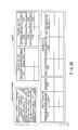
- FIG. 1 is a block diagram schematically showing a memory device according to the embodiment
- FIG. 2 is a block diagram schematically showing part of the arrangement shown in FIG. 1 ;
- FIG. 3 is a flowchart illustrating the operation of an address resolution unit shown in FIG. 2 ;
- FIG. 4 is a flowchart illustrating the operation of a table update unit shown in FIG. 2 ;
- FIG. 5 is a sequence chart schematically showing the operation of data move processing according to the embodiment.
- FIG. 6A is a view showing part of the arrangement in FIG. 2 so as to compare the operation of the embodiment
- FIG. 6B is a view showing an operating state different from that in FIG. 6A ;
- FIG. 6C is a view showing an operating state different from that in FIG. 6B ;
- FIG. 6D is a view showing an operating state different from that in FIG. 6C ;
- FIG. 7A is a view showing part of the arrangement in FIG. 2 so as to indicate the operation of the embodiment
- FIG. 7B is a view showing an operating state different from that in FIG. 7A ;
- FIG. 7C is a view showing an operating state different from that in FIG. 7B ;
- FIG. 8A is a view showing part of the arrangement in FIG. 2 so as to indicate the operation of the embodiment different from those in FIGS. 7A to 7C ;
- FIG. 8B is a view showing an operating state different from that in FIG. 8A ;
- FIG. 8C is a view showing an operating state different from that in FIG. 8B ;
- FIG. 8D is a view showing an operating state different from that in FIG. 8C ;
- FIG. 9A is a view showing part of the arrangement in FIG. 2 so as to indicate the operation of the embodiment different from those in FIGS. 7A to 7C and FIGS. 8A to 8D ;
- FIG. 9B is a view showing an operating state different from that in FIG. 9A ;
- FIG. 9C is a view showing an operating state different from that in FIG. 9B ;
- FIG. 9D is a view showing an operating state different from that in FIG. 9C .
- a memory device includes a memory unit, a first storage unit, a second storage unit, a third storage unit, a data move unit, and a controller.
- the first storage unit stores a logical address and an intermediate address.
- the intermediate address corresponds to the logical address and is used to estimate a physical address of the memory unit.
- the second storage unit stores the intermediate address and the physical address corresponding to the intermediate address.
- the third storage unit stores a flag corresponding to the logical address and the intermediate address. The flag represents whether read of latest data by a read operation using the logical address and the intermediate address has succeeded.
- the data move unit moves data in the memory unit.
- the controller determines whether write has been done for the same logical address of the memory unit during the data move processing, and if the write has been done, invalidates the data move processing.
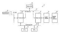
- FIG. 1 is a block diagram showing the schematic arrangement of a memory system according to the embodiment.
- a memory system 11 includes a front end 12 , a back end 13 , a CPU 14 , a CPU 15 , a command system bus (to be referred to as a command bus hereinafter) 16 , a data system bus (to be referred to as a data bus hereinafter) 17 , a data buffer 18 , a NAND channel 19 , a NAND flash memory 20 , and an SAS (Serial Attached SCSI) 21 .
- the front end 12 is controlled by the CPU 14 .
- the front end 12 receives a command, data, and an address from a host device 22 via the SAS 21 , supplies the data to the data buffer 18 via the data bus 17 , and supplies the command and the address to the CPU 14 via the command bus 16 .
- the front end 12 transfers, via the SAS 21 to the host device 22 , data read from the NAND flash memory 20 and held in the data buffer 18 via the NAND channel 19 , the back end 13 , and the data bus 17 .
- the back end 13 is controlled by the CPU 15 .
- the back end 13 has, for example, a command queue which receives a command from the CPU 15 via the command bus 16 .
- the back end 13 receives data from the data buffer 18 via the data bus 17 and transfers the data to the NAND flash memory 20 via the NAND channel 19 .
- the back end 13 receives, via the NAND channel 19 , data read from the NAND flash memory 20 and transfers it to the data buffer 18 via the data bus 17 .
- the back end 13 includes an address resolution unit, a data write/read unit, a table update unit, a scoreboard, and the like and manages the addresses, data, and various kinds of protocols of the NAND flash memory 20 , as will be described later.
- the data buffer 18 is formed from, for example, a RAM (Random Access Memory), and stores data supplied from the front end 12 and the back end 13 via the data bus 17 and also address translation tables to be described later.
- RAM Random Access Memory
- the NAND flash memory 20 has a memory cell array serving as a memory unit having a plurality of memory cells arranged in a matrix, and adopts an address translation method of translating a logical address to a physical address and a write once method of sequentially writing data in a free area on a page-by-page basis. In addition, the NAND flash memory 20 performs data move processing of moving written data to a free area to reduce wasteful free areas.
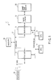
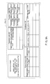
- FIG. 2 shows the schematic functions of the data buffer 18 , the back end 13 , the CPU 15 , and the NAND flash memory 20 ( 800 ).
- the data buffer 18 includes translation tables 600 and 700 serving as first and second storage units, respectively.
- the entire physical memory of the NAND flash memory 20 has a logical address set for every predetermined number of pages (for example, several thousand pages). Some of the logical addresses are stored in the translation table 600 together with intermediate addresses. The intermediate address is used to estimate the physical address.
- a request is issued to the CPU 15 , and the CPU 15 prepares, in the data buffer 18 , a new translation table 600 having free entries.
- the translation table 700 stores intermediate addresses assigned in correspondence with the physical addresses of the NAND flash memory 20 together with the physical addresses. Like the translation table 600 , if all intermediate addresses in the translation table 700 are used up, a request is issued to the CPU 15 , and the CPU 15 prepares a new translation table 700 in the data buffer 18 .
- the back end 13 includes, for example, an address resolution unit 300 , a data write/read unit 400 , a table update unit 500 , and a scoreboard 100 .
- the address resolution unit 300 Upon receiving a write command supplied from the CPU 15 , the address resolution unit 300 translates a logical address supplied together with the write command from an intermediate address to a physical address using the translation tables 600 and 700 .
- the data write/read unit 400 is connected to the address resolution unit 300 and the table update unit 500 so as to control data write/read for the physical memory 800 (NAND flash memory 20 ). More specifically, in accordance with a write command, the data write/read unit 400 writes data, which is held in the data buffer 18 , in the physical memory 800 based on a physical address assigned by the address resolution unit 300 . In addition, the data write/read unit 400 reads data from the physical memory 800 in accordance with a read command. The data write/read unit 400 outputs a signal representing whether the data write or data read for the physical memory 800 has succeeded or not.
- the table update unit 500 is connected to the data write/read unit 400 , the translation tables 600 and 700 , and the scoreboard 100 so as to search the translation tables 600 and 700 in data write/read and update necessary addresses in data write.
- the table update unit 500 also updates the contents of the scoreboard 100 in data read.
- the scoreboard 100 stores intermediate addresses 120 in correspondence with logical addresses 110 and also stores latest data read success flags 130 each representing whether read of latest data has succeeded or not.
- a data move processing unit 200 performs processing of reading already written data and writing the read data in a newly allocated area. For example, when data stored in a storage area (block) is partially rewritten, it is necessary to write the new rewritten data in a new block after erase and also read the remaining unrewritten data from the old block and write it in the new block. The data move processing unit 200 executes such data move processing.
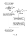
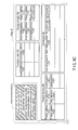
- FIG. 3 illustrates the operation of the address resolution unit 300 in detail.
- the address resolution unit 300 receives a command issued by the CPU 15 when, for example, writing user data, and receives a command issued by the table update unit 500 in data move processing.
- the address resolution unit 300 Upon receiving a supplied command, the address resolution unit 300 determines the command type (S 11 ). If the supplied command is determined to be a write command, the address resolution unit 300 looks up the translation table 700 and assigns an intermediate address and a physical address preset in it to the command in accordance with the command submission order (S 12 ).
- the address resolution unit 300 determines what is the type of the address added to the command, i.e., logical address or physical address (S 13 ). Upon determining that the address is a physical address, the processing ends without address resolution.
- the address resolution unit 300 searches the translation table 600 for a logical address that matches the logical address added to the command, and reads an intermediate address corresponding to the logical address (S 14 ).
- the address resolution unit 300 searches for the translation table 700 for an intermediate address that matches the read intermediate address, and reads a physical address corresponding to the found intermediate address. This physical address is assigned to the input command (S 15 ).
- FIG. 4 illustrates the operation of the table update unit 500 in detail.
- the data write/read unit 400 upon ending the data write or read processing, the data write/read unit 400 outputs a signal representing whether the write has succeeded or not or a signal representing whether the read has succeeded.
- the table update unit 500 operates in accordance with these signals.
- the table update unit 500 first determines the type of the currently supplied command. More specifically, the table update unit 500 determines whether the command is of data move processing (S 21 ). Upon determining that the command is not of data move processing, the table update unit 500 determines whether the supplied command is a read command or a write command (S 22 ). If the command is a read command, the CPU 15 is notified of the end of the processing (S 25 ).
- the table update unit 500 determines the signal representing whether the write has succeeded or not, which is supplied from the data write/read unit 400 (S 23 ). If the write has failed, the CPU 15 is notified of the end of the processing (S 25 ). If the write has succeeded, the table update unit 500 registers the intermediate address used for the write in the entry of the corresponding logical address of the translation table 600 (S 24 ). After that, the CPU 15 is notified of the end of the processing (S 25 ).
- step S 21 if it is determined in step S 21 that the supplied command is a data move processing command, the table update unit 500 determines whether the command is a write command or a read command (S 26 ).
- the table update unit 500 Upon determining that the supplied command is a read command, the table update unit 500 obtains the latest intermediate address from the translation table 600 in accordance with the logical address read from the physical memory 800 (S 27 ). After that, the table update unit 500 obtains the latest physical address from the translation table 700 in accordance with the latest intermediate address obtained from the translation table 600 (S 28 ). Next, the latest physical address obtained from the translation table 700 is compared with the physical address added to the command. If the two physical addresses match, the read of the latest data is determined to have succeeded. If the two physical addresses do not match, the read of the latest data is determined to have failed (S 29 ). Then, the logical address, the latest intermediate address, and the latest read success flag are registered in the scoreboard 100 (S 30 ).
- the latest data read success flag 130 in the scoreboard 100 is set to “1”.
- the latest data read success flag 130 in the scoreboard 100 is set to “0”. After that, a write command is supplied to the address resolution unit 300 (S 31 ).
- step S 26 upon determining in step S 26 that the command is a write command, the table update unit 500 determines the signal representing whether the write has succeeded or not, which is supplied from the data write/read unit 400 after performing a write operation based on the write command (S 32 ). If the write has failed, the CPU 15 is notified of the end of the processing (S 25 ).
- the table update unit 500 obtains the latest intermediate address from the translation table 600 in accordance with the logical address added to the write command (S 33 ). After that, the table update unit 500 searches the scoreboard 100 for the intermediate address at the time of read and the latest read success flag in accordance with the logical address added to the write command (S 34 ). Next, the table update unit 500 determines whether the read latest read success flag is “0” or “1”. If the flag is “0”, the CPU 15 is notified of the end of the processing (S 35 ).
- the latest intermediate address found from the translation table 600 is compared with the intermediate address in the scoreboard 100 (S 36 ). If they match upon comparison, the table update unit 500 registers the intermediate address used for the write in the entry of the corresponding logical address of the translation table 600 in step S 24 (S 24 ). On the other hand, if the two intermediate addresses do not match, the CPU 15 is notified of the end of the processing (S 25 ).
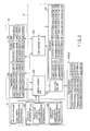
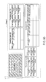
- FIG. 5 shows the schematic operation sequences of the CPU 15 , the address resolution unit 300 , the data write/read unit 400 , and the table update unit 500 shown in FIG. 2 .
- the same reference numbers as in FIGS. 1 and 2 denote the same parts in FIG. 5 .
- the operation of the arrangement in FIG. 2 will schematically be described with reference to FIG. 5 .
- the CPU 15 first submits a write command in the address resolution unit 300 (S 41 ).
- a logical address is added to the write command.
- the address resolution unit 300 obtains a physical address from the translation table 700 given in advance, and assigns it to the write command (S 42 ).
- the address resolution unit 300 supplies the write command with the added physical address to the data write/read unit 400 (S 43 ).
- the data write/read unit 400 writes the data at the corresponding physical address of the physical memory 800 (NAND flash memory 20 ) (S 44 ). At this time, the logical address added to the write command is written to the physical memory 800 as associated information together with the data.
- the data write/read unit 400 notifies the table update unit 500 whether the write has succeeded (S 45 ).
- the table update unit 500 updates the translation table 600 (S 46 ). That is, the intermediate address is recorded in correspondence with the logical address in the translation table 600 .
- the table update unit 500 sends an end notification to the CPU 15 (S 47 ).
- data move processing includes data read and data write processing.
- the data read processing is similar to that by the user. However, although the data read processing by the user uses a logical address, the data read processing in the data move processing uses a physical address.
- the address resolution unit 300 supplies it to the data write/read unit 400 without address resolution, unlike when using a logical address (S 51 and S 52 ).
- the data write/read unit 400 reads data directly from the physical memory 800 based on the physical address (S 53 ). After the read operation, the data write/read unit 400 outputs a signal representing whether the read has succeeded or not (S 54 ).
- the table update unit 500 sets the latest data read success flag 130 in the scoreboard 100 in accordance with the signal (S 55 ).
- the table update unit 500 After that, the table update unit 500 generates a write command and supplies it to the address resolution unit 300 so as to write the read data (S 56 ). That is, the table update unit 500 supplies the write command to the address resolution unit 300 .
- the address resolution unit 300 assigns a physical address corresponding to a free block to the received write command by looking up the translation table 700 (S 57 ), and supplies the physical address and the write command to the data write/read unit 400 (S 58 ).
- the data write/read unit 400 writes the read data in the physical memory 800 in accordance with the write command supplied from the address resolution unit 300 (S 59 ). Then, the data write/read unit 400 outputs a signal representing whether the write has succeeded or not (S 60 ). Upon receiving the signal representing that the write has succeeded from the data write/read unit 400 , the table update unit 500 checks the scoreboard 100 and updates the translation table 600 (S 61 ). More specifically, if the latest data read success flag in the scoreboard 100 represents success, the translation table 600 is updated. After that, the table update unit 500 supplies an end notification to the CPU 15 (S 62 ).
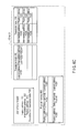
- FIGS. 6A , 6 B, 6 C, and 6 D show a comparative example without using the embodiment.
- This comparative example indicates the states of the translation tables 600 and 700 and the physical memory 800 when the latest data positions contradict because of user write during data move processing.
- data move processing is performed by reading latest data from the physical memory 800 based on a physical read command and then moving the data to new intermediate and physical addresses based on a logical write command.
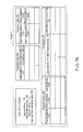
- FIGS. 7A , 7 B, 7 C, and 7 D show data move processing according to the embodiment in detail, indicating the states of the translation tables 600 and 700 , the physical memory 800 , and the scoreboard 100 in the data move processing.
- FIG. 7B shows the state after the physical read command 210 has been executed as part of data move processing.
- the latest read success flag 130 is determined (S 35 in FIG. 4 ).
- the latest read success flag is “1”
- the absence of the user write command interrupt before execution of the physical read command 210 can also be confirmed.
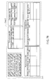
- FIGS. 8A , 8 B, 8 C, and 8 D show a case in which execution of user write before the logical write command of data move processing is detected using the scoreboard 100 when this embodiment is used.
- the user write command is executed in FIG. 8C (step 3 ) between the physical read command 210 of data move processing shown in FIG. 8B (step 2 ) and the logical write command 220 shown in FIG. 8D (step 4 ).
- FIG. 8A (step 1 ) and FIG. 8B (step 2 ) are the same as FIGS. 7A and 7B .
- FIG. 8D shows a state after execution of the logical write command 220 as part of data move processing.
- the latest read success flag is determined (S 35 in FIG. 4 ).
- the latest read success flag 130 is “1”
- the data written by the logical write command 220 is the old data in FIG. 8B (step 2 ).
- the CPU 15 is notified of the processing according to the logical write command 220 without updating the translation table 600 (S 25 in FIG. 4 ).
- the logical write command 220 is invalidated. That is, the data move processing is invalidated.
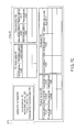
- FIGS. 9A , 9 B, 9 C, and 9 D show a case in which execution of user write before the physical read command of data move processing is detected using the scoreboard when this embodiment is used.
- FIG. 9A (step 1 ) is the same as FIG. 8A .
- FIG. 9B shows a state in which the user write command is executed after the software has calculated the physical address to be used in FIG. 9C (step 3 ).
- FIG. 9C shows a state after the physical read command 210 as part of data move processing has been executed.
- Data position calculation of the physical read command 210 is done by the software before FIG. 9B (step 2 ).
- FIG. 9D shows a state after execution of the logical write command 220 as part of data move processing.
- the scoreboard 100 is provided, and the intermediate address 120 and the latest data read success flag 130 are registered in the scoreboard 100 in correspondence with the logical address 110 . For this reason, in the data move processing, the intermediate address and the latest read success flag 130 registered in the scoreboard 100 are confirmed by the logical write command after execution of the physical read command, thereby confirming whether the user write command has been executed after the execution of the physical read command before the execution of the logical write command. It is therefore unnecessary to prohibit the user write command to the same logical address even during execution of data move processing. Hence, it is possible to prevent the processing speed of the user write command from lowering.
- the latest read success flag is “0”
- the presence of the user write command interrupt before execution of the physical read command 210 can be confirmed.
- the position of the latest data can correctly be managed because the translation table 600 is not updated.
- the latest data read success flag 130 of the scoreboard 100 is set in accordance with the physical read command 210 , the embodiment is not limited to this. For example, it may be set in accordance with the user write command.
- the various modules of the systems described herein can be implemented as software applications, hardware and/or software modules, or components on one or more computers, such as servers. While the various modules are illustrated separately, they may share some or all of the same underlying logic or code.
Landscapes
- Engineering & Computer Science (AREA)
- Theoretical Computer Science (AREA)
- Physics & Mathematics (AREA)
- General Engineering & Computer Science (AREA)
- General Physics & Mathematics (AREA)
- Techniques For Improving Reliability Of Storages (AREA)
- Memory System (AREA)
Abstract
Description
Claims (11)
Applications Claiming Priority (3)
| Application Number | Priority Date | Filing Date | Title |
|---|---|---|---|
| JP2010-268482 | 2010-12-01 | ||
| JP2010268482A JP5323030B2 (en) | 2010-12-01 | 2010-12-01 | Memory device and memory control method |
| JP2010268482 | 2010-12-01 |
Publications (2)
| Publication Number | Publication Date |
|---|---|
| US20120140561A1 US20120140561A1 (en) | 2012-06-07 |
| US8856468B2 true US8856468B2 (en) | 2014-10-07 |
Family
ID=46162120
Family Applications (1)
| Application Number | Title | Priority Date | Filing Date |
|---|---|---|---|
| US13/278,973 Active 2033-04-05 US8856468B2 (en) | 2010-12-01 | 2011-10-21 | Memory device capable of improving write processing speed and memory control method |
Country Status (2)
| Country | Link |
|---|---|
| US (1) | US8856468B2 (en) |
| JP (1) | JP5323030B2 (en) |
Cited By (1)
| Publication number | Priority date | Publication date | Assignee | Title |
|---|---|---|---|---|
| US11176032B2 (en) * | 2019-08-28 | 2021-11-16 | Kioxia Corporation | Memory system and method of controlling nonvolatile memory |
Families Citing this family (3)
| Publication number | Priority date | Publication date | Assignee | Title |
|---|---|---|---|---|
| JP6180271B2 (en) * | 2013-10-09 | 2017-08-16 | 日本放送協会 | Video recording apparatus and video recording method |
| CN105353989B (en) * | 2015-11-19 | 2018-12-28 | 华为技术有限公司 | Storing data access method and relevant controller, equipment, host and system |
| KR20200143871A (en) * | 2019-06-17 | 2020-12-28 | 삼성전자주식회사 | Electronic device including storage and method of using the storage thereof |
Citations (9)
| Publication number | Priority date | Publication date | Assignee | Title |
|---|---|---|---|---|
| JPS6375948A (en) | 1986-09-19 | 1988-04-06 | Fujitsu Ltd | Garbage collection control system |
| JPS6393055A (en) | 1986-10-07 | 1988-04-23 | Fujitsu Ltd | Real time type garbage collection back-up device |
| US5400337A (en) * | 1992-04-06 | 1995-03-21 | Northern Telecom Limited | Method for ATM switch core interface |
| JP2001184254A (en) | 1999-12-27 | 2001-07-06 | Nec Corp | Information processor having garbage collection function, and method for the same, and recording medium |
| JP2001265750A (en) | 2000-03-17 | 2001-09-28 | Omron Corp | Memory controller |
| US6725322B1 (en) * | 1999-02-22 | 2004-04-20 | Renesas Technology Corp. | Memory card, method for allotting logical address, and method for writing data |
| JP2006172495A (en) | 1997-11-21 | 2006-06-29 | Omron Corp | Program control apparatus and method, and program recording medium |
| US7511646B2 (en) * | 2006-05-15 | 2009-03-31 | Apple Inc. | Use of 8-bit or higher A/D for NAND cell value |
| US8099730B2 (en) * | 2006-03-30 | 2012-01-17 | Intel Corporation | Heterogeneous virtualization of host and guest OS having different register sizes using translation layer to extract device port numbers for host OS system memory addresses |
-
2010
- 2010-12-01 JP JP2010268482A patent/JP5323030B2/en active Active
-
2011
- 2011-10-21 US US13/278,973 patent/US8856468B2/en active Active
Patent Citations (9)
| Publication number | Priority date | Publication date | Assignee | Title |
|---|---|---|---|---|
| JPS6375948A (en) | 1986-09-19 | 1988-04-06 | Fujitsu Ltd | Garbage collection control system |
| JPS6393055A (en) | 1986-10-07 | 1988-04-23 | Fujitsu Ltd | Real time type garbage collection back-up device |
| US5400337A (en) * | 1992-04-06 | 1995-03-21 | Northern Telecom Limited | Method for ATM switch core interface |
| JP2006172495A (en) | 1997-11-21 | 2006-06-29 | Omron Corp | Program control apparatus and method, and program recording medium |
| US6725322B1 (en) * | 1999-02-22 | 2004-04-20 | Renesas Technology Corp. | Memory card, method for allotting logical address, and method for writing data |
| JP2001184254A (en) | 1999-12-27 | 2001-07-06 | Nec Corp | Information processor having garbage collection function, and method for the same, and recording medium |
| JP2001265750A (en) | 2000-03-17 | 2001-09-28 | Omron Corp | Memory controller |
| US8099730B2 (en) * | 2006-03-30 | 2012-01-17 | Intel Corporation | Heterogeneous virtualization of host and guest OS having different register sizes using translation layer to extract device port numbers for host OS system memory addresses |
| US7511646B2 (en) * | 2006-05-15 | 2009-03-31 | Apple Inc. | Use of 8-bit or higher A/D for NAND cell value |
Non-Patent Citations (1)
| Title |
|---|
| Japanese Office Action mailed on Apr. 9, 2013 in connection with Application No. 2010-268482. |
Cited By (3)
| Publication number | Priority date | Publication date | Assignee | Title |
|---|---|---|---|---|
| US11176032B2 (en) * | 2019-08-28 | 2021-11-16 | Kioxia Corporation | Memory system and method of controlling nonvolatile memory |
| US11720487B2 (en) | 2019-08-28 | 2023-08-08 | Kioxia Corporation | Memory system and method of controlling nonvolatile memory |
| US20230333980A1 (en) * | 2019-08-28 | 2023-10-19 | Kioxia Corporation | Memory system and method of controlling nonvolatile memory |
Also Published As
| Publication number | Publication date |
|---|---|
| JP2012118797A (en) | 2012-06-21 |
| US20120140561A1 (en) | 2012-06-07 |
| JP5323030B2 (en) | 2013-10-23 |
Similar Documents
| Publication | Publication Date | Title |
|---|---|---|
| US10915475B2 (en) | Methods and apparatus for variable size logical page management based on hot and cold data | |
| US8762661B2 (en) | System and method of managing metadata | |
| US7953953B2 (en) | Method and apparatus for reducing page replacement time in system using demand paging technique | |
| US8510502B2 (en) | Data writing method, and memory controller and memory storage apparatus using the same | |
| US10579267B2 (en) | Memory controller and memory system | |
| US8825946B2 (en) | Memory system and data writing method | |
| JP6139381B2 (en) | Memory system and method | |
| US20150012687A1 (en) | Method for managing commands in command queue, memory control circuit unit and memory storage apparatus | |
| US20190146908A1 (en) | Method for accessing flash memory module and associated flash memory controller and electronic device | |
| US20140223075A1 (en) | Physical-to-logical address map to speed up a recycle operation in a solid state drive | |
| TW202028982A (en) | Data storage device and method for accessing logical-to-physical mapping table | |
| CN113272903B (en) | Handling operation conflicts in non-volatile memory | |
| US20170160940A1 (en) | Data processing method and apparatus of solid state disk | |
| US8856468B2 (en) | Memory device capable of improving write processing speed and memory control method | |
| US10025706B2 (en) | Control device, storage device, and storage control method | |
| US20160070648A1 (en) | Data storage system and operation method thereof | |
| US9329994B2 (en) | Memory system | |
| US11836092B2 (en) | Non-volatile storage controller with partial logical-to-physical (L2P) address translation table | |
| US20170199687A1 (en) | Memory system and control method | |
| US20200192810A1 (en) | Data Storage Devices and Data Processing Methods | |
| CN111831589A (en) | Method and device for improving IO command processing parallelism | |
| CN112447227A (en) | Command tracking | |
| US7996598B2 (en) | Memory management module | |
| US20190361803A1 (en) | Logical-to-physical table updating method and storage controller |
Legal Events
| Date | Code | Title | Description |
|---|---|---|---|
| AS | Assignment |
Owner name: KABUSHIKI KAISHA TOSHIBA, JAPAN Free format text: ASSIGNMENT OF ASSIGNORS INTEREST;ASSIGNOR:FUKUDA, TOHRU;REEL/FRAME:027128/0648 Effective date: 20110829 |
|
| STCF | Information on status: patent grant |
Free format text: PATENTED CASE |
|
| FEPP | Fee payment procedure |
Free format text: PAYOR NUMBER ASSIGNED (ORIGINAL EVENT CODE: ASPN); ENTITY STATUS OF PATENT OWNER: LARGE ENTITY |
|
| AS | Assignment |
Owner name: TOSHIBA MEMORY CORPORATION, JAPAN Free format text: ASSIGNMENT OF ASSIGNORS INTEREST;ASSIGNOR:KABUSHIKI KAISHA TOSHIBA;REEL/FRAME:043709/0035 Effective date: 20170706 |
|
| MAFP | Maintenance fee payment |
Free format text: PAYMENT OF MAINTENANCE FEE, 4TH YEAR, LARGE ENTITY (ORIGINAL EVENT CODE: M1551) Year of fee payment: 4 |
|
| AS | Assignment |
Owner name: K.K. PANGEA, JAPAN Free format text: MERGER;ASSIGNOR:TOSHIBA MEMORY CORPORATION;REEL/FRAME:055659/0471 Effective date: 20180801 Owner name: KIOXIA CORPORATION, JAPAN Free format text: CHANGE OF NAME AND ADDRESS;ASSIGNOR:TOSHIBA MEMORY CORPORATION;REEL/FRAME:055669/0001 Effective date: 20191001 Owner name: TOSHIBA MEMORY CORPORATION, JAPAN Free format text: CHANGE OF NAME AND ADDRESS;ASSIGNOR:K.K. PANGEA;REEL/FRAME:055669/0401 Effective date: 20180801 |
|
| MAFP | Maintenance fee payment |
Free format text: PAYMENT OF MAINTENANCE FEE, 8TH YEAR, LARGE ENTITY (ORIGINAL EVENT CODE: M1552); ENTITY STATUS OF PATENT OWNER: LARGE ENTITY Year of fee payment: 8 |