US8854440B2 - Three dimensional image display device and a method of driving the same - Google Patents
Three dimensional image display device and a method of driving the same Download PDFInfo
- Publication number
- US8854440B2 US8854440B2 US13/197,289 US201113197289A US8854440B2 US 8854440 B2 US8854440 B2 US 8854440B2 US 201113197289 A US201113197289 A US 201113197289A US 8854440 B2 US8854440 B2 US 8854440B2
- Authority
- US
- United States
- Prior art keywords
- voltage
- reset signal
- gate
- high level
- time
- Prior art date
- Legal status (The legal status is an assumption and is not a legal conclusion. Google has not performed a legal analysis and makes no representation as to the accuracy of the status listed.)
- Active, expires
Links
Images


Classifications
-
- H04N13/0497—
-
- G—PHYSICS
- G02—OPTICS
- G02B—OPTICAL ELEMENTS, SYSTEMS OR APPARATUS
- G02B30/00—Optical systems or apparatus for producing three-dimensional [3D] effects, e.g. stereoscopic images
- G02B30/20—Optical systems or apparatus for producing three-dimensional [3D] effects, e.g. stereoscopic images by providing first and second parallax images to an observer's left and right eyes
- G02B30/22—Optical systems or apparatus for producing three-dimensional [3D] effects, e.g. stereoscopic images by providing first and second parallax images to an observer's left and right eyes of the stereoscopic type
- G02B30/24—Optical systems or apparatus for producing three-dimensional [3D] effects, e.g. stereoscopic images by providing first and second parallax images to an observer's left and right eyes of the stereoscopic type involving temporal multiplexing, e.g. using sequentially activated left and right shutters
-
- G—PHYSICS
- G09—EDUCATION; CRYPTOGRAPHY; DISPLAY; ADVERTISING; SEALS
- G09G—ARRANGEMENTS OR CIRCUITS FOR CONTROL OF INDICATING DEVICES USING STATIC MEANS TO PRESENT VARIABLE INFORMATION
- G09G3/00—Control arrangements or circuits, of interest only in connection with visual indicators other than cathode-ray tubes
- G09G3/20—Control arrangements or circuits, of interest only in connection with visual indicators other than cathode-ray tubes for presentation of an assembly of a number of characters, e.g. a page, by composing the assembly by combination of individual elements arranged in a matrix no fixed position being assigned to or needed to be assigned to the individual characters or partial characters
- G09G3/34—Control arrangements or circuits, of interest only in connection with visual indicators other than cathode-ray tubes for presentation of an assembly of a number of characters, e.g. a page, by composing the assembly by combination of individual elements arranged in a matrix no fixed position being assigned to or needed to be assigned to the individual characters or partial characters by control of light from an independent source
- G09G3/3406—Control of illumination source
-
- H04N13/0438—
-
- H—ELECTRICITY
- H04—ELECTRIC COMMUNICATION TECHNIQUE
- H04N—PICTORIAL COMMUNICATION, e.g. TELEVISION
- H04N13/00—Stereoscopic video systems; Multi-view video systems; Details thereof
- H04N13/30—Image reproducers
- H04N13/302—Image reproducers for viewing without the aid of special glasses, i.e. using autostereoscopic displays
- H04N13/32—Image reproducers for viewing without the aid of special glasses, i.e. using autostereoscopic displays using arrays of controllable light sources; using moving apertures or moving light sources
-
- H—ELECTRICITY
- H04—ELECTRIC COMMUNICATION TECHNIQUE
- H04N—PICTORIAL COMMUNICATION, e.g. TELEVISION
- H04N13/00—Stereoscopic video systems; Multi-view video systems; Details thereof
- H04N13/30—Image reproducers
- H04N13/332—Displays for viewing with the aid of special glasses or head-mounted displays [HMD]
- H04N13/337—Displays for viewing with the aid of special glasses or head-mounted displays [HMD] using polarisation multiplexing
-
- H—ELECTRICITY
- H04—ELECTRIC COMMUNICATION TECHNIQUE
- H04N—PICTORIAL COMMUNICATION, e.g. TELEVISION
- H04N13/00—Stereoscopic video systems; Multi-view video systems; Details thereof
- H04N13/30—Image reproducers
- H04N13/332—Displays for viewing with the aid of special glasses or head-mounted displays [HMD]
- H04N13/341—Displays for viewing with the aid of special glasses or head-mounted displays [HMD] using temporal multiplexing
-
- H—ELECTRICITY
- H04—ELECTRIC COMMUNICATION TECHNIQUE
- H04N—PICTORIAL COMMUNICATION, e.g. TELEVISION
- H04N13/00—Stereoscopic video systems; Multi-view video systems; Details thereof
- H04N13/30—Image reproducers
- H04N13/398—Synchronisation thereof; Control thereof
Definitions
- the present invention relates to a three dimensional (3D) image display device and a method of driving the same.
- a 3D image display technique allows a viewer to feel the depth (e.g., a 3D effect) of an object by using binocular parallax.
- Binocular parallax may exist due to the eyes of a person being spaced apart from each other by a predetermined distance, and thus, a two dimensional (2D) image seen in the left eye is different from that seen in the right eye.
- 2D two dimensional
- Techniques for displaying 3D images may be classified into a stereoscopic method and an autostereoscopic method.
- the stereoscopic method uses shutter glasses or polarized glasses and the autostereoscopic method does not use glasses, but instead arranges a lenticular lens and a parallax barrier in a display panel.
- an image to be seen in the left eye and an image to be seen in the right eye image are separately and continuously output from a display panel to a pair of shutter glasses and the left eye shutter and the right eye shutter of the shutter glass are selectively opened and closed, thereby displaying 3D images.
- shutter glasses are impacted by crosstalk. This refers to the ghosting of images when the right eye sees some residue of the image intended for the left eye and vice versa. Accordingly, there is a need to reduce crosstalk in shutter glasses.
- An exemplary embodiment of the present invention provides a three dimensional image display device, including: a display panel that alternately displays a left eye image and a right eye image, wherein a common voltage synchronized with a voltage reset signal is applied to the display panel and the voltage reset signal is maintained at a high level for a predetermined time before the left eye image or the right eye image is input.
- the common voltage may be a reference common voltage, a first voltage in which a reset voltage is added to the reference common voltage, or a second voltage in which the reset voltage is subtracted from the reference common voltage.
- the first voltage or the second voltage as the common voltage may be maintained at a high level while the voltage reset signal is maintained at a high level.
- a gate-on voltage may be applied to a plurality of gate lines based on at least one of the voltage reset signal and a gate reset signal.
- the gate-on voltage may be simultaneously applied to the plurality of gate lines while at least one of the voltage reset signal and the gate reset signal is maintained at a high level.
- the gate-on voltage may be sequentially applied to the plurality of gate lines while at least one of the voltage reset signal and the gate reset signal is maintained at a low level.
- a left eye shutter may maintain an open state from a time when an input of the left eye image starts to a time when an application of a first pulse of the voltage reset signal starts and a right eye shutter may maintain an open state from a time when an input of the right eye image starts to a time when an application of a second pulse of the voltage reset signal starts, based on a 3D sync signal.
- the right eye shutter may maintain a closed state from a time when an application of a third pulse of the voltage reset signal starts to a time when an application of a first pulse of the voltage reset signal ends and the left eye shutter may maintain a closed state from a time when an application of the first pulse of the voltage reset signal starts to a time when an application of a second pulse of the voltage reset signal ends, based on the 3D sync signal.
- the three dimensional image display device may further include a backlight unit, wherein the backlight unit may be turned-on from a time when an input of the left eye image starts to a time when an application of a first pulse of the voltage reset signal starts, and the backlight unit may be turned-on from a time when an input of the right eye image starts to a time when an application of the second pulse of the voltage reset signal starts.
- the backlight unit may be turned-off for a time when the voltage reset signal is maintained at a high level.
- the display panel displays black for a predetermined time.
- the predetermined time may be about 0.5 ms or less.
- the three dimensional image display device may further include: a common voltage switching unit that switches the common voltage based on the voltage reset signal.
- the three dimensional image display device may further include a gate-on voltage switching unit that applies a gate-on voltage to a plurality of gate lines based on at least one of the voltage reset signal and a gate reset signal.
- the gate-on voltage switching unit may include a first output terminal and a second output terminal and the first output terminal may be connected to the plurality of gate lines and the second output terminal may be connected to a gate driver.
- Another exemplary embodiment of the present invention provides a method of driving a three dimensional display device, the method including: alternately displaying a left eye image and a right eye image in a display panel; and applying a common voltage synchronized with a voltage reset signal to the display panel, wherein the voltage reset signal is maintained at a high level for a predetermined time before the left eye image or the right eye image is input.
- An exemplary embodiment of the present invention provides, a 3D image display device, including: a display panel that alternately displays a first eye image and a second eye image, wherein after the first eye image is displayed and before the second eye image displayed, a common voltage of a first level may be applied to the display panel for a predetermined time, wherein the first level of the common voltage causes about the entire display panel to display black for the predetermined time.
- the first level of the common voltage may be maintained for the predetermined time by a voltage reset signal.
- the first level of the common voltage may be changed to a second level by the voltage reset signal immediately before the second eye image is displayed, wherein the second level causes about the entire display panel to stop displaying black.
- FIG. 1 is a diagram showing an operation of a three dimensional (3D) image display device according to an exemplary embodiment of the present invention.
- FIG. 2 is a diagram showing a 3D image display device according to an exemplary embodiment of the present invention.
- FIG. 3 is a diagram showing an operation timing of a 3D image display device according to an exemplary embodiment of the present invention.
- FIG. 4 is a diagram showing a method of applying a common voltage in a 3D image display device according to an exemplary embodiment of the present invention.
- FIG. 5 is a diagram showing a circuit unit for applying a common voltage in a 3D image display device according to an exemplary embodiment of the present invention.
- FIG. 6 is a diagram showing a method of applying a gate-on voltage in a 3D image display device according to an exemplary embodiment of the present invention.
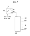
- FIG. 7 is a diagram showing a circuit unit for applying a gate-on voltage in a 3D image display device according to an exemplary embodiment of the present invention.
- FIGS. 1 to 3 a three dimensional (3D) image display device according to an exemplary embodiment of the present invention will be described in detail with reference to FIGS. 1 to 3 .
- FIG. 1 is a diagram showing an operation of a 3D image display device according to an exemplary embodiment of the present invention
- FIG. 2 is a diagram showing a 3D image display device according to an exemplary embodiment of the present invention
- FIG. 3 is a diagram showing an operation timing of a 3D image display device according to an exemplary embodiment of the present invention.
- a shutter member 300 may be a pair of eyeglass-shaped shutter glasses 30 , but is not limited thereto and may instead be a pair of mechanical shutter glasses (e.g., goggles).
- the shutter glasses 30 have right eye shutters 32 and 32 ′ and left eye shutters 31 and 31 ′ which alternately block light at a predetermined cycle depending on the operation of a display panel 100 .
- the right eye shutter may be closed 32 or open 32 ′ and the left eye shutter may be open 31 or closed 31 ′.
- the left eye shutter may be closed 31 ′, when the right eye shutter is open 32 ′ during frame F(N+1), and the right eye shutter may be closed 32 , when the left eye shutter is open 31 during frame F(N).
- left eye shutter and the right eye shutter may be open at the same time or closed at the same time.
- the shutters of the shutter glasses 30 may be formed by the technologies used for making a liquid crystal display, organic light emitting diode display, and electrophoretic display, but are not limited thereto.
- the shutters of the shutter glasses 30 may include two transparent conductive layers and a liquid crystal layer therebetween.
- a polarization film may be disposed on a surface of the conductive layers.
- the liquid crystal substances e.g., liquid crystal molecules
- the shutters may be open or closed due to the rotation.
- the left eye shutter 31 of the shutter glasses 30 is open to transmit the images 101 and 102 to the left eye, and the right eye shutter 32 of the shutter glasses 30 is closed to block the images 101 and 102 from the right eye.
- the right eye shutter 32 ′ of the shutter glasses 30 is open to transmit the images 101 ′ and 102 ′ to the right eye, and the left eye shutter 31 ′ of the shutter glasses 30 is closed to block the images 101 ′ and 102 ′ from the left eye.
- the left eye image is seen by only the left eye for a predetermined time and then the right eye image is seen by only the right eye for a predetermined time, such that an image having depth perception (e.g., a 3D image) is seen due to a difference between the left eye image and the right eye image.
- an image having depth perception e.g., a 3D image
- the image seen by the left eye is an image in which the quadrangle of the left eye image 101 and the triangle of the left eye image 102 are separated by a distance ⁇ from each other.
- the image seen by the right eye is an image in which the quadrangle of the right eye image 101 ′ and the triangle of the right eye image 102 ′ are separated by a distance ⁇ from each other.
- the ⁇ and ⁇ may have different values from each other.
- the quadrangles appear closer to the wearer of the shutter glasses 30 and the triangles appear behind the quadrangles to the wearer of the shutter glasses 30 , thereby giving depth to these objects.
- the direction of the arrows shown in the display panel 100 shows the order in which a gate-on voltage Von is applied to a plurality of gate lines extending substantially in the row direction across the display panel 100 .
- the gate-on signal Von may be sequentially applied from the upper gate line to the lower gate line in the display panel 100 .
- the display panel 100 may display the left eye images 101 and 102 , as follows.
- the gate-on voltage Von is sequentially applied from the upper row of the gate lines to the lower row of the gate lines such that, for a gate line row receiving the gate-on voltage Von, a data voltage is applied to pixel electrodes of that row through thin film transistors connected to that gate line.
- the applied data voltage is a data voltage for displaying the left eye images 101 and 102 (which may hereinafter be, referred to as “left eye data voltage”) and the applied left eye data voltage may be kept for a predetermined time by a storage capacitor in individual pixels.
- a data voltage for displaying the right eye images 101 ′ and 102 ′ (which may hereinafter be, referred to as “right eye data voltage”) is then applied so that the display panel 100 may display the right eye images 101 ′ and 102 ′ and the data voltage may be kept for a predetermined time by a storage capacitor in individual pixels.
- the display panel 100 is a liquid crystal display.
- the display panel 100 may include an upper substrate, a lower substrate, and a liquid crystal layer injected between the upper substrate and the lower substrate.
- the display panel 100 displays an image by changing the alignment direction of liquid crystal molecules in the liquid crystal layer, by an electric field generated between two electrodes formed on the upper and lower substrates, respectively, to adjust polarization of light.
- Gate lines GL 1 -GLn, data lines DL 1 -DLm, pixel electrodes, and thin film transistors 105 connected to the gate lines GL 1 -GLn and the data lines DL 1 -DLm are disposed on the lower substrate.
- the thin film transistors 105 respectively control voltage applied to the pixel electrodes on the basis of signals supplied to the gate lines GL 1 -GLn and the data lines DL 1 -DLm.
- the pixel electrodes may be transflective pixel electrodes with a transmissive region and a reflective region.
- storage capacitors 107 may be formed to keep the voltage applied to the pixel electrodes for a predetermined time.
- one pixel 103 may include the thin film transistor 105 , the storage capacitor 107 , and a liquid crystal capacitor 109 .
- a black matrix, a color filter, and a common electrode may be disposed on the upper substrate opposite to the lower substrate.
- a common voltage Vcom is applied to the common electrode.
- At least one of the color filter, the black matrix, and the common electrode formed on the upper substrate may be formed on the lower substrate, and when the common electrode and the pixel electrode are formed on the lower substrate, at least one of the common electrode and the pixel electrode may be a linear electrode.
- the liquid crystal layer may include a liquid crystal of a twisted nematic (TN) mode, a liquid crystal of a vertically aligned (VA) mode, and a liquid crystal of an electrically controlled birefringence (ECB) mode.
- TN twisted nematic
- VA vertically aligned
- EBC electrically controlled birefringence
- a polarizer is attached to the outer surface of the upper substrate and the outer surface of the lower substrate, respectively.
- a compensation film may be disposed between the outer substrate and the polarizer and between the inner substrate and the polarizer.
- a backlight unit 200 includes a light source, and for example, the light source is a fluorescent lamp, such as a cold cathode fluorescent lamp (CCFL), or a light emitting diode (LED).
- a fluorescent lamp such as a cold cathode fluorescent lamp (CCFL), or a light emitting diode (LED).
- CCFL cold cathode fluorescent lamp
- LED light emitting diode
- the backlight unit 200 may include a reflector, a light guide, and a luminance improving film.
- a display apparatus 50 may include the display panel 100 , the backlight unit 200 , a data driver 140 , a gate driver 120 , an image signal processor 160 , a gamma voltage generator 190 , a luminance controller 210 , the shutter member 300 , a frame memory 310 , a frame conversion controller 330 , and a stereo controller 400 .
- the stereo controller 400 may transmit a 3D timing signal and 3D enable signal 3D_En to the luminance controller 210 .
- the luminance controller 210 may transmit a backlight control signal to the backlight unit 200 in response to the 3D timing signal and the 3D enable signal 3D_En.
- the backlight unit 200 may be turned on/off by the backlight control signal from the luminance controller 210 .
- the backlight control signal transmitted to the backlight unit 200 may keep the backlight unit 200 turned on for a predetermined time.
- the backlight control signal may also turn off the backlight unit 200 .
- the stereo controller 400 may transmit a 3D sync signal 3D_sync to the shutter member 300 and the frame conversion controller 330 .
- the shutter member 300 may be electrically connected with the stereo controller 400 .
- the shutter member 300 may receive the 3D sync signal 3D_sync by wireless infrared communication or by a wired connection.
- the shutter member 300 may operate in response to the 3D sync signal 3D_sync or a transformed 3D sync signal.
- the 3D sync signal 3D_sync may include all the signals that are used to open/close the left eye shutter or the right eye shutter of the shutter member 300 .
- the frame conversion controller 330 may transmit control signals PCS and BIC to the image signal processor 160 and the data driver 140 , respectively.
- the stereo controller 400 may receive graphic data and transmit display data DATA in response thereto.
- the stereo controller 400 may also transmit the 3D enable signal 3D_En, and other control signals CONT 1 to the image signal processor 160 .
- the image signal processor 160 may transmit various types of display data DATA′ and various types of control signals CONT 2 , CONT 3 , and CONT 4 to the display panel 100 , through the gate driver 120 , the data driver 140 , and the gamma voltage generator 190 , to display an image on the display panel 100 .
- the gate driver 120 receives the gate-on voltage Von and a gate-off voltage Voff.
- the display data DATA may include left eye image data and right eye image data, or the like, in the 3D image display device.
- the display data DATA may include data suitable for two-dimensional (2D) image viewing when the 3D mode of the 3D image display device is not active.
- left eye image data L 1 and L 2 and right eye image data R 1 are input to the display panel 100 .
- the left eye and right eye image data L 1 , L 2 and R 2 may be a signal represented in digital or analog fashion to effectuate the output of an image (e.g., video or picture) from the display panel 100 .
- an image e.g., video or picture
- a vertical blank (VB) interval when for example, after all the left eye image data L 1 have been input and before the right eye image data R 1 are input or after all the right eye image data R 1 have been input and before the left eye image data L 2 are input; this time is referred to as a vertical blank (VB) interval.
- the VB interval may be about 10% to about 60% of one frame, but is not limited thereto.
- a voltage reset signal Vcom Reset is applied before the left eye image data L 1 , the right eye image data R 1 or the left eye image data L 2 is input to the display panel 100 .
- the voltage reset signal Vcom Reset may be applied immediately before the left eye image data L 1 , the right eye image data R 1 , or the left eye image data L 2 is input to the display panel 100 .
- the common voltage Vcom applied to the display panel 100 is synchronized with the voltage reset signal Vcom Reset.
- the common voltage Vcom may be Vc+Vr or Vc ⁇ Vr.
- Vc+Vr and Vc ⁇ Vr are high voltages that may change all the gray values of the plurality of pixels 103 of the display panel 100 into black. It is noted, however, that these voltages could be changed to change all the gray values of the plurality of pixels 103 of the display panel 100 into white.
- Vcom Reset While the voltage reset signal Vcom Reset is at a low level, the common voltage Vcom is Vc.
- Vc is referred to as a reference common voltage and Vr is referred to as a reset voltage.
- Vc+Vr may be applied, Vc ⁇ Vr may be applied, or Vc+Vr and Vc ⁇ Vr may be alternately applied while the common voltage Vcom is synchronized with the voltage reset signal Vcom Reset.
- Vc+Vr or Vc ⁇ Vr When Vc+Vr or Vc ⁇ Vr is applied to the display panel 100 as the common voltage Vcom, the display panel 100 displays black for a period in which Vc+Vr or Vc ⁇ Vr is applied, thereby reducing a crosstalk phenomenon between the left eye image and the right eye image.
- the black image is displayed on the entire screen of the display panel 100 , thereby reducing the crosstalk phenomenon between the left eye image and the right eye image.
- the black image may be displayed on the entire screen of the display panel 100 .
- a circuit unit for applying the common voltage Vcom may include a common voltage switching unit 150 that switches the common voltage Vcom by the voltage reset signal Vcom Reset.
- the common voltage switching unit 150 applies Vc, Vc+Vr, or Vc ⁇ Vr as the common voltage Vcom, based on the voltage reset signal Vcom Reset.
- Vc+Vr or Vc ⁇ Vr may be applied as the common voltage Vcom and while the voltage reset signal Vcom Reset is at a low level, Vc may be applied as the common voltage Vcom.
- the left eye shutter may be in a closed state CLOSE when a first voltage reset signal Vcom Reset of a high level is applied just before the left image data L 1 is input.
- the left eye shutter may be in an open state OPEN when the left eye image data L 1 is input.
- the left eye shutter may remain in the open state OPEN until a second voltage reset signal Vcom Reset of a high level is applied just before the right eye image data R 1 is input.
- the second voltage reset signal Vcom Reset of a high level is applied the left eye shutter goes into the closed state CLOSE.
- the left eye shutter may remain in the closed state CLOSE until a third voltage reset signal Vcom Reset of a high level goes low just before the left eye image data L 2 is input, at which time the left eye shutter goes back to the open state OPEN.
- the right eye shutter may be in a closed state CLOSE when the first voltage reset signal Vcom Reset of a high level is applied just before the left eye image data L 1 is input.
- the right eye shutter may remain in the closed state CLOSE while the left eye image data L 1 is input and while the second voltage reset signal Vcom Reset of a high level is input just before the right eye image data R 1 is input.
- the right eye shutter may be in an open state OPEN when the right eye image data R 1 is input and may remain in the open state OPEN until the third voltage reset signal Vcom Reset of a high level is input just before the left image data L 2 is input.
- the right eye shutter may go into a closed state CLOSE and may remain there while the left eye image data L 2 is input.
- the luminance of the 3D display device, according to an exemplary embodiment of the present invention, seen through the shutter member 300 may be increased.
- the backlight unit 200 may be turned-on between the consecutive voltage reset signals Vcom Reset of a high level and the luminance of the 3D display device may be increased since the turn-on time of the backlight unit 200 is increased.
- the backlight unit 200 may be turned-on from the time when the voltage reset signal Vcom Reset is changed from a high level to a low level to the time when the voltage reset signal Vcom Reset is changed from a low level to a high level.
- the gate-on voltage Von may be applied to a plurality of gate lines GL 1 to GLn, based on at least one of the voltage reset signal Vcom Reset and a gate reset signal Gate Reset.
- the gate-on voltage Von may be applied to the plurality of gate lines GL 1 to GLn while at least one of the voltage reset signal Vcom Reset and the gate reset signal Gate Reset is maintained at a high level.
- the gate-on voltage Von may be sequentially applied to the plurality of gate lines GL 1 to GLn while at least one of the voltage reset signal Vcom Reset and the gate reset signal Gate Reset is maintained at a low level.
- the gate reset signal Gate Reset for simultaneously applying the gate-on voltage Von to the plurality of gate lines GL 1 to GLn may be synchronized with the voltage reset signal Vcom Reset.
- the gate reset signal Gate Reset may be at a high level.
- the gate-on voltage Von may be almost simultaneously applied to the plurality of gate lines GL 1 to GLn while the gate reset signal Gate Reset is at a high level, such that the plurality of pixel rows of the 3D image display device, according to an exemplary embodiment of the present invention, may almost simultaneously display black.
- the gate-on voltage Von may be sequentially applied to the plurality of gate lines GL 1 to GLn from when the gate reset signal Gate Reset is changed from a high level to a low level.
- the gate reset signal Gate Reset may be omitted.
- the voltage reset signal Vcom Reset may be used instead of the gate reset signal Gate Reset.
- a circuit unit for applying the gate-on voltage Von may include a gate-on voltage switching unit 170 that switches the gate-on voltage Von by the gate reset signal Gate Reset.
- the gate-on voltage switching unit 170 includes a first output terminal OUT 1 and a second output terminal OUT 2 , wherein the first output terminal OUT 1 is connected to the plurality of gate lines GL 1 to GLn and the second output terminal OUT 2 is connected to the gate driver 120 .
- the gate-on voltage switching unit 170 applies the gate-on voltage Von to the gate driver 120 or the plurality of gate lines GL 1 to GLn, based on the gate reset signal Gate Reset.
- the gate-on voltage Von may be almost simultaneously applied to the plurality of gate lines GL 1 to GLn while the gate reset signal Gate Reset is at a high level and the gate-on voltage Von may be applied to the gate driver 120 while the gate reset signal Gate Reset is at a low level.
- the voltage reset signal Vcom Reset may be applied to the gate-on voltage switching unit 170 , instead of the gate reset signal Gate Reset.
- the gate-on voltage Von may be almost simultaneously applied to the plurality of gate lines GL 1 to GLn while the voltage reset signal Vcom Reset is at a high level and the gate-on voltage Von may be applied to the gate driver 120 while the voltage reset signal Vcom Reset is at a low level.
- the gate driver 120 may be mounted in the display panel 100 and may include a plurality of stages that are dependently connected with each other.
- the stages may receive various control signals CONT 2 from the image signal processor 160 .
- control signal CONT 2 may include a scan start signal, or the like.
- control signal CONT 2 may include a clock signal, a low voltage signal, or the like.
- a response speed of its liquid crystal when going from white-to-black is faster than that when going from black-to-white.
- the response speed of the TN-type liquid crystal molecules when going from white-to-black may be about 1 ms or less and the response speed of the TN-type liquid crystal molecules when going from black-to-white may be about 3 ms or more.
- the average response speed of the TN-type liquid crystal molecules that change from black to a target gray value may be faster than that of the TN-type liquid crystal molecules that change from white to a target gray value.
- the left eye image or the right eye image is displayed after displaying black on the screen of the TN-type liquid crystal display rather than displaying the left eye image or the right eye image after displaying white on the screen thereof.
- the visibility of a moving picture may be improved due to the improvement of the response speed of the liquid crystal molecules.
- Vc+Vr may be applied to the liquid crystal display as the common voltage Vcom so that the positive data voltage and the negative data voltage are changed into positive black data voltage.
- Vc ⁇ Vr may be applied to the liquid crystal display as the common voltage Vcom so that the positive data voltage and the negative data voltage are changed into the negative black data voltage.
- Vc+Vr and Vc ⁇ Vr may be alternately applied to the liquid crystal display as the common voltage Vcom so that the positive data voltage is changed into the positive black data voltage and the negative data voltage is changed into the negative black data voltage.
- the positive black data voltage may be about 10V
- the negative black data voltage may be about 0V
- Vr may be about 10V
- the common voltage Vcom may be about 15V or about ⁇ 5V while the voltage reset signal Vcom Reset is at a high level.
- the time when the data voltage is charged in the entire display panel 100 may be similar to the time when the voltage reset signal Vcom Reset is maintained at a high level.
- the time when the black data voltage is charged in the plurality of pixels 103 in the display panel 100 may be about 0.5 ms and the time when the voltage reset signal Vcom Reset is maintained at a high level may be about 0.5 ms.
- the high-voltage common voltage Vcom may be applied for about 0.5 ms before the left eye image data or the right eye image data is input and black may be displayed by the plurality of pixels 103 .
- one frame time may be about 8.3 ms
- the time when the voltage reset signal Vcom Reset is maintained at the high level may be about 0.5 ms
- the state in which the left eye shutter or the right eye shutter is open may be maintained for about 7.83 ms
- the backlight unit 200 may be turned-on for about 7.83 ms.
- the crosstalk between the left eye image and the right eye image may be reduced and the luminance of the display panel 100 seen through the shutter member 300 may be improved.
Landscapes
- Engineering & Computer Science (AREA)
- Multimedia (AREA)
- Signal Processing (AREA)
- Physics & Mathematics (AREA)
- General Physics & Mathematics (AREA)
- Optics & Photonics (AREA)
- Computer Hardware Design (AREA)
- Theoretical Computer Science (AREA)
- Liquid Crystal Display Device Control (AREA)
- Liquid Crystal (AREA)
- Control Of Indicators Other Than Cathode Ray Tubes (AREA)
Abstract
Description
Claims (15)
Applications Claiming Priority (2)
| Application Number | Priority Date | Filing Date | Title |
|---|---|---|---|
| KR10-2011-0031755 | 2011-04-06 | ||
| KR1020110031755A KR20120114020A (en) | 2011-04-06 | 2011-04-06 | Three dimensional image display device and method of driving the same |
Publications (2)
| Publication Number | Publication Date |
|---|---|
| US20120256903A1 US20120256903A1 (en) | 2012-10-11 |
| US8854440B2 true US8854440B2 (en) | 2014-10-07 |
Family
ID=46965729
Family Applications (1)
| Application Number | Title | Priority Date | Filing Date |
|---|---|---|---|
| US13/197,289 Active 2032-05-02 US8854440B2 (en) | 2011-04-06 | 2011-08-03 | Three dimensional image display device and a method of driving the same |
Country Status (2)
| Country | Link |
|---|---|
| US (1) | US8854440B2 (en) |
| KR (1) | KR20120114020A (en) |
Families Citing this family (7)
| Publication number | Priority date | Publication date | Assignee | Title |
|---|---|---|---|---|
| KR20140139847A (en) * | 2013-05-28 | 2014-12-08 | 삼성디스플레이 주식회사 | Stereoscopic display device, image processing device and image processing method |
| CN103489390A (en) * | 2013-09-25 | 2014-01-01 | 深圳市华星光电技术有限公司 | 3D display device and 3D display method thereof |
| KR102131770B1 (en) * | 2013-12-24 | 2020-07-08 | 엘지디스플레이 주식회사 | Method of driving display device |
| CN103813158B (en) * | 2014-02-19 | 2015-12-02 | 深圳市华星光电技术有限公司 | Over-drive value generating apparatus and method |
| CN104505051A (en) * | 2014-12-31 | 2015-04-08 | 深圳市华星光电技术有限公司 | Liquid crystal display and control method thereof |
| CN104714350A (en) * | 2015-03-26 | 2015-06-17 | 金陵科技学院 | High-light-transmission 3D imaging glasses capable of lowering liquid crystal deflexion |
| KR102422036B1 (en) * | 2017-12-29 | 2022-07-18 | 엘지디스플레이 주식회사 | Low Latency Virtual Reality Driving and Compensation display |
Citations (24)
| Publication number | Priority date | Publication date | Assignee | Title |
|---|---|---|---|---|
| JP2002140046A (en) | 2000-10-31 | 2002-05-17 | Seiko Epson Corp | Driving method for display device, its driving circuit, display device, and electronic equipment |
| US6448952B1 (en) * | 1999-01-26 | 2002-09-10 | Denso Corporation | Stereoscopic image display device |
| KR20050077850A (en) | 2004-01-28 | 2005-08-04 | 삼성전자주식회사 | Liquid crystal display and driving method thereof |
| US7019725B1 (en) * | 1999-09-22 | 2006-03-28 | Lg.Philips Lcd Co., Ltd. | Reset method and apparatus for liquid crystal display |
| KR100577300B1 (en) | 2003-11-13 | 2006-05-10 | 엘지.필립스 엘시디 주식회사 | Method for driving liquid crystal display device |
| US20060125715A1 (en) | 2004-12-10 | 2006-06-15 | Kyung-Ho Choi | Liquid crystal display device having OCB mode and method of driving the same |
| US20060170641A1 (en) * | 2005-02-02 | 2006-08-03 | Samsung Electronics Co., Ltd. | Driving apparatus for liquid crystal display and liquid crystal display including the same |
| US7126573B2 (en) | 2002-08-08 | 2006-10-24 | Lg.Philips Lcd Co., Ltd. | Method and apparatus for driving liquid crystal display |
| US20070035493A1 (en) * | 2005-08-09 | 2007-02-15 | Sin-Min Chang | Method and apparatus for stereoscopic display employing a reflective active-matrix liquid crystal pixel array |
| KR100685825B1 (en) | 2005-02-24 | 2007-02-22 | 삼성에스디아이 주식회사 | Liquid Crystal Display Device and Driving Method thereof |
| US20070070011A1 (en) | 2005-09-23 | 2007-03-29 | Innolux Display Corp. | Active matrix liquid crystal display and driving method thereof |
| KR100707439B1 (en) | 2005-03-08 | 2007-04-13 | 엘지전자 주식회사 | The plasma display panel operating equipment and the methode of the same |
| US7310118B2 (en) | 2004-02-25 | 2007-12-18 | Victor Company Of Japan, Limited | Image display apparatus |
| KR20070121283A (en) | 2006-06-21 | 2007-12-27 | 엘지.필립스 엘시디 주식회사 | Liquid crystal display device and method for driving thereof |
| JP2008181157A (en) | 2008-04-01 | 2008-08-07 | Konica Minolta Holdings Inc | Method for driving liquid crystal display element, and liquid crystal display device |
| US20090046084A1 (en) * | 2007-08-17 | 2009-02-19 | Lim Myong-Bin | Gate-driving circuit and display apparatus including the same |
| US20090051837A1 (en) * | 2007-08-24 | 2009-02-26 | Xiao Xiangchun | Anti-streaking method for liquid crystal display |
| US7518583B2 (en) | 2003-12-19 | 2009-04-14 | Samsung Electronics Co., Ltd. | Impulsive driving liquid crystal display and driving method thereof |
| US20090167659A1 (en) | 2008-01-02 | 2009-07-02 | Kim Yun-Nam | Liquid crystal display and driving method thereof |
| US20090237495A1 (en) * | 2008-03-24 | 2009-09-24 | Kabushiki Kaisha Toshiba | Stereoscopic Image Display Apparatus, Image Display System and Method for Displaying Stereoscopic Image |
| JP2009237580A (en) | 1998-07-29 | 2009-10-15 | Hitachi Ltd | Driving method of display panel and electric discharge type display |
| US20100177254A1 (en) * | 2008-11-17 | 2010-07-15 | Macnaughton Boyd | 3D Glasses |
| US20110122237A1 (en) * | 2009-11-20 | 2011-05-26 | Sunkwang Hong | Method and system for determining transmittance intervals in 3d shutter eyewear based on display panel response time |
| US20110292309A1 (en) * | 2010-05-31 | 2011-12-01 | Hsiang-Tan Lin | Stereoscopic image displaying method and stereoscopic display device |
-
2011
- 2011-04-06 KR KR1020110031755A patent/KR20120114020A/en not_active Application Discontinuation
- 2011-08-03 US US13/197,289 patent/US8854440B2/en active Active
Patent Citations (24)
| Publication number | Priority date | Publication date | Assignee | Title |
|---|---|---|---|---|
| JP2009237580A (en) | 1998-07-29 | 2009-10-15 | Hitachi Ltd | Driving method of display panel and electric discharge type display |
| US6448952B1 (en) * | 1999-01-26 | 2002-09-10 | Denso Corporation | Stereoscopic image display device |
| US7019725B1 (en) * | 1999-09-22 | 2006-03-28 | Lg.Philips Lcd Co., Ltd. | Reset method and apparatus for liquid crystal display |
| JP2002140046A (en) | 2000-10-31 | 2002-05-17 | Seiko Epson Corp | Driving method for display device, its driving circuit, display device, and electronic equipment |
| US7126573B2 (en) | 2002-08-08 | 2006-10-24 | Lg.Philips Lcd Co., Ltd. | Method and apparatus for driving liquid crystal display |
| KR100577300B1 (en) | 2003-11-13 | 2006-05-10 | 엘지.필립스 엘시디 주식회사 | Method for driving liquid crystal display device |
| US7518583B2 (en) | 2003-12-19 | 2009-04-14 | Samsung Electronics Co., Ltd. | Impulsive driving liquid crystal display and driving method thereof |
| KR20050077850A (en) | 2004-01-28 | 2005-08-04 | 삼성전자주식회사 | Liquid crystal display and driving method thereof |
| US7310118B2 (en) | 2004-02-25 | 2007-12-18 | Victor Company Of Japan, Limited | Image display apparatus |
| US20060125715A1 (en) | 2004-12-10 | 2006-06-15 | Kyung-Ho Choi | Liquid crystal display device having OCB mode and method of driving the same |
| US20060170641A1 (en) * | 2005-02-02 | 2006-08-03 | Samsung Electronics Co., Ltd. | Driving apparatus for liquid crystal display and liquid crystal display including the same |
| KR100685825B1 (en) | 2005-02-24 | 2007-02-22 | 삼성에스디아이 주식회사 | Liquid Crystal Display Device and Driving Method thereof |
| KR100707439B1 (en) | 2005-03-08 | 2007-04-13 | 엘지전자 주식회사 | The plasma display panel operating equipment and the methode of the same |
| US20070035493A1 (en) * | 2005-08-09 | 2007-02-15 | Sin-Min Chang | Method and apparatus for stereoscopic display employing a reflective active-matrix liquid crystal pixel array |
| US20070070011A1 (en) | 2005-09-23 | 2007-03-29 | Innolux Display Corp. | Active matrix liquid crystal display and driving method thereof |
| KR20070121283A (en) | 2006-06-21 | 2007-12-27 | 엘지.필립스 엘시디 주식회사 | Liquid crystal display device and method for driving thereof |
| US20090046084A1 (en) * | 2007-08-17 | 2009-02-19 | Lim Myong-Bin | Gate-driving circuit and display apparatus including the same |
| US20090051837A1 (en) * | 2007-08-24 | 2009-02-26 | Xiao Xiangchun | Anti-streaking method for liquid crystal display |
| US20090167659A1 (en) | 2008-01-02 | 2009-07-02 | Kim Yun-Nam | Liquid crystal display and driving method thereof |
| US20090237495A1 (en) * | 2008-03-24 | 2009-09-24 | Kabushiki Kaisha Toshiba | Stereoscopic Image Display Apparatus, Image Display System and Method for Displaying Stereoscopic Image |
| JP2008181157A (en) | 2008-04-01 | 2008-08-07 | Konica Minolta Holdings Inc | Method for driving liquid crystal display element, and liquid crystal display device |
| US20100177254A1 (en) * | 2008-11-17 | 2010-07-15 | Macnaughton Boyd | 3D Glasses |
| US20110122237A1 (en) * | 2009-11-20 | 2011-05-26 | Sunkwang Hong | Method and system for determining transmittance intervals in 3d shutter eyewear based on display panel response time |
| US20110292309A1 (en) * | 2010-05-31 | 2011-12-01 | Hsiang-Tan Lin | Stereoscopic image displaying method and stereoscopic display device |
Also Published As
| Publication number | Publication date |
|---|---|
| KR20120114020A (en) | 2012-10-16 |
| US20120256903A1 (en) | 2012-10-11 |
Similar Documents
| Publication | Publication Date | Title |
|---|---|---|
| US9116360B2 (en) | Stereoscopic image display and driving method thereof | |
| KR101301322B1 (en) | Stereoscopic image display and driving method thereof | |
| US8970682B2 (en) | 3 dimensional image display device and method of driving the same | |
| KR101323468B1 (en) | Stereoscopic image display device and drving method thereof | |
| US8743111B2 (en) | Stereoscopic image display and method for driving the same | |
| US8766890B2 (en) | Crosstalk suppression in time sequential liquid crystal stereoscopic display systems | |
| US8854440B2 (en) | Three dimensional image display device and a method of driving the same | |
| US10102811B2 (en) | Method of displaying three-dimensional image and display apparatus using the same | |
| KR20120015009A (en) | Stereoscopic image display device and driving method thereof | |
| US20110187705A1 (en) | Method for displaying stereoscopic images | |
| KR20110035131A (en) | Stereoscopic image display device | |
| US9196220B2 (en) | Three-dimensional image display apparatus and method of driving the same | |
| KR20140011574A (en) | Display device and driving method thereof | |
| EP2293137A1 (en) | Liquid crystal shutter device and picture display system | |
| KR20120053747A (en) | Three dimensional image display device and method of driving the same | |
| US8780286B2 (en) | Three dimensional image display device | |
| US8928739B2 (en) | Three dimensional image display device | |
| KR102056672B1 (en) | Stereoscopic display device | |
| KR20110057535A (en) | Stereoscopic image display and driving method thereof | |
| US9093014B2 (en) | Three-dimensional image display device | |
| KR20110050166A (en) | Stereoscopic image display and driving method thereof | |
| KR20130013875A (en) | Stereoscopic image display device and method for driving thereof | |
| KR20120081438A (en) | Apparatus and method for displaying stereo-scopic image on lcd | |
| JP2014048552A (en) | Liquid crystal display device, control method of the same, and electronic apparatus |
Legal Events
| Date | Code | Title | Description |
|---|---|---|---|
| AS | Assignment |
Owner name: SAMSUNG ELECTRONICS CO., LTD., KOREA, REPUBLIC OF Free format text: ASSIGNMENT OF ASSIGNORS INTEREST;ASSIGNORS:KIM, BO-RAM;MOON, SEUNG HWAN;LEE, BYOUNG JUN;AND OTHERS;REEL/FRAME:026694/0790 Effective date: 20110729 |
|
| AS | Assignment |
Owner name: SAMSUNG DISPLAY CO., LTD., KOREA, REPUBLIC OF Free format text: ASSIGNMENT OF ASSIGNORS INTEREST;ASSIGNOR:SAMSUNG ELECTRONICS CO., LTD.;REEL/FRAME:029045/0860 Effective date: 20120904 |
|
| FEPP | Fee payment procedure |
Free format text: PAYOR NUMBER ASSIGNED (ORIGINAL EVENT CODE: ASPN); ENTITY STATUS OF PATENT OWNER: LARGE ENTITY |
|
| STCF | Information on status: patent grant |
Free format text: PATENTED CASE |
|
| MAFP | Maintenance fee payment |
Free format text: PAYMENT OF MAINTENANCE FEE, 4TH YEAR, LARGE ENTITY (ORIGINAL EVENT CODE: M1551) Year of fee payment: 4 |
|
| MAFP | Maintenance fee payment |
Free format text: PAYMENT OF MAINTENANCE FEE, 8TH YEAR, LARGE ENTITY (ORIGINAL EVENT CODE: M1552); ENTITY STATUS OF PATENT OWNER: LARGE ENTITY Year of fee payment: 8 |